1
CoreFPGA™ 3 Users Manual
Document Number: MD00481
Revision 01.00
September 30, 2005
MIPS Technologies, Inc.
1225 Charleston Road
Mountain View, CA 94043-1353
Copyright © 2005 MIPS Technologies Inc. All rights reserved.
Copyright © 2005 MIPS Technologies, Inc. All rights reserved.
Unpublished rights (if any) reserved under the copyright laws of the United States of America and other countries.
This document contains information that is proprietary to MIPS Technologies, Inc. ("MIPS Technologies"). Any copying,
reproducing, modifying or use of this information (in whole or in part) that is not expressly permitted in writing by MIPS Technologies
or an authorized third party is strictly prohibited. At a minimum, this information is protected under unfair competition and copyright
laws. Violations thereof may result in criminal penalties and fines.
Any document provided in source format (i.e., in a modifiable form such as in FrameMaker or Microsoft Word format) is subject to
use and distribution restrictions that are independent of and supplemental to any and all confidentiality restrictions. UNDER NO
CIRCUMSTANCES MAY A DOCUMENT PROVIDED IN SOURCE FORMAT BE DISTRIBUTED TO A THIRD PARTY IN
SOURCE FORMAT WITHOUT THE EXPRESS WRITTEN PERMISSION OF MIPS TECHNOLOGIES, INC.
MIPS Technologies reserves the right to change the information contained in this document to improve function, design or otherwise.
MIPS Technologies does not assume any liability arising out of the application or use of this information, or of any error or omission
in such information. Any warranties, whether express, statutory, implied or otherwise, including but not limited to the implied
warranties of merchantability or fitness for a particular purpose, are excluded. Except as expressly provided in any written license
agreement from MIPS Technologies or an authorized third party, the furnishing of this document does not give recipient any license
to any intellectual property rights, including any patent rights, that cover the information in this document.
The information contained in this document shall not be exported, reexported, transferred, or released, directly or indirectly, in
violation of the law of any country or international law, regulation, treaty, Executive Order, statute, amendments or supplements
thereto. Should a conflict arise regarding the export, reexport, transfer, or release of the information contained in this document, the
laws of the United States of America shall be the governing law.
The information contained in this document constitutes one or more of the following: commercial computer software, commercial
computer software documentation or other commercial items. If the user of this information, or any related documentation of any
kind, including related technical data or manuals, is an agency, department, or other entity of the United States government
("Government"), the use, duplication, reproduction, release, modification, disclosure, or transfer of this information, or any related
documentation of any kind, is restricted in accordance with Federal Acquisition Regulation 12.212 for civilian agencies and Defense
Federal Acquisition Regulation Supplement 227.7202 for military agencies. The use of this information by the Government is further
restricted in accordance with the terms of the license agreement(s) and/or applicable contract terms and conditions covering this
information from MIPS Technologies or an authorized third party.
MIPS, MIPS I, MIPS II, MIPS III, MIPS IV, MIPS V, MIPS-3D, MIPS16, MIPS16e, MIPS32, MIPS64, MIPS-Based, MIPSsim,
MIPSpro, MIPS Technologies logo, MIPS RISC CERTIFIED POWER logo, 4K, 4Kc, 4Km, 4Kp, 4KE, 4KEc, 4KEm, 4KEp, 4KS,
4KSc, 4KSd, M4K, 5K, 5Kc, 5Kf, 20Kc, 24K, 24Kc, 24Kf, 24KE, 24KEc, 24KEf, 25Kf, 34K, R3000, R4000, R5000, ASMACRO,
Atlas, "At the core of the user experience.", BusBridge, CorExtend, CoreFPGA, CoreLV, EC, FastMIPS, JALGO, Malta, MDMX,
MGB, PDtrace, the Pipeline, Pro Series, QuickMIPS, SEAD, SEAD-2, SmartMIPS, SOC-it, and YAMON are trademarks or
registered trademarks of MIPS Technologies, Inc. in the United States and other countries.
All other trademarks referred to herein are the property of their respective owners.
Template: S1.15, Built with tags: 2B
CoreFPGA™ 3 Users’ Manual, Revision 01.00
Copyright © 2005 MIPS Technologies Inc. All rights reserved.
Table of Contents
1 Installation ..................................................................................................................................................................6
2 Description .................................................................................................................................................................7
2.1 CPU ..................................................................................................................................................................7
2.2 System Controller ............................................................................................................................................7
2.3 Coprocessor FPGA ..........................................................................................................................................7
2.4 FPGA Encryption .............................................................................................................................................7
2.5 FPGA Configuration ........................................................................................................................................7
2.6 Reset sequence .................................................................................................................................................9
2.6.1 Power on reset ......................................................................................................................................10
2.6.2 USB download .....................................................................................................................................11
2.6.3 Reset initiated from the motherboard ..................................................................................................11
2.7 SDRAM .........................................................................................................................................................11
2.8 CBUS .............................................................................................................................................................11
2.9 Interrupts ........................................................................................................................................................12
2.10 Power Supplies .............................................................................................................................................12
2.11 Debug features .............................................................................................................................................13
2.12 Revision Register .........................................................................................................................................13
3 Testpoints .................................................................................................................................................................14
4 Connectors ...............................................................................................................................................................15
5 LEDs ........................................................................................................................................................................16
6 Jumpers ....................................................................................................................................................................17
7 Clock Circuitry .........................................................................................................................................................18
8 EJTAG debug ...........................................................................................................................................................19
8.1 EJTAG Chain .................................................................................................................................................19
8.2 EJTAG Trace .................................................................................................................................................19
9 PCB Layout ..............................................................................................................................................................20
Appendices .........................................................................................................................................................................23
A USB download format .............................................................................................................................................24
A.1 Sending data to the board ..............................................................................................................................24
A.2 Reading data from the board .........................................................................................................................24
A.3 Remote reset via USB ...................................................................................................................................25
A.4 USB data format ............................................................................................................................................25
B Header Definitions ..................................................................................................................................................28
B.1 JP2 .................................................................................................................................................................28
B.2 JP4 .................................................................................................................................................................28
B.3 J20 - External clock sources ..........................................................................................................................28
C References ...............................................................................................................................................................29
D Revision History ......................................................................................................................................................30
CoreFPGA™ 3 Users’ Manual, Revision 01.00
Copyright © 2005 MIPS Technologies Inc. All rights reserved.
3
Introduction
This document is the User’s Manual for the MIPS CoreFPGA™ 3 board which uses Xilinx Virtex-4 technology FPGAs.
It is a Core board designed for use with the MIPS Malta™ and other compatible MIPS motherboards. The board can be
assembled and configured in a number of different ways dependent on the CPU that will be downloaded etc. - all the
different assemblies and configurations will be documented in this Manual.
The MIPS CoreFPGA™ 3 board is used to carry one of the implementations of MIPS32™ 4K™, MIPS32™ 24K™, or
MIPS64™ 5K™ processor cores downloaded in a Xilinx Virtex-4 type FPGA. As an option on some versions of the
CoreFPGA™ 3 support a second Xilinx Virtex-4 type FPGA used for either the 5Kf™ Coprocessor 1 (Floating Point
Accelerator) or the CorExtend™ supported by the 4KE™, 24K™, 34K™ cores. In the rest of this document we use the
term "coprocessor" to cover both these uses.
Note that for CorExtend™ the second FPGA can be downloaded with the user’s own design.
The CoreFPGA™ 3 provides a standard platform for these cores via its interface to a MIPS Malta™motherboard and
provides:
• Xilinx Virtex-4 FPGA for the MIPS processor core and the SOC-it™ system controller.
• Optional Xilinx Virtex-4 FPGA for a MIPS coprocessor or CorExtend™ unit.
• Flash memory for FPGA configuration code.
• USB download connector and configuration controller for in circuit programming of FPGA configuration Flash.
• SDRAM sockets for both SDR and DDR DIMMs.
• Clock source for the CPU and other devices.
• Interface to MIPS motherboard.
• Power supply regulation.
• Debug connectors connected to the FPGA carrying the CPU core’s external bus.
• Debug connector with EJTAG Trace signals.
CoreFPGA™ 3 Users’ Manual, Revision 01.00
Copyright © 2005 MIPS Technologies Inc. All rights reserved.
4
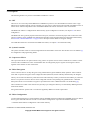
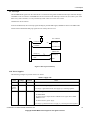
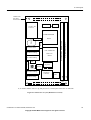
•
EJTAG Trace
Core board Connectors J3 / J4
CBUS
COP Interface
MIPS
CPU and SOC-it™
FPGA
PCI
MIPS
COP
FPGA
PC2100 SDRAM
Optional
Flash
PC100 SDRAM
Battery
EPROM
Mictor debug
USB
Controller
Clock
Generation
User Clocks
(From Header)
Power
Supply
Figure 1 Overview
NOTE: The CoreFPGA™ 3 board has the physical ability to mount a DDR SDRAM DIMM but support for this option
is not currently provided by the SOC-it™ system controller.
CoreFPGA™ 3 Users’ Manual, Revision 01.00
Copyright © 2005 MIPS Technologies Inc. All rights reserved.
5
1 Installation
1 Installation
Before use, the supplied (or other suitable) SDRAM SDR or DDR DIMM should be mounted in the socket provided.
For SDR DIMMs the modules must be capable of 2-cycle CAS latency so PC100-2-2-2 or any PC133 modules must be
used. For DDR PC2100 or better DIMMs are required.
The CoreFPGA™ 3 board is placed on the motherboard where an asymmetrically-placed mounting pillar on the
motherboard prevents reverse insertion.
The CoreFPGA™ 3 board comes with the CPU already programmed in the FPGA and ready to boot. If the optional
coprocessor is present, it is programmed in the coprocessor FPGA.
At boot time the YAMON monitor will output the type of CPU that is present on the board to the motherboard’s serial
port. The YAMON command "info cpu" will also show the CPU type, see Ref [1] on how to connect to he motherboard’s
serial port.
See Appendix A for USB download if new code for the CPU or the optional coprocessor must be downloaded to the
board.
If using a standard 14 pin EJTAG probe for debug, this must be connected to the appropriate EJTAG connector on the
motherboard, see Ref [1]. If using a Trace connector, this is attached to J11on the daughter card. Note that only one debug
probe can be connected at the time.
CoreFPGA™ 3 Users’ Manual, Revision 01.00
Copyright © 2005 MIPS Technologies Inc. All rights reserved.
6
2 Description
2 Description
The following features are present on the MIPS CoreFPGA™ 3 board.
2.1 CPU
The CPU is one of several possible MIPS32™ or MIPS64™ processor cores downloaded in a Xilinx Virtex-4 type
FPGA and is combined with the system controller [see next section]. The board can be mounted with different sizes of
Xilinx Virtex-4 FPGAs dependent on how the different MIPS CPUs fit into the Xilinx Virtex-4 architecture
The MIPS CPU FPGA is configured from Flash memory by the configuration controller, see chapter 2.5 for FPGA
configuration.
The MIPS CPU has 8 general purpose functional control pins, which are connected to jumper JP2 on the board. This
jumper is used for setting of MIPS CPU Initialisation Interface signals and miscellaneous configuration functionality,
see Section B, "Header Definitions" on page 28 for a description of the default "as shipped" settings.
Two LEDs D4 and D5 are connected to the MIPS CPU FPGA, see chapter 5 for LED functionality.
2.2 System Controller
The system controller is SOC-it™ and is integrated into the same FPGA as the CPU. See the SOC-it™ User Manual [3]
for configuration and programming details.
2.3 Coprocessor FPGA
The coprocessor FPGA is an option which is only present on specific versions of the CoreFPGA™ 3 board. For those
variants of the CoreFPGA™3 with a second FPGA there are 400 general purpose signals connecting the 2 FPGA
together with a number of clock connections.
2.4 FPGA Encryption
Virtex-4 devices have an on-chip decryptors using Advanced Encryption Standard (AES) operation. Xilinx software
tools offer an optional encryption of the configuration data (bitstream) with an AES key determined by the designer.
The keys are stored in the FPGA by JTAG instruction and retained by a battery connected to the VBATT pin, when the
device is not powered. Virtex-4 devices can be configured with the corresponding encrypted bitstream. A detailed
description of how to use bitstream encryption is provided in the Virtex-4 Platform FPGA User Guide Ref [[2]]
The CoreFPGA™ 3 board comes with the encrytion keys pre-configured. The keys are allocated by MIPS against the
board serial number.
Encrypted bit files for specific CPU’s can then be supplied by MIPS to customer requirement.
2.5 FPGA Configuration
A 16M x 8 bit Flash memory is used to hold the code for the MIPS CPU FPGA and the optional MIPS coprocessor FPGA
and a Cypress EZ-USB controller is used to control FPGA configuration. It provides two different functions:
• USB download of FPGA configuration code to Flash memory.
CoreFPGA™ 3 Users’ Manual, Revision 01.00
Copyright © 2005 MIPS Technologies Inc. All rights reserved.
7
2 Description
• Configuration of MIPS CPU FPGA and optional MIPS coprocessor FPGA from Flash memory.
When the board powers on the reset signal RSTN will remain asserted until the FPGAs are successfully configured, see
Chapter 2.6 for reset sequence.
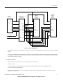
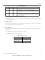
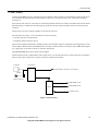
If a file download on the USB connector is detected, the configuration controller will enter the Flash programming mode,
where it receives the FPGA configuration image from the USB and programs it into the Flash memory. See Figure 2 for
USB download. When reception is complete it will assert PROGRAMN resulting in the new FPGA configuration code
being loaded into the FPGAs, and also resulting in the reset sequence being initiated, see Chapter 2.6 for reset sequence.
Config.
Controller
Data
Address
Control
Flash
Memory
USB
Figure 2 USB download
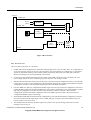
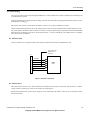
At power on or if new FPGA configuration code is downloaded the MIPS CPU FPGA and optional MIPS coprocessor
FPGA are configured by the configuration controller from Flash memory.
When the FPGAs have detected good power and are ready for configuration code download they assert the INITN signal
to the configuration controller. The configuration controller starts to load from the Flash memory to the FPGAs. The two
DONE signals from the FPGAs are pulled active when they are successfully configured, and this sets the
CONFIG_DONE signal to the reset circuitry. See Figure 3 for FPGA configuration.
CoreFPGA™ 3 Users’ Manual, Revision 01.00
Copyright © 2005 MIPS Technologies Inc. All rights reserved.
8
2 Description
Flash
Memory
D[7:0]
A[22:0]
MIPS
CPU
FPGA
Configuration
Controller
D[7:0]
A[22:0] DONE0
Optional
MIPS
COP
FPGA
D[7:0]
D[7:0]
DONE
DONE
DONE1
STS
STS
INITN
INITN
INITN
RDN
RDN
BUSY
BUSY
BUSY
WRN
WRN WRITEN
CSN
CSN
PROGN
CCLK
To LED D6
CSN0
To LED D1
CONFIG.
CSN1
DONE
and reset circuitry
WRITEN
WRITEN
PROGRAMN
PROGRAMN
CCLK
CCLK
CSN
CSN
Figure 3 FPGA configuration
The application code for the configuration controller is stored in an I2C EPROM, and the controller runs from a 12MHz
crystal.
The LED D6 indicates that the Flash memory is selected, which means either that FPGA configuration or USB download
is in progress. Should any of those fail, LED D6 flashes. The FPGA/FPASH state can be interpreted by looking at LEDs
D1 and D6, see Chapter 5 Table 6.
2.6 Reset sequence
There are three events that can cause the reset sequence to be activated:
• Power on reset
• USB reset sequence received, possibly in connection with download of new FPGA configuration code.
• Reset initiated from motherboard.
See Figure 4 for a description of the CoreFPGA™ 3 reset circuitry and the chapters below for a description of the
different reset sequences.
CoreFPGA™ 3 Users’ Manual, Revision 01.00
Copyright © 2005 MIPS Technologies Inc. All rights reserved.
9
2 Description
J3 & J4
CORE_OK
D1V2
D2V5
Voltage
Detector
CPWR_OK
CONFIG_DONE
Config.
Controller
&
DONE1
DONE0
USB
MIPS
CPU
FPGA
CP_RESET
MIPS
COP
FPGA
Optional
RSTN
Figure 4 Reset circuitry
2.6.1 Power on reset
The reset sequence at power on is as follows:
1.
CPWR_OK from the motherboard is deasserted, indicating that power is not yet stable. The 1.2V voltage detector
on the Core board is waiting for this rail to become stable. None of the FPGAs are configured yet, so the DONE
signals are deasserted resulting in the CONFIG_DONE signal being deasserted. The CORE_OK is therefore
deasserted resulting in the reset signal RSTN to be asserted.
2.
At some point, the motherboard supplies become stable, and CPWR_OK becomes active. Similarly, the Core
board voltage detector also start to indicate good power when the 2.5V voltage is stable.
3.
When the FPGAs themselves detect power ok they start to clear their internal configuration memory, and when this
is done they are ready to receive configuration code and therefore deassert the open drain signal INITN causing the
configuration controller to start download configuration code in the MIPS CPU FPGA.
4.
Once the MIPS CPU FPGA is configured the DONE0 signal is driven high causing the configuration controller to
read the DONE1 signal from the optional MIPS coprocessor FPGA. If that FPGA is not present DONE1 is pulled
high and the configuration controller continues to the next bullet. If however DONE1 is deasserted the
configuration controller downloads configuration code in the MIPS coprocessor FPGA. When this FPGA is
configured the DONE1 signal is driven high.
5.
With DONE0 and DONE1asserted the FPGA configuration process has finished and the configuration controller
drives the CONFIG_DONE signal high. This sets CORE_OK high, to signal to the motherboard that the Core
board is ready to come out of reset.
6.
The motherboard now deasserts the RSTN signal. The system is now up and running and the CPU can start
fetching its boot vector etc.
CoreFPGA™ 3 Users’ Manual, Revision 01.00
Copyright © 2005 MIPS Technologies Inc. All rights reserved.
10
2 Description
2.6.2 USB download
The USB download reset sequence is triggered if the configuration controller starts to receive FPGA configuration code
from the USB interface:
1.
When the configuration controller starts receiving data from the USB interface - more specifically the "!R"
sequence - it will deassert the CONFIG_DONE signal, causing the CORE_OK signal to be deasserted and thereby
resulting in the reset signal RSTN to be asserted.
2.
Configuration data received from USB is written into Flash memory.
3.
When receiving the sequence ">#DL_DONE" from USB, the configuration controller leaves its programming
state.
4.
At this point there are two possibilities:
• no flash data was received since last "!R", (i.e. the download file was empty) so the configuration controller
simply drives the CONFIG.DONE signal high, which results in CORE_OK going high to finish the reset
sequence.
• Flash memory data has been recieved between "!R" and ">#DL_DONE"( i.e. a new configuration has been
downloaded) so the configuration controller now deasserts PROGRAMN, thereby forcing the FPGAs to clear
their configuration memory.
5.
The rest of the sequence is identical to Chapter 2.6.1 bullet 3 to bullet 6.
2.6.3 Reset initiated from the motherboard
A reset initiated from the motherboard happens when the motherboard asserts RSTN and deasserts it again, see Ref [[1]].
This type of reset does not cause the FPGAs to be reconfigured since there is no change in the configuration code.
2.7 SDRAM
The MIPS CoreFPGA™ 3 board has sockets for either a conventional SDR SDRAM module (J2) or a DDR module (J1).
SDR modules must be capable of 2-cycle CAS latency at 100MHz. A PC100-222 or any PC133 module will satisfy this
condition. For DDR PC2100 or better modules should be used.
NOTE: As noted in the introduction the current version of SOC-it™ built into the FPGA(s) does not support DDR
SDRAM.
Parity signals are connected and can be used if desired.
The CPU can access the DIMM’s serial Serial Presence Detect EEPROM via the SOC-it™ system controller, in order
to identify the module characteristics. The Serial Presence Detect EEPROM is accessed on I2C slave address 0x50.
Note that if the installed module differs from the value set by the JP3 header Yamon will report an error and not boot.
2.8 CBUS
The CBUS is the motherboards simple bus interface, for access to the boot PROM and other devices where a more direct
access than that available through the PCI bus is required. The CBUS is connected via connector J3 to the main CPU/SC
FPGA. All accesses on the CBUS are 32 bit wide. See Ref. [[1]] for description of the CBUS protocol.
CoreFPGA™ 3 Users’ Manual, Revision 01.00
Copyright © 2005 MIPS Technologies Inc. All rights reserved.
11
2 Description
2.9 Interrupts
The INTERRUPTN signal from the CPU FPGA is connected to the global motherboard interrupt controller through
CINTHIN on the J3 connector. INTERRUPTN in fact comes from the Interrupt Control Unit (ICU) that is part of the
SOC-it™ system controller; it is only activated by either a PCI error or the ICU’s timer.
CINTLON is driven inactive.
From the motherboard, the 6 interrupt signals INTN[5:0] and the NMI signal, INMIN are taken to the MIPS CPU.
Note that the motherboard INN[5:4] signals are not used by the CPU core.
J3
SC in FPGA
CINTLON
NC
CINTHIN
PCI_INTN
INTERRUPTN
MIPS CPU
INTN[5:0]
6
NMI
INTN[5:0]
NMI
Figure 5 Interrupt connectivity
2.10 Power Supplies
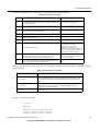
The following voltages are present on the Core board:
Table 1 Supply rails
Name
Voltage
VCORE
_FPGA
(D1V2)
1.2V
D2V5
2.5V
Current
8A
Notes
This is the core voltage supply to the FPGAs.
The voltage is generated from the 12V supply by a switching regulator.
1A
This is the supply for
• the DDR DIMM
• the Xilinx FPGA’s outputs that drive DRAM control signals when a DDR
DIMM is in use.
• the FPGA auxiliary power supply.
The voltage is generated from the 5V supply by a low drop-out linear regulator.
CoreFPGA™ 3 Users’ Manual, Revision 01.00
Copyright © 2005 MIPS Technologies Inc. All rights reserved.
12
2 Description
Table 1 Supply rails
Name
Voltage
Current
Notes
D3V3
3.3V
2A
This is the supply to all 3.3V devices on the board, including the 3.3V IO supply to the FPGAs. The voltage is supplied by the motherboard.
D5V
5V
4A
This is the supply to all 5V devices on the board including the switching power
supplies generating the D1V5 voltage. The voltage is supplied by the motherboard.
D12V
12V
0.5A
This is the supply to the 12V fan connector. It is also used for gate drive to the
external MOSFETs in the switching power supply circuit. The voltage is supplied by the motherboard.
Voltage measurement testpoints are available for all supply rails.
The VCORE_FPGA supply is derived from the 12V rail from the motherboard, using a switching regulator as the power
requirement is quite high.
2.11 Debug features
Four Mictor Logic Analyzer connectors J9, J10, J11and J12 are connected to the FPGA and carry the CPU’s system bus
signals for the purpose of diagnosing hard to find s/w faults.
2.12 Revision Register
The CoreFPGA™ 3 board has a hard-wired board and revision code which can be read from the REVISION register on
the motherboard.
The CORID field (6 bits) is always 0x09 for CoreFPGA™ 3 boards.
The CORRV field (2 bits) is given in the following table:
Table 2 CORRV Revision Field
CoreFPGA™ 3 revision
CORRV (2 bits)
01 (Dual FPGA)
0x0
01 (Single FPGA)
0x1
02 (Dual FPGA)
0x2
CoreFPGA™ 3 Users’ Manual, Revision 01.00
Copyright © 2005 MIPS Technologies Inc. All rights reserved.
13
3 Testpoints
3 Testpoints
The following testpoints are fitted.
Table 3 Testpoints
Silk screen
Function
CLK
Clock to FPGAs, SDRAM, and Mictor connectors J7, J8 and J9.
TP2
1.2V
D2V5
2.5V
D3V3
3.3V
D12V
12V
GND
GND (several of these)
FPGA1
Connected to FPGA output (use is reserved)
FPGA2
Connected to FPGA output (use is reserved)
CoreFPGA™ 3 Users’ Manual, Revision 01.00
Copyright © 2005 MIPS Technologies Inc. All rights reserved.
14
4 Connectors
4 Connectors
The following connectors are present on the board.
Table 4 Connectors
Label
Type
Function
J1
184 pin DIMM
Connector for PC2100 SDRAM Module.
J2
168 pin DIMM
Connector for PC100 SDRAM Module.
J3
200-way
Motherboard connector J3 as defined in Ref [[1]].
J4
200-way
Motherboard connector J4 as defined in Ref [1].
J5
38pin Mictor
J6
SMA
J7
USB type B
USB programming connector for download of FPGA configuration code to
Flash memory.
J9 - J12
38pin Mictor
Debug connectors for CPU System Interface signals.
J16
6 pin header
FPGA JTAG configuration connector for the MIPS CPU FPGA and
optional MIPS coprocessor FPGA. This is for MIPS internal use only.
J19
2 pin socket
Socket for FPGA encryption key retention battery.
Can only be replaced when the board is powered up.
J20
8pin 2mm header
EJTAG Trace debug connector.
External clock source. 50 ohm terminated.
Source of external FPGA clocks.
CoreFPGA™ 3 Users’ Manual, Revision 01.00
Copyright © 2005 MIPS Technologies Inc. All rights reserved.
15
5 LEDs
5 LEDs
The following LEDs are fitted to the board.
Table 5 LEDs
LED
Color
Function
Marking
D9
Green
All FPGA configuration done - see table below.
CONFIG
DONE
D8
Green
1.2V on Core board is ok.
(None)
D7
Green
Core board is ready.
(None)
D6
Yellow
MIPS CPU Status output 1 - Use is reserved
(None)
D5
Yellow
MIPS CPU Status output 2. - Use is reserved.
(None)
D4
Yellow
USB download status - see table below.
USB
The following table gives the meanings of the LED state when USB download / FPGA configuration is in progress. See
Appendix A.
Table 6 Flash download LEDs
D9 (green)
D4 (yellow)
Meaning
OFF
OFF
FPGA(s) are being configured by JTAG, and USB has no control
OFF
ON
1) The configuration controller is configuring FPGA(s) after power up or USB download.
2) USB download progress has stopped before the download is complete.
OFF
ON with very
short OFF blinks
Indication of progress in USB download.
OFF
Flashes
1) After power up: Bad flash content.
2) After USB download: Configuration controller has received garbage or bad flash content.
ON
OFF
Normal operation, FPGA(s) are configured and configuration controller is idle.
ON
ON
The configuration controller has entered Flash programming mode, with the FPGA(s) still
configured and running normal.
ON
Flashes
The configuration controller has received garbage in Flash programming mode, with the
FPGA(s) still configured and running normal.
CoreFPGA™ 3 Users’ Manual, Revision 01.00
Copyright © 2005 MIPS Technologies Inc. All rights reserved.
16
6 Jumpers
6 Jumpers
The following jumper headers can be fitted to the board.
Table 7 Board configuration jumpers
Jumper
Type
default
Function
JP1
2pin
notfit
Enables external clock from SMA connector J6. If fitted, the on board
clock oscillator in socket U6 must be removed.
JP2
16pin
2mm
header
notfit
2 pin
fit
Sets CPU Initialisation Interface and configuration signals.
See Section B, "Header Definitions"
Link must be in for SDR DIMM installed in J2.
JP3
Link must be out for DDR DIMM installed in J1
JP4
8 pin
2mm
header
Reserved for future use.
notfit
CoreFPGA™ 3 Users’ Manual, Revision 01.00
Copyright © 2005 MIPS Technologies Inc. All rights reserved.
17
7 Clock Circuitry
7 Clock Circuitry
Clocking of the MIPS processor, optional coprocessor and the system controller is controlled from a single clock source.
It can be either the onboard clock oscillator fitted in socket U6 or an external clock source connected to the SMA
connector J6.
If an external clock source is to be used it is connected to the SMA connector J6 which is terminated with 50 ohm. When
fitted the jumper J1 enables the external frequency generator, and the on board oscillator must be removed from the
socket U6.
Note that only 5V 8-pin oscillator modules can be used in socket U6.
The selected source drives, via a clock buffer circuit, the following:
• The CPU+System Controller FPGA.
• The Mictor debug connectors J9-J12.
The board as supplied is fitted with a 33MHz oscillator, the minimum frequency supported by the Digital DLLs in the
Virtex-4 FPGA. Downloads of some MIPS® CPU cores may run faster than this; if so please contact MIPS Technologies
Inc. support who wil be able to advise on oscillator replacement.
The DRAM DIMMs derive their clocks from the FPGA.
Note that the PCI clock is independent of this system clock. It is sourced from the J4 connector and only connected to
the PCI clock input on the SOC-it™ system controller contained in the FPGA.
Oscillator
Clock driver
SYSAD Mictor Connectors J7, J8 and J9
Jumper
SMA Connector
SDR DIMM clocks
FPGA
DDR DIMM clocks
External Clocks
Figure 6 Clock circuitry
CoreFPGA™ 3 Users’ Manual, Revision 01.00
Copyright © 2005 MIPS Technologies Inc. All rights reserved.
18
8 EJTAG debug
8 EJTAG debug
Two types of probes can be used to debug the MIPS CPU on the CoreFPGA™ 3 board, a standard 14 pin EJTAG probe,
or an EJTAG Trace probe.
If using a standard 14 pin EJTAG probe for debug, this must be connected to the appropriate EJTAG connector on the
motherboard, see Ref [[1]].
The EJTAG Trace probe is connected to the Mictor connector J11 on the CoreFPGA™ 3 board.
Note that the EJTCK signal from the 14 pin EJTAG probe connector on the motherboard is connected directly to the
TR_TCK signal on the EJTAG Trace connector in order to comply with the timing requirements in the EJTAG standard.
Therefore only one debug probe can be connected at the time, e.i. either a standard 14 pin EJTAG probe or an EJTAG
Trace probe can be connected.
8.1 EJTAG Chain
On the CoreFPGA™ 3 board the EJTAG chain from the motherboard contains the MIPS CPU only.
TR_TCK on J11
EJTAG Trace
connector
J3
EJDINT
EJTRSTN
EJTMS
EJTCK
MIPS
CPU
EJTDI
EJTDO
Figure 7 EJTAG connectivity
8.2 EJTAG Trace
The EJTAG Trace connector J11, allows all foreseen combinations of pinouts on the board. The connector is a Mictor
38-pin connector, allowing use of the 16-bit wide Trace output option.
Instead of an EJTAG Trace probe a Logic Analyzer can be connected to the Mictor connector J11 and used to monitor
the probe interface.
CoreFPGA™ 3 Users’ Manual, Revision 01.00
Copyright © 2005 MIPS Technologies Inc. All rights reserved.
19
9 PCB Layout
9 PCB Layout
This board complies to the standard size as described in Ref [[1]]. The placement of the major components is illustrated
in Figure 8. The 1V2 DC / DC converter, the FPGA configuration Flash and the EPLD shown in dotted line are situated
on the solder side of the PCB.
The sockets for the clock oscillator and configuration controller serial EEPROM are DIP 8 SMD sockets, i.e. only DIP
8 oscillators can be used.
Both Xilinx FPGAs are FF1513 Ball Grid Array packages which are 40mm x 40mm in with 39 x 39 pins full area
IMPORTANT NOTE: FPGA 1.2V Core Power Supply Fuse
As can be seen towards the top right hand corner of Figure 8 on page 21 there is a fuse present on the CoreFPGA™ 3
board. It is self-resetting and designed to limit the current into the FPGA to 8A. If the board suddenly stops working and
the green LED D8 goes out then the user should disconnect power from the Malta™ motherboard, wait 2 minutes, then
re-connect power and restart.
CoreFPGA™ 3 Users’ Manual, Revision 01.00
Copyright © 2005 MIPS Technologies Inc. All rights reserved.
20
9 PCB Layout
Offset from
the other
three holes
J3
JP2 CPU
JP4
1V2 DC / DC
Converter
J20
MIPS
CPU and SC
FPGA
J5 EJTAG Trace
J12 Mictor Debug
J11 Mictor Debug
2V5
OSC
J2 PC100 SDRAM Module
J1 PC2100 DDR SDRAM Module
Battery
Fuse
LEDs
Regulator
J6 Clock
PROM
Flash
JP1
J10 Mictor Debug
Download
Controller
USB
J9 Mictor Debug
J16 JTAG
J4
JP3
J3, J4: Samtec MOLC-150-31-x-Q, 200 pin (50 x 4) 1.27mm pitch connectors on underside.
Figure 8 CoreFPGA™ 3 Layout (Single FPGA version)
CoreFPGA™ 3 Users’ Manual, Revision 01.00
Copyright © 2005 MIPS Technologies Inc. All rights reserved.
21
9 PCB Layout
Offset from
the other
three holes
J3
JP2 CPU
JP4
1V2 DC / DC
Converter
COPROCESSOR
Fuse
J20
CPU CORE and
J12 Mictor Debug
SOC-it™
FPGA
J11 Mictor Debug
J2 PC100 SDRAM Module
J5 EJTAG Trace
J1 PC2100 DDR SDRAM Module
Battery
FPGA
OSC
LEDs
2V5
J6 Clock
Regulator
PROM
Flash
JP1
J10 Mictor Debug
Download
Controller
USB
J9 Mictor Debug
J16 JTAG
J4
JP3
J3, J4: Samtec MOLC-150-31-x-Q, 200 pin (50 x 4) 1.27mm pitch connectors on underside.
Figure 9 CoreFPGA™ 3 Layout (Dual FPGA version)
CoreFPGA™ 3 Users’ Manual, Revision 01.00
Copyright © 2005 MIPS Technologies Inc. All rights reserved.
22
9 PCB Layout
Appendices
CoreFPGA™ 3 Users’ Manual, Revision 01.00
Copyright © 2005 MIPS Technologies Inc. All rights reserved.
23
A USB download format
A USB download format
A USB connection to a host computer can be used to download new configuration bitfiles to the onboard Flash memory.
The CoreFPGA™ 3 board will present itself as a bidirectional printer device to the USB host. By using the printer class
the CoreFPGA™ 3 board can use existing printer drivers in e.g. Linux and Windows to access the board. In addition to
the control endpoint the board supports one bidirectional high-speed (12 Mbit/s) bulk endpoint:
Table 8 USB endpoints on CoreFPGA™ 3 board
Endpoint #
Direction (seen from host)
Type
0
IN
Control
0
OUT
Control
2
IN
Bulk
2
OUT
Bulk
Endpoint 0 is the standard control endpoint used to obtain e.g. device descriptors and stall/un-stall endpoints. Endpoint
0 supports all standard requests defined by the USB 1.1 standard as well as the additional requests defined for printer
class devices.
Endpoint 2 is a bidirectional bulk endpoint used for data transfer. The host will use the bulk-out pipe to send data to the
board. The use of the bulk-in pipe is optional as described below.
A.1 Sending data to the board
Data is send to the board through the bulk-out pipe. The exact method used to access the bulk-out pipe depends on the
operating system. For Linux the user can issue a command similar to:
cat xx.fl > /dev/usb/lp0
where xxxx.fl contains the data to send to the board and “/dev/usb/lp0” is the device interface for the bulk pipe.
For Windows the user must open the file in the Wordpad editor and “print” it to the port representing the CoreFPGA™
3 board. We suggest that all “.fl” files are associated with the Wordpad editor to assure that this editor is used to open the
files.
A.2 Reading data from the board
Since the board acts as a bi-directional printer it has a bulk-in pipe. The bulk-in pipe is used to retrieve information about
the CPU image stored in the on-board Flash, the revision of the configuration controller’s firmware and the configuration
state of the FPGA:
# Shows how to read info about the CPU Flash image,
# the configuration controller firmware revision and the FPGA state.
!r
>#GETINFO
#The board now waits for the user to read the information.
>#DL_DONE
Now issue a read from the USB pipe. The following command can be used on a Linux system (assuming the
CoreFPGA™ 3 is being downloaded through the Linux USB port /dev/usb/lp0, the device directory):
cat /dev/usb/lp0
CoreFPGA™ 3 Users’ Manual, Revision 01.00
Copyright © 2005 MIPS Technologies Inc. All rights reserved.
24
A USB download format
The saved information string is now shown on the screen together with the configuration controller’s firmware version.
Caution: The saved revision string is totally independent of the actual FPGA image in flash. To avoid a situation where
the information command reports a wrong FPGA code version, the MIPS flash file synthesis automatically appends
proper information to the flash image file, which may be inspected on a Linux system by
"tail xxxx.fl" where xxxx is the name of the flash download.
A.3 Remote reset via USB
It is possible to reset the whole Malta board via the USB port of the CoreFPGA™ 3 without reconfiguration of FPGAs.
For Linux the user can issue the command:
echo "!R>#DL_DONE" > /dev/usb/lp0
where “/dev/usb/lp0” is the device interface for the bulk pipe.
For Windows the user must edit the "!R>#DL_DONE" string in the Wordpad editor and “print” it to the port representing
the CoreFPGA™ 3 board
A.4 USB data format
The file sent to the board is a pure text file containing ASCII characters. The file contents is case insensitive (except for
’!r’/’!R’).
The boot Flash device is organized in sectors of 128 Kbyte. “Erase” and “Set Lock Bit” commands operate on exactly
one sector, this being the sector currently addressed. After the last block of 32 bytes in a sector are written into flash, the
address counter has advanced to the next sector. This implies that a Set Address (@) to the sector has to be executed
before a Set Lock Bit command (!S) can be issued.
The file to be loaded into the Flash via USB contains 3 types of elements: Commands, data and separators:
Table 9
Type
Description
Command
A command is build from an opcode and in some cases and argument, see next table.
Separator
Separators are used to separate commands and/or data. One or more of the following are
valid separators:
space, tab, LF or CR-LF.
Data
A 32 bit value like 11223344. Data must appear in blocks of 8 starting on a 8 word
boundary. The boot Flash itself is 8 bits wide and the 32 bits are stored in big endian
format so the value 11223344 is stored with 11 at the lowest address and 44 at the highest
address.
CoreFPGA™ 3 Users’ Manual, Revision 01.00
Copyright © 2005 MIPS Technologies Inc. All rights reserved.
25
A USB download format
A number of opcodes are used to control code download and Flash memory handling:
Table 10 Download commands
Opcode
Meaning
Argument
@
Sets current writing/erasing address (in CoreFPGA™ 3
Board physical memory map format). Addresses must be on
32-byte boundaries.
32 bit address, 8 characters.
!R
Reset board, select flash and enter download mode.
No
!r
Select flash and enter download mode.
Note that !r does not reset the board.
No
!E
Erase the current Flash sector (128 KB).
No
!C
Clear all Flash lock-bits.
No
!S
Set current Flash sector lock-bit.
No
#
Comment (rest of line).
A string of ASCII values between
0x20 and 0x7f except the ‘!r’ or ‘!R’
sequence. The controller
continuously looks for the ‘!’
character to get in sync if some error
occurs. So don’t use this sequence in
comments and display strings.
>
Display command (acts as comment on CoreFPGA™ 3 ).
Please note that display strings starting with # will be
interpreted as commands as well, see next table.
A string of exactly 8 ASCII values
between 0x20 and 0x7f except the
‘!r’ or ’!R’ sequence.
data
data has to be in blocks of 8 words, without interruption of
any Comments (#) and Print Commands (>).
No
Display commands where the string starts with # will be displayed but it will also be interpreted as commands according
to the table below.
Table 11 Special display commands
Display string
Meaning
#DL_DONE
This string brings the board out of USB download mode. Any characters
received after this display string will be skipped, until another ’!r’ or ’!R’
is received. This display string should be the last line in all download
files.
#GETINFO
This string will place the board in a mode where a text string stored in
flash can be retrieved by reading the USB port, together with the
configuration state of the FPGA.
#<others>
Reserved.
Example of code download format:
# Example
!R
@8fc00000
!E
12345678 23456789 3456789A 456789AB
56789ABC 6789ABCD 789ABCDE 89ABCDEF
9ABCDEF0 ABCDEF01 BCDEF012 CDEF0123
CoreFPGA™ 3 Users’ Manual, Revision 01.00
Copyright © 2005 MIPS Technologies Inc. All rights reserved.
26
A USB download format
DEF01234 EF012345 F0123456 01234567
# always 16 words in a block
>#DL_DONE
The example will reset the board, select the flash, erase the flash sector (size 128kbytes) starting at 8fc00.0000 and write
16 words starting at this address. Finally the board will return to normal operation due to the >#DL_DONE display
command.
If an error occurs the USB controller will ignore all data until the next !R/!r command. A !R/!r command will always
reset the download system regardless of state even if it occurs in the middle of a data stream.
The following commands will always bring the board out of download mode regardless of the previous state:
# Get in sync.
!r
# Back to normal operation
>#DL_DONE
The boot Flash device is 8 MBytes in size. These 8 MBytes are used as listed in the table below:
Table 12 Boot Flash layout
Area
Size
Usage
9f00.0000 ->
9f7f.ffff
8MBytes
Contains CPU FPGA configuration.
9f80.0000 ->
9fff.ffff
8 MBytes
Contains optional CoProcessor FPGA configuration.
CoreFPGA™ 3 Users’ Manual, Revision 01.00
Copyright © 2005 MIPS Technologies Inc. All rights reserved.
27
B Header Definitions
B Header Definitions
B.1 JP2
Pins
default
Function
1-2
Link Out
BE mode Link Out = Normal BE mode, Link In = Simple BE mode.
3-4
Link Out
Burst order for block reads Link Out = Wrap, Link In = SubBlock.
5-6
Link Out
SDRAM Data Width
Link Out = Full Width, Link In = Half Width.
7-8
Link Out
SOC-it:SDRAM clock ratio
Link Out = 1:1, Link In = 2:1.
CPU:SOC-it clock ratio
1:1: 13-14:11:12:9-10 = Out Out Out
2:1: 13-14:11:12:9-10 = Out Out In
3:1: 13-14:11:12:9-10 = Out In Out
9-10
11-12
13-14
Links Out
4:1: 13-14:11:12:9-10 = Out In In
3:2: 13-14:11:12:9-10 = In Out Out
5:2: 13-14:11:12:9-10 = In Out In
5:1: 13-14:11:12:9-10 = In In Out
7:2: 13-14:11:12:9-10 = In In In
15-16
Link Out
Reserved (MIPS internal use only)
Table 13 JP2 link definitions.
B.2 JP4
Reserved for future use.
B.3 J20 - External clock sources
This 8 pin header has a number of pins that allow external clock sources to be connected to the Virtex-4 FPGAs as either
inputs or outputs. As inputs they are connected to FPGA IOs defined as global clock inputs.
Pin 7: Ground
All other pins: Xilinx IO Standard = LVTTL.
CoreFPGA™ 3 Users’ Manual, Revision 01.00
Copyright © 2005 MIPS Technologies Inc. All rights reserved.
28
C References
C References
[1] MIPS Malta™ User’s Manual MD00048
[2] Xilinx Virtex-4 Platform FPGA User Guide.
[3] MIPS SOC-it™ System Controller User’s Manual. MD00163
CoreFPGA™ 3 Users’ Manual, Revision 01.00
Copyright © 2005 MIPS Technologies Inc. All rights reserved.
29
D Revision History
D Revision History
Revision
Date
Description
00.00
September 28, 2005
Initial version
00.01
September 29, 2005
Incorporated feedback & comments.
• Added Dual FPGA layout picture
01.00
September 30, 2005
• Added definitions for headers J20 and JP4.
• Swapped appendices B & C.
CoreFPGA™ 3 Users’ Manual, Revision 01.00
Copyright © 2005 MIPS Technologies Inc. All rights reserved.
30