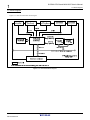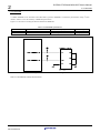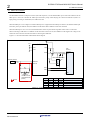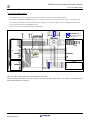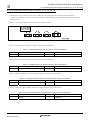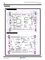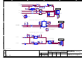
1
To our customers, Old Company Name in Catalogs and Other Documents On April 1st, 2010, NEC Electronics Corporation merged with Renesas Technology Corporation, and Renesas Electronics Corporation took over all the business of both companies. Therefore, although the old company name remains in this document, it is a valid Renesas Electronics document. We appreciate your understanding. Renesas Electronics website: http://www.renesas.com April 1st, 2010 Renesas Electronics Corporation Issued by: Renesas Electronics Corporation (http://www.renesas.com) Send any inquiries to http://www.renesas.com/inquiry. Notice 1. 2. 3. 4. 5. 6. 7. All information included in this document is current as of the date this document is issued. Such information, however, is subject to change without any prior notice. Before purchasing or using any Renesas Electronics products listed herein, please confirm the latest product information with a Renesas Electronics sales office. Also, please pay regular and careful attention to additional and different information to be disclosed by Renesas Electronics such as that disclosed through our website. Renesas Electronics does not assume any liability for infringement of patents, copyrights, or other intellectual property rights of third parties by or arising from the use of Renesas Electronics products or technical information described in this document. No license, express, implied or otherwise, is granted hereby under any patents, copyrights or other intellectual property rights of Renesas Electronics or others. You should not alter, modify, copy, or otherwise misappropriate any Renesas Electronics product, whether in whole or in part. Descriptions of circuits, software and other related information in this document are provided only to illustrate the operation of semiconductor products and application examples. You are fully responsible for the incorporation of these circuits, software, and information in the design of your equipment. Renesas Electronics assumes no responsibility for any losses incurred by you or third parties arising from the use of these circuits, software, or information. When exporting the products or technology described in this document, you should comply with the applicable export control laws and regulations and follow the procedures required by such laws and regulations. You should not use Renesas Electronics products or the technology described in this document for any purpose relating to military applications or use by the military, including but not limited to the development of weapons of mass destruction. Renesas Electronics products and technology may not be used for or incorporated into any products or systems whose manufacture, use, or sale is prohibited under any applicable domestic or foreign laws or regulations. Renesas Electronics has used reasonable care in preparing the information included in this document, but Renesas Electronics does not warrant that such information is error free. Renesas Electronics assumes no liability whatsoever for any damages incurred by you resulting from errors in or omissions from the information included herein. Renesas Electronics products are classified according to the following three quality grades: “Standard”, “High Quality”, and “Specific”. The recommended applications for each Renesas Electronics product depends on the product’s quality grade, as indicated below. You must check the quality grade of each Renesas Electronics product before using it in a particular application. You may not use any Renesas Electronics product for any application categorized as “Specific” without the prior written consent of Renesas Electronics. Further, you may not use any Renesas Electronics product for any application for which it is not intended without the prior written consent of Renesas Electronics. Renesas Electronics shall not be in any way liable for any damages or losses incurred by you or third parties arising from the use of any Renesas Electronics product for an application categorized as “Specific” or for which the product is not intended where you have failed to obtain the prior written consent of Renesas Electronics. The quality grade of each Renesas Electronics product is “Standard” unless otherwise expressly specified in a Renesas Electronics data sheets or data books, etc. “Standard”: 8. 9. 10. 11. 12. Computers; office equipment; communications equipment; test and measurement equipment; audio and visual equipment; home electronic appliances; machine tools; personal electronic equipment; and industrial robots. “High Quality”: Transportation equipment (automobiles, trains, ships, etc.); traffic control systems; anti-disaster systems; anticrime systems; safety equipment; and medical equipment not specifically designed for life support. “Specific”: Aircraft; aerospace equipment; submersible repeaters; nuclear reactor control systems; medical equipment or systems for life support (e.g. artificial life support devices or systems), surgical implantations, or healthcare intervention (e.g. excision, etc.), and any other applications or purposes that pose a direct threat to human life. You should use the Renesas Electronics products described in this document within the range specified by Renesas Electronics, especially with respect to the maximum rating, operating supply voltage range, movement power voltage range, heat radiation characteristics, installation and other product characteristics. Renesas Electronics shall have no liability for malfunctions or damages arising out of the use of Renesas Electronics products beyond such specified ranges. Although Renesas Electronics endeavors to improve the quality and reliability of its products, semiconductor products have specific characteristics such as the occurrence of failure at a certain rate and malfunctions under certain use conditions. Further, Renesas Electronics products are not subject to radiation resistance design. Please be sure to implement safety measures to guard them against the possibility of physical injury, and injury or damage caused by fire in the event of the failure of a Renesas Electronics product, such as safety design for hardware and software including but not limited to redundancy, fire control and malfunction prevention, appropriate treatment for aging degradation or any other appropriate measures. Because the evaluation of microcomputer software alone is very difficult, please evaluate the safety of the final products or system manufactured by you. Please contact a Renesas Electronics sales office for details as to environmental matters such as the environmental compatibility of each Renesas Electronics product. Please use Renesas Electronics products in compliance with all applicable laws and regulations that regulate the inclusion or use of controlled substances, including without limitation, the EU RoHS Directive. Renesas Electronics assumes no liability for damages or losses occurring as a result of your noncompliance with applicable laws and regulations. This document may not be reproduced or duplicated, in any form, in whole or in part, without prior written consent of Renesas Electronics. Please contact a Renesas Electronics sales office if you have any questions regarding the information contained in this document or Renesas Electronics products, or if you have any other inquiries. (Note 1) “Renesas Electronics” as used in this document means Renesas Electronics Corporation and also includes its majorityowned subsidiaries. (Note 2) “Renesas Electronics product(s)” means any product developed or manufactured by or for Renesas Electronics. User’s Manual SH7286 CPU board M3A-HS87 User’s Manual Renesas 32-Bit RISC Microcomputers SuperH™ RISC engine Family / SH7286 Group Rev.1.01 2009.06 Table of Contents Chapter 1 Overview ............................................................................................................................. 1-1 1.1 Introduction................................................................................................................................................................. 1-2 1.2 System Configuration ................................................................................................................................................. 1-2 1.3 Board Specifications................................................................................................................................................... 1-3 1.4 Exterior ....................................................................................................................................................................... 1-4 1.5 Block Diagram ............................................................................................................................................................ 1-5 1.6 Major Components ..................................................................................................................................................... 1-6 1.7 Memory Maps............................................................................................................................................................. 1-9 1.8 Absolute Maximum Ratings...................................................................................................................................... 1-11 1.9 Operating Conditions................................................................................................................................................ 1-11 Chapter 2 Functions ............................................................................................................................ 2-1 2.1 Overview of Functions ................................................................................................................................................ 2-2 2.2 CPU............................................................................................................................................................................ 2-3 2.3 Memory ...................................................................................................................................................................... 2-4 2.3.1 SH7286 On-chip memory.................................................................................................................................. 2-4 2.3.2 SDRAM ............................................................................................................................................................. 2-4 2.3.3 EEPROM........................................................................................................................................................... 2-6 2.4 Serial Port Interface.................................................................................................................................................... 2-7 2.5 I/O Ports ..................................................................................................................................................................... 2-8 2.6 Power Supply Module............................................................................................................................................... 2-11 2.7 USB Port Interface ................................................................................................................................................... 2-12 2.8 RCAN Port Interface................................................................................................................................................. 2-13 2.9 Clock Module............................................................................................................................................................ 2-14 2.10 Reset Module ......................................................................................................................................................... 2-15 2.11 Interrupt Switches................................................................................................................................................... 2-15 2.12 E10A-USB Interface ............................................................................................................................................... 2-16 Chapter 3 Operating Specifications ..................................................................................................... 3-1 3.1 Connectors ................................................................................................................................................................. 3-2 3.1.1 H-UDI Port Connectors (J1 and J2) .................................................................................................................. 3-4 3.1.2 Serial Port Connector (J3)................................................................................................................................. 3-6 3.1.3 Power Supply Connector (J4) ........................................................................................................................... 3-7 3.1.4 SH7286 External Power Supply Connectors (J5, J6, J17 and J18) .................................................................. 3-8 3.1.5 DC Power Supply Jack (J7) .............................................................................................................................. 3-9 3.1.6 Extension Connectors (J8 to J12, J16) ........................................................................................................... 3-10 3.1.7 RCAN Port Connector (J13)............................................................................................................................ 3-18 3.1.8 USB Port Connector (J14)............................................................................................................................... 3-19 3.1.9 GND connector (J15) ...................................................................................................................................... 3-20 3.2 Switches and LEDs .................................................................................................................................................. 3-21 3.2.1 CPU Power Switching Jumper (JP1)............................................................................................................... 3-22 3.2.2 External Power Switching Jumpers (JP2 to JP5) ............................................................................................ 3-23 3.2.3 RCAN Port Remove Jumpers (JP9 and JP10)................................................................................................ 3-24 Rev. 1.01 Jun. 09, 2009 REJ11J0028-0101 (i) 3.2.4 Switches and LEDs ......................................................................................................................................... 3-25 3.2.5 Jumper/Switch Setting when Using the Development Tools ........................................................................... 3-27 3.3 Dimensions............................................................................................................................................................... 3-28 Appendix.............................................................................................................................................A-1 M3A-HS87 SCHEMATICS Rev. 1.01 Jun. 09, 2009 REJ11J0028-0101 (ii) Chapter 1Overview Chapter 1 Overview 1-1 SH7286 CPU Board M3A-HS87 User's Manual 1 1.1 Introduction 1.1 Introduction The M3A-HS87 is a CPU board designed for users to evaluate the feature and performance of SH7286 group of Renesas Technology original microcomputer (MCU), as well as develop and evaluate the application software for the microcomputers described above. All the pins of SH7286 data bus, address bus and on-chip peripheral function are connected to the extension connector to allow user to evaluate the timing with peripheral devices using measurement instruments or develop extension boards according to the use. Furthermore, the on-chip E10A-USB emulator, (Renesas Technology) can be connected. 1.2 System Configuration Figure 1.2.1 shows an example of system configuration using M3A-HS87. 5V DC output * regulated power supply (1.5A min.) SH7286 CPU board M3A-HS87 Serial port connector USB port connector H-UDI port connector (14-pin or 36-pin) SH7286 RCAN port connector Extension connector E10A-USB emulator (1) High-performance Embedded Workshop (1) SuperH RISC engine C/C++ compiler package (1) USB Host computer (1) Note 1: These items are not included in this CPU board, and must be prepared by user. Figure 1.2.1 M3A-HS87 System Configuration Example Rev. 1.01 Jun. 09, 2009 REJ11J0028-0101 1-2 SH7286 CPU Board M3A-HS87 User's Manual 1 1.3 Board Specifications 1.3 Board Specifications Table 1.3.1 lists the M3A-HS87 board specifications. Table 1.3.1 Board Specifications No. Item Description SH7286 - Input (XIN) clock: 12.5 MHz - CPU clock: 100 MHz max. 1 CPU - Bus clock: 50 MHz max. - On-chip memory - Flash memory: 1024 KB - RAM: 32 KB - SDRAM: 16 MB (16-bit bus x 2), optional Notes: 2 External memory 1. SDRAM can be mounted only when SH7286 is used in 3.3 V 2. Bus width can be switched for 16-bit and 32-bit. -EEPROM: 128 kbit, optional HN58X24128FPIE: 1 (I2C bus connection) - Extension connectors (Bus, I/O, VCC, GND) - USB port connector (Series-B receptacle) 3 Connectors - Serial port connector (D-sub 9-pin) - RCAN port connector (D-sub 9-pin) - H-UDI port connector (14-pin) - H-UDI port connector (36-pin) 4 LEDs - Power supply LED: 1 - User LEDs: 6 - Reset switch : 1 - NMI switch :1 5 Switches - IRQ1 switch: 1 *1 - System setting DIP switches: 5/package - User DIP switches: 4/package - Dimensions: 100 mm x 160 mm 6 Board specification - Mounting form: 4 layers, double-sided - Number of board: 1 Note 1: Silk screen for this switch is printed as IRQ0. Rev. 1.01 Jun. 09, 2009 REJ11J0028-0101 1-3 1 SH7286 CPU Board M3A-HS87 User's Manual 1.4 Exterior 1.4 Exterior Figure 1.4.1 shows the M3A-HS87 exterior. Figure 1.4.1 M3A-HS87 Exterior Rev. 1.01 Jun. 09, 2009 REJ11J0028-0101 1-4 SH7286 CPU Board M3A-HS87 User's Manual 1 1.5 Block Diagram 1.5 Block Diagram Figure 1.5.1 shows the M3A-HS87 block diagram. Figure 1.5.1 M3A-HS87 Block Diagram Rev. 1.01 Jun. 09, 2009 REJ11J0028-0101 1-5 SH7286 CPU Board M3A-HS87 User's Manual 1 1.6 Major Components 1.6 Major Components Figure 1.6.1 and Figure 1.6.2 show the M3A-HS87 major components. JP3 External power switching jumper U5 RS-232C driver J11 Extension connector (optional) J12 Extension connector (optional) LED2 to LED7 User LEDs J7 DC power supply jack SW1 J4 Power supply LED1 Power switch Power supply LED supply connector JP1 CPU power switching jumper JP2 External power switching jumper J3 Serial port connector SDRAM (optional) U1 SH7286 J14 USB port connector J1 H-UDI port connector (36-pin) Bus, switch (optional) JP9, JP10 RCAN port remove jumpers J10 Extension connector (optional) J13 RCAN port connector J2 H-UDI port connector (14-pin) U11 RCAN driver J9 JP4, JP5 Extension SW3 External power connector User DIP J15 switching jumpers (optional) J8 switches GND J16 Extension Extension connector connector connector (optional) (optional) (optional) SW2 Reset switch J5, J17, J18, J6 SH7286 external power supply connectors (optional) U4 EEPROM (optional) SW5 NMI switch SW4 System setting DIP switches SW6 IRQ1 switch Figure 1.6.1 M3A-HS87 Major Components (Top View of the Component Side) Rev. 1.01 Jun. 09, 2009 REJ11J0028-0101 1-6 SH7286 CPU Board M3A-HS87 User's Manual 1 1.6 Major Components J11 Extension connector (optional) J7 DC power supply jack J12 Extension connector (optional) SDRAM (optional) J10 Extension connector (optional) Bus switch (optional) J16 Extension connector (optional) J8 Extension connector (optional) J9 Extension connector (optional) Figure 1.6.2 M3A-HS87 Major Components (Top View of the Solder Side) Rev. 1.01 Jun. 09, 2009 REJ11J0028-0101 1-7 SH7286 CPU Board M3A-HS87 User's Manual 1 1.6 Major Components Table 1.6.1 lists the major components on the M3A-HS87. Table 1.6.1 Major Components on the M3A-HS87 No. Name Part Number Manufacturer Name Remarks U1 CPU SH7286 Renesas U3, U4 Bus switches SN74CBTLV16211 TI Optional U5, U6 SDRAMs EDS1216AATA-75E ELPIDA Optional U16 EEPROM HN58X24128FPIE Renesas Optional U9 RS-232C driver SP3232ECA Sipex U11 RCAN transceiver HA13721RPJE Renesas U13 3.3 V regulator LM2738-YMY 550KHz N.S. U14 Reset IC M51957BFP Renesas X1 Oscillator SG8002DC_12.5MHz Epson Optional X1 Oscillator socket 110-83-308-41-001101 PRECI-DIP Optional X2 Crystal Units CX5032GB 12500 X3 Oscillator SG8002JF_48MHz Epson X4 Resonator (Ceralock) CSTCZ48M0X11R Murata X5 Resonator (Ceralock) CSTCE12M5G52R0 Murata J1 36-pin H-UDI port connector DX10M-36SE Hirose J2 14-pin H-UDI port connector 7614-6002BL 3M J3 Serial port connector XM2C-0942-132L OMRON J4 Power supply connector S2B-XH-A J.S.T. Mfg J5, J6, J17, SH7286 external power A2-2PA-2.54DSA Hirose J18 supply connectors J7 DC power supply jack HEC0470-01-630 HOSIDEN J8, J10, J11 20-pin extension connectors XG4C-2031 OMRON Optional J9,J12 40-pin extension connectors XG4C-4031 OMRON Optional J16 14-pin extension connector XG4C-1431 OMRON Optional KYOCERA KINSEKI J14 USB port connector UBB-4R-D14T-4D(LF)(SN) J.S.T. Mfg J13 RCAN port connector XM2C-0942-132L OMRON LED1 Power supply LED blue LED2 to 7 User LEDs green SW1 Power supply switch MS-12AAH1 Nikkai SW2 Reset switch B3SN-3012 OMRON SW3 User DIP switches A6S-4104 OMRON SW4 System setting DIP switches A6S-5104 OMRON SW5 NMI switch B3SN-3012 OMRON SW6 IRQ1 switch B3SN-3012 OMRON Rev. 1.01 Jun. 09, 2009 REJ11J0028-0101 Optional Optional Optional 1-8 SH7286 CPU Board M3A-HS87 User's Manual 1 1.7 Memory Maps 1.7 Memory Maps Figure 1.7.1 and Figure 1.7.2 show the memory map examples of SH7137 on the M3A-HS87. SH7286 logic space MCU mode 3 (Single-chip Mode) H'0000 0000 On-chip ROM (1024 KB) H'000F FFFF H'0010 0000 M3A-HS87 Memory Map H'0000 0000 H'000F FFFF H'0010 0000 Reserved Reserved H'801F FFFF H'8020 0000 H'802F FFFF H'8030 0000 On-chip flash memory Writing /Verifying space H'801F FFFF H'8020 0000 H'802F FFFF H'8030 0000 FFFF 0000 7FFF 8000 FFFF 0000 FFFF 0000 3FFF 4000 FFFF 0000 FFFF On-chip RAM (32 KB) Reserved SDRAM mode setting Trace RAM (16 KB) Reserved Peripheral I/O On-chip flash memory Writing /Verifying space Reserved Reserved H'FFF7 H'FFF8 H'FFF8 H'FFF8 H'FFFB H'FFFC H'FFFC H'FFFD H'FFFD H'FFFD H'FFFD H'FFFE H'FFFF On-chip ROM (1024 KB) H'FFF7 H'FFF8 H'FFF8 H'FFF8 H'FFFB H'FFFC H'FFFC H'FFFD H'FFFD H'FFFD H'FFFD H'FFFE H'FFFF FFFF 0000 7FFF 8000 FFFF 0000 FFFF 0000 3FFF 4000 FFFF 0000 FFFF On-chip RAM (32 KB) Reserved SDRAM mode setting Trace RAM (16 KB) Reserved Peripheral I/O Figure 1.7.1 SH7286 memory mapping example (MCU mode 3) Rev. 1.01 Jun. 09, 2009 REJ11J0028-0101 1-9 SH7286 CPU Board M3A-HS87 User's Manual 1 1.7 Memory Maps SH7286 logic space MCU mode 2 M3A-HS87 Memory Map (On-chip ROM enabled mode) H'0000 H'000F H'0010 H'01FF H'0200 H'03FF H'0400 0000 FFFF 0000 FFFF 0000 FFFF 0000 H'07FF FFFF H'0800 0000 H'0BFF H'0C00 H'0FFF H'1000 H'13FF H'1400 H'17FF H'1800 H'1BFF H'1C00 H'1FFF H'2000 FFFF 0000 FFFF 0000 FFFF 0000 FFFF 0000 FFFF 0000 FFFF 0000 On-chip ROM (1024 KB) Reserved CS0 space CS1 space CS2 space CS3 space CS4 space CS5 space CS6 space CS7 space H'0000 H'000F H'0010 H'01FF H'0200 H'03FF H'0400 H'07FF H'0800 H'0BFF H'0C00 H'0FFF H'1000 H'13FF H'1400 H'17FF H'1800 H'1BFF H'1C00 H'1FFF H'2000 0000 FFFF 0000 FFFF 0000 FFFF 0000 FFFF 0000 FFFF 0000 FFFF 0000 FFFF 0000 FFFF 0000 FFFF 0000 FFFF 0000 Reserved H'801F FFFF H'8020 F000 H'802F FFFF H'8030 0000 On-chip flash memory writing/verifying space FFFF 0000 7FFF 8000 FFFF 0000 FFFF 0000 3FFF 4000 FFFF 0000 FFFF On-chip RAM (32 KB) Reserved SDRAM mode setting Trace RAM (16 KB) Reserved Peripheral I/O Reserved User area User area User area SDRAM (16 MB) * User area User area User area User area User area Reserved H'801F FFFF H'8020 F000 H'802F FFFF H'8030 0000 On-chip flash memory writing/verifying space Reserved Reserved H'FFF7 H'FFF8 H'FFF8 H'FFF8 H'FFFB H'FFFC H'FFFC H'FFFD H'FFFD H'FFFD H'FFFD H'FFFE H'FFFF On-chip ROM (1024 KB) H'FFF7 H'FFF8 H'FFF8 H'FFF8 H'FFFB H'FFFC H'FFFC H'FFFD H'FFFD H'FFFD H'FFFD H'FFFE FFFF 0000 7FFF 8000 FFFF 0000 FFFF 0000 3FFF 4000 FFFF 0000 On-chip RAM (32 KB) Reserved SDRAM mode setting Trace RAM (16 KB) Reserved Peripheral I/O H'FFFF FFFF * SDRAM is optional. Figure 1.7.2 SH7286 memory mapping example (MCU mode 2) Rev. 1.01 Jun. 09, 2009 REJ11J0028-0101 1-10 SH7286 CPU Board M3A-HS87 User's Manual 1 1.8 Absolute Maximum Ratings 1.8 Absolute Maximum Ratings Table 1.8.1 lists the absolute maximum ratings of the M3A-HS87. Table 1.8.1 M3A-HS87 Absolute Maximum Ratings Symbol 5VCC Item Value Remarks 5 V system power supply voltage - 0.3 to 6.0 V VSS Topr Operating temperature 0°C to 50°C Do not expose to condensation or corrosive gas Tstr Storage temperature -10°C to 60°C Do not expose to condensation or corrosive gas Temperature refers to the air temperature in the vicinity of the board. 1.9 Operating Conditions Table 1.9.1 lists the operating conditions of the M3A-HS87. Table 1.9.1 M3A-HS87 Operating Conditions Symbol 5VCC Topr Item 5 V system power supply voltage Value 4.75 to 5.25 V Maximum current consumption 1.5 A max. Operating temperature 0°C to 50°C Rev. 1.01 Jun. 09, 2009 REJ11J0028-0101 Remarks Reference voltage: VSS Do not expose to condensation or corrosive gas 1-11 1 SH7286 CPU Board M3A-HS87 User's Manual 1.9 Operating Conditions This page intentionally left blank. Rev. 1.01 Jun. 09, 2009 REJ11J0028-0101 1-12 Chapter 2Functions Chapter 2 Functions 2-1 2 SH7286 CPU Board M3A-HS87 User's Manual 2.1 Overview of Functions 2.1 Overview of Functions The M3A-HS87 is the SH7286 CPU board that has functional modules listed in Table 2.1.1. Table 2.1.1 M3A-HS87 Functional Modules Sections 2.2 Features CPU Description SH7286 - Input (XIN) clock: 12.5 MHz - CPU clock: 100 MHz max. - Bus clock: 50 MHz max. - On-chip memory - Flash memory: 1024 KB - RAM: 32 KB 2.3 Memory - SDRAM: 16 MB (16 bit bus width x 2), optional * SDRAM can be used only when SH7286 is used at 3.3 V. * Bus width can be switched for 16-bit and 32-bit. - EEPROM: 128 kbit (optional) HN58X24128FPIE :1 (I2C bus connection) 2.4 Serial Port Interface Connects the SH7286 SCI0 pin to the serial port connector 2.5 I/O Ports Connect to the SH7286 I/O ports 2.6 Power Supply Module Controls the M3A-HS87 system power supply 2.7 USB Port Interface Connects the SH7286 USB pin to the USB port connector 2.8 RCAN Port Interface Connects the SH7286 RCAN pin to RCAN port connector via RCAN transceiver 2.9 Clock Module Controls the system clock 2.10 Reset Module Resets the devices mounted on the M3A-HS87 2.11 Interrupt Switches Connects to NMI pin and IRQ1 pin 2.12 E10A-USB Interface SH7286 H-UDI/AUD Interface Operating specifications Connectors, switches, LEDs - - SH7286 extension connectors - Switches, LEDs - H-UDI port connectors Refer to Chapter 3 for details. Rev. 1.01 Jun. 09, 2009 REJ11J0028-0101 2-2 2 SH7286 CPU Board M3A-HS87 User's Manual 2.2 CPU 2.2 CPU The M3A-HS87 includes SH7286, the 32-bit RISC microcomputer operates with a maximum frequency of 100 MHz. SH7286 is the microcomputer that has a 1024 KB flash memory and 32 KB on-chip RAM to support various application such as data processing and device control. SH7286 can be operated at 100 MHz of CPU clock frequency (50 MHz at maximum of external bus) when the input clock on the M3A-HS87 is at 12.5 MHz. Figure 2.2.1 shows the SH7286 block diagram on the M3A-HS87. SH7286 Clock EXTAL XTAL PA15/CK System control RES NMI WDTOVF User LEDs PE9/TIOC3B/FRAME PE11/TIOC 3D PE12/TIOC 4A PE13/TIOC 4B/MRES PE14/DACK0/TIOC4C/AH PE15/DACK1/TIOC4D/IRQOUT User DIP switches PE0/TIOC0A/TIOC 4AS/DREQ0 PE1/TIOC0B/TIOC 4BS/TEND0 PE2/TIOC0C/TIOC 4CS/DREQ1 PE3/TIOC0D/TIOC 4DS/TEND1 EEPROM USB Serial port Extension connector (J13) GPIO, Control signal, MTU2/2S, interrupt , etc RCAN port H-UDI System setting DIP switches PB2/SCL/POE1/IRQ0 PB3/SDA/POE2/IRQ1 USBXTAL USBEXTAL PB9/USPND VBUS USD+ USDPB10 PC0/A0/POE0 PC1/A1 PC2/A2 PC3/A3 PC4/A4 PC5/A5 PC6/A6 PC7/A7 PC8/A8 PC9/A9 PC10/A10 PC11/A11 PC12/A12 PC13/A13/IRQ0 PC14/A14/IRQ1 PC15/A15/IRQ2 PB0/A16/IRQ3 PB1/A17/REFOUT/ADTRG/IRQ4 PB6/A18/BACK/POE3/IRQ5/RXD0 PB7/A19/BREQ/POE4/IRQ6/TXD0 PB8/A20/WAIT/POE8/IRQ7/SCK0 PB15/CKE/A21 PB16/CASL/A22/DACK3 PB17/CASU/A23/DREQ3 PB18/RASL/A24/DACK2 PB19/RASU/A25/DREQ2 PD0/D0 PD1/D1 PD2/D2/TIC5U PA0/RXD0/CS0 PD3/D3/TIC5V PA1/TXD0/CS1 PD4/D4/TIC 5W PA2/SCK0/SCS/CS2 PD5/D5/TIC5US PA3/RXD1/SSI/CS3 PD6/D6/TIC5VS PA4/TXD1/SSO/CS4 PD7/D7/TIC 5WS PA5/SCK1/SSCK/CS5 PD8/D8/TIOC 3AS PA6/TCLKA/RASL PD9/D9/TIOC3CS PD10/D10/TIOC 3BS PA7/TCLKB/SCK3/CASL PA8/TCLKC/TXD3/RDWR PD11/D11/TIOC3DS PD12/D12/TIOC 4AS PA9/TCLKD/RXD3/CKE PA10/WRHL/DQMUL PD13/D13/TIOC 4BS PA11/WRHH/DQMUU/AH PD14/D14/TIOC4CS PD15/D15/TIOC4DS PA12/WRH/DQMLU/POE8 PD16/D16/IRQ0/CS3/AUDATA0 PA13/WRL/DQMLL PD17/D17/IRQ1/POE5/SCK3/CS2/AUDATA1 PA14/RD PA21/TIC5U/RASU/POE8/IRQ3/RASL PD18/D18/IRQ2/POE6/TXD3/CS1/AUDATA2 PA22/TIC5V/CASU/POE4/IRQ2/CASL PD19/D19/IRQ3/POE7/RXD3/CS0/AUDATA3 PA23/TIC5W/POE0/IRQ1/AH/CKE PD20/D20/IRQ4/TIC5WS/SCK4/POE8 PD21/D21/IRQ5/TIC 5VS/TXD4 PB11/RXD2/CS6/CS2/CS0/IRQ0/CS2 PD22/D22/IRQ6/TIC 5US/RXD4/AUDSYNC PB12/TXD2/CS7/CS3/CS1/IRQ1/CS3 PD23/D23 PB13/CTx0 PD24/D24/DREQ0/TIOC 4DS/AUDCK PB14/CRx0 PD25/D25/TIOC 4CS/DREQ1 PE4/TIOC 1A/RXD3 PD26/D26/TIOC 3BS/DACK1 PE5/TIOC 1B/TIOC 3BS/TXD3 PD27/D27/TIOC 4AS/DACK0 PE6/TIOC 2A/TIOC 3DS/SCK3 PD28/D28/TIOC 3DS PE7/TIOC 2B/RXD2/BS/UBCTRG PD29/D29/TIOC3BS PE8/TIOC 3A/SCK2 PD30/D30/TIOC 3CS/IRQOUT PE10/TIOC 3C/TXD2 PD31/D31/TIOC 3AS/ADTRG TDI TDO TCK TMS TRST ASEMD0 FWE/ASEBRKAK/ASEBRK MD1 MD0 Address bus Data bus AUD PF0/AN0 PF1/AN1 PF2/AN2 PF3/AN3 PF4/AN4 PF5/AN5 PF6/AN6 PF7/AN7 PF8/AN8 PF9/AN9 PF10/AN10 PF11/AN11 A/D DA0 DA1 D/A Figure 2.2.1 SH7286 Block Diagram Rev. 1.01 Jun. 09, 2009 REJ11J0028-0101 2-3 2 SH7286 CPU Board M3A-HS87 User's Manual 2.3.2 SDRAM 2.3 Memory 2.3.1 SH7286 On-chip memory The SH7286 MCU includes a 1024 KB flash memory and a 32 KB RAM. 2.3.2 SDRAM Two of 16 MB SDRAMs can be mounted on the M3A-HS87 (optional). As 3.3 V power is supplied to SDRAM on the M3A-HS87, use the SH7286 MCU at 3.3 V when using SDRAM. (Set the CPU power switching jumper JP1 as "2-3".) SDRAM is controlled by the SH7286 on-chip bus state controller. Specify the bus width to 16-bit when accessing one SDRAM. To access two SDRAMs, specify the bus width to 32-bit. When mounting SDRAM, mount two bus switches (PI3C16211A), a peripheral logic (HD74LV2G14A), resistors and capacitors. Also remove 0 Ω resistors, R44 to R49. Example A: To mount two SDRAMs of 16MB (for 8, 16 and 32-bit access) - Mount R5, R16 to R43, RA9 to RA14, CP22 to CP39, L4, and U2 to U6 - Remove R44 to R49 Example B: To mount one SDRAM of 16MB (for 8 and 16-bit access) - Mount R5, R16 to R21, R26 to R33, R38 to R43, RA11 to RA14, CP30 to CP39, L4, U2, U4 and U6 - Remove R44 to R49 Table 2.3.1 shows the summary of SDRAM specifications. Figure 2.3.1 shows the circuit diagram between SH7286 and SDRAM. Table 2.3.1 SDRAM specifications Item Description Configuration 2 M words x 16 bits x 4 banks: 2 Capacity 32 MB (8 M words/32 bits) Access time 5.4 ns CAS Latency 2 (at 50 MHz bus clock) Refresh interval 4096 cycles every 64 ms Row address A11 to A0 Column address A8 to A0 Number of banks 4 (controlled by BA0 and BA1) Rev. 1.01 Jun. 09, 2009 REJ11J0028-0101 2-4 2 SH7286 CPU Board M3A-HS87 User's Manual AUDATA0-3 AUDSYNC AUDCK D16-19,22,24 2.3.2 SDRAM Figure 2.3.1 SH7286-SDRAM Circuit Diagram Rev. 1.01 Jun. 09, 2009 REJ11J0028-0101 2-5 2 SH7286 CPU Board M3A-HS87 User's Manual 2.3.3 EEPROM 2.3.3 EEPROM A 128kbit EEPROM can be mounted on the M3A-HS87 (optional). EEPROM is controlled by the SH7286 on-chip I2C-bus interface. Table 2.3.2 lists the summary of EEPROM specifications. Figure 2.3.2 shows the circuit diagram between SH7286 and EEPROM. Table 2.3.2 EEPROM specifications Part number Interface Capacity Package HN58X24128FPIE I2C-bus interface (note) 128 kbit (16k words x 8 bits) 8-pin, SOP Figure 2.3.2 SH7211-EEPROM Circuit Diagram Note: I2C is the trademark of Philips semiconductors. Rev. 1.01 Jun. 09, 2009 REJ11J0028-0101 2-6 2 SH7286 CPU Board M3A-HS87 User's Manual 2.4 Serial Port Interface 2.4 Serial Port Interface On the M3A-HS87, SH7286 SCI channel 0 is connected to the serial port connector. Also, SH7286 SCI channel 0 is connected to the extension connector (J12). When using SH7286 SCI channel 0 as a serial port, do not connect it to the extension connector. Figure 2.4.1 shows the serial port block diagram on the M3A-HS87. RS-232C driver SH7286 0Ω NC PA0/RXD0/CS0 1 2 3 4 0Ω GND PA1/TXD0/CS1 5 6 7 8 NC 9 Serial port connector DCD RxD TxD DTR GND DSR RTS CTS RI Extension connector PA0/RXD0/CS0# PA1/TXD0/CS1# Figure 2.4.1 Serial Port Block Diagram Rev. 1.01 Jun. 09, 2009 REJ11J0028-0101 2-7 2 SH7286 CPU Board M3A-HS87 User's Manual 2.5 I/O Ports 2.5 I/O Ports SH7286 I/O ports are connected to the extension connector on the M3A-HS87. Some I/O ports are also connected to DIP switches and LEDs, and can be used at the user’s discretion. Figure 2.5.1 shows the connection diagram of LEDs and DIP switches. Table 2.5.1 lists functions of the I/O ports. LEDPWR H19 H20 H18 H17 H15 H16 LED2 green LED7 green LED6 green LED5 green LED4 green SH7286 PE9/TIOC3B/FRAME LED3 green PE11/TIOC3D PE12/TIOC4A PE13/TIOC4B/MRES PE14/DACK0/TIOC4C/AH PE15/DACK1/TIOC4D/IRQOUT VCC User DIP switches (SW3) SW3-1 0Ω SW3-2 0Ω SW3-3 0Ω SW3-4 0Ω PE0/TIOC0A/TIOC4AS/DREQ0 PE1/TIOC0B/TIOC4BS/TEND0 PE2/TIOC0C/TIOC4CS/DREQ1 PE3/TIOC0D/TIOC4DS/TEND1 Figure 2.5.1 Connection Diagram of LEDs and DIP Switches Rev. 1.01 Jun. 09, 2009 REJ11J0028-0101 2-8 2 SH7286 CPU Board M3A-HS87 User's Manual 2.5 I/O Ports Table 2.5.1 I/O Ports Functions No 1 2 6 7 8 9 10 11 12 13 14 15 16 17 18 19 20 21 24 25 26 27 28 29 30 31 32 33 36 37 38 39 40 41 42 43 46 47 48 49 50 51 52 53 57 58 59 60 61 62 63 64 65 68 69 70 71 72 73 74 SH7286 Pin Name PE14/DACK0/TIOC4C/AH PE15/DACK1/TIOC4D/IRQOUT PA23/TIC5W/POE0/IRQ1/AH/CKE PA22/TIC5V/CASU/POE4/IRQ2/CASL PA21/TIC5U/RASU/POE8/IRQ3/RASL PC0/A0/POE0 PC1/A1 PC2/A2 PC3/A3 PC4/A4 PC5/A5 PC6/A6 PC7/A7 PC8/A8 PC9/A9 PC10/A10 PC11/A11 PC12/A12 PC13/A13/IRQ0 PC14/A14/IRQ1 PC15/A15/IRQ2 PB0/A16/IRQ3 PB1/A17/REFOUT/ADTRG/IRQ4 PB2/SCL/POE1/IRQ0 PB3/SDA/POE2/IRQ1 PB6/A18/BACK/POE3/IRQ5/RXD0 PB7/A19/BREQ/POE4/IRQ6/TXD0 PB8/A20/WAIT/POE8/IRQ7/SCK0 PD0/D0 PD1/D1 PD2/D2/TIC5U PD3/D3/TIC5V PD4/D4/TIC5W PD5/D5/TIC5US PD6/D6/TIC5VS PD7/D7/TIC5WS PD8/D8/TIOC3AS PD9/D9/TIOC3CS PD10/D10/TIOC3BS PD11/D11/TIOC3DS PD12/D12/TIOC4AS PD13/D13/TIOC4BS PD14/D14/TIOC4CS PD15/D15/TIOC4DS PD16/D16/IRQ0/CS3/AUDATA0 PD17/D17/IRQ1/POE5/SCK3/CS2/AUDATA1 PD18/D18/IRQ2/POE6/TXD3/CS1/AUDATA2 PD19/D19/IRQ3/POE7/RXD3/CS0/AUDATA3 PD20/D20/IRQ4/TIC5WS/SCK4/POE8 PD21/D21/IRQ5/TIC5VS/TXD4 PD22/D22/IRQ6/TIC5US/RXD4/AUDSYNC PD23/D22 PD24/D24/DREQ0/TIOC4DS/AUDCK PD25/D25/TIOC4CS/DREQ1 PD26/D26/TIOC4BS/DACK1 PD27/D27/TIOC4AS/DACK0 PD28/D28/TIOC3DS PD29/D29/TIOC3BS PD30/D30/TIOC3CS/IRQOUT PD31/D31/TIOC3AS/ADTRG J8 J9 Extension Connectors J10 J11 J12 9 9 9 9 9 Remarks J16 LED LED IRQ1 switch 9 9 9 9 9 9 9 9 9 9 9 9 9 9 9 9 9 9 EEPROM EEPROM 9 9 9 9 9 9 9 9 9 9 9 9 9 9 9 9 9 9 9 9 9 9 9 9 9 9 9 9 9 9 9 9 9 9 9 9 9 9 9 9 9 9 9 Legend: 9: The pin can be connected to the extension connector specified at the top of this table. : The pin can only be connected to the extension connector specified at the top of this table when a 0 Ω resistor is mounted. Rev. 1.01 Jun. 09, 2009 REJ11J0028-0101 2-9 2 SH7286 CPU Board M3A-HS87 User's Manual 2.5 I/O Ports Table 2.5.2 I/O Ports Functions No 77 78 79 80 81 82 83 84 85 86 96 97 98 99 100 105 111 120 121 122 123 124 125 126 129 130 131 132 133 138 139 140 141 142 143 144 145 150 151 152 153 158 159 162 163 164 165 166 167 168 169 171 172 173 174 175 176 SH7286 Pin Name PA15/CK PA14/RD PA13/WRL/DQMLL PA12/WRH/DQMLU/POE8 PA11/WRHH/DQMUU/AH PA10/WRHL/DQMUL PA9/TCLKD/RXD3/CKE PA8/TCLKC/TXD3/RDWR PA7/TCLKB/SCK3/CASL PA6/TCLKA/RASL PB15/CKE/A21 PB16/CASL/A22/DACK3 PB17/CASU/A23/DREQ3 PB18/RASL/A24/DACK2 PB19/RASU/A25/DREQ2 PB9/USPND PB10 PE0/TIOC0A/TIOC4AS/DREQ0 PE1/TIOC0B/TIOC4BS/TEND0 PE2/TIOC0C/TIOC4CS/DREQ1 PE3/TIOC0D/TIOC4DS/TEND1 PE4/TIOC1A/RXD3 PE5/TIOC1B/TIOC3BS/TXD3 PE6/TIOC2A/TIOC3DS/SCK3 PB11/RXD2/CS6/CS2/CS0/IRQ0/CS2 PB12/TXD2/CS7/CS3/CS1/IRQ1/CS3 PB13/CTx0 PB14/CRx0 RESET PF0/AN0 PF1/AN1 PF2/AN2 PF3/AN3 PF4/AN4 PF5/AN5 PF6/AN6 PF7/AN7 PF8/AN8 PF9/AN9 PF10/AN10 PF11/AN11 DA0 DA1 WDTOVF PA0/RXD0/CS0 PA1/TXD0/CS1 PA2/SCK0/SCS/CS2 PA3/RXD1/SSI/CS3 PA4/TXD1/SSO/CS4 PA5/SCK1/SSCK/CS5 PE7/TIOC2B/RXD2/BS/UBCTRG PE8/TIOC3A/SCK2 PE10/TIOC3C/TXD2 PE9/TIOC3B/FRAME PE11/TIOC3D PE12/TIOC4A PE13/TIOC4B/MRES J8 J9 9 Extension Connectors J10 J11 J12 9 Remarks J16 9 9 9 9 9 9 9 9 9 9 9 9 9 9 9 9 9 User DIP switches User DIP switches User DIP switches User DIP switches 9 9 9 9 9 9 9 9 9 9 9 9 9 9 RCAN output pin RCAN input pin RESET Analog input pin Analog input pin Analog input pin Analog input pin Analog input pin Analog input pin Analog input pin Analog input pin Analog input pin Analog input pin Analog input pin Analog input pin Analog input pin Analog input pin 9 J3 J3 9 9 9 9 9 9 9 LED LED LED LED 9 9 9 9 Legend: 9: The pin can be connected to the extension connector specified at the top of this table. : The pin can only be connected to the extension connector specified at the top of this table when a 0 Ω resistor is mounted. Rev. 1.01 Jun. 09, 2009 REJ11J0028-0101 2-10 2 SH7286 CPU Board M3A-HS87 User's Manual 2.6 Power Supply Module 2.6 Power Supply Module A 5 V DC is input to the M3A-HS87, and the generator on the M3A-HS87 generates 3.3 V DC. As it is a step down DC-DC switching regulator, the desired voltage can be generated by changing resistance value. 5 V DC power supply can be supplied from both DC regulated power supply (via J4 power connector) and AC adaptor (via J7 DC power supply jack) System power of SH7286 (VCC) can be switched back and forth between 3.3 V and 5 V by power switching jumper (JP1). The default setting is at 5 V. When switching the VCC, follow the notes described below. Note: When mounting SDRAM with 5 V DC setting, voltages beyond the maximum ratings may be supplied from the address bus, data bus and control bus and it may cause malfunction in device. Pay close attention for the setting. The SH7286 system power (VCC), A/D power supply (AVCC), AVREF power supply and USB power supply (DrVCC) can be supplied from external power supply separately using the jumper settings. Figure 2.6.1 shows the M3A-HS87 power supply circuit diagram. Extension connector AVCC External power supply J8 connector SH7286 5VCC AVCC JP4 External power AVREF supply J8 connector 5VCC J4 Power supply connector 5 V DC input AVREF Power supply switch JP5 External power supply 3.3 V/5 V Power switching jumper (JP1) 5VCC 1 J7 DC power supply jack 3 JP VCC 2 JP2 VCC_CPU External power supply 5VCC 5V 3.3 V DrVCC (USB power supply) 3VCC JP3 SDRAM Extension connector This is optional, and can be mounted when using the SH7286 at 3.3 V. Figure 2.6.1 Power supply Block Diagram Rev. 1.01 Jun. 09, 2009 REJ11J0028-0101 2-11 2 SH7286 CPU Board M3A-HS87 User's Manual 2.7 USB Port Interface 2.7 USB Port Interface The M3A-HS87 includes a USB port connector (Series-B receptacle). Use the SH7286 PB10 pin to control the USB line. Set the PB10 pin to a low level to disable the VBUS input and USD+ pull-up when delaying the connection notification (such as in high-priority processing or initialization) to a USB host or hub. When the PB10 pin is set to a high level and the VBUS power is supplied from the USB port connector, the SH7286 VBUS input and USD+ pull-up are enabled. Then, the USB host or hub detects that a USB device has been connected. When the VBUS pin is set to a low level, the SH7286 MCU retains its powered state regardless of the USD+ or USD- state. When connecting a USB cable to a USB host or hub when this board is not ON, the USB host or hub supplies the voltage to the VBUS. Be sure to turn the CPU board ON before connecting the USB cable. Figure 2.7.1 shows the M3A-HS87 USB interface block diagram. VCC_CPU (3.3 V/5 V) 3.3 V SH7286 DrVCC Vcc PB10 USB Series-B connector DrVSS HD74LV1GT08ACME-E VBUS 3.3 V Oscillator (48 MHz) Vbus HD74LV1GT126ACME-E OE 3.3 V USBEXTAL USBXTAL USD+ D+ USD- DGND : optional Ceramic resonator CSTCZ48M0X12R (Murata) Vbus PB10 VBUS D+ 0 0 0 Hi-Z 0 1 0 Hi-Z 1 0 0 1 1 1 Remarks Default value Hi-Z Pull-up When USB is connected Figure 2.7.1 USB Interface Block Diagram Rev. 1.01 Jun. 09, 2009 REJ11J0028-0101 2-12 2 SH7286 CPU Board M3A-HS87 User's Manual 2.8 RCAN Port Interface 2.8 RCAN Port Interface The M3A-HS87 includes an RCAN port connector (D-Sub 9-pin connector). Figure 2.8.1 shows the M3A-HS87 RCAN interface block diagram. U1 SH7286 VCC_CPU Voltage shifter IC 3.3/5 V to 5 V CPU-Vcc 5VCC U10 PB13/CTx0 VCC_CPU A VccA DIR VccB B RCAN transceiver IC RCAN connector U11 D-sub 9-pin J13 TxD GND RxD CANH CANL CANH CANL 5VCC Voltage shifter IC 5 V to 3.3/5 V CPU-VCC 5VCC U12 PB14/CRx0 A VccA DIR VccB B GND Figure 2.8.1 RCAN Interface Block Diagram Rev. 1.01 Jun. 09, 2009 REJ11J0028-0101 2-13 2 SH7286 CPU Board M3A-HS87 User's Manual 2.9 Clock Module 2.9 Clock Module The M3A-HS87 clock module is composed of two blocks. One block connects an output from an oscillator to the SH7286 EXTAL, and another block connects a crystal units or a ceramic resonator (Ceralock) to EXTAL and XTAL. M3A-HS87 comes standard with a 12.5 MHz ceramic resonator (Ceralock). Remove R7, R9, and R10 when using an oscillator. Mount an oscillator to the CPU board via an 8-pin IC socket. Figure 2.9.1 shows Clock module block diagram. Figure 2.9.1 Clock Module Block Diagram Rev. 1.01 Jun. 09, 2009 REJ11J0028-0101 2-14 2 SH7286 CPU Board M3A-HS87 User's Manual 2.10 Reset Module 2.10 Reset Module The reset module controls the reset signals of the SH7286 mounted on the M3A-HS87. Figure 2.10.1 shows the M3A-HS87 reset circuit block diagram. Reset IC output delay time: td = 0.34 × Cd(pF) = 34 ms *(Min:16 mS, Max:70 mS) Reset IC output detection voltage: Ra=10 KΩ, Rb = 10 KΩ Vs = 1.25 × (Ra+Rb)/Rb = 2.5 V Extension connector Vcc Vcc RESET Open collector output Reset IC Ra M51957BP input Rb SH7286 RES output Delayed capacitance Cd 0.1 µF H-UDI port connector (14-pin, 36-pin) Reset switch (SW2) RES Figure 2.10.1 Reset Circuit Block Diagram 2.11 Interrupt Switches The SH7286 NMI and IRQ1 pins are connected to push-button switches on the M3A-HS87.Figure 2.11.1 shows the interrupt switch block diagram. VCC SH7286 NMI SW NMI switch VCC SW IRQ1 switch PA23/TIC5W/POE0/IRQ1/AH/CKE Extension connector Note 1: Silkscreen on the board is printed as IRQ0. Figure 2.11.1 Interrupt Switch Block Diagram Rev. 1.01 Jun. 09, 2009 REJ11J0028-0101 2-15 2 SH7286 CPU Board M3A-HS87 User's Manual 2.12 E10A-USB Interface 2.12 E10A-USB Interface The M3A-HS87 includes two H-UDI port connectors (J1 and J2) to connect to the E10A-USB emulator. ____________________ ________________ The SH7286 ASEBRKAK/ASEBRK/FWE pins are connected to the System setting DIP switches (SW4-1). Turn SW4-1 OFF to connect the M3A-HS87 to the E10A-USB emulator. If SW4-1 is ON, the M3A-HS87 cannot be debugged correctly. Do not use the AUD pin when accessing SDRAM in 32-bit. Figure 2.12.1 shows the E10A-USB interface block diagram. Figure 2.12.1 E10A-USB Interface Block Diagram _________ Note: The TRST signal is pulled up on the M3A-HS87 schematics. _________ When mounting the SH7286 in the user’s system, pull down the TRST signal with a 1 KΩ resistor as described in the E10A-USB emulator User’s manual. Rev. 1.01 Jun. 09, 2009 REJ11J0028-0101 2-16 Chapter 3Operating Specifications Chapter 3 Operating Specifications 3-1 SH7286 CPU Board M3A-HS87 User's Manual 3 3.1 Connectors 3.1 Connectors Figure 3.1.1 and Figure 3.1.2 show the connector assignments for the M3A-HS87. J12 Extension connector (optional) J11 Extension connector (optional) J7 DC power supply jack J4 Power supply connector J3 Serial port connector J1 H-UDI port connector (36-pin) J14 USB port connector J10 Extension connector (optional) J13 RCAN port connector J2 H-UDI port connector (14-pin) J9 Extension connector (optional) J15 J8 GND connector Extension connector (optional) J16 (optional) Extension connector (optional) J5, J17, J18, J6 SH7286 external power supply connectors (optional) Figure 3.1.1 Connector Assignments (Top View of the Component Side) Rev. 1.01 Jun. 09, 2009 REJ11J0028-0101 3-2 SH7286 CPU Board M3A-HS87 User's Manual 3 3.1 Connectors J11 Extension connector (optional) J7 DC power supply jack J12 Extension connector (optional) J10 Extension connector (optional) J16 Extension connector (optional) J8 Extension connector (optional) J9 Extension connector (optional) Figure 3.1.2 Connector Assignments (Top View of the Solder Side) Rev. 1.01 Jun. 09, 2009 REJ11J0028-0101 3-3 SH7286 CPU Board M3A-HS87 User's Manual 3 3.1.1 H-UDI Port Connectors (J1 and J2) 3.1.1 H-UDI Port Connectors (J1 and J2) The M3A-HS87 includes two 36-pin (J1) and 14-pin (J2) H-UDI port connectors to connect the board to an E10A-USB emulator. Figure 3.1.3 shows pin assignments for the H-UDI port connector (J1). Figure 3.1.3 H-UDI Port Connector (J1) Pin Assignments Table 3.1.1 lists the H-UDI port connector (J1) pin descriptions. Table 3.1.1 H-UDI Port Connector (J1) Pin Descriptions Pin Number Signal Name Pin Number Signal Name 1 AUDCK 19 TMS 2 GND 20 GND 3 AUDATA0 21 TRST 4 GND 22 (GND) 5 AUDATA1 23 TDI GND 24 GND TDO 6 7 _________ AUDATA2 25 8 GND 26 GND 9 AUDATA3 27 ASEBRKAK/ASEBRK 10 GND 28 GND ________________ ___________________ ______________ 11 AUDSYNC 29 UVCC 12 GND 30 GND 13 NC 31 RES 14 GND 32 GND GND 15 _______ NC 33 16 GND 34 GND 17 TCK 35 NC 18 GND 36 GND Rev. 1.01 Jun. 09, 2009 REJ11J0028-0101 3-4 SH7286 CPU Board M3A-HS87 User's Manual 3 3.1.1 H-UDI Port Connectors (J1 and J2) Figure 3.1.4 shows pin assignments for the H-UDI port connector (J2). 7 6 5 4 3 2 1 14 13 12 11 10 9 8 Top view of the component side Board edge J2 Side view Board edge Note that the pin number assignments of this fonnector differ from those of the connector manufacturer. 7 6 5 4 3 2 1 14 13 12 11 10 9 8 13 11 9 7 5 3 1 14 12 10 8 6 4 2 Pin assignments of this connector Pin assignments by connector manufacturer Figure 3.1.4 H-UDI Port Connector (J2) Pin Assignments Table 3.1.2 lists the H-UDI port connector (J2) pin descriptions. Table 3.1.2 H-UDI Port Connector (J2) Pin Descriptions Pin Number 1 2 3 Signal Name Pin Number Signal Name 8 NC TRST 9 (GND) TDO 10 GND UVCC TCK _________ ___________________ ______________ 4 ASEBRKAK/ASEBRK 11 5 TMS 12 GND 6 TDI 13 GND 14 GND 7 _______ RES Rev. 1.01 Jun. 09, 2009 REJ11J0028-0101 3-5 SH7286 CPU Board M3A-HS87 User's Manual 3 3.1.2 Serial Port Connector (J3) 3.1.2 Serial Port Connector (J3) The M3A-HS87 includes a serial port connector (J3). Figure 3.1.5 shows pin assignments for the serial port connector. Figure 3.1.5 Serial Port Connector (J3) Pin Assignments Table 3.1.3 lists the serial port connector pin descriptions. Table 3.1.3 Serial Port Connector (J3) Pin Descriptions Pin Number Signal Name Pin Number Signal Name _______ 1 NC 6 DSR _______ 2 RXD 7 RTS _______ 3 TXD 8 CTS 9 NC _______ 4 DTR 5 GND Pins 4 to 6, and 7 to 8 are loopback-connected. Rev. 1.01 Jun. 09, 2009 REJ11J0028-0101 3-6 SH7286 CPU Board M3A-HS87 User's Manual 3 3.1.3 Power Supply Connector (J4) 3.1.3 Power Supply Connector (J4) The M3A-HS87 includes a power supply connector (J4). Figure 3.1.6 shows pin assignments for the power supply connector. Figure 3.1.6 Power Supply Connector (J4) Pin Assignments Table 3.1.4 lists the power supply connector pin descriptions. Table 3.1.4 Power Supply Connector (J4) Pin Descriptions Pin Number 1 Signal Name 5.0 V Rev. 1.01 Jun. 09, 2009 REJ11J0028-0101 Pin Number 2 Signal Name GND 3-7 SH7286 CPU Board M3A-HS87 User's Manual 3 3.1.4 SH7286 External Power Supply Connectors (J5, J6, J17 and J18) 3.1.4 SH7286 External Power Supply Connectors (J5, J6, J17 and J18) External power supply connectors for CPU power, USB power, and analog power can be mounted on the M3A-HS87. To supply power using these connectors, remove the receptacles of the external power switching jumpers (JP2, JP3, JP4 and JP5) to leave them open. Figure 3.1.7 shows pin assignments for the external power supply connector. Figure 3.1.7 SH7286 External Power Supply Connectors (J5, J6, J17 and J18) Pin Assignments Table 3.1.5 shows the CPU external power supply connector (J5) pin descriptions. Table 3.1.5 CPU External Power Supply Connector (J5) Pin Descriptions Pin Number 1 Signal Name VCC-CPU Pin Number Signal Name 2 GND Table 3.1.6 shows the USB external power supply connector (J6) pin descriptions. Table 3.1.6 USB External Power Supply Connector (J6) Pin Descriptions Pin Number 1 Signal Name DrVCC Pin Number 2 Signal Name GND Table 3.1.7 shows the analog (AVCC) external power supply connector (J17) pin descriptions. Table 3.1.7 Analog (AVCC) External Power Supply Connector (J17) Pin Descriptions Pin Number 1 Signal Name AVCC Pin Number 2 Signal Name AGND Table 3.1.8 shows the analog (AVREF) external power supply connector (J18) pin descriptions. Table 3.1.8 Analog (AVREF) External Power Supply Connector (J18) Pin Descriptions Pin Number 1 Signal Name AVREF Rev. 1.01 Jun. 09, 2009 REJ11J0028-0101 Pin Number 2 Signal Name AVREFVSS 3-8 SH7286 CPU Board M3A-HS87 User's Manual 3 3.1.5 DC Power Supply Jack (J7) 3.1.5 DC Power Supply Jack (J7) The M3A-HS87 includes a DC power supply jack (J7). Figure 3.1.8 shows the DC power supply jack pin assignments. Table 3.1.9 lists pin descriptions for the DC power supply jack. Figure 3.1.8 DC Power Supply Jack Pin Assignments (J7) Table 3.1.9 DC Power Supply Jack Pin Descriptions (J7) Pin Number Signal Name 1 5.0 V 2 GND 3 GND Rev. 1.01 Jun. 09, 2009 REJ11J0028-0101 3-9 SH7286 CPU Board M3A-HS87 User's Manual 3 3.1.6 Extension Connectors (J8 to J12, J16) 3.1.6 Extension Connectors (J8 to J12, J16) The M3A-HS87 includes through-holes for mounting extension connectors. The SH7286 I/O pins are connected to the through-holes. The standard MIL connector can be connected to the through-holes (J8 to J12) to connect the expansion board or monitor the SH7286 bus signals. Figure 3.1.9 and Figure 3.1.10 show pin assignments for the extension connectors. Top view of the component side 2 Board edge 40 1 39 J12 2 20 1 19 20 19 J11 J10 J16 J8 J9 2 20 2 14 1 19 1 13 2 40 1 39 2 1 Board edge Figure 3.1.9 Extension Connector Pin Assignments (Top View of the Component Side) Rev. 1.01 Jun. 09, 2009 REJ11J0028-0101 3-10 SH7286 CPU Board M3A-HS87 User's Manual 3 3.1.6 Extension Connectors (J8 to J12, J16) Figure 3.1.10 Extension Connector Pin Assignments (Top View of the Solder Side) Note: Pin assignments on the CPU board are based on the assumption that the extension connectors are mounted on the component side. If the expansion connectors are mounted on the solder side, these pin assignments do not apply. Rev. 1.01 Jun. 09, 2009 REJ11J0028-0101 3-11 SH7286 CPU Board M3A-HS87 User's Manual 3 3.1.6 Extension Connectors (J8 to J12, J16) Table 3.1.10 lists the extension connector (J8) pin descriptions. Table 3.1.10 Extension Connector (J8) Pin Descriptions Pin Number Signal Name Other Connections 1 AVCC - 2 AVCC - 3 AVREF - 4 PF0/AN0 - 5 PF1/AN1 - 6 PF2/AN2 - 7 PF3/AN3 - 8 PF4/AN4 - 9 PF5/AN5 - 10 PF6/AN6 - 11 PF7/AN7 - 12 GND(AVREFVSS) - 13 PE6/TIOC2A/TIOC3DS/SCK3 14 AGND - 15 AGND - 16 PF8/AN8 - 17 PF9/AN9 - 18 PF10/AN10 - 19 PF11/AN11 - 20 GND - Rev. 1.01 Jun. 09, 2009 REJ11J0028-0101 Extension connector (J9) 3-12 SH7286 CPU Board M3A-HS87 User's Manual 3 3.1.6 Extension Connectors (J8 to J12, J16) Table 3.1.11 lists the extension connector (J9) pin descriptions. Table 3.1.11 Extension Connector (J9) Pin Descriptions Pin Number 1 Signal Name Other Connections 5VCC - 2 5VCC - 3 WDTOVF - 4 PE6/TIOC2A/TIOC3DS/SCK3 - 5 PE5/TIOC1B/TIOC3BS/TXD3 - 6 PE4/TIOC1A/RXD3 - 7 PE3/TIOC0D/TIOC4DS/TEND1 User DIP switches (SW3) 8 PE2/TIOC0C/TIOC4CS/DREQ1 User DIP switches (SW3) 9 PB8/A20/WAIT/POE8/IRQ7/SCK0 - 10 PB7/A19/BREQ/POE4/IRQ6/TXD0 - 11 PB6/A18/BACK/POE3/IRQ5/RXD0 - 12 PB1/A17/REFOUT/ADTRG/IRQ4 - 13 PB0/A16/IRQ3 - 14 PC15/A15/IRQ2 Bus switch (U3) 15 PC14/A14/IRQ1 Bus switch (U3) (U4) 16 PC13/A13/IRQ0 Bus switch (U3) (U4) 17 PC12/A12 Bus switch (U3) (U4) 18 PC11/A11 Bus switch (U3) (U4) 19 PC10/A10 Bus switch (U3) (U4) 20 GND 21 PE1/TIOC0B/TIOC4BS/TEND0 User DIP switches (SW3) 22 PE0/TIOC0A/TIOC4AS/DREQ0 User DIP switches (SW3) 23 PA15/CK 24 PC9/A9 Bus switch (U3) (U4) 25 PC8/A8 Bus switch (U3) (U4) 26 PC7/A7 Bus switch (U3) (U4) 27 PC6/A6 Bus switch (U3) (U4) 28 PC5/A5 Bus switch (U3) (U4) 29 PC4/A4 Bus switch (U3) (U4) 30 PC3/A3 Bus switch (U3) (U4) 31 PC2/A2 Bus switch (U3) (U4) 32 PC1/A1 Bus switch (U4) 33 PC0/A0/POE0 - 34 PB11/RXD2/CS6/CS0/IRQ0/CS2 - 35 PA5/SCK1/SSCK/CS5 - 36 PD20/D20/IRQ4/TIC5WS/SCK4//POE8 SDRAM (U5) 37 PD21/D21/IRQ5/TIC5VS/TXD4 SDRAM (U5) 38 PD30/D30/TIOC3CS/IRQOUT SDRAM (U5) 39 RESET 40 GND (1) (1) (1) (1) (1) (1) - SDRAM (U5) (U6) (1) (1) (1) (1) (1) (1) (1) (1) (1) (1) (1) (1) (1) Reset module - Note 1: These pins can be connected to SDRAM or bus switch only when SDRAM or bus switch is mounted on the board. Rev. 1.01 Jun. 09, 2009 REJ11J0028-0101 3-13 SH7286 CPU Board M3A-HS87 User's Manual 3 3.1.6 Extension Connectors (J8 to J12, J16) Table 3.1.12 lists the extension connector (J10) pin descriptions. Table 3.1.12 Extension Connector (J10) Pin Descriptions Pin Signal Name Other Connections 1 PB3/SDA/POE2/IRQ1 EEPROM (U16) 2 PB2/SCL/POE1/IRQ0 EEPROM (U16) 3 PB12/TXD2/CS7/CS1/IRQ1/CS3 Bus switch (U3), SDRAM (U6) 4 PA8/TCLKC/TXD3/RDWR SDRAM (U5) (U6) 5 PA13/WRL/DQMLL SDRAM (U6) 6 PA12/WRH/DQMLU/POE8 SDRAM (U6) 7 PD31/D31/TIOC3AS/ADTRG SDRAM (U6) (2) (2) (1) (1) (1) (1) (1) 8 PA4/TXD1/SSO/CS4 9 PA9/TCLKD/RXD3/CKE SDRAM (U5) (U6) 10 PA6/TCLKA/RASL SDRAM (U5) (U6) 11 PA7/TCLKB/SCK3/CASL SDRAM (U5) (U6) 12 PA2/SCK0/SCS/CS2 - 13 PA3/RXD1/SSI/CS3 - 14 PD16/D16/IRQ0/CS3/AUDATA0 Bus switch (U3) (U4) 15 PD17/D17/IRQ1/POE5/SCK3/CS2/WRxD/AUDATA1 Bus switch (U3) (U4) 16 PD18/D18/IRQ2/POE6/TXD3/CS1/WTxD/AUDATA2 Bus switch (U3) (U4) 17 PD19/D19/IRQ3/POE7/RXD3/CS0/WSCK/AUDATA3 Bus switch (U3) (U4) 18 PD22/D22/IRQ6/TIC5US/RXD4/AUDSYNC Bus switch (U3) (U4) 19 PD24/D24/DREQ0/TIOC4DS/AUDCK Bus switch (U3) (U4) 20 GND (1) (1) (1) (1) (1) (1) (1) (1) (1) - Notes: (1) These pins can be connected to SDRAM or bus switch only when SDRAM or bus switch is mounted on the board. (2) These pins can be connected to EEPROM only when EEPROM is mounted on the board. Rev. 1.01 Jun. 09, 2009 REJ11J0028-0101 3-14 SH7286 CPU Board M3A-HS87 User's Manual 3 3.1.6 Extension Connectors (J8 to J12, J16) Table 3.1.13 lists the extension connector (J11) pin descriptions. Table 3.1.13 Extension Connector (J11) Pin Descriptions Pin Number Signal Name Other Connections 1 PD28/D28/TIOC3DS SDRAM (U5) 2 PD29/D29/TIOC3BS SDRAM (U5) 3 PA14/RD PD15/D15/TIOC4DS SDRAM (U6) 5 PD14/D14/TIOC4CS SDRAM (U6) 7 8 9 10 11 12 13 14 15 16 17 18 PD13/D13/TIOC4BS PD12/D12/TIOC4AS PD11/D11/TIOC3DS PD10/D10/TIOC3BS PD9/D9/TIOC3CS PD8/D8/TIOC3AS PD7/D7/TIC5WS PD6/D6/TIC5VS PD5/D5/TIC5US PD4/D4/TIC5W PD3/D3/TIC5V PD2/D2/TIC5U PD1/D1 19 PD0/D0 20 GND (1) - 4 6 (1) SDRAM (U6) SDRAM (U6) SDRAM (U6) SDRAM (U6) SDRAM (U6) SDRAM (U6) SDRAM (U6) SDRAM (U6) SDRAM (U6) SDRAM (U6) SDRAM (U6) SDRAM (U6) SDRAM (U6) SDRAM (U6) (1) ,Extension connector (J12) (1) , Extension connector (J12) (1) , Extension connector (J12) (1) , Extension connector (J12) (1) , Extension connector (J12) (1) , Extension connector (J12) (1) , Extension connector (J12) (1) , Extension connector (J12) (1) , Extension connector (J12) (1) , Extension connector (J12) (1) , Extension connector (J12) (1) , Extension connector (J12) (1) , Extension connector (J12) (1) , Extension connector (J12) (1) , Extension connector (J12) (1) , Extension connector (J12) - Note 1: These pins can be connected to SDRAM only when SDRAM is mounted on the board. Rev. 1.01 Jun. 09, 2009 REJ11J0028-0101 3-15 SH7286 CPU Board M3A-HS87 User's Manual 3 3.1.6 Extension Connectors (J8 to J12, J16) Table 3.1.14 lists the extension connector (J12) pin descriptions. Table 3.1.14 Extension Connector (J12) Pin Descriptions Pin Number Signal Name Other Connections 1 3VCC - 2 3VCC - 3 PA21/TIC5U/RASU/POE8/IRQ3/RASL - 4 PA22/TIC5V/CASU/POE4/IRQ2/CASL - 5 PA23/TIC5W/POE0/IRQ1/AH/CKE IRQ1 Switch (SW6) 6 PB9/USPND - 7 PB10 USB module (1) 8 PD25/D25/TIOC4CS/DREQ1 SDRAM (U5) 9 PD26/D26/TIOC4BS/DACK1 SDRAM (U5) 10 PD27/D27/TIOC4AS/DACK0 SDRAM (U5) 11 PE7/TIOC2B/RXD2/BS/UBCTRG 12 PE8/TIOC3A/SCK2 - 13 PE9/TIOC3B/FRAME User LED 14 PE10/TIOC3C/TXD2 - 15 PE11/TIOC3D User LED 16 PE12/TIOC4A User LED 17 PE13/TIOC4B/MRES User LED 18 PE14/DACK0/TIOC4C/AH User LED 19 PE15/DACK1/TIOC4D/IRQOUT User LED 20 GND - 21 PA0/RXD0/CS0 RS-232C driver (U9) 22 PA1/TXD0/CS1 RS-232C driver (U9) 23 PA14/RD 24 PD15/D15/TIOC4DS SDRAM (U6) PD14/D14/TIOC4CS SDRAM (U6) 26 PD13/D13/TIOC4BS SDRAM (U6) PD12/D12/TIOC4AS SDRAM (U6) 28 PD11/D11/TIOC3DS SDRAM (U6) 29 PD10/D10/TIOC3BS SDRAM (U6) 30 PD9/D9/TIOC3CS SDRAM (U6) 31 PD8/D8/TIOC3AS SDRAM (U6) 32 PD7/D7/TIC5WS SDRAM (U6) 33 PD6/D6/TIC5VS SDRAM (U6) 34 PD5/D5/TIC5US SDRAM (U6) 35 PD4/D4/TIC5W (1) - 25 27 (1) SDRAM (U6) 36 PD3/D3/TIC5V SDRAM (U6) 37 PD2/D2/TIC5U SDRAM (U6) 38 PD1/D1 SDRAM (U6) 39 PD0/D0 SDRAM (U6) 40 GND (1) , Extension connector (1) , Extension connector (1) , Extension connector (1) , Extension connector (1) , Extension connector (1) , Extension connector (1) , Extension connector (1) , Extension connector (1) , Extension connector (1) , Extension connector (1) , Extension connector (1) , Extension connector (1) , Extension connector (1) , Extension connector (1) , Extension connector (1) , Extension connector (J11) (J11) (J11) (J11) (J11) (J11) (J11) (J11) (J11) (J11) (J11) (J11) (J11) (J11) (J11) (J11) - Note 1: These pins can be connected to SDRAM only when SDRAM is mounted on the board. Rev. 1.01 Jun. 09, 2009 REJ11J0028-0101 3-16 SH7286 CPU Board M3A-HS87 User's Manual 3 3.1.6 Extension Connectors (J8 to J12, J16) Table 3.1.15 lists the extension connector (J16) pin descriptions. Table 3.1.15 Extension Connector (J16) Pin Descriptions Pin Number Signal Name Other Connections 1 PA10/WRHL/DQMUL SDRAM (U5) 2 PA11/WRHH/DQMUU/AH SDRAM (U5) 3 PB13/CTx0 RCAN (U10) 4 PB14/CRx0 RCAN (U12) 5 PB15/CKE/A21 - 6 PB16/CASL/A22/DACK3 - 7 PB17/CASU/A23/DREQ3 - 8 PB18/RASL/A24/DACK2 - 9 PB19/RASU/A25/DREQ2 - 10 PD23/D23 11 GND - 12 DA0 - 13 DA1 - 14 GND(AVREFVSS) - SDRAM (U5) (1) (1) (1) Note 1: These pins can be connected to SDRAM only when SDRAM is mounted on the board. Rev. 1.01 Jun. 09, 2009 REJ11J0028-0101 3-17 SH7286 CPU Board M3A-HS87 User's Manual 3 3.1.7 RCAN Port Connector (J13) 3.1.7 RCAN Port Connector (J13) The M3A-HS87 supports RCAN transmission and reception. Figure 3.1.11 shows pin assignments for the RCAN port connector (J13). 5 9 1 6 Top view of the component side Board edge 5 9 1 6 Side view Board edge Figure 3.1.11 RCAN Port Connector (J13) Pin Assignments Table 3.1.16 lists the RCAN port connector (J13) pin descriptions. Table 3.1.16 RCAN Port Connector (J13) Pin Descriptions Pin Number Signal Name Pin Number Signal Name 1 NC 6 NC 2 CANL (U12) 7 CANH (U12) 3 GND 8 NC 4 NC 9 NC 5 NC Rev. 1.01 Jun. 09, 2009 REJ11J0028-0101 3-18 SH7286 CPU Board M3A-HS87 User's Manual 3 3.1.8 USB Port Connector (J14) 3.1.8 USB Port Connector (J14) The M3A-HS87 includes a USB port connector (Series-B receptacle). Figure 3.1.12 shows pin assignments for the USB port connector (J14). Table 3.1.17 lists the USB port connector (J14) pin descriptions. Top view of the component side 1 4 2 3 Board edge Side view 2 1 3 4 Board edge Figure 3.1.12 USB Port Connector (J14) Pin Assignments Table 3.1.17 USB Port Connector (J14) Pin Descriptions Pin Number Signal Name 1 Vbus 2 D- 3 D+ 4 GND Rev. 1.01 Jun. 09, 2009 REJ11J0028-0101 3-19 SH7286 CPU Board M3A-HS87 User's Manual 3 3.1.9 GND connector (J15) 3.1.9 GND connector (J15) The M3A-HS87 includes the GND connector (J15). Figure 3.1.13 shows pin assignments for the GND connector. Table 3.1.18 lists the GND connector pin descriptions. Top view of the component side U1 J15 3 1 GND Board edge Figure 3.1.13 GND Connector (J15) Pin Assignments Table 3.1.18 GND Connector (J15) Pin Descriptions Pin Number Signal Name 1 GND 2 GND 3 GND Rev. 1.01 Jun. 09, 2009 REJ11J0028-0101 3-20 SH7286 CPU Board M3A-HS87 User's Manual 3 3.2 Switches and LEDs 3.2 Switches and LEDs The M3A-HS87 includes switches and LEDs as the operating components. Figure 3.2.1 shows the M3A-HS87 operating components assignments. Figure 3.2.1 M3A-HS87 Operational Component Assignments (Top View of the Component Side) Rev. 1.01 Jun. 09, 2009 REJ11J0028-0101 3-21 SH7286 CPU Board M3A-HS87 User's Manual 3 3.2.1 CPU Power Switching Jumper (JP1) 3.2.1 CPU Power Switching Jumper (JP1) Set the JP1 to switch the power supply and voltage to the SH7286 between 3.3 V and 5.0 V. This setting is applicable only for the SH7286 MCU (U1), and does not effect on other components such as the external memory. Figure 3.2.2 shows the CPU power switching jumper (JP1) assignments. Table 3.2.1 lists the CPU power switching jumper (JP1) setting. Figure 3.2.2 CPU Power Switching Jumper (JP1) Assignments Table 3.2.1 CPU Power Switching Jumper (JP1) Setting Number Setting Description JP1 1-2 Supplies 5 V DC to VCC_CPU VCCSEL 2-3 Supplies 3.3 V DC to VCC_CPU (1) Notes: (1) Default setting (2) Do not change the jumper settings while the board is ON. Be sure to turn the power OFF before changing the settings. Rev. 1.01 Jun. 09, 2009 REJ11J0028-0101 3-22 SH7286 CPU Board M3A-HS87 User's Manual 3 3.2.2 External Power Switching Jumpers (JP2 to JP5) 3.2.2 External Power Switching Jumpers (JP2 to JP5) Set JP2 to JP5 to switch the source of the power supply voltage to the SH7286 system power supply (VCC), USB power supply (DrVCC), analog power supply (AVCC) and A/D reference power supply (AVREF). Figure 3.2.3 shows the external power switching jumpers assignments. Table 3.2.2 lists the external power switching jumpers setting. Top view of the component side FIX INT 1 CPU-VCC SEL 2 JP3 DrVCC SEL Board edge 2 JP2 1 FIX INT FIX AVREF AVREF SEL 2 1 JP4 FIX AVCC AVCC SEL 2 1 JP5 Board edge Figure 3.2.3 External Power Switching Jumper Assignments (JP2 to JP5) Table 3.2.2 External Power Switching Jumper Settings (JP2 to JP5) Number Setting Description JP2 1-2 Supplies the SH7286 power supply voltage (VCC) from J4 or J7 (1) CPU-VCC SEL Open Uses the external power supply voltage (J5 or H13) JP3 1-2 Supplies the SH7286 USB power supply (DrVCC) from J4 or J7 (via a regulator) (1) DrVCC SEL Open Uses the external power supply voltage (J6 or H14) JP4 1-2 Connects the SH7286 AVCC to the 5 V fixed power supply voltage (1) AVCCSEL Open Uses the external power supply voltage (J17, J8 or H8) JP5 1-2 Connects the SH7286 AVREF to 5 V fixed power supply voltage (1) AVREFSEL Open Uses the external power supply voltage (J18, J8 or H9) Notes: (1) Default setting (2) Do not change the jumper settings while the board is ON. Be sure to turn the power OFF before changing the settings. Rev. 1.01 Jun. 09, 2009 REJ11J0028-0101 3-23 SH7286 CPU Board M3A-HS87 User's Manual 3 3.2.3 RCAN Port Remove Jumpers (JP9 and JP10) 3.2.3 RCAN Port Remove Jumpers (JP9 and JP10) Set the JP9 and JP10 to switch the SH7286 pins connected to the RCAN transceiver (U11). U11 is connected to the SH7286 PB13/CTx0 and PB14/CRx0 pins via the level shifter as default. When not using these pins via U11, remove JP9 and JP10. Figure 3.2.4 shows the RCAN port remove jumper assignments. Table 3.2.3 lists RCAN port remove jumper settings. Top view of the component side Board edge JP10 CRx0 SEL 2 1 2 JP9 1 CTx0 SEL Board edge Figure 3.2.4 RCAN Port Remove Jumper Assignments (JP7 and JP8) Table 3.2.3 RCAN Port Jumper Settings (JP7 and JP8) Number Setting Description JP9 1-2 Connects the SH7286 PB13/CTx0 pin to the RCAN transceiver (U11) (1) TXDSEL Open Removes the SH7286 PB13/CTx0 pin from the RCAN transceiver (U11) JP10 1-2 Connects the SH7286 PB14/CRx0 pin to the RCAN transceiver (U11) (1) RXD SEL Open Removes the SH7286 PB14/CRx0 pin from the RCAN transceiver (U11) Notes: (1) Default setting (2) Do not change the jumper settings while the board is ON. Be sure to turn the power OFF before changing the settings. Rev. 1.01 Jun. 09, 2009 REJ11J0028-0101 3-24 SH7286 CPU Board M3A-HS87 User's Manual 3 3.2.4 Switches and LEDs 3.2.4 Switches and LEDs The M3A-HS87 includes six switches and seven LEDs. Table 3.2.4 lists the switches mounted on the board. Table 3.2.4 Switches Switch Number Description Remarks SW1 System power ON-OFF switch - SW2 System reset input switch Refer to Section 2.10 for details. SW3 User DIP switches (4/package) Pins PE0, PE1, PE2 and PE3 are pulled up. SW3-1 OFF: PE0= high ON: PE0= low Refer to Section 2.5 for details. SW3-2 OFF: PE1= high ON: PE1= low SW3-3 OFF: PE2= high ON: PE2= low SW3-4 OFF: PE3= high ON: PE3= low SW4 System setting DIP switches (5/package) Refer to Table 3.2.5 for functions. SW5 NMI switch Refer to Section 2.11 for details. SW6 IRQ1 switch Refer to Section 2.11 for details. Table 3.2.5 lists the SW4 functions. Set the SH7286 operating mode using the FWE, MD0, and MD1 pins. Table 3.2.6 lists SH7286 operating mode settings. _______________ ___________________ Note: The FWE pin is multiplexed to the ASEBRK/ASEBRKAK signals. Turn OFF the SW4-1 (FWE) before using the E10A-USB emulator. Table 3.2.5 Switch (SW4) Functions Switch Number Setting SW4-1 FWE SW4-2 MD1 SW4-3 MD0 SW4-4 SDRAM SW4-5 LED OFF ON OFF ON OFF ON OFF ON OFF ON Description FWE is high (on-chip flash memory is write/erase enabled) (1) FWE is low (on-chip flash memory is write/erase protected) MD1 pin is fixed high (1) MD1 pin is fixed low MD0 pin is fixed high MD0 pin is fixed low (1) Accessing SDRAM in 16-bit (1) Accessing SDRAM in 32-bit User LED is turned OFF User LED is turned ON (1) Operating mode setting Notes: (1) Default setting (2) Do not change the SW4 settings while the M3A-HS87 is ON. Be sure to turn the power OFF before changing the settings. Rev. 1.01 Jun. 09, 2009 REJ11J0028-0101 3-25 SH7286 CPU Board M3A-HS87 User's Manual 3 3.2.4 Switches and LEDs Table 3.2.6 SH7286 Operating Mode Settings SW4-1 SH7286 Operating Mode SW4-2 SW4-3 (MD1) (MD0) ON ON ON Mode 0 (2) ON ON OFF Mode 1 (2) ON OFF ON Mode 2 ON OFF OFF Mode 3 (FWE) (1) OFF ON OFF ON ON OFF Number Name MCU extension mode 0 (on-chip ROM is disabled, CS0 space: 32-bit bus) MCU extension mode 1 (on-chip ROM is disabled,CS0 space:16-bit bus) MCU extension mode 2 (on-chip ROM is enabled) Single-chip mode (on-chip ROM is enabled) Mode 4 (1) Boot mode (on-chip ROM is enabled) Mode 5 (2) User boot mode (on-chip ROM is enabled) (1) User program mode (on-chip ROM is enabled) (default setting) OFF OFF ON Mode 6 OFF OFF OFF Mode 7 (2) USB boot mode (on-chip ROM is enabled) Notes: (1) Programming mode for the flash memory. (2) This mode is not supported by the M3A-HS87. (3) Do not change the SW4 settings while the M3A-HS87 is ON. Be sure to turn the power OFF before changing the settings. Table 3.2.7 lists the LEDs on the M3A-HS87. Table 3.2.7 LEDs LED Number Color LED1 blue LED2 green User LED (LED 2 is illuminated when PE9 outputs a low-level signal) LED3 green User LED (LED 3 is illuminated when PE11 outputs a low-level signal) LED4 green User LED (LED 4 is illuminated when PE12 outputs a low-level signal) LED5 green User LED (LED 5 is illuminated when PE13 outputs a low-level signal) LED6 green User LED (LED 6 is illuminated when PE14 outputs a low-level signal) LED7 green User LED (LED 7 is illuminated when PE15 outputs a low-level signal) Description/Remarks Power supply LED (LED1 is illuminated when power and voltage is supplied) Note: LED 2 to LED 7 are illuminated when switches SW 3 to SW5 (LEDPWR) are turned ON. Rev. 1.01 Jun. 09, 2009 REJ11J0028-0101 3-26 SH7286 CPU Board M3A-HS87 User's Manual 3 3.2.5 Jumper/Switch Setting when Using the Development Tools 3.2.5 Jumper/Switch Setting when Using the Development Tools _____________________ ________________ As the SH7286 signals connected to the emulator (FWE/ASEBRKAK/ASEBRK, TDI, TDO pins) are multiplexed to the on-chip flash writing control pins, set the jumpers and switches as shown in Table 3.2.8 when using development tools such as the E10A-USB emulator or the Flash Development Toolkit (FDT). Table 3.2.8 Jumper/Switch Setting Development Tool E10A-USB (14-pin) Setting (1) Connector H-UDI port connector Remarks SW4-1 SW4-2 SW4-3 SW4-4 OFF OFF ON OFF SDRAM is 16-bit access. OFF OFF ON ON SDRAM is 32-bit access. OFF OFF ON OFF SDRAM is 16-bit access. (J2) E10A-USB (36-pin) H-UDI port connector (J1) AUD can be used. OFF OFF ON ON SDRAM is 32-bit access AUD cannot be used. FDT Serial port connector OFF ON ON - OFF OFF OFF - (J3) USB port connector (J14) Mode 7 USB boot mode (2) Notes: (1) Do not change the SW4 settings while the board is ON. Be sure to turn the power OFF before changing the settings. (2) The M3A-HS87 does not support the USB boot mode, however, pull down PC0/A0/P0E0 pins to use that mode. We've mounted a 47 k ohm resistor between pins 33 and 40 of J9 connector on the M3A-HS87 to check its operation. For details, refer to "26.5.2 USB Boot Mode Notes on USB Boot Mode Execution" on the SH7280 Group Hardware Manual. Rev. 1.01 Jun. 09, 2009 REJ11J0028-0101 3-27 SH7286 CPU Board M3A-HS87 User's Manual 3 3.3 Dimensions 3.3 Dimensions Figure 3.3.1 shows the CPU board dimensions. Top view of the component side Transparent view of the solder side Figure 3.3.1 M3A-HS87 Board Dimensions Rev. 1.01 Jun. 09, 2009 REJ11J0028-0101 3-28 Appendix M3A-HS87 SCHEMATICS A-1 1 2 3 4 5 SH7286 CPU Board M3A-HS87 SCHEMATICS A A TITLE PAGE B Note: 5VCC = Digital 5V 3VCC = 3.3V VCC_CPU = CPU 5V/3.3V AVCC = CPU Analog 5V DrVCC = USB 3.3V 3VCC_SDRAM = SDRAM 3.3V 1 2 3 4 5 6 INDEX SH7286 SDRAM USB,Serial,RCAN Interface H-UDI,Power,Reset,EEPROM Other Connectors,PUSH/DIP_SW,LED R RA C CE CP CQ L = = = = = = = B Fixed Resistors Resister Array Ceramic Caps Electrolytic Caps Decoupling Caps Demitasse resonance Caps Inductor C C :not mounted D D CHANGE RENESAS SOLUTIONS CORPORATION DRAWN SCALE Ver. 1.02 Change USB Clock to Ceramic resonator 1 2 DATE CHECKED DESIGNED INDEX ( 1 / 6 DK30734C 08-09-03 3 APPROVED M3A-HS87 4 5 ) 5 4 3 Mode Switch 1-3 Bus Mode Switch 4 LED Power Switch 5 MD0 L H L H L H L H Bus Mode 32 Bit Mode 16 Bit Mode ON OFF 5VCC VCC_CPU VCC_CPU H1 AVCC JP4 XG8S-0231 1 2 L2 AVCC JP5 XG8S-0231 1 2 L3 L300 3VCC_SDRAM [5,6] 0.1µF CP1 + AVREF R1 4.7KΩ R4 4.7KΩ This registor have to install when SDRAM installed. R5 4.7KΩ SW4 PF0/AN0 PF1/AN1 PF2/AN2 PF3/AN3 PF4/AN4 PF5/AN5 PF6/AN6 PF7/AN7 PF8/AN8 PF9/AN9 PF10/AN10 PF11/AN11 4 2 CP3 _0.1µF C VCC OUT 3 GND OE 1 R6 XIN125 160 161 134 MD0 MD1 FWE/ASEBRKAK/ASEBRK XIN XOUT 115 113 EXTAL XTAL 133 RES [6] NMI 116 NMI [6] WDTOVF# 162 WDTOVF _0Ω VCC_CPU R7 0Ω _SG-8002DC_12.5MHz R9 1MΩ CSTCE12M5G52-R0 X5 R10 0Ω 3 1 LED 2 C2 _8pF EEPROM C1 _8pF [48MHz:USB]Osclator VCC_CPU CP4 _0.1µF X3 4 VCC OUT 3 2 GND OE 1 R12 SW _CX5032GB 12500 X2 1 3 6 PE9/TIOC3B PE11/TIOC3D PE12/TIOC4A PE13/TIOC4B PE14/TIOC4C PE15/TIOC4D 173 174 175 176 1 2 PE9/TIOC3B/FRAME PE11/TIOC3D PE12/TIOC4A PE13/TIOC4B/MRES PE14/DACK0/TIOC4C/AH PE15/DACK1/TIOC4D/IRQOUT [6] [6] [6] [6] PE0 PE1 PE2 PE3 120 121 122 123 PE0/TIOC0A/TIOC4AS/DREQ0 PE1/TIOC0B/TIOC4BS/TEND0 PE2/TIOC0C/TIOC4CS/DREQ1 PE3/TIOC0D/TIOC4DS/TEND1 [5,6] PB2/SCL [5,6] PB3/SDA 29 30 B R14 1 R15 103 USBXTAL USB_XIN USBEXTAL 105 PB9/USPND [4] VBUS 106 VBUS [4] DP 108 USD+ [4] DM 109 USD- [4,6] PB10 111 PB10 [6] DA0 [6] DA1 158 159 DA0 DA1 107 DrVCC 110 DrVSS 4 54 119 VCL VCL VCL 1MΩ X4 3 USB_XOUT 104 USB 0Ω 0Ω PC0/A0/POE0 PC1/A1 PC2/A2 PC3/A3 PC4/A4 PC5/A5 PC6/A6 PC7/A7 PC8/A8 PC9/A9 PC10/A10 PC11/A11 PC12/A12 PC13/A13/IRQ0 PC14/A14/IRQ1 PC15/A15/IRQ2 PB0/A16/IRQ3 PB1/A17/REFOUT/ADTRG/IRQ4 PB6/A18/BACK/POE3/IRQ5/RXD0 PB7/A19/BREQ/POE4/IRQ6/TXD0 PB8/A20/WAIT/POE8/IRQ7/SCK0 9 10 11 12 13 14 15 16 17 18 19 20 21 24 25 26 27 28 31 32 33 PD0/D0 PD1/D1 PD2/D2/TIC5U PD3/D3/TIC5V PD4/D4/TIC5W PD5/D5/TIC5US PD6/D6/TIC5VS PD7/D7/TIC5WS PD8/D8/TIOC3AS PD9/D9/TIOC3CS PD10/D10/TIOC3BS PD11/D11/TIOC3DS PD12/D12/TIOC4AS PD13/D13/TIOC4BS PD14/D14/TIOC4CS PD15/D15/TIOC4DS 36 37 38 39 40 41 42 43 46 47 48 49 50 51 52 53 PD16/D16/IRQ0/CS3/AUDATA0 PD17/D17/IRQ1/POE5/SCK3/CS2/AUDATA1 PD18/PD18/IRQ2/POE6/TXD3/CS1/AUDATA2 PD19/D19/IRQ3/POE7/RXD3/CS0/AUDATA3 PD20/D20/IRQ4/TIC5WS/SCK4/POE8 PD21/D21/IRQ5/TIC5VS/TXD4 PD22/D22/IRQ6/TIC5US/RXD4/AUDSYNC PD23/D23 PD24/D24/DREQ0/TIOC4DS/AUDCK PD25/D25/TIOC4CS/DREQ1 PD26/D26/TIOC4BS/DACK1 PD27/D27/TIOC4AS/DACK0 PD28/D28/TIOC3DS PD29/D29/TIOC3BS PD30/D30/TIOC3CS/IRQOUT PD31/D31/TIOC3AS/ADTRG 57 58 59 60 61 62 63 64 65 68 69 70 71 72 73 74 2 VCC_CPU DrVCC 10µF/16V CP6 0.1µF Decoupling Caps + CP11 0.1µF CP12 0.1µF CP13 0.1µF CP14 0.1µF CP15 0.1µF CP16 0.1µF CP17 0.1µF CP18 0.1µF CP19 0.1µF CP20 0.1µF CP21 0.1µF CE2 4.7µF CP7 0.1µF CP8 0.1µF D16 D17 D18 D19 5 6 7 8 D4 D5 D6 D7 RA2 4 3 2 1 A4.7KΩ 5 6 7 8 D20 D21 D22 D23 RA6 4 3 2 1 A4.7KΩ 5 6 7 8 D8 D9 D10 D11 RA3 8 7 6 5 A4.7KΩ 1 2 3 4 D24 D25 D26 D27 RA7 8 7 6 5 A4.7KΩ 1 2 3 4 D12 D13 D14 D15 RA4 8 7 6 5 A4.7KΩ 1 2 3 4 D28 D29 D30 D31 RA8 8 7 6 5 A4.7KΩ 1 2 3 4 A4.7KΩ D0 D1 D2 D3 D4 D5 D6 D7 D8 D9 D10 D11 D12 D13 D14 D15 D[31:16] [3,6] D16 D17 D18 D19 D20 D21 D22 D23 D24 D25 D26 D27 D28 D29 D30 D31 PD16/D16/IRQ0/CS3#/AUDATA0 [6] PD17/D17/IRQ1/POE5#/SCK3/CS2#/WRxD/AUDATA1 PD18/D18/IRQ2/POE6#/TXD3/CS1#/WTxD/AUDATA2 PD19/D19/IRQ3/POE7#/RXD3/CS0#/WSCK/AUDATA3 PD20/D20/IRQ4/TIC5WS/SCK4//POE8# [6] PD21/D21/IRQ5/TIC5VS/TXD4 [6] PD22/D22/IRQ6/TIC5US/RXD4/AUDSYNC# [6] PD23/D23 [6] PD24/D24/DREQ0/TIOC4DS/AUDCK [6] PD25/D25/TIOC4CS/DREQ1 [6] PD26/D26/TIOC4BS/DACK1 [6] PD27/D27/TIOC4AS/DACK0 [6] PD28/D28/TIOC3DS [6] PD29/D29/TIOC3BS [6] PD30/D30/TIOC3CS/IRQOUT# [6] PD31/D31/TIOC3AS/ADTRG# [6] 77 83 85 86 130 PE4/TIOC1A/RXD3 PE5/TIOC1B/TIOC3BS/TXD3 124 125 PE4/TIOC1A/RXD3 [6] PE5/TIOC1B/TIOC3BS/TXD3 ASEMD0 TDI TDO TCK TMS TRST 135 89 90 91 92 93 ASEMD# [5] TDI [5] TDO [5] TCK [5] TMS [5] TRST# [5] PA0/RXD0/CS0 PA1/TXD0/CS1 PA2/SCK0/SCS/CS2 PA3/RXD1/SSI/CS3 PA4/TXD1/SSO/CS4 PA5/SCK1/SSCK/CS5 163 164 165 166 167 168 PA0/RXD0/CS0#[6] PA1/TXD0/CS1# [6] PA2/SCK0/SCS#/CS2# [6] PA3/RXD1/SSI/CS3# [6] PA4/TXD1/SSO/CS4#[6] PA5/SCK1/SSCK/CS5# [6] PA21/TIC5U/RASU/POE8/IRQ3/RASL PA22/TIC5V/CASU/POE4/IRQ2/CASL PE6/TIOC2A/TIOC3DS/SCK3 PE7/TIOC2B/RXD2/BS/UBCTRG PE8/TIOC3A/SCK2 PE10/TIOC3C/TXD2 8 7 126 169 171 172 PA21/TIC5U/RASU#/POE8#/IRQ3/RASL# [6] PA22/TIC5V/CASU#/POE4#/IRQ2/CASL# [6] PE6/TIOC2A/TIOC3DS/SCK3 [6] PE7/TIOC2B/RXD2/BS/UBCTRG [6] PE8/TIOC3A/SCK2 [6] PE10/TIOC3C/TXD2[6] PA10/WRHL/DQMUL PA11/WRHH/DQMUU/AH PB13/CTx0 PB14/CRx0 PB15/CKE/A21 PB16/CASL/A22/DACK3 PB17/CASU/A23/DREQ3 PB18/RASL/A24/DACK2 PB19/RASU/A25/DREQ2 82 81 131 132 96 97 98 99 100 PA10/WRHL#/DQMUL [3,6] PA11/WRHH#/DQMUU/AH# [3,6] PB13/CTx0 [6] PB14/CRx0 [6] PB15/CKE/A21 [6] PB16/CASL/A22/DACK3 [6] PB17/CASU/A23/DREQ3 [6] PB18/RASL/A24/DACK2 [6] PB19/RASU/A25/DREQ2 [6] VSS VSS VSS VSS VSS VSS VSS VSS VSS VSS VSS VSS VSS VSS CLKOUT R11 A4.7KΩ C D[31:16] D16 D17 D18 D19 D20 D21 D22 D23 D24 D25 D26 D27 D28 D29 D30 D31 D 22Ω PA14/RD# [6] PA13/WRL#/DQMLL[3,6] PA12/WRH#/DQMLU/POE8# [3,6] PA8TCLK/TXD3/RD/WR# [3,6] PB11/CS0#/CS2#/CS6# [3,6] PA15/CLK [3] PA15/CK [6] PA9/TCLKD/RXD3/CKE [3,6] PA7/TCLKB/SCK3/CASL# [3,6] PA6/TCLKA/RASL# [3,6] PB12/TXD2/CS7#/CS1#/IRQ1/CS3# [6] [6] [6] [3,6] [6] B 5 23 35 45 56 67 76 88 95 102 112 117 128 170 118 D[15:0] [3,6] 5 6 7 8 PA15/CK PA9/TCLKD/RXD3/CKE PA7/TCLKB/SCK3/CASL PA6/TCLKA/RASL PB12/TXD2/CS7/CS3/CS1/IRQ1 CP9 0.1µF PLLVSS CP10 0.1µF CP5 D[15:0] D0 D1 D2 D3 VCC_CPU RA5 4 3 2 1 78 79 80 84 129 [48MHz:USB]CERALOCK Type CSTCZ48M0X11R**-B0 A0 A1 A2 A3 A4 A5 A6 A7 A8 A9 A10 A11 A12 A13 A14 A15 A16 A17 A18 A19 A20 A[20:0] [3,6] RA1 4 3 2 1 PA14/RD PA13/WRL/DQMLL PA12/WRH/DQMLU/POE8 PA8/TCLKC/TXD3/RDWR PB11/RXD2/CS6/CS2/CS0/IRQ0 PB2/SCL/POE1/IRQ0 PB3/SDA/POE2/IRQ1 [6] PB9/USPND _SG-8002JF_48MHz_PCC R13 PA23/TIC5W/POE0/IRQ1/AH/CKE [6] [6] [6] [6] [6] [6] _0Ω A[20:0] R8 [6] PA23/IRQ1 [12.5MHz:CPU]CERALOCK Type [12.5MHz:CPU]Xtal Type 4.7KΩ [6,7] RESET# VCC_CPU R5F72867D100FP SH7286 MD0 MD1 FWE/ASEBRKAK#/ASEBRK# BITSEL [3] LEDPWR [6] [12.5MHz:CPU] DIP Type X1 AVCC AVCC AVCC AVREF AVREF AVREFVSS AVREFVSS AVSS AVSS AVSS PF0/AN0 PF1/AN1 PF2/AN2 PF3/AN3 PF4/AN4 PF5/AN5 PF6/AN6 PF7/AN7 PF8/AN8 PF9/AN9 PF10/AN10 PF11/AN11 A6S-5104 3VCC R2 0Ω CP56 0.1µF 137 148 156 146 154 147 155 136 149 157 138 139 140 141 142 143 144 145 150 151 152 153 [5] ASEBRKAK#/ASEBRK# FWE MD1 MD0 FWE MD1 MD0 Bus Mode LED Power ON 10 9 8 7 6 1 2 3 4 5 AVREFVSS [6] [6] [6] [6] [6] [6] [6] [6] [6] [6] [6] [6] 0.1µF CP55 AVREF AVREF [5,6] 0.1µF CP54 H2 CP2 0.1µF R3 4.7KΩ U1 L300 CE1 10µF/16V LED Power ON OFF ON OFF L300 3 22 34 44 55 66 75 87 94 101 114 127 MD1 L L H H L L H H L1 H-UDI D FWE L L L L H H H H 1 GND-AGND VCC VCC VCC VCC VCC VCC VCC VCC VCC VCC VCC VCC MODE 0 1 2 3 4 5 6 7 2 :not mounted A A CHANGE RENESAS SOLUTIONS CORPORATION DRAWN CHECKED DESIGNED APPROVED M3A-HS87 CPU_SH7286 ( 2 SCALE Ver. 1.02 Change USB Clock to Ceramic resonator 5 4 DATE DK30734C 08-09-03 3 2 1 / 6 ) 1 2 [2,6] D[31:0] [2,6] A[20:0] 3 4 D[31:0] A[20:0] 3VCC_SDRAM CP23 CP22 CP24 SA[15:1] A _PI3C16211A U2C 1 14 27 3 9 43 49 [2,6] PA11/WRHH#/DQMUU/AH# [2,6] PA10/WRHL#/DQMUL [2,6] PA9/TCLKD/RXD3/CKE [2] PA15/CLK 1 _HD74LV2G14A VDD VDD VDD VDDQ VDDQ VDDQ VDDQ EDS1216AATA R26 R27 R28 _4.7kΩ _4.7kΩ _4.7kΩ CS RAS CAS WE R34 R35 _0Ω _0Ω 39 15 DQMU DQML R36 R37 _0Ω _22Ω 37 38 CKE CLK DQ8 DQ6 DQ3 DQ2 DQ1 DQ0 42 11 7 5 4 2 SD24 SD22 SD19 SD18 SD17 SD16 NC NC 40 36 3VCC_SDRAM CP33 CP32 CP34 3VCC_SDRAM SD24 SD22 SD19 SD18 SD17 SD16 16M 3VCC_SDRAM CP36 CP38 CP35 CP37 R16 R17 R18 R19 R20 R21 _4.7KΩ _4.7KΩ _4.7KΩ _4.7KΩ _4.7KΩ _4.7KΩ R22 SD31 SD30 R23 RA9 SD29 1 SD28 2 SD27 3 SD26 4 RA10 SD25 1 SD23 2 SD21 3 SD20 4 RA11 SD15 5 SD14 6 SD13 7 SD12 8 RA12 SD11 5 SD10 6 SD9 7 SD8 8 RA13 SD7 1 SD6 2 SD5 3 SD4 4 RA14 SD3 1 SD2 2 SD1 3 SD0 4 _0Ω _0Ω _A0Ω 8 7 6 5 _A0Ω 8 7 6 5 _A0Ω 4 3 2 1 _A0Ω 4 3 2 1 _A0Ω 8 7 6 5 _A0Ω 8 7 6 5 D31 D30 D29 D28 D27 D26 D25 D23 D21 D20 D15 D14 D13 D12 D11 D10 D9 D8 D7 D6 D5 D4 B D3 D2 D1 D0 U4 A1 A2 A3 A4 A5 A6 A7 A8 A9 A10 A11 A12 2 3 4 5 6 7 9 10 11 12 13 14 1A1 1A2 1A3 1A4 1A5 1A6 1A7 1A8 1A9 1A10 1A11 1A12 A13 A14 15 16 18 20 21 22 23 24 25 26 27 28 2A1 2A2 2A3 2A4 2A5 2A6 2A7 2A8 2A9 2A10 2A11 2A12 56 55 1OE# 2OE# D16 D17 D18 D19 D22 D24 C 1B1 1B2 1B3 1B4 1B5 1B6 1B7 1B8 1B9 1B10 1B11 1B12 54 53 52 51 50 48 47 46 45 44 43 42 SA1 SA2 SA3 SA4 SA5 SA6 SA7 SA8 SA9 SA10 SA11 SA12 2B1 2B2 2B3 2B4 2B5 2B6 2B7 2B8 2B9 2B10 2B11 2B12 41 40 39 37 36 35 34 33 32 31 30 29 SA13 SA14 NC AUDATA0 AUDATA1 AUDATA2 AUDATA3 AUDSYNC# AUDCK _0.1µF _0.1µF _0.1µF U6 3VCC_SDRAM AUDATA0 AUDATA1 AUDATA2 AUDATA3 AUDSYNC# AUDCK AUDATA0 AUDATA1 AUDATA2 AUDATA3 AUDSYNC# AUDCK [2,6] PA12/WRH#/DQMLU/POE8# [2,6] PA13/WRL#/DQMLL 1 [5] [5] [5] [5] [5] [5] _0.1µF _0.1µF _0.1µF _0.1µF SA14 SA13 21 20 BA1 BA0 SA12 SA11 SA10 SA9 SA8 SA7 SA6 SA5 SA4 SA3 SA2 SA1 35 22 34 33 32 31 30 29 26 25 24 23 A11 A10 A9 A8 A7 A6 A5 A4 A3 A2 A1 A0 19 18 17 16 CS RAS CAS WE R41 R42 _0Ω _0Ω 39 15 DQMU DQML R43 _22Ω 37 38 CKE CLK DQ15 DQ14 DQ13 DQ12 DQ11 DQ10 DQ9 DQ8 DQ7 DQ6 DQ5 DQ4 DQ3 DQ2 DQ1 DQ0 53 51 50 48 47 45 44 42 13 11 10 8 7 5 4 2 SD15 SD14 SD13 SD12 SD11 SD10 SD9 SD8 SD7 SD6 SD5 SD4 SD3 SD2 SD1 SD0 NC NC 40 36 16M R137 _0Ω C This registor have to install when 2516 SDRAM installed. 28 41 54 6 12 46 52 _PI3C16211A VCC 17 16Bit Bus Switch _HD74LV2G14A 19 18 17 16 3VCC_SDRAM CP31 _0.1µF 8 19 GND 38 GND 49 GND GND 8 4 _0.1µF _0Ω _0Ω _0Ω CS3L 3VCC_SDRAM U2D R31 R32 R33 SD31 SD30 SD29 SD28 SD27 SD26 SD25 SD23 SD21 SD20 _EDS1216AATA-75-E 5 CP39 A11 A10 A9 A8 A7 A6 A5 A4 A3 A2 A1 A0 53 51 50 48 47 45 44 13 10 8 VSS VSS VSS VSSQ VSSQ VSSQ VSSQ [2,6] PA6/TCLKA/RASL# [2,6] PA7/TCLKB/SCK3/CASL# [2,6] PA8TCLK/TXD3/RD/WR# 35 22 34 33 32 31 30 29 26 25 24 23 EDS1216AATA 3 CS3H SA12 SA11 SA10 SA9 SA8 SA7 SA6 SA5 SA4 SA3 SA2 SA1 1 14 27 3 9 43 49 B NC 3VCC_SDRAM R24 R25 1OE# 2OE# 3V_SDRAM _4.7kΩ _4.7kΩ 56 55 2 _HD74LV2G14A SD16 SD17 SD18 SD19 SD22 SD24 _L300 DQ15 DQ14 DQ13 DQ12 DQ11 DQ10 DQ9 DQ7 DQ5 DQ4 A SD[31:0] 28 41 54 6 12 46 52 6 SA13 SA14 H3 L4 BA1 BA0 VDD VDD VDD VDDQ VDDQ VDDQ VDDQ _0.1µF U2B 41 40 39 37 36 35 34 33 32 31 30 29 3VCC_SDRAM R39 R40 CP30 D16 D17 D18 D19 D22 D24 2B1 2B2 2B3 2B4 2B5 2B6 2B7 2B8 2B9 2B10 2B11 2B12 3VCC 21 20 VSS VSS VSS VSSQ VSSQ VSSQ VSSQ 7 _HD74LV2G14A 2A1 2A2 2A3 2A4 2A5 2A6 2A7 2A8 2A9 2A10 2A11 2A12 SA1 SA2 SA3 SA4 SA5 SA6 SA7 SA8 SA9 SA10 SA11 SA12 _4.7kΩ _4.7kΩ 1 BITSEL 15 16 18 20 21 22 23 24 25 26 27 28 54 53 52 51 50 48 47 46 45 44 43 42 SA14 SA13 R38 U2A _0Ω A14 A15 1B1 1B2 1B3 1B4 1B5 1B6 1B7 1B8 1B9 1B10 1B11 1B12 _0.1µF _0.1µF _0.1µF _0.1µF _4.7kΩ R30 [2,6] PB12/TXD2/CS7#/CS1#/IRQ1/CS3# _4.7KΩ 1A1 1A2 1A3 1A4 1A5 1A6 1A7 1A8 1A9 1A10 1A11 1A12 Bus Switch R29 2 3 4 5 6 7 9 10 11 12 13 14 8 19 GND 38 GND 49 GND GND 3VCC_SDRAM A2 A3 A4 A5 A6 A7 A8 A9 A10 A11 A12 A13 VCC 17 32Bit U3 3VCC_SDRAM CP26 CP28 CP25 CP27 _0.1µF _0.1µF _0.1µF U5 3VCC_SDRAM CP29 _0.1µF [2] 5 _EDS1216AATA-75-E R44 R45 R46 R47 R48 R49 D16 D17 D18 D19 D22 D24 0Ω 0Ω 0Ω 0Ω 0Ω 0Ω AUDATA0 AUDATA1 AUDATA2 AUDATA3 AUDSYNC# AUDCK These registors have to install when SDRAM "NOT" installed. :not mounted D D CHANGE RENESAS SOLUTIONS CORPORATION DRAWN CHECKED DESIGNED APPROVED M3A-HS87 SDRAM ( 3 SCALE DATE Ver. 1.02 1 2 08-09-03 3 4 DK30734C 5 / 6 ) 5 4 3 2 USB Connector H4 VBUS R50 [2,6] PB10 1 10KΩ U7A 1 2 4 [2] VBUS R51 HD74LV1GT08ACME-E 3VCC D CP40 0.1µF U8 3VCC R53 1 2 3 1KΩ OE A GND VCC 5 Y 4 C3 0.1µF L5 10KΩ _L600 R52 20KΩ C4 1µF D USB B HD74LV1GT126ACME-E 4 USB-DP 1 24Ω 2 R56 [2] DP L6 _DLW21HN900SQ2 1 R55 1.5KΩ 2 [2] DM VBUS-IN 24Ω 3 R54 D1 J14 1 2 3 4 Vbus DD+ GND 5 6 7 8 FRAME FRAME2 FRAME3 FRAME4 UBB-4R-D14T-4D(SN)(LF) 3 CP41 0.1µF 3 U7B 4 5 5 VCC_CPU _HZM6.2Z4MFA L7 _L600 HD74LV1GT08ACME-E VCC_CPU 16 Serial Port Connector(COM) [2,6] PA1/TXD0/CS1# [2,6] PA0/RXD0/CS0# R59 0Ω R60 0Ω 3 4 C1C2+ 5 V+ 2 V- 6 UART connector mount hole = GND C8 0.1µF C6 0.1µF C2- 12 11 10 9 R1OUT T1IN T2IN R2OUT R61 0Ω R1IN T1OUT T2OUT R2IN 13 14 7 8 J3 5 9 4 8 3 7 2 6 1 RI# DTR# CTS# TxD RTS# RxD DSR# DCD# TxD RxD SP3232ECA-L VCC_CPU C 10 C7 0.1µF R58 4.7KΩ C1+ 11 C5 0.1µF GND R57 4.7KΩ VCC_CPU 15 VCC_CPU 1 VCC U9 C XM2C-0942-132L + CP42 0.1µF CE3 4.7µF Decoupling Caps for SP3232E Voltage Level Shifter 3.3V<->5V VCC_CPU 3.3V->5V VCC_CPU B R62 4.7KΩ [2,6] PB13/CTx0 JP9 1 R63 4.7KΩ CP43 0.1µF CP44 0.1µF U10 1 2 3 2 VCC_CPU 5VCC XG8S-0231 VCCA GND A VCCB DIR B B 6 5 4 CTx0-5V SN74LVC1T45DCK RCAN Transceiver 3.3V<-5V RCAN connector mount hole = GND 5VCC VCC_CPU CP46 0.1µF [2,6] PB14/CRx0 JP10 1 XG8S-0231 CP47 0.1µF U12 1 2 3 2 5VCC VCCA GND A VCCB DIR B 6 5 4 R64 47KΩ 1 TxD 4 RxD 5 CRx0-5V NC VCC 3 GND MODE 2 8 CANH CANL 7 6 J13 1 6 2 7 3 8 4 9 5 CP45 0.1µF CANH0 CANL0 HA13721RPJE 10 SN74LVC1T45DCK 11 U11 5VCC XM2C-0942-132L :not mounted A A CHANGE RENESAS SOLUTIONS CORPORATION DRAWN CHECKED DESIGNED APPROVED M3A-HS87 USB/SERIAL/RCAN Interface ( 4 SCALE DATE Ver. 1.02 5 4 08-09-03 3 2 DK30734C 1 / 6 ) 1 2 3 4 5 H-UDI Interface 5V To 3.3V Switching Regulator Power Switch RA16 A4.7KΩ 29 [3] [3] [3] [3] [3] [3] AUDCK AUDATA0 AUDATA1 AUDATA2 AUDATA3 AUDSYNC# R69 R70 R71 R72 R76 0Ω 0Ω 0Ω 0Ω 0Ω 1 3 5 7 9 R77 0Ω 11 H-UDI (36PIN) NC NC NC 15 13 35 GND GND GND GND _AUDSYNC GND GND TCK GND TMS GND _TRST GND TDI GND TDO ASEMD _ASEBRAK GND _RES GND GND GND GND GND FRAME GND FRAME GND 2 4 6 8 10 12 14 16 18 20 22 24 26 28 30 32 33 34 36 UVCC AUDCK AUDATA0 AUDATA1 AUDATA2 AUDATA3 17 19 21 23 25 27 31 [2] TCK [2] TMS [2] TRST# [2] TDI [2] TDO [2] ASEBRKAK#/ASEBRK# 37 38 J4 S2B-XH-A VCC_IN 2 1 2 VIN D 4 EN R73 3 MS-12AAH1 3VCC 1 BOOST Power LED 49.9KΩ SW 8 CP48 0.01µF FB 6 D9 A L8 5VCC CDRH6D28NP-120NC R74 31.6KΩ CRS08 + CE4 Power Connector R78 4.7KΩ VIN C SW1 1 2 VCC_CPU LM2738-YMY R75 1KΩ A J1 1 2 3 4 1 2 3 4 VCC_CPU 3 10µF/16V + CE5 47µF LED1 UB1111C BLUE R79 10KΩ J7 K A U13 5VCC GND R68 4.7KΩ GND R67 4.7KΩ 5 RA15 A4.7KΩ D8 BAT54-7-F 7 R66 _4.7KΩ 8 7 6 5 R65 4.7KΩ VCC_CPU 8 7 6 5 VCC_CPU 1-2 Power On 2-3 Power Off 1 2 3 ASEMD# [2] HEC0470-01-630 VCC_CPU EXTERNAL DX10M-36SE 3VCC VCC_CPU J2 11 UVCC 1 2 3 4 5 6 7 B 5VCC NC TCK _TRST ASEMD TDO GND _ASEBRAK GND TMS GND TDI GND _RES VCC_CPU 8 JP2 1 1 2 3 1-2 5V 2-3 3.3V XG8S-0331 1 2 XG8S-0231 IN 8 7 U15A OUT 6 R82 0Ω 1 Cd 5 R83 100Ω HD74LV2G14A 1 3 4 R84 10KΩ B DrVCC EXTERNAL DrVCC DrVCC H6 JP3 1 2 1 2 CE6 10µF/16V J6 2 1 2 DrVCC + _A2-2PA-2.54DSA + CE8 10µF/16V CE9 10µF/16V R81 4.7KΩ GND VCC NC NC NC CP49 0.1µF _A2-2PA-2.54DSA + CE7 10µF/16V XG8S-0231 U14 + VCC_CPU 9 10 12 13 14 VCC_CPU R80 10KΩ J5 2 7614-6002 Power On Reset VCC_CPU H5 JP1 H-UDI (14PIN) CP50 0.1µF U15B 6 2 RESET# [2,6] HD74LV2G14A SW2 U15C 3 B3SN-3012 4 3 0.1µF HD74LV2G14A U15D CQ2 0.1µF CP51 0.1µF CQ3 0.1µF CQ8 0.1µF CQ15 0.1µF HD74LV2G14A CQ4 0.1µF CQ5 0.1µF R85 4.7KΩ R86 4.7KΩ CP52 0.1µF 0.1µF CQ13 0.1µF U16 8 7 6 5 [2,6] PB2/SCL [2,6] PB3/SDA VCC WP SCL SDA 5V 3V H8 H10 5V 3V A0 A1 A2 VSS 1 2 3 4 CQ14 0.1µF CQ16 _HN58X24128FPIE 0.1µF CQ17 0.1µF CQ18 0.1µF + 1 1 0.1µF CE12 10µF/16V 1 C 1 HOLE AVREF EXTERNAL MH4 J15 1 2 3 1 1 [2,6] AVREF HOLE J18 1 2 + XG8S-0331 GND _A2-2PA-2.54DSA CE13 10µF/16V H13 0.1µF CQ11 _A2-2PA-2.54DSA HOLE H11 H12 CQ10 1 2 HOLE MH3 GND VCC_CPU J17 1 MH2 CQ9 VCC_CPU 1 H9 0.1µF 0.1µF EEPROM H7 3VCC 0.1µF CQ20 CQ7 VCC_CPU 5VCC 0.1µF CQ19 AVCC MH1 CQ6 4 C AVCC EXTERNAL 3VCC CQ1 5 Board fixed hole. POWER TEST PIN 5VCC VCC_CPU 8 M51957BFP 7 [2,6] AVREFVSS GND H14 CQ12 0.1µF GND CQ21 0.1µF CQ22 0.1µF :not mounted D D CHANGE RENESAS SOLUTIONS CORPORATION DRAWN CHECKED DESIGNED APPROVED M3A-HS87 H-UDI,Power,Reset,EEPROM ( 5 SCALE DATE Ver. 1.02 1 2 08-09-03 3 4 DK30734C 5 / 6 ) 5 4 3 2 1 [2] LEDPWR 5VCC LED&SW R87 220Ω R88 220Ω R89 220Ω D2 D3 D4 1SS355 1SS355 SH7287 Extension Connector R90 R91 0Ω 0Ω 1SS355 A GREEN LED3 SML-310MT GREEN LED4 SML-310MT PE9/TIOC3B PE11/TIOC3D PE12/TIOC4A [2] PE9/TIOC3B [2] PE11/TIOC3D [2] PE12/TIOC4A WDTOVF# PE6 [2] WDTOVF# [2] PE6/TIOC2A/TIOC3DS/SCK3 [2] PE5/TIOC1B/TIOC3BS/TXD3 [2] PE4/TIOC1A/RXD3 [2] PE3/TIOC0D/TIOC4DS/TEND1 [2] PE2/TIOC0C/TIOC4CS/DREQ1 [2] PE1/TIOC0B/TIOC4BS/TEND0 [2] PE0/TIOC0A/TIOC4AS/DREQ0 [2,3] PA15/CK K A GREEN LED2 SML-310MT K H16 H17 PE11 PE12 K H15 PE9 D A J9 PE3 PE2 PE1 PE0 AVCC R95 220Ω D5 D6 D7 A A GREEN LED5 SML-310MT GREEN LED6 SML-310MT GREEN LED7 SML-310MT K K 1SS355 A 1SS355 K 1SS355 H18 H19 H20 PE13 PE14 PE15 R96 220Ω A/D Connector R93 220Ω PE13/TIOC4B PE14/TIOC4C PE15/TIOC4D [2] PE13/TIOC4B [2] PE14/TIOC4C [2] PE15/TIOC4D [2,5] [2] [2] [2] [2] [2] [2] [2] [2] [2,5] [2] [2] [2] [2] [2] AVREF PF0/AN0 PF1/AN1 PF2/AN2 PF3/AN3 PF4/AN4 PF5/AN5 PF6/AN6 PF7/AN7 AVREFVSS PE6/TIOC2A/TIOC3DS/SCK3 R92 R97 R94 R98 R99 R100 R101 R102 R103 R104 0Ω 0Ω 0Ω 0Ω 0Ω 0Ω 0Ω 0Ω PE6 R105 R106 R107 R108 PF8/AN8 PF9/AN9 PF10/AN10 PF11/AN11 0Ω 0Ω 0Ω 0Ω 0Ω 0Ω [2] [2] [2] [2] [2] [2,3] [2,3] [2,3] [2,3] [2,3] [2,3] J8 1 2 3 4 5 6 7 8 9 10 11 12 13 14 15 16 17 18 19 20 [2,3] [2,3] [2,3] [2,3] [2,3] [2,3] [2,3] [2,3] [2,3] [2,3] PB8/A20/WAIT#/POE8#/IRQ7/SCK0 PB7/A19/BREQ#/POE4#/IRQ6/TXD0 PB6/A18/BACK#/POE3#/IRQ5/RXD0 PB1/A17/REFOUT/ADTRG#/IRQ4 PB0/A16/IRQ3 PC15/A15/IRQ2 PC14/A14/IRQ1 PC13/A13/IRQ0 PC12/A12 PC11/A11 PC10/A10 1 2 3 4 5 6 7 8 9 10 11 12 13 14 15 16 17 18 19 20 21 22 23 24 25 26 27 28 29 30 31 32 33 34 35 36 37 38 39 40 WDTOVF# PE6 PE5/TXD3 PE4/RXD3 PE3 PE2 A20 A19 A18 A17 A16 A15 A14 A13 A12 A11 A10 PE1 PE0 PA15/CK A9 A8 A7 A6 A5 A4 A3 A2 A1 A0 PC9/A9 PC8/A8 PC7/A7 PC6/A6 PC5/A5 PC4/A4 PC3/A3 PC2/A2 PC1/A1 PC0/A0/POE0# _XG4C-2031 _0.1µFx12 AGND VCC_CPU D C C R109 4.7KΩ [2] [2] [2] [2] R113 R114 R115 R116 PE0 PE1 PE2 PE3 PE0 PE1 PE2 PE3 R110 4.7KΩ R111 4.7KΩ R112 4.7KΩ AGND SW3 8 ON 7 6 5 0Ω 0Ω 0Ω 0Ω 1 2 3 4 [2,3] [2] [2] [2] [2] [2] [2,5] A6S-4104 C10 C12 C14 C16 C18 C20 C9 C11 C13 C15 C17 C19 _XG4C-4031 A[20:0] PB11/CS0#/CS2#/CS6# PA5/SCK1/SSCK/CS5# PD20/D20/IRQ4/TIC5WS/SCK4//POE8# PD21/D21/IRQ5/TIC5VS/TXD4 PD30/D30/TIOC3CS/IRQOUT# RESET# 3VCC R119 0Ω J16 NMI SWITCH CIRCUIT [2,3] [2,3] [2,3] [2,3] [2,3] [2,3] [2] [2,5] [2,3] [2,3] VCC_CPU R120 NMI 0Ω U17A 3 2 1 SN74LVC14APW SN74LVC14APW R118 10KΩ R121 220Ω 4 3 [2] U17B 4 + CE10 SW5 NMI SWITCH B3SN-3012 1 2 3 4 5 6 7 8 9 10 11 12 13 14 PA10/WRHL#/DQMUL PA11/WRHH#/DQMUU/AH# PB13/CTx0 PB14/CRx0 PB15/CKE/A21 PB16/CASL/A22/DACK3 PB17/CASU/A23/DREQ3 PB18/RASL/A24/DACK2 PB19/RASU/A25/DREQ2 PD23/D23 [2] DA0 [2] DA1 [2,5] AVREFVSS 2 1 2.2µF AVREFVSS J12 [2] [2] [2] [2] [2,4] [2] [2] [2] [2] [2] [2] [2] _XG4C-1431 IRQ SWITCH CIRCUIT B VCC_CPU PA23/IRQ1 0Ω 10 U17F 11 12 13 SN74LVC14APW SN74LVC14APW R122 10KΩ R124 220Ω + CE11 2.2µF U17C 6 VCC_CPU SW6 IRQ1 SWITCH B3SN-3012 5 14 SN74LVC14APW CP53 U17D 8 [2,5] [2,5] [2,3] [2,3] [2,3] [2,3] [2] [2] [2,3] [2,3] [2,3] [2] [2] [2,3] [2,3] [2,3] [2,3] [2,3] [2,3] 4 3 [2] PA23/IRQ1 2 1 U17E R123 0.1µF 9 VSS 7 SN74LVC14APW VCC R117 0Ω U17G SN74LVC14APW PB3/SDA PB2/SCL PB12/TXD2/CS7#/CS1#/IRQ1/CS3# PA8TCLK/TXD3/RD/WR# PA13/WRL#/DQMLL PA12/WRH#/DQMLU/POE8# PD31/D31/TIOC3AS/ADTRG# PA4/TXD1/SSO/CS4# PA9/TCLKD/RXD3/CKE PA6/TCLKA/RASL# PA7/TCLKB/SCK3/CASL# PA2/SCK0/SCS#/CS2# PA3/RXD1/SSI/CS3# PD16/D16/IRQ0/CS3#/AUDATA0 PD17/D17/IRQ1/POE5#/SCK3/CS2#/WRxD/AUDATA1 PD18/D18/IRQ2/POE6#/TXD3/CS1#/WTxD/AUDATA2 PD19/D19/IRQ3/POE7#/RXD3/CS0#/WSCK/AUDATA3 PD22/D22/IRQ6/TIC5US/RXD4/AUDSYNC# PD24/D24/DREQ0/TIOC4DS/AUDCK R125 R128 J10 0Ω 0Ω R131 R132 R133 R134 R135 R136 _0Ω _0Ω _0Ω _0Ω _0Ω _0Ω 1 2 3 4 5 6 7 8 9 10 11 12 13 14 15 16 17 18 19 20 [2] PD28/D28/TIOC3DS [2] PD29/D29/TIOC3BS [2] PA14/RD# [2,3] PD15/D15/TIOC4DS [2,3] PD14/D14/TIOC4CS [2,3] PD13/D13/TIOC4BS [2,3] PD12/D12/TIOC4AS [2,3] PD11/D11/TIOC3DS [2,3] PD10/D10/TIOC3BS [2,3] PD9/D9/TIOC3CS [2,3] PD8/D8/TIOC3AS [2,3] PD7/D7/TIC5WS [2,3] PD6/D6/TIC5VS [2,3] PD5/D5/TIC5US [2,3] PD4/D4/TIC5W [2,3] PD3/D3/TIC5V [2,3] PD2/D2/TIC5U [2,3] PD1/D1 [2,3] PD0/D0 R126 R129 0Ω 0Ω PA14/RD# D15 D14 D13 D12 D11 D10 D9 D8 D7 D6 D5 D4 D3 D2 D1 D0 _XG4C-2031 PA21/TIC5U/RASU#/POE8#/IRQ3/RASL# PA22/TIC5V/CASU#/POE4#/IRQ2/CASL# PA23/IRQ1 PB9/USPND PB10 PD25/D25/TIOC4CS/DREQ1 PD26/D26/TIOC4BS/DACK1 PD27/D27/TIOC4AS/DACK0 PE7/TIOC2B/RXD2/BS/UBCTRG PE8/TIOC3A/SCK2 PE9/TIOC3B PE10/TIOC3C/TXD2 [2] PE11/TIOC3D [2] PE12/TIOC4A [2] PE13/TIOC4B [2] PE14/TIOC4C [2] PE15/TIOC4D J11 1 2 3 4 5 6 7 8 9 10 11 12 13 14 15 16 17 18 19 20 [2] PA0/RXD0/CS0# [2] PA1/TXD0/CS1# [2] PA14/RD# [2,3] PD15/D15/TIOC4DS [2,3] PD14/D14/TIOC4CS [2,3] PD13/D13/TIOC4BS [2,3] PD12/D12/TIOC4AS [2,3] PD11/D11/TIOC3DS [2,3] PD10/D10/TIOC3BS [2,3] PD9/D9/TIOC3CS [2,3] PD8/D8/TIOC3AS [2,3] PD7/D7/TIC5WS [2,3] PD6/D6/TIC5VS [2,3] PD5/D5/TIC5US [2,3] PD4/D4/TIC5W [2,3] PD3/D3/TIC5V [2,3] PD2/D2/TIC5U [2,3] PD1/D1 [2,3] PD0/D0 1 2 3 4 5 6 7 8 9 10 11 12 13 14 15 16 17 18 19 20 21 22 23 24 25 26 27 28 29 30 31 32 33 34 35 36 37 38 39 40 PA23/IRQ1 PE9/TIOC3B PE11/TIOC3D PE12/TIOC4A PE13/TIOC4B PE14/TIOC4C PE15/TIOC4D R127 R130 PA14/RD# D15 D14 D13 D12 D11 D10 D9 D8 D7 D6 D5 D4 D3 D2 D1 D0 0Ω 0Ω _XG4C-2031 B _XG4C-4031 [2,3] D[15:0] :not mounted A A CHANGE RENESAS SOLUTIONS CORPORATION DRAWN CHECKED DESIGNED APPROVED M3A-HS87 Connectors,PUSH/DIP_SW,LED ( 6 SCALE DATE Ver. 1.02 5 4 DK30734C 08-09-03 3 2 1 / 6 ) Revision History Rev. Date SH7286 CPU board M3A-HS87 User's Manual Description Page Summary 1.00 Apr. 23, 2009 - 1.01 Jun. 09, 2009 1-6,7 SRAM is corrected to SDRAM. 1.01 Jun. 09, 2009 1-11 Table1.8.1 and table 1.9.1 are corrected. 1.01 Jun. 09, 2009 3-26 The USB boot mode is corrected to the unsupport. 1.01 Jun. 09, 2009 3-27 Note(2) is corrected. First edition issued SH7286 CPU board M3A-HS87 User's Manual Publication Date Rev. 1.01 Jun. 09, 2009 Published by Renesas Technology Corp. Renesas Solutions Corp © 2009. Renesas Technology Corp., All rights reserved. Printed in Japan. SH7286 CPU board M3A-HS87 User’s Manual 1753, Shimonumabe, Nakahara-ku, Kawasaki-shi, Kanagawa 211-8668 Japan REJ11J0028-0101