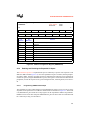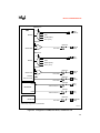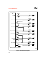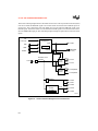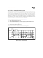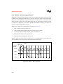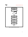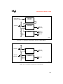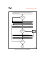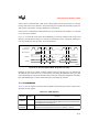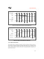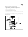
1
Intel386™ EX Embedded Microprocessor User’s Manual title.fm4 Page i Tuesday, August 15, 1995 3:01 PM Intel386™ EX Embedded Microprocessor User’s Manual February 1995 title.fm4 Page ii Tuesday, August 15, 1995 3:01 PM Information in this document is provided solely to enable use of Intel products. Intel assumes no liability whatsoever, including infringement of any patent or copyright, for sale and use of Intel products except as provided in Intel’s Terms and Conditions of Sale for such products. Intel Corporation makes no warranty for the use of its products and assumes no responsibility for any errors which may appear in this document nor does it make a commitment to update the information contained herein. Intel retains the right to make changes to these specifications at any time, without notice. Contact your local Intel sales office or your distributor to obtain the latest specifications before placing your product order. MDS is an ordering code only and is not used as a product name or trademark of Intel Corporation. Intel Corporation and Intel's FASTPATH are not affiliated with Kinetics, a division of Excelan, Inc. or its FASTPATH trademark or products. *Other brands and names are the property of their respective owners. Additional copies of this document or other Intel literature may be obtained from: Intel Corporation Literature Sales P.O. Box 7641 Mt. Prospect, IL 60056-7641 or call 1-800-879-4683 ii CHAPTER 1 GUIDE TO THIS MANUAL 1.1 MANUAL CONTENTS ................................................................................................... 1-1 1.2 NOTATIONAL CONVENTIONS..................................................................................... 1-2 1.3 SPECIAL TERMINOLOGY ............................................................................................ 1-4 1.4 RELATED DOCUMENTS .............................................................................................. 1-5 1.5 CUSTOMER SERVICE.................................................................................................. 1-6 1.5.1 How to Use Intel's FaxBack Service .........................................................................1-6 1.5.2 How to Use Intel's Application BBS ..........................................................................1-7 1.5.3 How to Find the Latest ApBUILDER Files and Hypertext Manuals and Data Sheets on the BBS ............................................................................................1-8 CHAPTER 2 ARCHITECTURAL OVERVIEW 2.1 CORE ............................................................................................................................ 2-1 2.2 INTEGRATED PERIPHERALS...................................................................................... 2-3 2.3 PC COMPATIBILITY...................................................................................................... 2-5 2.3.1 I/O Considerations ....................................................................................................2-5 2.3.2 PC/AT Compatibility ..................................................................................................2-5 2.3.3 Enhanced DMA Controller ........................................................................................2-5 2.3.4 SIO Channels ............................................................................................................2-6 CHAPTER 3 CORE OVERVIEW 3.1 SYSTEM MANAGEMENT MODE OVERVIEW ............................................................. 3-2 3.1.1 SMM Hardware Interface ..........................................................................................3-2 3.1.1.1 SMI# (System Management Interrupt Input) ...................................................3-2 3.1.1.2 SMIACT# (SMM Active Output) .......................................................................3-3 3.1.2 SMI# Interrupt ...........................................................................................................3-3 3.1.3 SMRAM .....................................................................................................................3-5 3.1.4 Chip-select Unit Support for SMRAM ........................................................................3-6 3.1.5 I/O Restart .................................................................................................................3-7 3.1.6 HALT Restart ............................................................................................................3-7 3.1.7 SMRAM State Dump Area ........................................................................................3-8 3.1.8 Resume Instruction (RSM) ......................................................................................3-10 3.1.9 SMM Priority ...........................................................................................................3-10 3.2 SYSTEM MANAGEMENT INTERRUPT...................................................................... 3-10 3.2.1 System Management Interrupt During HALT Cycle ................................................3-12 3.2.2 System Management Interrupt During I/O Instruction .............................................3-13 3.2.3 Interrupt During SMM Handler ................................................................................3-14 3.2.4 SMM Handler Terminated by RESET .....................................................................3-15 3.2.5 HALT During SMM Handler ....................................................................................3-16 iii 3.2.6 SMI# During SMM Operation ..................................................................................3-17 3.3 THE Intel386 EX™ PROCESSOR IDENTIFIER REGISTERS ....................................3-17 CHAPTER 4 SYSTEM REGISTER ORGANIZATION 4.1 OVERVIEW ................................................................................................................... 4-2 4.1.1 Intel386™ Processor Core Architecture Registers ...................................................4-2 4.1.2 Intel386™ EX Processor Peripheral Registers .........................................................4-3 4.2 I/O ADDRESS SPACE FOR PC/AT SYSTEMS ............................................................ 4-3 4.3 EXPANDED I/O ADDRESS SPACE.............................................................................. 4-5 4.4 ORGANIZATION OF PERIPHERAL REGISTERS ........................................................ 4-7 4.5 I/O ADDRESS DECODING TECHNIQUES................................................................... 4-8 4.5.1 Address Configuration Register ................................................................................4-8 4.5.2 Enabling and Disabling the Expanded I/O Space .....................................................4-9 4.5.2.1 Programming REMAPCFG Example ...............................................................4-9 4.6 ADDRESSING MODES ............................................................................................... 4-10 4.6.1 DOS-compatible Mode ............................................................................................4-10 4.6.2 Nonintrusive DOS Mode .........................................................................................4-12 4.6.3 Enhanced DOS Mode .............................................................................................4-12 4.6.4 NonDOS Mode ........................................................................................................4-12 4.7 PERIPHERAL REGISTER ADDRESSES.................................................................... 4-16 CHAPTER 5 DEVICE CONFIGURATION 5.1 INTRODUCTION ........................................................................................................... 5-1 5.2 PERIPHERAL CONFIGURATION ................................................................................. 5-2 5.2.1 DMA Controller, Bus Arbiter, and Refresh Unit Configuration ..................................5-3 5.2.1.1 Using The DMA Unit with External Devices ....................................................5-3 5.2.1.2 DMA Service to an SIO or SSIO Peripheral ....................................................5-4 5.2.1.3 Using The Timer To Initiate DMA Transfers ....................................................5-4 5.2.1.4 Limitations Due To Pin Signal Multiplexing .....................................................5-4 5.2.2 Interrupt Control Unit Configuration ..........................................................................5-7 5.2.3 Timer/Counter Unit Configuration ...........................................................................5-10 5.2.4 Asynchronous Serial I/O Configuration ...................................................................5-12 5.2.5 Serial Synchronous I/O Configuration .....................................................................5-17 5.2.6 Core Configuration ..................................................................................................5-18 5.3 PIN CONFIGURATION................................................................................................ 5-20 5.4 DEVICE CONFIGURATION PROCEDURE ................................................................ 5-25 5.5 CONFIGURATION EXAMPLE..................................................................................... 5-25 5.5.1 Example Design Requirements ...............................................................................5-26 5.5.2 Example Design Solution ........................................................................................5-26 iv CHAPTER 6 CLOCK AND POWER MANAGEMENT UNIT 6.1 OVERVIEW ................................................................................................................... 6-1 6.1.1 Clock Generation Logic .............................................................................................6-1 6.1.2 Power Management Logic ........................................................................................6-3 6.1.2.1 SMM Interaction with Power Management Modes ..........................................6-4 6.1.2.2 Bus Interface Unit Operation During Idle Mode ...............................................6-5 6.1.2.3 Watchdog Timer Unit Operation During Idle Mode ..........................................6-5 6.1.3 Clock and Power Management Registers and Signals .............................................6-5 6.2 CONTROLLING THE PSCLK FREQUENCY ................................................................ 6-6 6.3 CONTROLLING POWER MANAGEMENT MODES ..................................................... 6-8 6.3.1 Idle Mode ..................................................................................................................6-9 6.3.2 Powerdown Mode ...................................................................................................6-10 6.4 DESIGN CONSIDERATIONS...................................................................................... 6-11 6.4.1 Reset Considerations ..............................................................................................6-11 6.4.2 Powerdown Considerations ....................................................................................6-13 CHAPTER 7 BUS INTERFACE UNIT 7.1 OVERVIEW ................................................................................................................... 7-1 7.1.1 Bus Signal Descriptions ............................................................................................7-2 7.2 BUS OPERATION ......................................................................................................... 7-4 7.2.1 Bus States .................................................................................................................7-7 7.2.2 Pipelining ..................................................................................................................7-8 7.2.3 Data Bus Transfers and Operand Alignment ............................................................7-8 7.2.4 Ready Logic ............................................................................................................7-10 7.3 BUS CYCLES .............................................................................................................. 7-12 7.3.1 Read Cycle .............................................................................................................7-12 7.3.2 Write Cycle ..............................................................................................................7-14 7.3.3 Pipelined Cycle .......................................................................................................7-16 7.3.4 Interrupt Acknowledge Cycle ..................................................................................7-19 7.3.5 Halt/Shutdown Cycle ...............................................................................................7-22 7.3.6 Refresh Cycle .........................................................................................................7-24 7.3.7 BS8 Cycle ...............................................................................................................7-27 7.4 BUS LOCK................................................................................................................... 7-29 7.4.1 Locked Cycle Activators ..........................................................................................7-29 7.4.2 Locked Cycle Timing ...............................................................................................7-29 7.4.3 LOCK# Signal Duration ...........................................................................................7-30 7.5 HOLD/HLDA (HOLD ACKNOWLEDGE)...................................................................... 7-30 7.5.1 HOLD/HLDA Timing ................................................................................................7-31 7.5.2 HOLD Signal Latency .............................................................................................7-33 v CHAPTER 8 INTERRUPT CONTROL UNIT 8.1 OVERVIEW ................................................................................................................... 8-1 8.2 ICU OPERATION........................................................................................................... 8-4 8.2.1 Interrupt Sources ......................................................................................................8-4 8.2.2 Interrupt Priority ........................................................................................................8-5 8.2.2.1 Assigning an Interrupt Level ............................................................................8-5 8.2.2.2 Determining Priority .........................................................................................8-6 8.2.3 Interrupt Vectors .......................................................................................................8-7 8.2.4 Interrupt Process .......................................................................................................8-8 8.2.5 Poll Mode ................................................................................................................8-12 8.3 PROGRAMMING ......................................................................................................... 8-13 8.3.1 Port 3 Configuration Register (P3CFG) ..................................................................8-15 8.3.2 Interrupt Configuration Register (INTCFG) .............................................................8-16 8.3.3 Initialization Command Word 1 (ICW1) ...................................................................8-17 8.3.4 Initialization Command Word 2 (ICW2) ...................................................................8-18 8.3.5 Initialization Command Word 3 (ICW3) ...................................................................8-19 8.3.6 Initialization Command Word 4 (ICW4) ...................................................................8-21 8.3.7 Operation Command Word 1 (OCW1) ....................................................................8-22 8.3.8 Operation Command Word 2 (OCW2) ....................................................................8-23 8.3.9 Operation Command Word 3 (OCW3) ....................................................................8-24 8.3.10 Poll Status Byte (POLL) ..........................................................................................8-25 8.3.11 Programming Considerations ..................................................................................8-25 8.4 DESIGN CONSIDERATIONS...................................................................................... 8-26 8.4.1 Interrupt Acknowledge Cycle ..................................................................................8-26 8.4.2 Interrupt Detection ..................................................................................................8-27 8.4.3 Spurious Interrupts ..................................................................................................8-28 8.4.4 Interrupt Timing .......................................................................................................8-28 CHAPTER 9 TIMER/COUNTER UNIT 9.1 OVERVIEW ................................................................................................................... 9-1 9.1.1 TCU Signals and Registers .......................................................................................9-2 9.2 TCU OPERATION ......................................................................................................... 9-4 9.2.1 Mode 0 – Interrupt on Terminal Count ......................................................................9-6 9.2.2 Mode 1 – Hardware Retriggerable One-shot ............................................................9-8 9.2.3 Mode 2 – Rate Generator .......................................................................................9-10 9.2.4 Mode 3 – Square Wave ..........................................................................................9-12 9.2.5 Mode 4 – Software-triggered Strobe .......................................................................9-16 9.2.6 Mode 5 – Hardware-triggered Strobe ......................................................................9-18 9.3 PROGRAMMING ......................................................................................................... 9-20 9.3.1 Configuring the Input and Output Signals ...............................................................9-20 9.3.2 Initializing the Counters ...........................................................................................9-25 vi 9.3.3 Writing the Counters ...............................................................................................9-27 9.3.4 Reading the Counter ...............................................................................................9-28 9.3.4.1 Simple Read ..................................................................................................9-28 9.3.4.2 Counter-latch Command ...............................................................................9-29 9.3.4.3 Read-back Command ...................................................................................9-31 9.3.5 Programming Considerations ..................................................................................9-34 CHAPTER 10 WATCHDOG TIMER UNIT 10.1 OVERVIEW ................................................................................................................. 10-1 10.1.1 WDT Operation .......................................................................................................10-2 10.1.2 WDT Registers and Signals ....................................................................................10-3 10.2 PROGRAMMING THE WDT........................................................................................ 10-5 10.2.1 General-purpose Timer Mode .................................................................................10-7 10.2.2 Software Watchdog Mode .......................................................................................10-8 10.2.3 Bus Monitor Mode ...................................................................................................10-8 10.3 DISABLING THE WDT ................................................................................................ 10-9 10.4 DESIGN CONSIDERATIONS...................................................................................... 10-9 CHAPTER 11 ASYNCHRONOUS SERIAL I/O UNIT 11.1 OVERVIEW ................................................................................................................. 11-1 11.1.1 SIO Signals .............................................................................................................11-3 11.2 SIO OPERATION ........................................................................................................ 11-3 11.2.1 Baud-rate Generator ...............................................................................................11-4 11.2.2 Transmitter ..............................................................................................................11-5 11.2.3 Receiver ..................................................................................................................11-8 11.2.4 Modem Control .....................................................................................................11-10 11.2.5 Diagnostic Mode ...................................................................................................11-10 11.2.6 SIO Interrupt Sources ...........................................................................................11-11 11.3 PROGRAMMING ....................................................................................................... 11-12 11.3.1 Pin and Port Configuration Registers (PINCFG and PnCFG [n = 1–3]) ................11-14 11.3.2 SIO and SSIO Configuration Register (SIOCFG) .................................................11-18 11.3.3 Divisor Latch Registers (DLLn and DLHn) ............................................................11-19 11.3.4 Transmit Buffer Register (TBRn) ...........................................................................11-20 11.3.5 Receive Buffer Register (RBRn) ...........................................................................11-21 11.3.6 Serial Line Control Register (LCRn) ......................................................................11-22 11.3.7 Serial Line Status Register (LSRn) .......................................................................11-23 11.3.8 Interrupt Enable Register (IERn) ...........................................................................11-24 11.3.9 Interrupt ID Register (IIRn) ....................................................................................11-25 11.3.10 Modem Control Register (MCRn) ..........................................................................11-26 11.3.11 Modem Status Register (MSRn) ...........................................................................11-28 vii 11.3.12 Scratch Pad Register (SCRn) ...............................................................................11-29 11.4 PROGRAMMING CONSIDERATIONS...................................................................... 11-29 CHAPTER 12 SYNCHRONOUS SERIAL I/O UNIT 12.1 OVERVIEW ................................................................................................................. 12-1 12.1.1 SSIO Signals ...........................................................................................................12-4 12.2 SSIO OPERATION ...................................................................................................... 12-4 12.2.1 Baud-rate Generator ...............................................................................................12-4 12.2.2 Transmitter ..............................................................................................................12-6 12.2.3 Receiver ..................................................................................................................12-9 12.3 PROGRAMMING ....................................................................................................... 12-11 12.3.1 Pin Configuration Register (PINCFG) ...................................................................12-13 12.3.2 SIO and SSIO Configuration Register (SIOCFG) .................................................12-14 12.3.3 Prescale Clock Register (CLKPRS) ......................................................................12-15 12.3.4 SSIO Baud-rate Control Register (SSIOBAUD) ....................................................12-16 12.3.5 SSIO Baud-rate Count Down Register (SSIOCTR) ..............................................12-17 12.3.6 SSIO Control 1 Register (SSIOCON1) ..................................................................12-18 12.3.7 SSIO Control 2 Register (SSIOCON2) ..................................................................12-20 12.3.8 SSIO Transmit Holding Buffer (SSIOTBUF) .........................................................12-21 12.3.9 SSIO Receive Holding Buffer (SSIORBUF) ..........................................................12-22 12.4 DESIGN CONSIDERATIONS.................................................................................... 12-22 CHAPTER 13 INPUT/OUTPUT PORTS 13.1 OVERVIEW ................................................................................................................. 13-1 13.2 PROGRAMMING ......................................................................................................... 13-4 13.2.1 Pin Configuration ....................................................................................................13-4 13.2.2 Initialization Sequence ............................................................................................13-7 13.3 DESIGN CONSIDERATIONS...................................................................................... 13-7 13.3.1 Pin Status During and After Reset ..........................................................................13-8 CHAPTER 14 CHIP-SELECT UNIT 14.1 OVERVIEW ................................................................................................................. 14-1 14.2 CSU OPERATION ....................................................................................................... 14-1 14.2.1 Defining a Channel’s Address Block .......................................................................14-1 14.2.2 System Management Mode Support ......................................................................14-7 14.2.3 Bus Cycle Length Control .......................................................................................14-7 14.2.4 Bus Size Control .....................................................................................................14-7 14.2.5 Overlapping Regions ..............................................................................................14-8 14.3 PROGRAMMING ......................................................................................................... 14-9 14.3.1 Pin Configuration Register (PINCFG) ...................................................................14-11 viii 14.3.2 14.3.3 14.3.4 14.3.5 Port 2 Configuration Register (P2CFG) ................................................................14-12 Chip-select Address Registers ..............................................................................14-13 Chip-select Mask Registers ..................................................................................14-15 Programming Considerations ................................................................................14-16 CHAPTER 15 REFRESH CONTROL UNIT 15.1 DYNAMIC MEMORY CONTROL................................................................................. 15-1 15.2 RCU OVERVIEW......................................................................................................... 15-1 15.2.1 RCU Signals ...........................................................................................................15-3 15.2.2 Refresh Intervals .....................................................................................................15-3 15.2.3 Refresh Addresses .................................................................................................15-4 15.2.4 Refresh Methods .....................................................................................................15-4 15.2.5 Bus Arbitration ........................................................................................................15-4 15.3 RCU OPERATION ....................................................................................................... 15-5 15.4 PROGRAMMING ......................................................................................................... 15-6 15.4.1 Refresh Clock Interval Register (RFSCIR) ..............................................................15-7 15.4.2 Refresh Control Register (RFSCON) ......................................................................15-8 15.4.3 Refresh Base Address Register (RFSBAD) ............................................................15-9 15.4.4 Refresh Address Register (RFSADD) ...................................................................15-10 15.5 DESIGN CONSIDERATIONS.................................................................................... 15-10 CHAPTER 16 DMA CONTROLLER 16.1 OVERVIEW ................................................................................................................. 16-1 16.1.1 DMA Signals ...........................................................................................................16-3 16.2 DMA OPERATION....................................................................................................... 16-3 16.2.1 DMA Transfers ........................................................................................................16-3 16.2.2 Bus Cycle Options for Data Transfers .....................................................................16-4 16.2.3 Starting DMA Transfers ..........................................................................................16-5 16.2.4 Bus Control Arbitration ............................................................................................16-6 16.2.5 Ending DMA Transfers ............................................................................................16-6 16.2.6 Buffer-transfer Modes .............................................................................................16-7 16.2.7 Data-transfer Modes ...............................................................................................16-8 16.2.7.1 Single Data-transfer Mode ............................................................................16-9 16.2.7.2 Block Data-transfer Mode ............................................................................16-13 16.2.7.3 Demand Data-transfer Mode .......................................................................16-16 16.2.8 Cascade Mode ......................................................................................................16-20 16.2.9 DMA Interrupts ......................................................................................................16-21 16.2.10 8237A Compatibility ..............................................................................................16-22 16.3 PROGRAMMING ....................................................................................................... 16-23 16.3.1 Pin Configuration Register (PINCFG) ...................................................................16-26 16.3.2 DMA Configuration Register (DMACFG) ..............................................................16-27 ix 16.3.3 16.3.4 16.3.5 16.3.6 16.3.7 16.3.8 16.3.9 16.3.10 16.3.11 16.3.12 16.3.13 16.3.14 16.3.15 16.3.16 16.3.17 Channel Registers ................................................................................................16-28 Overflow Enable Register (DMAOVFE) ................................................................16-29 Command 1 Register (DMACMD1) .......................................................................16-30 Status Register (DMASTS) ...................................................................................16-31 Command 2 Register (DMACMD2) .......................................................................16-32 Mode 1 Register (DMAMOD1) ..............................................................................16-33 Mode 2 Register (DMAMOD2) ..............................................................................16-34 Software Request Register (DMASRR) ................................................................16-36 Channel Mask and Group Mask Registers (DMAMSK and DMAGRPMSK) .........16-38 Bus Size Register (DMABSR) ...............................................................................16-39 Chaining Register (DMACHR) ..............................................................................16-40 Interrupt Enable Register (DMAIEN) .....................................................................16-41 Interrupt Status Register (DMAIS) ........................................................................16-42 Software Commands ............................................................................................16-43 Programming Considerations ................................................................................16-44 CHAPTER 17 JTAG TEST-LOGIC UNIT 17.1 OVERVIEW ................................................................................................................. 17-1 17.2 TEST-LOGIC UNIT OPERATION................................................................................ 17-3 17.2.1 Test Access Port (TAP) ..........................................................................................17-3 17.2.2 Test Access Port (TAP) Controller ..........................................................................17-4 17.2.3 Instruction Register (IR) ..........................................................................................17-7 17.2.4 Data Registers ........................................................................................................17-8 17.3 TESTING ................................................................................................................... 17-10 17.3.1 Identifying the Device ............................................................................................17-11 17.3.2 Bypassing Devices on a Board .............................................................................17-11 17.3.3 Sampling Device Operation and Preloading Data .................................................17-11 17.3.4 Testing the Device ................................................................................................17-12 17.3.5 Testing the Interconnections .................................................................................17-12 17.3.6 Disabling the Output Drivers .................................................................................17-12 17.4 TIMING INFORMATION ............................................................................................ 17-13 17.5 DESIGN CONSIDERATIONS.................................................................................... 17-15 APPENDIX A SIGNAL DESCRIPTIONS APPENDIX B COMPATIBILITY WITH PC/AT* ARCHITECTURE B.1 DEPARTURES FROM PC/AT* SYSTEM ARCHITECTURE........................................ B-1 B.1.1 DMA Unit ................................................................................................................ B-1 B.1.2 Bus Signals ............................................................................................................. B-2 B.1.3 Interrupt Control Unit .............................................................................................. B-4 B.1.4 SIO Units ................................................................................................................ B-4 x B.1.5 B.1.6 B.1.7 Word Read/Write Access of 8-bit Registers ............................................................ B-4 CPU-only Reset ...................................................................................................... B-4 HOLD, HLDA Pins .................................................................................................. B-5 GLOSSARY INDEX xi CONTENTS FIGURES Figure 2-1 3-1 3-2 3-3 3-4 3-5 3-6 3-7 3-8 4-1 4-2 4-3 4-4 4-5 4-6 4-7 4-8 5-1 5-2 5-3 5-4 5-5 5-6 5-7 5-8 5-9 5-10 5-11 5-12 5-13 5-14 5-15 5-16 5-17 5-18 5-19 5-20 5-21 5-22 6-1 6-2 6-3 6-4 6-5 xii Page Intel386™ EX Processor Block Diagram......................................................................2-2 Standard SMI# ...........................................................................................................3-11 SMIACT# Latency ......................................................................................................3-12 SMI# During HALT .....................................................................................................3-13 SMI# During I/O Instruction ........................................................................................3-13 SMI# Timing ...............................................................................................................3-14 Interrupted SMI# Service............................................................................................3-15 SMI# Service Terminated by RESET .........................................................................3-16 HALT During SMM Handler........................................................................................3-17 PC/AT I/O Address Space............................................................................................4-4 Expanded I/O Address Space ......................................................................................4-6 Address Configuration Register (REMAPCFG)............................................................4-9 Programming the ESE Bit ..........................................................................................4-10 DOS-Compatible Mode ..............................................................................................4-11 Example of Nonintrusive DOS-Compatible Mode ......................................................4-13 Enhanced DOS Mode ................................................................................................4-14 NonDOS Mode ...........................................................................................................4-15 Peripheral and Pin Connections...................................................................................5-2 Configuration of DMA, Bus Arbiter, and Refresh Unit ..................................................5-5 DMA Configuration Register.........................................................................................5-6 Interrupt Control Unit Configuration..............................................................................5-8 Interrupt Configuration Register ...................................................................................5-9 Timer/Counter Unit Configuration...............................................................................5-11 Timer Configuration Register......................................................................................5-12 Serial I/O Unit 0 Configuration....................................................................................5-14 Serial I/O Unit 1 Configuration....................................................................................5-15 SIO and SSIO Configuration Register ........................................................................5-16 SSIO Unit Configuration .............................................................................................5-17 Core Configuration .....................................................................................................5-18 Port 92 Configuration Register ...................................................................................5-19 Pin Configuration Register .........................................................................................5-21 Port 1 Configuration Register .....................................................................................5-22 Port 2 Configuration Register .....................................................................................5-23 Port 3 Configuration Register .....................................................................................5-24 Abbreviated Pin Configuration Register Tables..........................................................5-27 Abbreviated Peripheral Configuration Register Tables ..............................................5-28 Peripheral and Pin Connections for the Example Design...........................................5-29 Pin Configuration Worksheet......................................................................................5-30 Peripheral Configuration Worksheet...........................................................................5-31 Clock and Power Management Unit Connections ........................................................6-2 Clock Synchronization ..................................................................................................6-3 SMM Interaction with Idle and Powerdown Modes.......................................................6-4 Clock Prescale Register (CLKPRS) .............................................................................6-7 PSCLK Divider Circuitry ...............................................................................................6-8 CONTENTS FIGURES Figure 6-6 6-7 6-8 6-9 6-10 7-1 7-2 7-3 7-4 7-5 7-6 7-7 7-8 7-9 7-10 7-11 7-12 7-13 7-14 8-1 8-2 8-3 8-4 8-5 8-6 8-7 8-8 8-9 8-10 8-11 8-12 8-13 8-14 8-15 8-16 8-17 8-18 9-1 9-2 9-3 9-4 9-5 9-6 9-7 Page Power Control Register (PWRCON).............................................................................6-9 Timing Diagram, Entering and Leaving Idle Mode .....................................................6-10 Timing Diagram, Entering and Leaving Powerdown Mode ........................................6-11 Reset Synchronization Circuit ....................................................................................6-12 Phase Clock Generator ..............................................................................................6-13 Basic External Bus Cycles............................................................................................7-6 Bus State Diagram (Does Not Include Address Pipelining)..........................................7-8 Ready Logic ...............................................................................................................7-10 Basic Internal and External Bus Cycles......................................................................7-11 Nonpipelined Address Read Cycle.............................................................................7-13 Nonpipelined Address Write Cycles ...........................................................................7-15 Pipelined Address Cycles...........................................................................................7-17 Interrupt Acknowledge Cycles ....................................................................................7-21 Halt Cycle ...................................................................................................................7-23 Basic Refresh Cycle ...................................................................................................7-25 Refresh Cycle During HOLD/HLDA............................................................................7-26 BS8 Cycle...................................................................................................................7-28 LOCK# Signal During Address Pipelining ..................................................................7-30 Complete Bus States (Including Pipelined Address) ..................................................7-32 Interrupt Unit Connections............................................................................................8-3 Methods for Changing the Default Interrupt Structure..................................................8-6 Interrupt Process – Master Request from Non-slave Source .......................................8-9 Interrupt Process – Slave Request.............................................................................8-10 Interrupt Process – Master Request from Slave Source ............................................8-11 Port 3 Configuration Register (P3CFG)......................................................................8-15 Interrupt Configuration Register (INTCFG).................................................................8-16 Initialization Command Word 1 Register (ICW1)........................................................8-17 Initialization Command Word 2 Register (ICW2)........................................................8-18 Initialization Command Word 3 Register (ICW3 – Master).........................................8-19 Initialization Command Word 3 Register (ICW3 – Slave)...........................................8-20 Initialization Command Word 4 Register (ICW4)........................................................8-21 Operation Command Word 1 (OCW1) .......................................................................8-22 Operation Command Word 2 (OCW2) .......................................................................8-23 Operation Command Word 3 (OCW3) .......................................................................8-24 Poll Status Byte (POLL) .............................................................................................8-25 Interrupt Acknowledge Cycle......................................................................................8-26 Spurious Interrupts .....................................................................................................8-28 Timer/Counter Unit Block Diagram...............................................................................9-2 Mode 0 – Basic Operation ............................................................................................9-6 Mode 0 – Disabling the Count ......................................................................................9-7 Mode 0 – Writing a New Count.....................................................................................9-7 Mode 1 – Basic Operation ............................................................................................9-8 Mode 1 – Retriggering the One-shot ............................................................................9-9 Mode 1 – Writing a New Count.....................................................................................9-9 xiii CONTENTS FIGURES Figure 9-8 9-9 9-10 9-11 9-12 9-13 9-14 9-15 9-16 9-17 9-18 9-19 9-20 9-21 9-22 9-23 9-24 9-25 9-26 9-27 9-28 9-29 9-30 9-31 10-1 10-2 10-3 10-4 11-1 11-2 11-3 11-4 11-5 11-6 11-7 11-8 11-9 11-10 11-11 11-12 11-13 11-14 11-15 11-16 xiv Page Mode 2 – Basic Operation ..........................................................................................9-10 Mode 2 – Disabling the Count ....................................................................................9-11 Mode 2 – Writing a New Count...................................................................................9-11 Mode 3 – Basic Operation (Even Count)....................................................................9-12 Mode 3 – Basic Operation (Odd Count) .....................................................................9-13 Mode 3 – Disabling the Count ....................................................................................9-14 Mode 3 – Writing a New Count (With a Trigger).........................................................9-14 Mode 3 – Writing a New Count (Without a Trigger)....................................................9-15 Mode 4 – Basic Operation ..........................................................................................9-16 Mode 4 – Disabling the Count ....................................................................................9-17 Mode 4 – Writing a New Count...................................................................................9-17 Mode 5 – Basic Operation ..........................................................................................9-18 Mode 5 – Retriggering the Strobe ..............................................................................9-19 Mode 5 – Writing a New Count...................................................................................9-19 Timer Configuration Register (TMRCFG)...................................................................9-21 Timer/Counter Unit Signal Connections .....................................................................9-22 Port 3 Configuration Register (P3CFG)......................................................................9-23 Pin Configuration Register (PINCFG).........................................................................9-24 Timer Control Register (Control Word Format) ..........................................................9-26 Timer n Register (Write Format).................................................................................9-27 Timer Control Register (Counter-latch Format) ..........................................................9-29 Timer n Register (Read Format).................................................................................9-30 Timer Control Register (Read-back Format) ..............................................................9-31 Timer n Register (Status Format)...............................................................................9-33 Watchdog Timer Unit Connections.............................................................................10-2 WDT Counter Value Registers (WDTCNTH and WDTCNTL) ....................................10-5 WDT Status Register (WDTSTATUS) ........................................................................10-6 WDT Reload Value Registers (WDTRLDH and WDTRLDL)......................................10-7 SIO0 and SIO1 Connections ......................................................................................11-2 SIOn Baud-rate Generator Clock Sources .................................................................11-4 SIOn Transmitter ........................................................................................................11-6 SIOn Data Transmission Process Flow......................................................................11-7 SIOn Receiver ............................................................................................................11-8 SIOn Data Reception Process Flow ...........................................................................11-9 Pin Configuration Register (PINCFG).......................................................................11-14 Port 1 Configuration Register (P1CFG)....................................................................11-15 Port 2 Configuration Register (P2CFG)....................................................................11-16 Port 3 Configuration Register (P3CFG)....................................................................11-17 SIO and SSIO Configuration Register (SIOCFG).....................................................11-18 Divisor Latch Registers (DLLn and DLHn) ...............................................................11-19 Transmit Buffer Register (TBRn) ..............................................................................11-20 Receive Buffer Register (RBRn)...............................................................................11-21 Serial Line Control Register (LCRn) .........................................................................11-22 Serial Line Status Register (LSRn)...........................................................................11-23 CONTENTS FIGURES Figure 11-17 11-18 11-19 11-20 11-21 11-22 11-23 12-1 12-2 12-3 12-4 12-5 12-6 12-7 12-8 12-9 12-10 12-11 12-12 12-13 12-14 12-15 12-16 12-17 12-18 12-19 13-1 13-2 13-3 13-4 13-5 14-1 14-2 14-3 14-4 14-5 14-6 14-7 14-8 14-9 15-1 15-2 15-3 15-4 Page Interrupt Enable Register (IERn) ..............................................................................11-24 Interrupt ID Register (IIRn) .......................................................................................11-25 Modem Control Signals – Diagnostic Mode Connections ........................................11-26 Modem Control Signals – Internal Connections .......................................................11-26 Modem Control Register (MCRn) .............................................................................11-27 Modem Status Register (MSRn)...............................................................................11-28 Scratch Pad Register (SCRn)...................................................................................11-29 Transmitter and Receiver in Master Mode .................................................................12-2 Transmitter in Master Mode, Receiver in Slave Mode................................................12-2 Transmitter in Slave Mode, Receiver in Master Mode................................................12-3 Transmitter and Receiver in Slave Mode ...................................................................12-3 Clock Sources for the Baud-rate Generator ...............................................................12-5 Process Flow for Transmitting Data ...........................................................................12-7 Transmitter Master Mode, Single Word Transfer (Enabled when Clock is High) .......12-8 Transmitter Master Mode, Single Word Transfer (Enabled when Clock is Low) ........12-8 Process Flow for Receiving Data .............................................................................12-10 Receiver Master Mode, Single Word Transfer .........................................................12-11 Pin Configuration Register (PINCFG).......................................................................12-13 SIO and SSIO Configuration Register (SIOCFG).....................................................12-14 Clock Prescale Register (CLKPRS) .........................................................................12-15 SSIO Baud-rate Control Register (SSIOBAUD) .......................................................12-16 SSIO Baud-rate Count Down Register (SSIOCTR)..................................................12-17 SSIO Control 1 Register (SSIOCON1) .....................................................................12-19 SSIO Control 2 Register (SSIOCON2) .....................................................................12-20 SSIO Transmit Holding Buffer (SSIOTBUF).............................................................12-21 SSIO Receive Holding Buffer (SSIORBUF) .............................................................12-22 I/O Port Block Diagram...............................................................................................13-2 Port Mode Configuration Register (PnCFG)...............................................................13-5 Port Direction Register (PnDIR) .................................................................................13-5 Port Data Latch Register (PnLTC),.............................................................................13-6 Port Pin State Register (PnPIN) .................................................................................13-6 Channel Address Comparison Logic ..........................................................................14-2 Determining a Channel’s Address Block Size ............................................................14-2 Bus Cycle Length Adjustments for Overlapping Regions...........................................14-8 Pin Configuration Register (PINCFG).......................................................................14-11 Port 2 Configuration Register (P2CFG)....................................................................14-12 Chip-select High Address Register (CSnADH, UCSADH) .......................................14-13 Chip-select Low Address Register (CSnADL, UCSADL) .........................................14-14 Chip-select High Mask Registers (CSnMSKH, UCSMSKH).....................................14-15 Chip-select Low Mask Registers (CSnMSKL, UCSMSKL).......................................14-16 Refresh Control Unit Connections ..............................................................................15-2 Refresh Clock Interval Register (RFSCIR) .................................................................15-7 Refresh Control Register (RFSCON) .........................................................................15-8 Refresh Base Address Register (RFSBAD) ...............................................................15-9 xv CONTENTS FIGURES Figure 15-5 16-1 16-2 16-3 16-4 16-5 16-6 16-7 16-8 16-9 16-10 16-11 16-12 16-13 16-14 16-15 16-16 16-17 16-18 16-19 16-20 16-21 16-22 16-23 16-24 16-25 16-26 16-27 16-28 16-29 16-30 16-31 16-32 17-1 17-2 17-3 17-4 17-5 17-6 B-1 B-2 xvi Page Refresh Address Register (RFSADD) ......................................................................15-10 DMA Unit Block Diagram............................................................................................16-2 DMA Transfer Started by DRQn.................................................................................16-5 Changing the Priority of the DMA Channel and External Bus Requests ....................16-6 Buffer Transfer Ended by an Expired Byte Count ......................................................16-7 Buffer Transfer Ended by the EOP# Input..................................................................16-7 Single Data-transfer Mode with Single Buffer-transfer Mode ...................................16-10 Single Data-transfer Mode with Autoinitialize Buffer-transfer Mode .........................16-11 Single Data-transfer Mode with Chaining Buffer-transfer Mode ...............................16-12 Block Data-transfer Mode with Single Buffer-transfer Mode ....................................16-14 Block Data-transfer Mode with Autoinitialize Buffer-transfer Mode ..........................16-15 Buffer Transfer Suspended by the Deactivation of DRQn........................................16-16 Demand Data-transfer Mode with Single Buffer-transfer Mode................................16-17 Demand Data-transfer Mode with Autoinitialize Buffer-transfer Mode .....................16-18 Demand Data-transfer Mode with Chaining Buffer-transfer Mode ...........................16-19 Cascade Mode .........................................................................................................16-21 Pin Configuration Register (PINCFG).......................................................................16-26 DMA Configuration Register (DMACFG)..................................................................16-27 DMA Channel Address and Byte Count Registers ...................................................16-28 DMA Overflow Enable Register (DMAOVFE)...........................................................16-29 DMA Command 1 Register (DMACMD1) .................................................................16-30 DMA Status Register (DMASTS)..............................................................................16-31 DMA Command 2 Register (DMACMD2) .................................................................16-32 DMA Mode 1 Register (DMAMOD1) ........................................................................16-33 DMA Mode 2 Register (DMAMOD2) ........................................................................16-35 DMA Software Request Register (DMASRR – write format)....................................16-36 DMA Software Request Register (DMASRR – read format) ....................................16-37 DMA Channel Mask Register (DMAMSK) ................................................................16-38 DMA Group Channel Mask Register (DMAGRPMSK) .............................................16-38 DMA Bus Size Register (DMABSR) .........................................................................16-39 DMA Chaining Register (DMACHR).........................................................................16-40 DMA Interrupt Enable Register (DMAIEN) ...............................................................16-41 DMA Interrupt Status Register (DMAIS)...................................................................16-42 Test Logic Unit Connections ......................................................................................17-2 TAP Controller (Finite-State Machine)........................................................................17-6 Instruction Register (IR)..............................................................................................17-7 Identification Code Register (IDCODE) ......................................................................17-9 Internal and External Timing for Loading the Instruction Register............................17-13 Internal and External Timing for Loading a Data Register........................................17-14 Derivation of AEN Signal in a Typical PC/AT System ................................................. B-3 Derivation of AEN Signal for Intel386™ EX Processor-based Systems...................... B-3 CONTENTS TABLES Table 2-1 2-2 3-1 4-1 4-2 5-1 6-1 6-2 7-1 7-2 7-3 8-1 8-2 9-1 9-2 9-3 9-4 9-5 10-1 10-2 11-1 11-2 11-3 11-4 11-5 11-6 12-1 12-2 12-3 13-1 13-2 13-3 13-4 14-1 14-2 15-1 15-2 16-1 16-2 16-3 17-1 17-2 17-3 17-4 Page PC-compatible Peripherals...........................................................................................2-3 Embedded Application-specific Peripherals .................................................................2-4 Relative Priority of Exceptions and Interrupts.............................................................3-10 Peripheral Register I/O Address Map in Slot 15...........................................................4-7 Peripheral Register Addresses...................................................................................4-16 Signal Pairs on Pins without Multiplexers...................................................................5-20 Clock and Power Management Registers ....................................................................6-5 Clock and Power Management Signals........................................................................6-5 Bus Interface Unit Signals ............................................................................................7-2 Bus Status Definitions ..................................................................................................7-4 Sequence of Misaligned Bus Transfers........................................................................7-9 82C59A Master and Slave Interrupt Sources ...............................................................8-4 ICU Registers .............................................................................................................8-13 TCU Signals .................................................................................................................9-2 TCU Registers..............................................................................................................9-3 Operations Caused by GATEn .....................................................................................9-5 Minimum and Maximum Initial Counts........................................................................9-27 Results of Multiple Read-back Commands Without Reads........................................9-34 WDT Registers ...........................................................................................................10-3 WDT Signals ..............................................................................................................10-4 SIO Signals ................................................................................................................11-3 Maximum and Minimum Output Baud Rates..............................................................11-5 Divisor Values for Common Baud Rates ....................................................................11-5 Status Signal Priorities and Sources ........................................................................11-11 SIO Registers ...........................................................................................................11-12 Access to Multiplexed Registers...............................................................................11-13 SSIO Signals ..............................................................................................................12-4 Maximum and Minimum Baud-rate Output Frequencies ............................................12-6 SSIO Registers.........................................................................................................12-11 Pin Multiplexing ..........................................................................................................13-3 I/O Port Registers.......................................................................................................13-4 Control Register Values for I/O Port Pin Configurations.............................................13-4 Pin Reset Status.........................................................................................................13-8 CSU Signals ...............................................................................................................14-9 CSU Registers............................................................................................................14-9 Refresh Control Unit Signals ......................................................................................15-3 Refresh Control Unit Registers...................................................................................15-6 DMA Signals...............................................................................................................16-3 DMA Registers .........................................................................................................16-23 DMA Software Commands .......................................................................................16-43 Test Access Port Dedicated Pins ...............................................................................17-3 TAP Controller State Descriptions..............................................................................17-4 Example TAP Controller State Selections ..................................................................17-5 Test-logic Unit Instructions .........................................................................................17-7 xvii CONTENTS TABLES Table 17-5 A-1 A-2 A-3 A-4 xviii Page Boundary-scan Register Bit Assignments ................................................................17-10 Signal Description Abbreviations................................................................................. A-1 Signal Descriptions...................................................................................................... A-2 Pin State Abbreviations ............................................................................................... A-7 Pin States After Reset and During Idle, Powerdown, and Hold................................... A-8 CHAPTER 1 GUIDE TO THIS MANUAL This manual describes the embedded Intel386™ EX microprocessor. It is intended for use by hardware designers familiar with the principles of microprocessors and with the Intel386 architecture. 1.1 MANUAL CONTENTS This manual contains 17 chapters and 2 appendixes, a glossary, and an index. This chapter, Chapter 1, provides an overview of the manual. This section summarizes the contents of the remaining chapters and appendixes. The remainder of this chapter describes notational conventions and special terminology used throughout the manual and provides references to related documentation. Chapter 2 — Architectural Overview — describes the device features and some potential applications. Chapter 3 — Core Overview — describes the differences between this device and the Intel386 SX processor core and discusses Intel’s System Management Mode (SMM). Chapter 4 — System Register Organization — describes the organization of the system registers, the I/O address space, address decoding, and addressing modes. Chapter 5 — Device Configuration — explains how to configure the device for various applications. Chapter 6 — Clock and Power Management Unit — describes the clock generation circuitry, power management modes, and system reset logic. Chapter 7 — Bus Interface Unit — describes the bus interface logic, bus states, bus cycles, and instruction pipelining. Chapter 8 — Interrupt Control Unit — describes the interrupt sources and priority options and explains how to program the interrupt control unit. Chapter 9 — Timer/Counter Unit — describes the timer/counters and their available count formats and operating modes. Chapter 10 — Watchdog Timer Unit — explains how to use the watchdog timer unit as a software watchdog, bus monitor, or general-purpose timer. 1-1 GUIDE TO THIS MANUAL Chapter 11 — Asynchronous Serial I/O (SIO) Unit — explains how to use the universal asynchronous receiver/transmitters (UARTs) to transmit and receive serial data. Chapter 12 — Synchronous Serial I/O (SSIO) Unit — explains how to transmit and receive data synchronously. Chapter 13 — Input/Output Ports — describes the general-purpose I/O ports and explains how to configure each pin to serve either as an I/O pin or as a pin controlled by an internal peripheral. Chapter 14 — Chip-select Unit — explains how to use the chip-select channels to access various external memory and I/O devices. Chapter 15 — Refresh Control Unit — describes how the refresh control unit generates periodic refresh requests and refresh addresses to simplify the interface to dynamic memory devices. Chapter 16 — DMA Controller — describes how the enhanced direct memory access controller allows internal and external devices to transfer data directly to and from the system and explains how bus control is arbitrated. Chapter 17 — JTAG Test-logic Unit — describes the independent test-logic unit and explains how to test the device logic and board-level connections. Appendix A — Signal Descriptions — describes the device pins and signals and lists pin states after a system reset and during powerdown, idle, and hold. Appendix B — Compatibility with PC/AT* Architecture — describes the ways in which the device is compatible with the standard PC/AT architecture and the ways in which it departs from the standard. Glossary — defines terms with special meaning used throughout this manual. Index — lists key topics with page number references. 1.2 NOTATIONAL CONVENTIONS The following notations are used throughout this manual. # The pound symbol (#) appended to a signal name indicates that the signal is active low. italics Italics identify variables and introduce new terminology. The context in which italics are used distinguishes between the two possible meanings. Variables must be replaced with correct values. 1-2 GUIDE TO THIS MANUAL Instructions Instruction mnemonics are shown in upper case to avoid confusion. You may use either upper case or lower case. Numbers Hexadecimal numbers are represented by a string of hexadecimal digits followed by the character H. A zero prefix is added to numbers that begin with A through F. (For example, FF is shown as 0FFH.) Decimal and binary numbers are represented by their customary notations. (That is, 255 is a decimal number and 1111 1111 is a binary number. In some cases, the letter B is added for clarity.) Units of Measure The following abbreviations are used to represent units of measure: A Kbyte KΩ mA Mbyte MHz ms mW ns pF W V µA µF µs µW amps, amperes kilobytes kilo-ohms milliamps, milliamperes megabytes megahertz milliseconds milliwatts nanoseconds picofarads watts volts microamps, microamperes microfarads microseconds microwatts Register Bits Bit locations are indexed by 0–7 (or 0–15), where bit 0 is the leastsignificant bit and 7 (or 15) is the most-significant bit. Register Names Register names are shown in upper case. If a register name contains a lowercase, italic character, it represents more than one register. For example, PnCFG represents three registers: P1CFG, P2CFG, and P3CFG. Signal Names Signal names are shown in upper case. When several signals share a common name, an individual signal is represented by the signal name followed by a number, while the group is represented by the signal name followed by a variable (n). For example, the lower chip-select signals are named CS0#, CS1#, CS2#, and so on; they are collectively called CSn#. A pound symbol (#) appended to a signal name identifies an active-low signal. Port pins are represented by the port abbreviation, a period, and the pin number (e.g., P1.0, P1.1). 1-3 GUIDE TO THIS MANUAL 1.3 SPECIAL TERMINOLOGY The following terms have special meanings in this manual. Assert and Deassert The terms assert and deassert refer to the act of making a signal active (enabled) and inactive (disabled), respectively. The active polarity (high/low) is defined by the signal name. Active-low signals are designated by a pound symbol (#) suffix; active-high signals have no suffix. To assert RD# is to drive it low; to assert ALE is to drive it high; to deassert RD# is to drive it high; to deassert ALE is to drive it low. DOS Address Integrated peripherals that are compatible with PC/AT system architecture can be mapped into DOS (or PC/AT) addresses 0H–03FFH. In this manual, the terms DOS address and PC/AT address are synonymous. Expanded Address All peripheral registers reside at addresses 0F000H–0F8FFH. PC/AT-compatible integrated peripherals can also be mapped into DOS (or PC/AT) address space (0H–03FFH). PC/AT Address Integrated peripherals that are compatible with PC/AT system architecture can be mapped into PC/AT (or DOS) addresses 0H–03FFH. In this manual, the terms DOS address and PC/AT address are synonymous. Reserved Bits Certain register bits are described as reserved bits. These bits are not used in this device, but they may be used in future implementations. Follow these guidelines to ensure compatibility with future devices: Set and Clear 1-4 • Avoid any software dependence on the state of undefined register bits. • • • Use a read-modify-write sequence to load registers. • Do not depend on the ability to retain information written to undefined bits. Mask undefined bits when testing the values of defined bits. Do not depend on the state of undefined bits when storing undefined bits to memory or to another register. The terms set and clear refer to the value of a bit or the act of giving it a value. If a bit is set, its value is “1”; setting a bit gives it a “1” value. If a bit is clear, its value is “0”; clearing a bit gives it a “0” value. GUIDE TO THIS MANUAL Set and Reset 1.4 The terms set and reset refer to the act of applying a signal to a pin. Setting a pin gives it a logic high value; resetting a pin gives it a logic low value. RELATED DOCUMENTS The following documents contain additional information that is useful in designing systems that incorporate the Intel386 EX microprocessor. To order documents, please call Intel Literature Fulfillment (1-800-548-4725 in the U.S. and Canada; +44(0) 793-431155 in Europe). Intel386™ EX Embedded Microprocessor data sheet Order Number 272420 Intel386™ SX Microprocessor data sheet Order Number 240187 Intel386™ SX Microprocessor Programmer’s Reference Manual Order Number 240331 Intel386™ SX Microprocessor Hardware Reference Manual Order Number 240332 Development Tools Order Number 272326 Buyer’s Guide for the Intel386™ Embedded Processor Family Order Number 272520 Buyer’s Guide for the Intel386™ Embedded Processor Family Order Number 272520 Packaging Order Number 240800 1-5 GUIDE TO THIS MANUAL 1.5 CUSTOMER SERVICE This section provides telephone numbers and describes various customer services. • Customer Support (U.S. and Canada) 800-628-8686 • Customer Training (U.S. and Canada) 800-234-8806 • Literature Fulfillment — 800-468-8118 (U.S. and Canada) — +44(0)793-431155 (Europe) • FaxBack* Service — 800-628-2283 (U.S. and Canada) — +44(0)793-496646 (Europe) — 916-356-3105 (worldwide) • Application Bulletin Board System — 916-356-3600 (worldwide, up to 14.4-Kbaud line) — 916-356-7209 (worldwide, dedicated 2400-baud line) — +44(0)793-496340 (Europe) Intel provides 24-hour automated technical support through the use of our FaxBack service and our centralized Intel Application Bulletin Board System (BBS). The FaxBack service is a simpleto-use information system that lets you order technical documents by phone for immediate delivery to your fax machine. The BBS is a centralized computer bulletin board system that provides updated application-specific information about Intel products. Intel also provides the Embedded Applications Journal, a quarterly technical publication with articles on microcontroller applications, errata, support tools, and other useful information. To order the journal, call the FaxBack service and order information packet #1 (the Embedded Applications Journal subscription form). 1.5.1 How to Use Intel's FaxBack Service Think of the FaxBack service as a library of technical documents that you can access with your phone. Just dial the telephone number (see page 1-6) and respond to the system prompts. After you select a document, the system sends a copy to your fax machine. Each document is assigned an order number and is listed in a subject catalog. First-time users should order the appropriate subject catalogs to get a complete listing of document order numbers. 1-6 GUIDE TO THIS MANUAL The following catalogs and information packets are available: 1. Microcontroller, Flash, and iPLD catalog 2. Development tool catalog 3. System catalog 4. DVI and multimedia catalog 5. BBS catalog 6. Microprocessor and peripheral catalog 7. Quality and reliability catalog 8. Technical questionnaire 1.5.2 How to Use Intel's Application BBS The Application Bulletin Board System (BBS) provides centralized access to information, software drivers, firmware upgrades, and revised software. Any user with a modem and computer can access the BBS. Use the following modem settings. • 14400, N, 8, 1 If your modem does not support 14.4K baud, the system provides auto configuration support for 1200- through 14.4K-baud modems. To access the BBS, just dial the telephone number (see page 1-6) and respond to the system prompts. During your first session, the system asks you to register with the system operator by entering your name and location. The system operator will then set up your access account within 24 hours. At that time, you can access the files on the BBS. For a listing of files, call the FaxBack service and order catalog #6 (the BBS catalog). If you encounter any difficulty accessing our high-speed modem, try our dedicated 2400-baud modem (see page 1-6). Use the following modem settings. • 2400 baud, N, 8, 1 1-7 GUIDE TO THIS MANUAL 1.5.3 How to Find the Latest ApBUILDER Files and Hypertext Manuals and Data Sheets on the BBS The latest ApBUILDER files and hypertext manuals and data sheets are available first from the BBS. To access the files: 1. Select [F] from the BBS Main menu. 2. Select [L] from the Intel Apps Files menu. 3. The BBS displays the list of all area levels and prompts for the area number. 4. Select [25] to choose the ApBUILDER / Hypertext area. 5. Area level 25 has four sublevels: (1) General, (2) 196 Files, (3) 186 Files, and (4) 8051 Files. 6. Select [1] to find the latest ApBUILDER files or the number of the appropriate productfamily sublevel to find the hypertext manuals and data sheets. 7. Enter the file number to tag the files you wish to download. The BBS displays the approximate download time for tagged files. 1-8 CHAPTER 2 ARCHITECTURAL OVERVIEW The Intel386™ EX embedded microprocessor (Figure 2-1) is based on the static Intel386 SX processor. This highly integrated device retains those personal computer functions that are useful in embedded applications and integrates peripherals that are typically needed in embedded systems. The Intel386 EX processor provides a PC-compatible development platform in a device that is optimized for embedded applications. Its integrated peripherals and power management options make the Intel386 EX processor ideal for portable systems. The integrated peripherals of the Intel386 EX are compatible with the standard desktop PC. This allows existing PC software, including most of the industry’s leading desktop and embedded operating systems, to be easily implemented on an Intel386 EX-based platform. The Intel386 EX processor includes a royalty-free license for the real-time Intel iRMX® EMB Operating System. Using PC-compatible peripherals also allows for the development and debugging of application software on a standard PC platform. Typical applications using the Intel386 EX processor include automated manufacturing equipment, cellular telephones, telecommunications equipment, fax machines, hand-held data loggers, high-precision industrial flow controllers, interactive television, medical equipment, modems, and smart copiers. 2.1 CORE The Intel386 EX processor contains a modular, fully static Intel386 SX CPU and incorporates System Management Mode (SMM) for enhanced power management. The Intel386 EX processor has a 16-bit data bus and a 26-bit address bus, supporting up to 64 Mbytes of memory address space and 64 Kbytes of I/O address space. The CPU performance of the Intel386 EX processor closely reflects the Intel386 SX CPU performance at the same speeds. Chapter 3, “Core Overview,” describes differences between this device and the Intel386 SX CPU. Please refer to the Intel386™ SX Microprocessor Programmer’s Reference Manual (order number 240331) for applications and system programming information; descriptions of protected, real, and virtual-8086 modes; and details on the instruction set. 2-1 Data Peripheral Data Peripheral Address Memory Data Bus Interface Unit Memory Address DMA Controller and Bus Arbiter Unit Address Data ARCHITECTURAL OVERVIEW Address Chip-select Unit JTAG-compliant Test-logic Unit Clock and Power Management Unit DRAM Refresh Control Unit CPU Watchdog Timer Unit Asynchronous Serial I/O and Synchronous Serial I/O Units Interrupt Control Unit Timer/Counter Unit A2757-02 Figure 2-1. Intel386™ EX Processor Block Diagram 2-2 ARCHITECTURAL OVERVIEW 2.2 INTEGRATED PERIPHERALS The Intel386 EX processor integrates both PC-compatible peripherals (Table 2-1) and peripherals that are specific to embedded applications (Table 2-2). Table 2-1. PC-compatible Peripherals Name Description Interrupt Control Unit (ICU) Consists of two 8259A programmable interrupt controllers (PICs) configured as master and slave. You may cascade up to four external 8259A PICs to expand the external interrupt lines to 36. Refer to Chapter 8, “Interrupt Control Unit.” Timer Counter Unit (TCU) Provides three independent 16-bit down counters. The programmable TCU is functionally equivalent to an 82C54 counter/timer with enhancements to allow remapping of peripheral addresses and interrupt assignments. Refer to Chapter 9, “Timer/Counter Unit.” Asynchronous Serial I/O (SIO) Unit Features two independent universal asynchronous receiver and transmitters (UARTs) which are functionally equivalent to National Semiconductor’s NS16450. Each channel contains a baud-rate generator, transmitter, receiver, and modem control unit. All four of the serial channel interrupts may be connected to the ICU or two of the interrupts may be connected to the DMA controller. Refer to Chapter 11, “Asynchronous Serial I/O Unit.” Direct Memory Access (DMA) Controller Transfers internal or external data between any combination of memory and I/O devices for the entire 26-bit address bus. The two independent channels operate in 16- or 8-bit bus mode. Buffer chaining allows data to be transferred into noncontiguous memory buffers. DMAs can be tied to any of the serial devices to support high data rates, minimizing processor interruptions. Provides a special two-cycle mode that uses only one channel for memory-to-memory transfers. Bus arbitration logic resolves priority conflicts between the DMA channels, the refresh control unit, and an external bus master. SIO and SSIO interrupts can be connected to DMA for high-speed transfers. Backward compatible with 8237A. Refer to Chapter 16, “DMA Controller.” 2-3 ARCHITECTURAL OVERVIEW Table 2-2. Embedded Application-specific Peripherals Name Description Clock and Power Management Unit An external clock source provides the input frequency. The clock and power management unit generates separate internal clock signals for core and peripherals (half the input frequency), divides the internal clock by two for baud clock inputs to the SIO and SSIO, and divides the internal clock by a programmable divisor to provide a prescaled clock signal (various frequencies) for the TCU and SSIO. Power management provides idle and powerdown modes (idle stops the CPU clock but leaves the peripheral clocks running; powerdown stops both CPU and peripheral clocks). Refer to Chapter 6, “Clock and Power Management Unit.” Watchdog Timer (WDT) When enabled, the WDT functions as a general purpose 32-bit timer, a software timer, or a bus monitor. Refer to Chapter 10, “Watchdog Timer Unit.” Synchronous Serial I/O (SSIO) unit Provides simultaneous, bidirectional serial I/O in excess of 5 Mbps. Consists of a transmit channel, a receive channel, and a baud rate generator. Built-in protocols are not included, as these can be emulated using the CPU. The refresh control unit (RCU) is provided for applications that use DRAMs with a simple EPLD-based DRAM controller or PSRAMs that do not need a separate controller. SSIO interrupts can be connected to the DMA unit for high-speed transfers. Refer to Chapter 12, “Synchronous Serial I/O Unit.” Parallel I/O Ports Three I/O ports facilitate data transfer between the processor and surrounding system circuitry. The Intel386 EX processor is unique in that several functions are multiplexed with each other or with parallel I/O ports. This ensures maximum use of available pins and maintains a small package. Individually programmable for peripheral or I/O function. Refer to Chapter 13, “Input/Output Ports.” Chip Select Unit (CSU) Programmable, eight-channel CSU allows direct access to up to eight devices. Each channel can operate in 16- or 8-bit bus mode and can generate up to 31 wait states. The CSU can interface with the fastest memory or the slowest peripheral device. The minimum address block for memory address-configured channels is 2 Kbytes. The size of these address blocks can be increased by multiples of 2 Kbytes for memory addresses and by multiples of 2 bytes for I/O addresses. Supports SMM memory addressing and provides ready generation and programmable wait states. Refer to Chapter 14, “Chip-select Unit.” Refresh Control Unit (RCU) Provides a means to generate periodic refresh requests and refresh addresses. Consists of a programmable interval timer unit, a control unit, and an address generation unit. Bus arbitration logic ensures that refresh requests have the highest priority. Refer to Chapter 15, “Refresh Control Unit.” JTAG Testlogic Unit The test-logic unit simplifies board-level testing. Consists of a test access port and a boundary-scan register. Fully compliant with Standard 1149.1–1990, IEEE Standard Test Access Port and Boundary-Scan Architecture and its supplement, Standard 1149.1a–1993. Refer to Chapter 17, “JTAG Test-logic Unit.” 2-4 ARCHITECTURAL OVERVIEW 2.3 PC COMPATIBILITY Of primary concern to system designers is the ability for the target system to run readily available software developed for the personal computer without modification. The Intel386 EX processor provides that capability, assuming all the necessary hardware subsystems are available in the target system. Some applications may require additional functionality from one or more companion chips and all require a custom BIOS to supply initialization and driver routines for on-chip devices. 2.3.1 I/O Considerations The Intel386 EX processor departs from the ISA standard as follows: • ISA bus signals are not supplied, but the SX bus is maintained to allow the ISA bus signals to be recreated. • A video controller and keyboard controller are not provided, but their I/O addresses are reserved to allow them to be added externally. • The I/O address space in a PC configuration is limited to 1 Kbyte. The Intel386 EX processor uses a special address space extension to provide more register space (64 Kbytes) for the added peripherals. Four addressing modes allow you to select the level of PC compatibility you want. • IRQ10, IRQ11, IRQ12, and IRQ15 are not available for external interrupt connections. 2.3.2 PC/AT Compatibility Setting bits in the port 92 configuration register provides backward compatibility for 8086 software by forcing address line A20 to zero, which emulates wraparound across the 1 Mbyte address boundary. FastCPUReset along with user-defined software may be used to reconstruct some of the CPU-only reset modes used in 80286-based PC systems. 2.3.3 Enhanced DMA Controller The enhanced DMA controller was selected to maintain PC compatibility while providing increased performance. The ISA-standard PC/AT architecture uses two cascaded 8237A DMA controllers, provides seven channels, is limited to 16-bit addressing, and requires two DMA channels for two-cycle memory-to-memory transfers. 2-5 ARCHITECTURAL OVERVIEW The enhanced DMA provides two channels, uses the same 8-bit registers as the 8237A, and is programmed through 8-bit registers. It uses 24-bit byte-count registers to support larger data blocks, but these registers can be configured to look like an 8237A with page registers. The enhanced DMA supports all of the 8237A’s operating modes except one: it does not support the command register bits that control the two-cycle transfers, compressed timing, and DREQ/DACK signal polarity. Table 2-1 on page 2-3 provides a brief description and Chapter 16, “DMA Controller” provides details about the enhanced DMA controller. 2.3.4 SIO Channels The SIO channels are connected to the equivalent of a local bus, not the ISA bus. In addition, the SIO channels have fixed addresses, rather than the programmable addresses found in PCs. If another device resides at the SIO channel’s fixed address, a customized BIOS can detect it, remap the SIO channel into the expanded I/O space, and write the new address into the BIOS data table that describes the I/O map. 2-6 CHAPTER 3 CORE OVERVIEW The Intel386™ EX processor core is based upon the Intel386 SX processor. As such, it functions exactly like the Intel386 SX processor except for the following enhancements and changes in performance: • • • • It is fully static. The clocks can be stopped at any time without the loss of data. Commonly used DOS and non-DOS peripherals have been added. The processor identification stored in the microcode is 2309H. Intel’s System Management Mode (SMM) has been implemented. SMM: — provides an interrupt input pin (SMI#) and a status output pin (SMIACT#). — provides an instruction for exiting SMM (RSM). — requires a special memory partition (SMRAM). • Two additional address lines have been added for a total of 26 (64 Mbytes of memory address space; 64 Kbytes of I/O address space). • An asynchronous FLT# signal has been added (when applied, the output and directional pins are floated) • Four special addressing modes have been provided for various levels of DOS compatibility. • An interrupt control unit has been added (i.e., the INTR pin of the Intel386 SX processor is not directly available.) • The following instructions require one to four additional clock cycles on the Intel386 EX processor than on the Intel386 SX processor: IN, INS, REP INS, OUT, OUTS, REP OUTS, POPA, HLT, MOV CR0,src. • Maskable interrupts and NMI have two additional clock cycles of interrupt latency. For the wide physical address space requirement of 32-bit embedded applications, the Intel386 EX processor is given two additional address pins (A24, A25). The 16 Mbyte physical address space of the Intel386 SX processor is expanded to 64 Mbytes in the Intel386 EX processor. The Intel386 EX processor has three low power features. First is the SMM (system management mode) function, which controls system power consumption by using a special interrupt (SMI#). Second is idle mode and third is powerdown mode. (See Chapter 6, “Clock and Power Management Unit,” for a description of these two modes.) In addition to these modes, the external clock (CLK2) can be stopped at any time. 3-1 CORE OVERVIEW Another enhanced feature is internal support of the A20 Mask function, which forces the A20 signal to a low level in order to maintain compatibility with old wraparound software for DOS or Intel 286 microprocessors. 3.1 SYSTEM MANAGEMENT MODE OVERVIEW The Intel386 EX processor provides a mechanism for system management with a combination of hardware and CPU microcode enhancements. An externally generated system management interrupt (SMI#) allows the execution of system-wide routines that are independent and transparent to the operating system. The system management mode (SMM) architectural extensions to the Intel386 CPU consists of the following elements: • an interrupt input pin (SMI#) to invoke SMM. • an output pin (SMIACT#) to identify execution state • a new instruction (RSM), executable from SMM only For low power systems, the primary function of SMM is to provide a transparent means for power management. The SMM implementation is similar to that of the Intel386 SL CPU, but the SMRAM relocation isn’t supported. 3.1.1 SMM Hardware Interface The Intel386 EX processor provides two pins for use in SMM systems, SMI# and SMIACT#. 3.1.1.1 SMI# (System Management Interrupt Input) The SMI# input signal is used to invoke system management mode. SMI# is a falling edge triggered signal that forces the core into SMM at the completion of the current instruction. SMI# is similar to NMI in the following ways: • SMI# is not maskable. • SMI# is recognized on an instruction boundary and at each iteration for repeat string instructions. • SMI# does not break LOCK#ed bus cycles. • SMI# cannot interrupt currently executing SMM code. The processor will latch the falling edge of a pending SMI# signal while the CPU is executing an existing SMI# (this allows one level of buffering). The nested SMI# is not recognized until after the execution of a resume instruction (RSM). • SMI# will bring the processor out of idle or powerdown mode. 3-2 CORE OVERVIEW 3.1.1.2 SMIACT# (SMM Active Output) This output indicates that the processor is operating in system management mode. It is asserted when the CPU initiates the SMM sequence and remains active (low) until the processor executes the RSM instruction to leave SMM. Before SMIACT# is asserted, the CPU waits until the end of instruction boundary. SMIACT# is used to establish a new memory map for SMM operation. The processor supports this function by an extension to the internal chip-select unit. In addition, this pin can be used by external logic to qualify RESET and SMI#. SMIACT# never transitions during a pipelined bus cycle. 3.1.2 SMI# Interrupt When the CPU recognizes SMI# on an instruction boundary, it waits for all write cycles to complete (including those pending externally) and asserts the SMIACT# pin. The processor then saves its register state to SMRAM space and begins to execute the SMM handler. The RSM instruction restores the registers, deasserts the SMIACT# pin, and returns to the user program. Upon entering SMM, the processor's PE, MP, EM, TS, HS and PG bits in CR0 are cleared: CR0 Bit Mnemonic Description Function 0 PE Protection Enable 1 = protection enabled 0 = protection disabled 1 MP Math Coprocessor Present 1 = coprocessor present 0 = coprocessor not present 2 EM Emulate Coprocessor 1 = coprocessor opcodes generate a fault 0 = coprocessor opcodes execute 3 TS Task Switched 1 = coprocessor ESC opcode causes fault 0 = coprocessor ESC opcode does not cause fault 16 HS Halt 1 = HALT is executed 0 = HALT is not executed 31 PG Paging Enable 1 = paging enabled 0 = paging disabled Debug register DR7 is also cleared, except for bits 11– 15. Internally, a descriptor register (invisible to the programmer) is associated with each programmer-visible segment register. Each descriptor register holds a 32-bit segment base address, a 32bit segment limit, and other necessary segment attributes. When a selector value is loaded into a segment register, the associated descriptor register is automatically updated with the correct information. In real mode, only the base address is updated directly (by shifting the selector value 3-3 CORE OVERVIEW four bits to the left), since the segment maximum limit and attributes are fixed in Real mode. In Protected mode, the base address, the limit, and the attributes are all updated per the contents of the segment descriptor indexed by the selector. After saving the CPU state, the SMM State Save sequence sets the appropriate bits in the segment descriptor, placing the core in an environment similar to Real mode, without the 64 Kbyte limit checking. In SMM, the CPU executes in a real-like mode. In this mode, the CPU can access (read and write) any location within the 4 Gbyte logical address space. The physical address space is 64 Mbytes. The CPU can also perform a jump and a call anywhere within a 1 Mbyte boundary address space. In SMM, the processor generates addresses as it does in real mode; however, there is no 64 Kbyte limit. The value loaded into the selector register is shifted to the left four bits and moved into its corresponding descriptor base, then added to the effective address. The effective address can be generated indirectly, using a 32-bit register. However, only 16 bits of EIP are pushed onto the stack during calls, exceptions and INTR services. Therefore, when returning from calls, exceptions or INTRs, the upper 16 bits of the 32-bit EIP will be zero. In an SMI# handler, the EIP should not be over the 64 Kbyte boundary. The 16-bit CS allows addressing within a 1 Mbyte boundary. Instructions that explicitly access the stack (e.g., MOV instructions) can access the entire 4 Gbytes of logical address space by using a 32-bit address size prefix. However, instructions that implicitly access the stack (e.g., POP, PUSH, CALL, and RET) still have the 64 Kbytes limit, since the B bit of the data segment descriptor is cleared in the SMM. After SMI# is recognized and the processor state is saved, the processor state is initialized to the following default values. Register 3-4 Content General Purpose Register Unpredictable EFLAGS 00000002H EIP 00008000H CS Selector 3000H DS,ES,FS,GS,SS Selectors 0000H CS Descriptor Base 00030000H DS,ES,FS,GS,SS Descriptor Base 00000000H CS,DS,ES,FS,GS,SS Descriptor Limit FFFFFH DS,ES,FS,GS,SS Attributes 16-bit CR0 Bits 0, 1, 2, 3, 16, 31 cleared DR6 Unpredictable DR7 Bits 0–10,16–31 cleared CORE OVERVIEW When a valid SMI# is recognized on an instruction execution boundary, the CPU immediately begins execution of the SMM State Save sequence, asserting SMIACT# low (unless the CPU is in a shutdown condition). The CPU then starts SMI# handler execution. An SMI# can’t interrupt a CPU shutdown. The SMI# handler always starts at 38000H. When there are multiple causes of SMI#s, only one SMI# is generated, thereby ensuring that SMI#s are not nested. 3.1.3 SMRAM The SMM architecture requires that a partition of memory be set aside for the SMM driver. This is called the SMRAM. Several requirements must be met by the system: • The address range of this partition must be, as a minimum, from 038000H to 03FFFFH (32 Kbytes). • The address range from 03FE00H to 03FFFFH (512 bytes) is reserved for the CPU and must be RAM. • The SMM handler must start execution at location 038000H. It is not relocatable. • During normal operation, the SMRAM should only be accessible if the system is in SMM. • During system initialization it must be possible to access the SMRAM in order to initialize it and possibly to install the SMM driver. This must obviously be done outside of the SMM. • If the SMRAM overlays other memory in the system, then address decoding and chip enables must allow the SMM driver to access the shadowed memory locations while in SMM. • The SMRAM should not be accessible to alternate bus masters such as DMA. These requirements are made to ensure that the SMM remains transparent to non-SMM code and to maintain uniformity across the various Intel processors that support this mode. Note that it is possible for the designer of an embedded system to place the SMM driver code in read-only storage, as long as the address space between 03FE00H and 03FFFFH is writable. The Intel386 EX processor does not support SMRAM relocation. Bit 17 of the SMM Revision Identifier (see “SMRAM State Dump Area” on page 3-8) indicates whether the processor supports the relocation of SMRAM. If this bit is set (1), the processor supports SMRAM relocation. If this bit is cleared (0), then the processor does not support SMRAM relocation. Since this device doesn't support SMRAM relocation, bit 17 of the SMM Revision Identifier is cleared. The SMRAM address space is fixed from 38000H to 3FFFFH. 3-5 CORE OVERVIEW 3.1.4 Chip-select Unit Support for SMRAM The internal chip-select unit (CSU) has been extended to support the SMRAM by utilizing a reserved bit (bit 10) in each Low Address and Low Mask register. The CSU acts on these bits exactly as if they represented another address line. Instead of being associated with an actual address line, however, these bits are associated with an internally generated signal, ASMM. ASMM has the Boolean equation: ASMM = SMMACT AND NOT(iHLDA) ASMM is asserted (high true) if the processor is in SMM and the core has control of the system bus (core hold acknowledge signal, iHLDA, is not active). ASMM is, in effect, an extra address line into the CSU that is set (1) if the core has control of the system bus and it is in SMM. To see how this extension of the CSU supports the SMRAM requirements, consider an embedded system which has 1 Mbyte of 16-bit wide EPROM in the region 03F00000H to 03FFFFFFH and 1 Mbyte of 16-bit wide RAM in the region 00000000H to 000FFFFFH. A single 32 Kbyte by 8 RAM in the region 00038000H to 0003FFFFH is added to support SMM. The chip selects for this system during normal operation would be programmed as follows: REGION CA25:11 CM25:11 CASMM CMSMM BS16 EPROM 11 1111 0000 0000 0 00 0000 1111 1111 1 0 0 1 RAM 00 0000 0000 0000 0 00 0000 1111 1111 1 0 0 1 SMRAM 00 0000 0011 1000 0 00 0000 0000 0111 1 1 0 0 Each row in the above table represents a region of memory and its associated chip select logic. During initialization, these same chip selects could be programmed as follows: 3-6 REGION CA25:11 CM25:11 CASMM CMSMM BS16 EPROM 11 1111 0000 0000 0 00 0000 1111 1111 1 0 0 1 RAM 00 0000 0000 0000 0 00 0000 1111 1111 1 0 0 1 SMRAM 00 0001 0011 1000 0 00 0000 0000 0111 1 0 0 0 CORE OVERVIEW Only the SMRAM row has been changed; the SMRAM chip select has been redirected to the region 013F800H to 013FFFFH and the CASMM bit has been cleared. This allows the initialization software to set up the SMRAM without entering the SMM. Note that the external design of the system will have to guarantee that an SMI# cannot occur while the SMRAM is being initialized. If the SMM driver needs to access the memory shadowed under the SMRAM, then the chip selects can be reconfigured as follows: REGION CA25:11 CM25:11 CASMM CMSMM BS16 EPROM 11 1111 0000 0000 0 00 0000 1111 1111 1 0 0 1 RAM 00 0001 0000 0000 0 00 0000 1111 1111 1 0 1 1 SMRAM 00 0000 0011 1000 0 00 0000 0000 0111 1 1 0 0 This leaves the SMRAM in place but moves the normal RAM into the partition 0100000H to 01FFFFFH. The CASMM bit is masked so that the RAM is selected independent of SMM. 3.1.5 I/O Restart Bit 16 of the SMM Revision Identifier is set (1) indicating that this device does support the I/O trap restart extension to the SMM base architecture. The I/O trap restart slot provides the SMM handler the option of automatically re-executing an interrupted I/O instruction using the RSM instruction. When the RSM instruction is executed with the I/O trap restart slot set to a value of 0FFH, the CPU will automatically re-execute the I/O instruction that the SMI# has trapped. If the slot contains 00H when the RSM instruction is executed, the CPU will not re-execute the I/O instruction. This slot is initialized to 00H during an SMI#. It is the SMM handler's responsibility to load the I/O trap restart slot with 0FFH when restart is desired. The SMM handler must not set the I/O trap restart slot to 0FFH when the SMI# is not asserted on an I/O instruction boundary, as this will cause unpredictable results. 3.1.6 HALT Restart It is possible for SMI# to break into the HALT state and the application might want to return to the HALT state after RSM. The SMM architecture provides the option of restarting the HALT instruction after RSM. 3-7 CORE OVERVIEW CR0 (bit 16) is used as the HALT status bit and is set every time a HALT instruction is executed. This information is saved by SMM State Save sequence, at the location specified by 3FF02H. The least-significant bit (bit 0) of this location is a duplicate bit of CR0 (bit 16) during SMI#. A RSM instruction will restart the HALT instruction if this bit is set. The SMM handler has the option of clearing this bit at 3FF02H (the HALT restart slot) to force the CPU to proceed after the HALT instruction. CR0 (bit 16) is still considered a reserved bit and must not be altered by the SMM handler. 3.1.7 SMRAM State Dump Area The SMM State Save sequence sets SMIACT#. This mechanism indicates to internal modules that the CPU has entered and is currently executing SMM. The resume (RSM) instruction is only valid when in SMM. SMRAM space is an area located in the memory address range 38000H– 3FFFFH. The SMRAM area cannot be relocated internally. SMRAM space is intended for access by the CPU only, and should be accessible only when SMM is enabled. This area is used by the SMM State Save sequence to save the CPU state in a stack-like fashion from the top of the SMRAM area downward. The CPU state dump area always starts at 3FFFFH and ends at 3FE00H. The following is a map of the CPU state dump in the SMRAM. 3-8 CORE OVERVIEW Hex Address Name Description 03FFFC CR0 Control flags that affect the processor state 03FFF8 CR3 Page directory base register 03FFF4 EFLGS General condition and control flags 03FFF0 EIP Instruction pointer 03FFEC EDI Destination index 03FFE8 ESI Source index 03FFE4 EBP Base pointer 03FFE0 ESP Stack pointer 03FFDC EBX General register 03FFC8 EDX General register 03FFD4 ECX General register 03FFD0 EAX General register 03FFCC DR6 Debug register; contains status at exception 03FFC8 DR7 Debug register; controls breakpoints 03FFC4 TR Task register; used to access current task descriptor 03FFC0 LDTR Local descriptor table pointer 03FFBC GS General-purpose segment register 03FFB8 FS General-purpose segment register 03FFB4 DS Data segment register 03FFB0 SS Stack segment register 03FFAC CS Code segment register 03FFA8 ES General-purpose segment register 03FFA7–03FF04 — Reserved 03FF02 — Halt restart slot 03FF00 — I/O trap restart slot 03FEFC — SMM revision identifier (10000H) 03FEFB–03FE00 — Reserved The programmer should not modify the contents of this area in SMRAM space directly. SMRAM space is reserved for CPU access only and is intended to be used only when the processor is in SMM. ERRATA (3/28/95) In the table entry for HEX Address 03FEFC, the description incorrectly showed 01000H; it now correctly shows 10000H. 3-9 CORE OVERVIEW 3.1.8 Resume Instruction (RSM) After an SMI# request is serviced, the RSM instruction must be executed to allow the CPU to return to an application transparently after servicing the SMI#. When the RSM instruction is executed, it restores the CPU state from SMRAM and passes control back to the operating system. The RSM instruction uses the special opcode of 0FAAH. The RSM instruction is reserved for the SMI# handler and should only be executed by the SMI# handler. Any attempt to execute the RSM outside of SMM mode will result in an invalid opcode exception. At the end of the RSM instruction, the processor will drive SMIACT# high, indicating the end of an SMM routine. This allows the system designer to use SMIACT# as a gate to block RESET to the CPU while in SMM. 3.1.9 SMM Priority If more than one exception or interrupt is pending at an instruction boundary, the processor services them in a predictable order. The priority among classes of exception and interrupt sources is shown in the table below. The processor first services a pending exception or interrupt from the class that has the highest priority, transferring execution to the first instruction of the handler. Lower priority exceptions are discarded; lower priority interrupts are held pending. Discarded exceptions are reissued when the interrupt handler returns execution to the point of interruption. SMI# has the following relative priority, where 1 is highest and 11 is lowest: Table 3-1. Relative Priority of Exceptions and Interrupts 3.2 1 Double Fault 2 Segmentation Violation 3 Page Fault 4 Divide-by-zero 5 SMI# 6 Single-step 7 Debug 8 ICE Break 9 NMI 10 INTR 11 I/O Lock SYSTEM MANAGEMENT INTERRUPT The Intel386 EX processor extends the standard Intel386 microprocessor architecture by adding a new feature called the system management interrupt (SMI#). This section describes in detail how SMI# can be utilized by the system designer. 3-10 CORE OVERVIEW The execution unit will recognize an SMI# (falling edge) on an instruction boundary (see instruction #3 in Figure 3-1 on page 3-11). After all the CPU bus cycles, including pipelined cycles, have completed, the state of the CPU is saved to the SMM State Dump Area. After executing a RSM instruction, the CPU will proceed to the next application code instruction (see instruction #4 in Figure 3-1). SMM latency is measured from the falling edge of SMI# to the first ADS# where SMIACT# is active (see Figure 3-2). SMI# Instr Instr Instr #1 #2 #3 Instr Instr #4 #5 State Save SMM Handler State Resume Interrupts Blocked Interrupts Blocked SMI Latency SMI# SMIACT# RESET must be blocked RESET must be blocked INTR RESET 2nd SMI# is blocked A2510-01 Figure 3-1. Standard SMI# The SMM handler may optionally enable the NMI interrupt, but NMI is disabled when the SMM handler is entered. (Note that the CPU will not recognize NMI while executing the SMM State Save sequence or SMM State Resume sequence.) NMI will always be enabled following the completion of the first interrupt service routine (ISR) or exception handler. 3-11 CORE OVERVIEW Once SMI# has been initiated, RESET must be blocked until the CPU state has been completely saved. If RESET occurs during the state save process, unpredictable results will occur. It is recommended that external circuitry use the falling edge of SMI# to block RESET. The SMI# signal needs to be sampled inactive, then active, in order to latch a falling edge. The SMI# must not be asserted during RESET. Figure 3-2 shows the minimum SMM duration that is available for switching SMRAM and system memory. Even if the processor is in SMM, address pipeline bus cycles can be performed correctly by asserting NA#. Pipeline bus cycles can also be performed immediately before and after SMIACT# assertion. The numbers in Figure 3-2 also reflect a pipeline bus cycle. CLK2 T1 T2 CLK SMI# B D ADS# READY# C SMIACT# A Normal State State Save, SMM Handler, State Restore Normal State A2512-01 Figure 3-2. SMIACT# Latency NOTEEven if bus cycles are pipelined, the minimum clock numbers are guaranteed. 3.2.1 System Management Interrupt During HALT Cycle Since SMI# is an asynchronous signal, it may be generated at any time. A condition of interest arises when an SMI# occurs while the CPU is in a HALT state. To give the system designer maximum flexibility, the processor allows an SMI# to optionally exit the HALT state. Figure 3-3 shows that the CPU will normally re-execute the HALT instruction after RSM; however, by modifying the HALT restart slot in the SMM State Dump area, the SMM handler can redirect the instruction pointer past the HALT instruction. 3-12 CORE OVERVIEW SMI# Instr HALT Halted State #1 #2 Instr Instr #3 #4 Option State Save SMM Handler State Resume A2508-01 Figure 3-3. SMI# During HALT 3.2.2 System Management Interrupt During I/O Instruction Like the HALT restart feature, the processor allows restarting I/O cycles which have been interrupted by an SMI#. This gives the system designer the option of performing a hardware I/O cycle restart without having to modify either application, operating system, or BIOS software. (See Figure 3-4.) If an SMI# occurs during an I/O cycle, it then becomes the responsibility of the SMM handler to determine the source of the SMI#. If, for example, the source is the powered down I/O device, the SMM handler would power up the I/O device and reinitialize it. The SMM handler would then write 0FFH to the I/O restart slot in the SMM State Dump area and the RSM instruction would then restart the I/O instruction. SMI# Instr Instr I/O Instr #1 #2 #3 Instr Instr #4 #5 Option State Save SMM Handler State Resume A2509-01 Figure 3-4. SMI# During I/O Instruction 3-13 CORE OVERVIEW The SMI# input signal can be asynchronous and as a result, SMI# must be valid at least three clock periods before READY# is asserted. SMI# must be sampled valid for at least two clocks, with the other clock used to internally arbitrate for control. See Figure 3-5 for details. (Note that this diagram is only for I/O cycles and memory data read cycles.) Priority Arbitration CLK2 SMI# Sampled SMI# tsu tsu RDY# A2511-01 Figure 3-5. SMI# Timing 3.2.3 Interrupt During SMM Handler When the CPU enters SMM, both INTR and NMI are disabled. (See Figure 3-6.) The SMM handler may enable INTR by executing the STI instruction. NMI will be enabled after the completion of the first interrupt service routine (software or hardware initiated ISR) or exception handler within the SMM handler. Software interrupt and exception instructions are not blocked during the SMM handler. The SMM feature was designed to be used without any other interrupts. It is recommended that INTR and NMI be blocked by the system during SMI#. The pending INTR and NMI, which is blocked by SMM, is serviced after completion of RSM instruction execution. Only one INTR and one NMI can be pending. The SMM handler may choose to enable interrupts to take advantage of device drivers. Since interrupts were enabled while under control of the SMM handler, the signal SMIACT# will continue to be asserted. If the system designer wants to take advantage of existing device drivers that leverage interrupts, the memory controller must take this into account. 3-14 CORE OVERVIEW SMM Handler Application Instr Instr Instr Intr Service SMM Handler Application Instr Instr Instr Instr Instr Instr Instr Instr SMI Latency SMI# State Save SMM Handler RSM State Restore SMIACT# INTR RESET must be blocked RESET must be blocked NMI RESET NMI is Blocked A2505-01 Figure 3-6. Interrupted SMI# Service 3.2.4 SMM Handler Terminated by RESET RESET is allowed to occur (although not recommended during normal operation) so that SMM software developers can escape out of an SMM handler without having to power the entire system down. Also, at power up, RESET must not be internally blocked. However, there are “windows” in time where asserting RESET can cause problems. One such window is while the CPU is in the process of saving its state to the SMM State Dump area. Should a RESET occur during this time period, the CPU will unconditionally jump to the RESET location with no guarantee of properly saving the SMM state and no way to restore the system state. (Even if the state was saved, you can't execute RSM after RESET without going back into SMM.) Should this occur, it is no longer possible to return to the application code. The second window is when the CPU is in the process of restoring its original execution state. Should a RESET occur during this time period, it is no longer possible to return to the application code, unless the programmer moved the contents of the SMM State Dump area to a second secure area. At normal design, RESET should be masked by external circuitry from SMI# assertion to the first instruction of the SMM handler. See Figure 3-7. 3-15 CORE OVERVIEW Application SMM Handler CPU Request Instr Instr Instr Instr Instr Instr Instr Instr Instr Instr Instr Instr SMI Latency SMI# State Save SMM Handler SMIACT# INTR RESET must be blocked NMI RESET A2506-01 Figure 3-7. SMI# Service Terminated by RESET 3.2.5 HALT During SMM Handler The system designer may wish to place the system into a HALT condition while in SMM. The CPU allows this condition to occur; however, unlike a HALT while in normal mode, the CPU internally blocks INTR and NMI from being recognized until after the RSM instruction is executed. If a HALT needs to be breakable in SMM, the SMM handler must enable INTR and NMI before a HALT instruction execution. NMI will be enabled after the completion of the first interrupt service routine within the SMM handler. After the SMM handler has enabled INTR and NMI, the CPU will exit the HALT state and return to the SMM handler when INTR or NMI occurs. See Figure 3-8 for details. 3-16 CORE OVERVIEW SMI# Instr Instr #1 #2 Instr Instr #3 #4 INTR or NMI State SMM Enable HALT Halted Save Handler INTR & NMI State SMM State Handler Resume Interrupt Handler A2507-01 Figure 3-8. HALT During SMM Handler 3.2.6 SMI# During SMM Operation If the SMI# request is asserted during SMM operation, the second SMI# can't nest the currently executing SMM. The second SMI# request is latched, and held pending by the CPU. Only one SMI# request can be pending. After RSM execution is completed, the pending SMI# is serviced. At this time, SMIACT# is deasserted once at completion of RSM, then asserted again for the second SMI#. If the SMM handler polls the various SMI# sources by one of the SMI# triggers, and two SMI# sources are found in the SMI# generation circuit, the SMM handler will service both SMI# sources and will execute a RSM instruction. In this SMM handler, if the SMI# generation circuit asserts the second SMI# during the first SMI# service routine, the second SMI# will be pending. Next, the SMM handler will find two SMI# sources and services them. After the CPU completes the RSM execution, the pending SMI# (second SMI#) will be generated, but there will be nothing to service because the second SMI# has been serviced in the first SMM. This unnecessary SMI# transaction requires a few hundred clocks. There may be some performance degradation if this example occurs frequently. For good performance, it is the responsibility of the SMI# generation circuitry to manage multiple SMI# assertions. 3.3 The Intel386 EX™ PROCESSOR IDENTIFIER REGISTERS The processor has two identifier registers: the Component and Revision ID register and the SMM Revision ID register. The component ID is 23H; the component revision ID is 09H. This register can be read as 2309H. The SMM revision identifier is 10000H. 3-17 CORE OVERVIEW 3-18 CHAPTER 4 SYSTEM REGISTER ORGANIZATION This chapter provides an overview of the system registers incorporated in the Intel386™ EX processor, focusing on register organization from an address architecture viewpoint. The chapters that cover the individual peripherals describe the registers in detail. This chapter is organized as follows: • • • • • • • Overview I/O address space for PC/AT* systems Expanded I/O space Organization of peripheral registers I/O address decoding techniques Addressing modes Peripheral register addresses 4-1 SYSTEM REGISTER ORGANIZATION 4.1 OVERVIEW The Intel386 EX processor has register resources in the following categories: • Intel386 processor core architecture registers — general purpose registers — segment registers — instruction pointer and flags — control registers — system address registers (protected mode) — debug registers — test registers • Intel386 EX processor peripheral registers — configuration space control registers — interrupt control unit registers ERRATA (3/28/95) Sub-bullet for DMA unit registers incorrectly stated “8257A-compatible” ; now correctly states “8237A-compatible”. — timer/counter unit registers — DMA unit registers (8237A-compatible and enhanced function registers) — asynchronous serial I/O (SIO) registers — clock generation selector registers — power management control registers — chip-select unit control registers — refresh control unit registers — watchdog timer control registers — synchronous serial I/O control registers — parallel I/O port control registers 4.1.1 Intel386™ Processor Core Architecture Registers These registers are a superset of the 8086 and 80286 processor registers. All 16-bit 8086 and 80286 registers are contained within the 32-bit Intel386 processor core registers. A detailed description of the Intel386 architecture base registers can be found in the Intel386™ SX Microprocessor Programmer's Reference Manual. 4-2 SYSTEM REGISTER ORGANIZATION 4.1.2 Intel386™ EX Processor Peripheral Registers The Intel386 EX processor contains some peripherals that are common and compatible with the PC/AT system architecture and others that are useful for embedded applications. The peripheral registers control access to these peripherals and enable you to configure on-chip system resources such as timer/counters, power management, chip selects, and watchdog timer. All of the peripheral registers reside physically in what is called the expanded I/O address space (addresses 0F000H–0F8FFH). Peripherals that are compatible with PC/AT system architecture can also be mapped into DOS I/O address space (addresses 0H–03FFH). The following rules apply for accessing peripheral registers after a system reset: • registers within the DOS I/O address space are accessible • registers within the expanded I/O address space are accessible only after the expanded I/O address space is enabled 4.2 I/O ADDRESS SPACE FOR PC/AT SYSTEMS The Intel386 EX processor’s I/O address space is 64 Kbytes. On PC/AT platforms, DOS operating system and applications assume that only 1 Kbyte of the total 64-Kbyte I/O address space is used. The first 256 bytes (addresses 00000H–00FFH) are reserved for I/O platform (motherboard) resources such as the interrupt and DMA controllers, and the remaining 768 bytes (addresses 0100H–03FFH) are available for “general” I/O peripheral card resources. Since only 1 Kbyte of the address space is supported, add-on I/O peripheral cards typically decode only the lower 10 address lines. Because the upper address lines are not decoded, the 256 platform address locations and the 768 bus address locations are repeated 64 times (on 1-Kbyte boundaries), covering the entire 64-Kbyte address space. (See Figure 4-1.) Generally, add-on I/O peripheral cards do not use the I/O addresses reserved for the platform resources. Software running on the platform can use any of the 64 repetitions of the 256 address locations reserved for accessing platform resources. 4-3 SYSTEM REGISTER ORGANIZATION FFFFH (64K) General Slot I/O FD00H Platform I/O (Reserved) FC00H (63K) 0C00H (3K) General Slot I/O 0900H Platform I/O (Reserved) 0800H (2K) General Slot I/O 0500H Platform I/O (Reserved) 0400H (1K) General Slot I/O 0100H (256) Platform I/O (Reserved) 0000H (0) A2498-01 Figure 4-1. PC/AT I/O Address Space 4-4 SYSTEM REGISTER ORGANIZATION 4.3 EXPANDED I/O ADDRESS SPACE The Intel386 EX processor’s I/O address scheme is similar to that of EISA(32) systems. It assigns 63 of the 64 repetitions of the first 256 address locations of every 1K block to specific slots. (In a PC, a slot is a socket used for add-in boards. In embedded processors, a slot can be viewed as simply a part of the total I/O address space.) The partitioning is such that 4 groups of 256 address locations are assigned to each slot, for a total of 1024 specific address locations per slot. (See Figure 4-2.) Since add-in I/O cards decode only the lower 10 address lines, they respond to the “general” 768 bytes (repeated 64 times). Thus, each slot has 1K addresses (in four 256-byte segments) that can potentially contain extended peripheral registers. 4-5 SYSTEM REGISTER ORGANIZATION FFFFH (64K) General Slot I/O Slot 15 FC00H (63K) General Slot I/O Slot 15 F800H (62K) General Slot I/O Slot 15 F400H (61K) General Slot I/O Slot 15 F000H (60K) 1FFFH (8K) General Slot I/O Slot 1 1C00H (7K) General Slot I/O Slot 1 1800H (6K) General Slot I/O Slot 1 1400H (5K) General Slot I/O Slot 1 1000H (4K) General Slot I/O Slot 0 0C00H (3K) General Slot I/O Slot 0 0800H (2K) General Slot I/O Slot 0 0400H (1K) General Slot I/O Slot 0 0000H (0K) A2499-01 Figure 4-2. Expanded I/O Address Space 4-6 SYSTEM REGISTER ORGANIZATION Slot 0 refers to the platform. (Again, many of the peripherals found on a standard PC platform (motherboard) are integrated in the Intel386 EX processor). Thus, a total of 1K unique I/O addresses are assigned to the platform (in addition to the 768 bytes that are repeated). The first 256 address locations are the same platform resources as defined across all platforms. The remaining three groups of 256 address locations can be used for a specific platform such as EISA. The Intel386 EX processor uses slot 15 for the registers needed for integrated peripherals. Using this slot avoids conflicts with other devices in an EISA system, since EISA systems do not typically use slot 15. The Intel386 EX processor does not currently use slot 14, but it is reserved for future expansion. 4.4 ORGANIZATION OF PERIPHERAL REGISTERS The registers associated with the integrated peripherals are physically located in slot 15 I/O space. There are sixteen 4K address slots in I/O space. Slot 0 refers to 0H–0FFFH; slot 15 refers to 0F000H–0FFFFH. Table 4-1 shows the address map for the peripheral registers in slot 15. Note that the I/O addresses fall in address ranges 0F000H–0F0FFH, 0F400H–0F4FFH, and 0F800H– 0F8FFH; utilizing the unique sets of 256 I/O addresses in Slot 15. Table 4-1. Peripheral Register I/O Address Map in Slot 15 Register Description I/O Address Range DMA Controller 1 F000H – F01FH Master Interrupt Controller F020H – F03FH Programmable Interval Timer F040H – F05FH DMA Page Registers F080H – F09FH Slave Interrupt Controller F0A0H – F0BFH Math Coprocessor F0F0H – F0FFH Chip Select Unit F400H – F47FH Synchronous Serial I/O Unit F480H – F49FH DRAM Refresh Control Unit F4A0H – F4BFH Watchdog Timer Unit F4C0H – F4CFH Asynchronous Serial I/O Channel 0 (COM1) F4F8H – F4FFH Clock Generation and Power Management Unit F800H – F80FH External/Internal Bus Interface Unit F810H – F81FH Chip Configuration Registers F820H – F83FH Parallel I/O Ports F860H – F87FH Asynchronous Serial I/O Channel 1 (COM2) F8F8H – F8FFH 4-7 SYSTEM REGISTER ORGANIZATION 4.5 I/O ADDRESS DECODING TECHNIQUES One of the key features of the Intel386 EX processor is that it can be configured to be compatible with the standard PC/AT architecture. In a PC/AT system, the platform I/O resources are located in the slot 0 I/O address space. For the Intel386 EX processor, this means that PC/AT-compatible internal peripherals should be reflected in the slot 0 I/O space for DOS operating system and application software to access and manipulate them properly. This discussion leads to the concepts of DOS I/O space and expanded I/O space. DOS I/O space refers to the lower 1K of I/O addresses, where only PC/AT-compatible peripherals can be mapped. Expanded I/O space refers to the top 4K of I/O addresses, where all peripheral registers are physically located. The remainder of this section explains how special I/O address decoding schemes manipulate register addresses within these two I/O spaces. 4.5.1 Address Configuration Register I/O address locations 22H and 23H in DOS I/O space offer a special case. These address locations are not used to access any peripheral registers in a PC/AT system. The Intel386 SL microprocessor and other integrated PC solutions use them to enable extra address space required for configuration registers specific to these products. On the Intel386 EX processor, these address locations are used to hide the peripheral registers in the expanded I/O space. The expanded I/O space can be enabled (registers visible) or disabled (registers hidden). The 16-bit register at I/O location 22H can also be used to control mapping of various internal peripherals in I/O address space. This register, REMAPCFG, is defined in Figure 4-3. The remap bits of this register control whether the internal peripherals are mapped into the DOS I/O space. Setting a bit makes the peripheral accessible only in expanded I/O space. Clearing a bit makes the peripheral accessible in both DOS I/O space and expanded I/O space. To access the REMAPCFG register, you must first enable the expanded I/O address space. At reset, this register is cleared, which maps internal PC/AT-compatible peripherals into DOS I/O space. 4-8 SYSTEM REGISTER ORGANIZATION Address Configuration Register REMAPCFG Expanded Addr: PC/AT Address: Reset State: 0022H 0022H 0000H 15 8 ESE — — — — — — — 7 0 — S1R Bit Number S0R ISR IMR Bit Mnemonic DR — TR Function 15 ESE Enables expanded I/O space. 14–7 — Reserved. 6 S1R Remaps serial channel 1 (COM2) address. 5 S0R Remaps serial channel 0 (COM1) address. 4 ISR Remaps slave 8259A interrupt controller address. 3 IMR Remaps master 8259A interrupt controller address. 2 DR Remaps DMA address. 1 — Reserved. 0 TR Remaps timer control unit address. Figure 4-3. Address Configuration Register (REMAPCFG) 4.5.2 Enabling and Disabling the Expanded I/O Space The Intel386 EX processor’s expanded I/O space is enabled by a specific write sequence to I/O addresses 22H and 23H (Figure 4-4). Once the expanded I/O space is enabled, internal peripherals (timers, DMA, interrupt controllers and serial communication channels) can be mapped out of DOS I/O space (using the REMAPCFG register) and registers associated with other internal peripherals (such as the chip-select unit, power management unit, watchdog timer) can be accessed. 4.5.2.1 Programming REMAPCFG Example The expanded I/O space enable (ESE) bit in the REMAPCFG register can be set only by three sequential write operations to I/O addresses 22H and 23H as described in Figure 4-4. Once ESE is set, REMAPCFG_LO and all the on-chip registers in the expanded I/O address range F000H– F8FFH can be accessed. The remap bits in REMAPCFG_LO are still in effect even when the ESE bit is cleared by writing 0 to the ESE bit. 4-9 SYSTEM REGISTER ORGANIZATION ERRATA (3/28/95) Figure 4-4, Programming the ESE Bit, has been substantially rewritten. ;;disable interrupts CLI ; Enable expanded I/O space of Intel386(tm) EX processor ; for peripheral initialization. MOV AX, 08000H ; Enable expanded I/O space OUT 23H, AL ; and unlock the re-map bits XCHG AL, AH OUT 22H, AL ERRATA (6/1/95) Previous errata incorrectly showed OUT 23H, AX Now correctly shows OUT 22H, AX OUT 22H, AX ;; at this point PC/AT peripherals can be mapped out or in ;; other peripherals can be accessed and manipulated ;; For example, ;; Map out the on-chip DMA channels from the DOS I/O space (slot 0) MOV AL, 04H OUT 22H, AL ; Disables expanded I/O space MOV AL, 00H OUT 23H, AL ;; Re-enable Interrupts STI Figure 4-4. Setting the ESE Bit The REMAPCFG register is write-protected until the expanded I/O space is enabled. When the enabling write sequence is executed, it sets the ESE bit. A program can check this bit to see whether it has access to the expanded I/O space registers. Clearing the ESE bit disables the expanded I/O space. This again locks the REMAPCFG register and makes it read-only. 4.6 ADDRESSING MODES Combinations of the value of the ESE bit and the individual remap bits in the REMAPCFG register yield four different peripheral addressing modes as far as I/O address decoding is concerned. 4.6.1 DOS-compatible Mode DOS-compatible mode is achieved by clearing ESE and all the peripheral remap bits. In this mode, all PC/AT-compatible peripherals are mapped into the DOS I/O space. Only address lines A9–A0 are decoded for internal peripherals. Accesses to PC/AT-compatible peripherals are valid, while all other internal peripherals are inaccessible (see Figure 4-5). This mode is useful for accessing the internal timer, interrupt controller, serial I/O ports, or DMA controller in a DOS-compatible environment. 4-10 SYSTEM REGISTER ORGANIZATION 3FFH On-chip UART-0 On-chip UART-1 F8FFH On-chip 8259A-2 Expanded I/O Space On-chip Timer REMAPCFG Register 23H 0 22H 0 0 0 0 0 0 0 0 0 F000H On-chip 8259A-1 Note: Shaded area indicates that expanded I/O space peripherals are not accessible On-chip DMA 0H DOS I/O Space A2495-01 Figure 4-5. DOS-Compatible Mode 4-11 SYSTEM REGISTER ORGANIZATION 4.6.2 Nonintrusive DOS Mode This mode is achieved by clearing ESE and setting the individual peripherals’ remap bits. Peripherals whose remap bits are set will be mapped out of DOS I/O space. Like DOS-compatible mode, only address lines A9–A0 are decoded internally. This mode is useful for connecting an external peripheral instead of using the integrated peripheral. For example, a system might use an external 8237A DMA rather than using the internal DMA unit. For this configuration, clear the ESE bit and set the remap bit associated with the DMA unit. In this case, the external 8237A is accessible in the DOS I/O space, while the internal DMA can be accessed only after the expanded I/O space is enabled. (See Figure 4-6.) 4.6.3 Enhanced DOS Mode This mode is achieved by setting the ESE bit and clearing all PC/AT-compatible peripherals’ remap bits. Address lines A15–A0 are decoded internally. The expanded I/O space is enabled and the PC/AT-compatible internal peripherals are accessible in either DOS I/O space or expanded I/O space. (See Figure 4-7.) If an application frequently requires the additional peripherals, but at the same time wants to maintain DOS compatibility for ease of development, this is the most useful mode. 4.6.4 NonDOS Mode This mode is achieved by setting the ESE bit and setting all peripherals’ remap bits. Address lines A15–A0 are decoded internally. The expanded I/O space is enabled and all peripherals can be accessed only in expanded I/O space. This mode is useful for systems that don’t require DOS compatibility and have other custom peripherals in slot 0 I/O space. For all DOS peripherals, the lower 10 bits in the DOS I/O space and in the expanded I/O space are identical (except the UARTs, whose lower 8 bits are identical). This makes correlation of their respective offsets in DOS and expanded I/O spaces easier. Also, the UARTs have fixed I/O addresses. This differs from standard PC/AT configurations, in which these address ranges are programmable. 4-12 SYSTEM REGISTER ORGANIZATION 3FFH On-chip UART-0 On-chip UART-1 F8FFH On-chip 8259A-2 Expanded I/O Space On-chip Timer REMAPCFG Register 23H 0 22H 0 0 0 0 0 0 1 0 0 F000H On-chip 8259A-1 Note: Shaded area indicates that the on-chip DMA and expanded I/O space peripherals are not accessible Internal DMA 0H DOS I/O Space A2496-01 Figure 4-6. Example of Nonintrusive DOS-Compatible Mode 4-13 SYSTEM REGISTER ORGANIZATION 3FFH On-chip UART-2 On-chip UART-1 F8FFH Other Peripherals On-chip 8259A-2 UART-0 UART-1 On-chip Timer Timer 8259A-2 REMAPCFG Register 0 23H 1 22H 0 0 0 0 8259A-1 0 0 0 0 On-chip DMA F000H On-chip 8259A-1 On-chip DMA 0H DOS I/O Space A2501-01 Figure 4-7. Enhanced DOS Mode 4-14 SYSTEM REGISTER ORGANIZATION 3FFH F8FFH Other Peripherals UART-0 UART-1 Timer 8259A-2 REMAPCFG Register 23H 1 22H 0 0 1 1 1 8259A-1 1 1 0 On-chip DMA 1 F000H 0H DOS I/O Space A2502-01 Figure 4-8. NonDOS Mode 4-15 SYSTEM REGISTER ORGANIZATION 4.7 PERIPHERAL REGISTER ADDRESSES Table 4-2 lists the addresses and names of all the user-accessible peripheral registers. Although the Intel386 core has byte, word, and doubleword access to I/O addresses, some registers can only be accessed as bytes. The registers with the High Byte column shaded are byte-addressable only. The default (reset) value of each register is shown in the Reset Value column. An X in this column signifies that the register bits are undefined. Some address values do not access registers, but are decoded to provide a logic control signal. These addresses are listed as Not a register in the Reset column. Table 4-2. Peripheral Register Addresses (Sheet 1 of 6) Expanded Address PC/AT Address High Byte Low Byte Reset Value DMA Controller and Bus Arbiter F000H 0000H DMA0TAR0/1 F001H 0001H DMA0BYC0/1 XX F002H 0002H DMA1TAR0/1 XX F003H 0003H DMA1BYC0/1 XX F004H 0004H Reserved F005H 0005H Reserved F006H 0006H Reserved F007H 0007H Reserved F008H 0008H DMACMD1/DMASTS 00H F009H 0009H DMASRR 00H F00AH 000AH DMAMSK 04H F00BH 000BH DMAMOD1 00H F00CH 000CH DMACLRBP Not a register F00DH 000DH DMACLR Not a register F00EH 000EH DMACLRMSK Not a register F00FH 000FH DMAGRPMSK 03H F010H DMA0REQ0/1 00H F011H DMA0REQ2/3 00H F012H DMA1REQ0/1 00H F013H DMA1REQ2/3 00H F014H Reserved F015H Reserved F016H Reserved NOTE: 4-16 XX Registers with the “High Byte” column shaded (darker shade) are byte-addressable only. LIghter shade indicates reserved areas. SYSTEM REGISTER ORGANIZATION Table 4-2. Peripheral Register Addresses (Sheet 2 of 6) Expanded Address PC/AT Address High Byte Low Byte Reset Value F017H Reserved F018H DMABSR F0H F019H DMACHR/DMAIS 00H F01AH DMACMD2 08H F01BH DMAMOD2 00H F01CH DMAIEN 00H F01DH DMAOVFE 0AH F01EH DMACLRTC Not a register Master Interrupt Controller F020H 0020H ICW1m/IRRm/ISRm/ OCW2m/OCW3m XX F021H 0021H ICW2m/ICW3m/ OCW1m/POLLm XX 0022H 0022H F040H 0040H TMR0 XX F041H 0041H TMR1 XX F042H 0042H TMR2 XX F043H 0043H TMRCON 00H Address Configuration Register REMAPCFG_HI REMAPCFG_LO 0000H Timer Control Unit DMA Page Registers F080H Reserved F081H 0081H Reserved F082H 0082H Reserved F083H 0083H DMA1TAR2 XX F084H Reserved F085H DMA1TAR3 XX DMA0TAR3 XX DMA0TAR2 XX F086H F087H 0087H F088H Reserved F089H 0089H Reserved F08AH 008AH Reserved F08BH 008BH Reserved NOTE: Registers with the “High Byte” column shaded (darker shade) are byte-addressable only. LIghter shade indicates reserved areas. 4-17 SYSTEM REGISTER ORGANIZATION ERRATA (3/28/95) In the table entry for address F092H , the reset value incorrectly showed 00H; it now correctly shows 0EH. Table 4-2. Peripheral Register Addresses (Sheet 3 of 6) Expanded Address PC/AT Address High Byte Low Byte F08CH Reserved F08DH Reserved F08EH Reserved F08FH Reserved Reset Value F098H DMA0BYC2 00H F099H DMA1BYC2 00H F09AH Reserved F09BH Reserved A20GATE and Fast CPU Reset PORT92 0EH F092H 0092H F0A0H 00A0H ICW1s/IRRs/ISRs/ OCW2s/OCW3s XX F0A1H 00A1H ICW2s/ICW3s/ OCW1s/POLLs XX Slave Interrupt Controller Chip-select Unit F400H CS0SADL_HI F402H CS0SADH_HI CS0ADH_LO 0000H F404H CS0MSKL_HI CS0MSKL_LO 0000H F406H CS0MSKH_HI CS0MSKH_LO 0000H F408H CS1SADL_HI CS1ADL_LO 0000H F40AH CS1SADH_HI CS1ADH_LO 0000H F40CH CS1MSKL_HI CS1MSKL_LO 0000H F40EH CS1MSKH_HI CS1MSKH_LO 0000H F410H CS2ADL_HI CS2ADL_LO 0000H F412H CS2ADH_HI CS2ADH_LO 0000H F414H CS2MSKL_HI CS2MSKL_LO 0000H F416H CS2MSKH_HI CS2MSKH_LO 0000H F418H CS3ADL_HI CS3ADL_LO 0000H F41AH CS3ADH_HI CS3ADH_LO 0000H F41CH CS3MSKL_HI CS3MSKL_LO 0000H F41EH CS3MSKH_HI CS3MSKH_LO 0000H F420H CS4ADL_HI CS4ADL_LO 0000H NOTE: 4-18 CS0ADL_LO 0000H Registers with the “High Byte” column shaded (darker shade) are byte-addressable only. LIghter shade indicates reserved areas. SYSTEM REGISTER ORGANIZATION Table 4-2. Peripheral Register Addresses (Sheet 4 of 6) Expanded Address PC/AT Address High Byte Low Byte Reset Value F422H CS4ADH_HI CS4ADH_LO 0000H F424H CS4MSKL_HI CS4MSKL_LO 0000H F426H CS4MSKH_HI CS4MSKH_LO 0000H F428H CS5ADL_HI CS5ADL_LO 0000H F42AH CS5ADH_HI CS5ADH_LO 0000H F42CH CS5MSKL_HI CS5MSKL_LO 0000H F42EH CS5MSKH_HI CS5MSKH_LO 0000H F430H CS6ADL_HI CS6ADL_LO 0000H F432H CS6ADH_HI CS6ADH_LO 0000H F434H CS6MSKL_HI CS6MSKL_LO 0000H F436H CS6MSKH_HI CS6MSKH_LO 0000H F438H UCSADL_HI UCSADL_LO FF6FH F43AH UCSADH_HI UCSADH_LO FFFFH F43CH UCSMSKL_HI UCSMSKL_LO FFFFH UCSMSKH_HI UCSMSKH_LO FFFFH F43EH Synchronous Serial I/O Unit F480H SSIOTBUF_HI SSIOTBUF_LO 0000H F482H SSIORBUF_HI SSIORBUF_LO 0000H F484H SSIOBAUD 00H F486H SSIOCON1 C0H F488H SSIOCON2 00H F48AH SSIOCTR 00H Refresh Control Unit F4A0H RFSBAD_HI RFSBAD_LO 0000H F4A2H RFSCIR_HI RFSCIR_LO 0000H F4A4H RFSCON_HI RFSCON_LO 0000H F4A6H RFSADD_HI RFSADD_LO 00FFH Watchdog Timer Unit F4C0H WDTRLDH_HI WDTRLDH_LO 0000H F4C2H WDTRLDL_HI WDTRLDL_LO FFFFH F4C4H WDTCNTH_HI WDTCNTH_LO 0000H F4C6H WDTCNTL_HI WDTCNTL_LO FFFFH NOTE: Registers with the “High Byte” column shaded (darker shade) are byte-addressable only. LIghter shade indicates reserved areas. 4-19 SYSTEM REGISTER ORGANIZATION Table 4-2. Peripheral Register Addresses (Sheet 5 of 6) Expanded Address PC/AT Address F4C8H High Byte WDTCLR_HI F4CAH Low Byte Reset Value WDTCLR_LO Not a register WDTSTATUS 00H Asynchronous Serial I/O Channel 0 (COM1) 03F8H RBR0/TBR0/DLL0 F4F9H 03F9H IER0/DLH0 FFH F4FAH 03FAH IIR0 01H F4FBH 03FBH LCR0 00H F4FCH 03FCH MCR0 00H F4FDH 03FDH LSR0 60H F4FEH 03FEH MSR0 X0H F4FFH 03FFH SCR0 XX F4F8H FFH Clock Generation and Power Management F800H F804H CLKPRS_HI PWRCON 00H CLKPRS_LO 0000H Device Configuration Registers F820H P1CFG 00H F822H P2CFG 00H F824H P3CFG 00H F826H PINCFG 00H F830H DMACFG 00H F832H INTCFG 00H F834H TMRCFG 00H SIOCFG 00H F836H Parallel I/O Ports F860H P1PIN XX F862H P1LTC FFH F864H P1DIR FFH F868H P2PIN XX F86AH P2LTC FFH F86CH P2DIR FFH F870H P3PIN XX F872H P3LTC FFH NOTE: 4-20 Registers with the “High Byte” column shaded (darker shade) are byte-addressable only. LIghter shade indicates reserved areas. SYSTEM REGISTER ORGANIZATION Table 4-2. Peripheral Register Addresses (Sheet 6 of 6) Expanded Address PC/AT Address F874H High Byte Low Byte P3DIR Reset Value FFH Asynchronous Serial I/O Channel 1 (COM2) F8F8H 02F8H RBR1/TBR1/DLL1 FFH F8F9H 02F9H IER1/DLH1 FFH F8FAH 02FAH IIR1 01H F8FBH 02FBH LCR1 00H F8FCH 02FCH MCR1 00H F8FDH 02FDH LSR1 60H F8FEH 02FEH MSR1 X0H F8FFH 02FFH SCR1 XX NOTE: Registers with the “High Byte” column shaded (darker shade) are byte-addressable only. LIghter shade indicates reserved areas. 4-21 SYSTEM REGISTER ORGANIZATION 4-22 CHAPTER 5 DEVICE CONFIGURATION Device configuration is the process of setting up the microprocessor’s on-chip peripherals1 for a particular system design. Specifically, device configuration consists of programming registers to connect peripheral signals to the package pins and interconnect the peripherals. The peripherals include the following: • • • • • • • DMA controller (DMA) interrupt control unit (ICU) timer/counter unit (TCU) asynchronous serial I/O units (SIO0, SIO1) synchronous serial I/O unit (SSIO) refresh control unit (RCU) chip-select unit (CSU) In addition, the pin configuration registers control connections from the coprocessor to the core and pin connections to the bus arbiter. A variety of configuration options provide flexibility in configuring the Intel386 EX microprocessor. This chapter describes the available configurations and the configuration registers that are programmed to define a configuration. It presents a method of configuring the chip for a set of specifications, and shows an example of configuring the device for a PC/AT*-compatible design. It also provides worksheets to facilitate the configuration for your design. 5.1 INTRODUCTION Figure 5-1 shows Peripheral A and its connections to other peripherals and the package pins. The “Internal Connection Logic” provides three kinds of connections: • connections between peripherals • connections to package pins via multiplexers • direct connections to package pins without multiplexers The internal connection logic is controlled by the Peripheral A configuration register. 1 In this chapter, the terms “peripheral” and “on-chip peripheral” are used interchangeably. An “off-chip peripheral” is external to the Intel386 EX microprocessor. 5-1 DEVICE CONFIGURATION Each of the pin multiplexers (“Pin Muxes”) connects one of two internal signals to a pin. One is a Peripheral A signal. The second signal can be an I/O port signal or a signal from/to another peripheral. The pin multiplexers are controlled by the pin configuration registers. Some input-only pins without multiplexers (“Shared Pins w/o Muxes”) are routed to two different peripherals. Your design should use only one of the inputs. Together, the peripheral configuration registers and the pin configuration registers allow you to select the peripherals to be used, to interconnect them as your design requires, and to bring selected signals to the package pins. Peripherals B, C, D, ... Pins with Muxes Microprocessor Peripheral A Pin Muxes Internal Connection Logic Peripheral A Configuration Register Control Shared Pins w/o Muxes Control Pin Configuration Registers A2535-01 Figure 5-1. Peripheral and Pin Connections 5.2 PERIPHERAL CONFIGURATION This section describes the configuration of each on-chip peripheral. The peripheral block diagrams in this section are simplified to focus on the signals relevant to device configuration. For more detailed information on the peripheral itself, see the chapter describing that peripheral. 5-2 DEVICE CONFIGURATION The symbology used for signals that share a device pin is shown in Figure 5-2 on page 5-5. Of the two signal names by a pin, the upper signal is associated with the peripheral in the figure. The lower signal in parentheses is the alternate signal, which connects to a different peripheral or the core. If a pin has a multiplexer, it is shown as a switch, and the register bit that controls it is noted above the switch. Figure 5-21 on page 5-30 summarizes the bit selections in the pin configuration registers, and Figure 5-22 on page 5-31 summarizes the bit selections in the peripheral configuration registers. The use of these tables is discussed in “Configuration Example” on page 5-25. 5.2.1 DMA Controller, Bus Arbiter, and Refresh Unit Configuration Figure 5-2 shows the DMA controller, bus arbiter, and refresh unit together with information for their configuration. Requests for a DMA data transfer are shown as inputs to the multiplexer: • • • • a serial I/O transmitter (TXD0, TXD1) or receiver (RXD0, RXD1) a synchronous serial I/O transmitter (SSIOTX) or receiver (SSIORX) a timer (OUT1, OUT2) an external source (DRQ0, DRQ1). The inputs are selected by the DMA configuration register (see Figure 5-3). 5.2.1.1 Using The DMA Unit with External Devices For each DMA channel, three bits in the DMA configuration register (Figure 5-3) select the external request input or one of four request inputs from the peripherals. Another bit enables or disables that channel’s DMA acknowledge signal (DACKn#) at the device pin. Enable the DACKn# signal only if you are using the external request signal (DRQn). The acknowledge signals are not routed to the on-chip peripherals, and therefore, these peripherals cannot initiate single-cycle (flyby) DMA transfers. An external bus master cannot talk directly to internal peripheral modules because the external address lines are outputs only. However, an external device could use a DMA channel to transfer data to or from an internal peripheral because the DMA generates the addresses. This transaction would be a two-cycle DMA bus transaction. 5-3 DEVICE CONFIGURATION 5.2.1.2 DMA Service to an SIO or SSIO Peripheral A DMA unit is useful for servicing an SIO or SSIO peripheral operating at a high baud rate. At high baud rates, the interrupt response time of the core may be too long to allow the serial channels to use an interrupt to service the receive-buffer-full condition. By the time the interrupt service routine is ready to transfer the receive-buffer data to memory, new data would have been loaded into the buffer. By using an appropriately configured DMA channel, data transfers to and from the serial channels can occur within a few bus cycles of the time that a serial unit is ready to move data. SIO and SSIO inputs to the DMA are selected by the DMA configuration register (Figure 5-3). 5.2.1.3 Using The Timer To Initiate DMA Transfers A timer output (OUT1, OUT2) can be used to initiate periodic data transfers by the DMA. A DMA channel is programmed for the transfer, and then a timer output pulse triggers the transfer. The most useful DMA and timer combinations for this type of transfer are the periodic timer modes (mode 2 and mode 3) with the DMA block-transfer mode programmed. See Chapter 9, “Timer/Counter Unit,” and Chapter 16, “DMA Controller,” for programming the peripherals. 5.2.1.4 Limitations Due To Pin Signal Multiplexing Pin signal multiplexing can preclude the simultaneous use of a DMA channel and another peripheral or specific peripheral signal (see Figure 5-2). For example, using DMA channel 1 with an external requestor device precludes using SIO channel 1 due to the multiplexed signal pairs DRQ/RXD1 and DACK1#/TXD1. 5-4 DEVICE CONFIGURATION DMACFG.2:0 DMA 3 RXD0 TXD1 DREQ0 To SIO1 DRQ0 (DCD1#)* SSTBE (SSIO) OUT1 (TCU) DMACFG.3 PINCFG.4 DMAACK0# DACK0# (CS5#) From CSU DMACFG.6:4 3 RXD1 TXD0 DREQ1 To SIO1 DRQ1 (RXD1) SSRBF (SSIO) OUT2 (TCU) DMACFG.7 PINCFG.2 DMAACK1# DACK1# (TXD1) From SIO1 DMAINT PINCFG.3 End of Process EOP# (CTS1#) From SIO1 P1CFG.6 HOLD HOLD (P1.6) To/From I/O Port 1 Bus Arbiter P1CFG.7 HLDA (P1.7) HLDA To/From I/O Port 1 Refresh Unit PINCFG.6 REFRESH# From CSU REFRESH# (CS6#) *Alternate pin signals are in parentheses. A2516-01 Figure 5-2. Configuration of DMA, Bus Arbiter, and Refresh Unit 5-5 DEVICE CONFIGURATION DMA Configuration DMACFG (read/write) Expanded Addr: PC/AT Addr: Reset State: F830H — 00H 7 0 D1MSK Bit Number 7 D1REQ2 D1REQ1 D1REQ0 D0MSK Bit Mnemonic D1MSK D0REQ2 D0REQ1 D0REQ0 Function DMA Acknowledge 1 Mask: Setting this bit masks DMA channel 1’s acknowledge (DACK1#) signal. Useful when channel 1’s request (DRQ1) input is connected to an internal peripheral. 6–4 D1REQ2:0 DMA Channel 1 Request Connection: Connects one of the five possible hardware sources to channel 1’s request input (DREQ1). 000 = 001 = 010 = 011 = 100 = 101 = 110 = 111 = 3 D0MSK DRQ1 pin (external peripheral) SIO channel 1’s receive buffer full signal (RBF) SIO channel 0’s transmit buffer empty signal (TBE) SSIO receive holding buffer full signal (RHBF) TCU counter 2’s output signal (OUT2) reserved reserved reserved DMA Acknowledge 0 Mask: Setting this bit masks DMA channel 0’s acknowledge (DACK0#) signal. Useful when channel 0’s request (DRQ0) input is connected to an internal peripheral. 2–0 D0REQ2:0 DMA Channel 0 Request Connection: Connects one of the five possible hardware sources to channel 0’s request input (DREQ0). 000 = 001 = 010 = 011 = 100 = 101 = 110 = 111 = DRQ0 pin (external peripheral) SIO channel 0’s receive buffer full signal (RBF) SIO channel 1’s transmit buffer empty signal (TBE) SSIO transmit holding buffer empty signal (THBE) TCU counter 1’s output signal (OUT1) reserved reserved reserved Figure 5-3. DMA Configuration Register 5-6 DEVICE CONFIGURATION 5.2.2 Interrupt Control Unit Configuration The interrupt control unit (ICU) comprises two 8259A interrupt controllers connected in cascade, as shown in Figure 5-4. (See Chapter 8, “Interrupt Control Unit,” for a description of the ICU.) Figure 5-5 describes the interrupt configuration register (INTCFG). The ICU receives requests from seven internal sources: • • • • three outputs from the timer/counter unit (OUT2:0) an output from each of the serial I/O units (SIOINT1:0) an output from the synchronous serial I/O unit (SSIOINT) an output from the DMA unit (DMAINT) In addition, the ICU controls the interrupt sources on eight external pins: • INT3:0 (multiplexed with I/O port signals P3.5:2) are enabled or disabled by the P3CFG register (see Figure 5-17 on page 5-24). • INT7:4 share their package pins with four TCU inputs: TMRGATE1, TMRCLK1, TMRGATE0, and TMRCLK0. These signal pairs are not multiplexed; however, the pin inputs are enabled or disabled by the INTCFG register. The three cascade outputs (CAS2:0) should be enabled when an external 8259A module is connected to one of the INT3:0 signals. The cascade outputs are then ORed with address lines A18:16 (see “Interrupt Acknowledge Cycle” on page 7-19 for details). 5-7 DEVICE CONFIGURATION IR0 OUT0 (TCU) P3CFG.2 IR1 0 IR2 1 8259A Master IR3 IR4 IR5 VSS P3CFG.2 SIOINT1 SIOINT0 P3CFG.3 0 INT0 (P3.2)* To/From I/O Port 3 VSS P3CFG.3 INT1 (P3.3) 1 To/From I/O Port 3 P3CFG.4 IR6 0 VSS P3CFG.4 INT2 (P3.4) 1 To/From I/O Port 3 P3CFG.5 CAS2:0 IR7 0 VSS P3CFG.5 1 To/From I/O Port 3 INTCFG.0 IR0 0 VSS To TCU INT4 (TMRCLK0) To TCU INT5 (TMRGATE0) To TCU INT6 (TMRCLK1) To TCU INT7 (TMRGATE1) 1 INT 8259A Slave INTCFG.1 IR1 0 SSIOINT 1 IR2 IR3 IR4 IR5 OUT1(TCU) OUT2(TCU) DMAINT INTCFG.2 0 VSS 1 INTCFG.3 CAS2:0 IR6 0 VSS 1 IR7 3 INT3 (P3.5) WDTOUT# VSS 0 INTCFG.7 1 A18:16 CAS2:0 (A18:16) *Alternate pin signals are in parentheses. A2522-01 Figure 5-4. Interrupt Control Unit Configuration 5-8 DEVICE CONFIGURATION Interrupt Configuration INTCFG (read/write) Expanded Addr: PC/AT Addr: Reset State: F832H — 00H 7 0 CE Bit Number 7 — — — IR6 Bit Mnemonic CE IR5 IR1 IR0 Function Cascade Enable: Setting this bit enables the cascade signals, providing access to external slave 82C59A devices. The cascade signals are used to address specific slaves. If enabled, slave IDs appear on the A18:16 address lines during interrupt acknowledge cycles. 6–4 — 3 IR6 Reserved. These bits are undefined; for compatibility with future devices, do not modify these bits. Internal Slave IR6 Connection: Setting this bit connects the INT7 pin to the slave IR6 signal. Clearing this bit connects VSS to the slave IR6 signal. 2 IR5 Internal Slave IR5 Connection: Setting this bit connects the INT6 pin to the slave IR5 signal. Clearing this bit connects VSS to the slave IR5 signal. 1 IR1 Internal Slave IR1 Connection: Setting this bit connects the INT5 pin to the slave IR1 signal. Clearing this bit connects the SSIO interrupt signal (SSIOINT) to the slave IR1 signal. 0 IR0 Internal Slave IR0 Connection: Setting this bit connects the INT4 pin to the slave IR0 signal. Clearing this bit connects VSS to the slave IR0 signal. Figure 5-5. Interrupt Configuration Register 5-9 DEVICE CONFIGURATION 5.2.3 Timer/Counter Unit Configuration The three-channel timer/counter unit (TCU) and its configuration register (TMRCFG) are shown in Figure 5-6 and Figure 5-7. The clock inputs can be external signals (TMRCLK2:0) or the onchip programmable clock (PSCLK). All of the clock inputs can be held low, and the gate inputs can be held high by programming bits in the TMRCFG register. Several of the timer signals go to the interrupt control unit (see Figure 5-4 on page 5-8). The channel-0 and channel-1 signals are selected individually. In contrast, the channel-2 signals (TMRCLK2, TMRGATE2, TMROUT2) are selected as a group. Note that using the channel-2 signals precludes use of the coprocessor signals (PEREQ, BUSY#, and ERROR#). Also, you must choose individually between interrupt inputs and timer clock signals (TMRCLK0/INT4, TMRCLK1/INT6) and between interrupt inputs and timer gate signals (TMRGATE0/INT5, TMRGATE1/INT7). 5-10 DEVICE CONFIGURATION TMRCFG.7 Timer/Counter Unit CLKIN0 TMRCFG.0 PSCLK 0 To ICU TMRCLK0 (INT4)* To ICU TMRGATE0 (INT5) 1 TMRCFG.1 GATE0 VCC 0 1 P3CFG.0 To ICU OUT0 TMROUT0 (P3.0) To/From I/O Port 3 TMRCFG.2 CLKIN1 0 PSCLK To ICU TMRCLK1 (INT6) To ICU TMRGATE1 (INT7) 1 TMRCFG.3 GATE1 0 VCC 1 P3CFG.1 To ICU, DMA OUT1 TMROUT1 (P3.1) To/From I/O Port 3 TMRCFG.4 CLKIN2 0 PSCLK PINCFG.5 To Core TMRCLK2 (PEREQ) To Core TMRGATE2 (BUSY#) To Core TMROUT2 (ERROR#) 1 TMRCFG.5 GATE2 0 VCC 1 To ICU, DMA OUT2 *Alternate pin signals are in parentheses. A2517-01 Figure 5-6. Timer/Counter Unit Configuration 5-11 DEVICE CONFIGURATION . Timer Configuration TMRCFG (read/write) Expanded Addr: PC/AT Addr: Reset State: F834H – 00H 7 0 TMRDIS Bit Number 7 — GT2CON CK2CON Bit Mnemonic TMRDIS GT1CON CK1CON GT0CON CK0CON Function Timer Disable: Setting this bit disables the CLKn signals. Clearing this bit enables the CLKn signals. 6 — Reserved. This bit is undefined; for compatibility with future devices, do not modify this bit. 5 GT2CON Gate 2 Connection: Setting this bit connects GATE2 to the TMRGATE2 pin. Clearing this bit connects GATE2 to VCC. 4 CK2CON Clock 2 Connection: Clearing this bit connects CLK2 to the internal PSCLK signal. Setting this bit connects CLK2 to the TMRCLK2 pin. 3 GT1CON Gate 1 Connection: Setting this bit connects GATE1 to the TMRGATE1 pin. Clearing this bit connects GATE1 to VCC. 2 CK1CON Clock 1 Connection: Clearing this bit connects CLK1 to the internal PSCLK signal. Setting this bit connects CLK1 to the TMRCLK1 pin. 1 GT0CON Gate 0 Connection: Setting this bit connects GATE0 to the TMRGATE0 pin. Clearing this bit connects GATE0 to VCC. 0 CK0CON Clock 0 Connection: Clearing this bit connects CLK0 to the internal PSCLK signal. Setting this bit connects CLK0 to the TMRCLK0 pin. Figure 5-7. Timer Configuration Register 5-12 DEVICE CONFIGURATION 5.2.4 Asynchronous Serial I/O Configuration Figure 5-8 and Figure 5-9 show the configuration of the asynchronous serial I/O unit, consisting of channels SIO0 and SIO1. Each channel has an output (SIOINT1, SIOINT2) to the interrupt control unit (see Figure 5-4 on page 5-8). (These signals do not go to package pins.) The value of SIOINTn is the value of one of the status signals (receiver line status, receiver buffer full, transmit buffer empty, modem status), where the selection is made by a priority circuit. All of the SIO0 pins are multiplexed with I/O port signals. Note that using SIO1 precludes using DMA channel 1 for external DMA requests due to the multiplexing of the transmit and receive signals with DMA signals (RXD1/DRQ1, TXD1/DACK1#). Also, using SIO1 modem signals RTS1#, DSR1#, DTR1#, and RI1# precludes use of the SSIO signals. 5-13 DEVICE CONFIGURATION SIO0 SIOCFG.0 P3CFG.7 BCLKIN COMCLK (P3.7)* 0 1 SERCLK To/From I/O Port 3 P2CFG.5 Receive Data RXD0 (P2.5) To/From I/O Port 2 SIOINT0 to ICU P2CFG.6 Transmit Data SIOCFG.6 TXD0 (P2.6) To/From I/O Port 2 P2CFG.7 Clear to Send CTS0# (P2.7) 0 To/From I/O Port 2 1 P1CFG.1 Request to Send RTS0# (P1.1) To/From I/O Port 1 P1CFG.3 Data Set Ready DSR0# (P1.3) 0 To/From I/O Port 1 1 P1CFG.0 Data Carrier Detect DCD0# (P1.0) 0 To/From I/O Port 1 1 P1CFG.2 Data Terminal Ready DTR0# (P1.2) To/From I/O Port 1 P1CFG.4 Ring Indicator 0 1 VCC To/From I/O Port 1 RI0# (P1.4) *Alternate pin signals are in parentheses. A2521-01 Figure 5-8. Serial I/O Unit 0 Configuration 5-14 DEVICE CONFIGURATION SIO1 SIOCFG.1 P3CFG.7 BCLKIN COMCLK (P3.7)* 0 1 SERCLK To/From I/O Port 3 Receive Data RXD1 (DRQ1) To DMA SIOINT1 to ICU PINCFG.2 Transmit Data SIOCFG.7 TXD1 (DACK1#) From DMA PINCFG.3 Clear to Send CTS1# (EOP#) 0 To/From DMA 1 PINCFG.0 Request to Send RTS1# (SSIOTX) From SSIO Data Set Ready 0 DSR1# (STXCLK) To/From SSIO 1 Data Carrier Detect 0 DCD1# (DRQ0) To DMA 1 PINCFG.1 Data Terminal Ready Ring Indicator 0 1 To/From SSIO DTR1# (SRXCLK) To SSIO RI1# (SSIORX) VCC *Alternate pin signals are in parentheses. A2519-01 Figure 5-9. Serial I/O Unit 1 Configuration 5-15 DEVICE CONFIGURATION SIO and SSIO Configuration SIOCFG (read/write) Expanded Addr: PC/AT Addr: Reset State: F836H — 00H 7 0 S1M Bit Number 7 S0M — Bit Mnemonic S1M — — SSBSRC S1BSRC S0BSRC Function SIO1 Modem Signal Connections: Setting this bit connects the SIO1 modem input signals internally. Clearing this bit connects the SIO1 modem input signals to the package pins. 6 S0M SIO0 Modem Signal Connections: Setting this bit connects the SIO0 modem input signals internally. Clearing this bit connects the SIO0 modem input signals to the package pins. 5–3 — Reserved. These bits are undefined; for compatibility with future devices, do not modify these bits. 2 SSBSRC SSIO Baud-rate Generator Clock Source: Setting this bit connects the internal SERCLK signal to the SSIO baudrate generator. Clearing this bit connects the internal PSCLK signal to the SSIO baud-rate generator. 1 S1BSRC SIO1 Baud-rate Generator Clock Source: Setting this bit connects the internal SERCLK signal to the SIO1 baudrate generator. Clearing this bit connects the COMCLK pin to the SIO1 baud-rate generator. 0 S0BSRC SIO0 Baud-rate Generator Clock Source: Setting this bit connects the internal SERCLK signal to the SIO0 baudrate generator. Clearing this bit connects the COMCLK pin to the SIO0 baud-rate generator. Figure 5-10. SIO and SSIO Configuration Register 5-16 DEVICE CONFIGURATION 5.2.5 Serial Synchronous I/O Configuration The synchronous serial I/O unit (SSIO) is shown in Figure 5-11. Its single configuration register bit is in the SIOCFG register (Table 5-10). The transmit buffer empty and receive buffer full signals (SSTBE and SSRBF) go to the DMA unit (Figure 5-2 on page 5-5), and an interrupt signal (SSIOINT) goes to the ICU (Figure 5-4 on page 5-8). As programmed in the SSIOCON1 register (see Chapter 12), SSIOINT is asserted for one of two conditions: the receive buffer is full or the transmit buffer is empty. Note that using the SSIO signals precludes the use of four of the SIO1 modem signals. SSIO BCLKIN SIOCFG.2 0 PSCLK 1 SERCLK SSTBE (To DMA) SSRBF (To DMA) SSIOINT (To ICU) Receive Data To SIO1 SSIORX (RI1#)* PINCFG.0 Transmit Data SSIOTX (RTS1#) From SIO1 Transmit Clock To SIO1 STXCLK (DSR1#) PINCFG.1 Receive Clock From SSIO1 SRXCLK (DTR1#) *Alternate pin signals are in parentheses. A2518-01 Figure 5-11. SSIO Unit Configuration 5-17 DEVICE CONFIGURATION 5.2.6 Core Configuration Three coprocessor signals (ERROR#, PEREQ, and BUSY in Figure 5-12) can be routed to the core, as determined by bit 5 of the PINCFG register (see Figure 5-14 on page 5-21). Due to signal multiplexing at the pins, the coprocessor and Timer 2 cannot be used in the same configuration. PINCFG.5 Core Error# VCC From TCU To TCU PEREQ (TMRCLK2) To TCU BUSY# (TMRGATE2) 0 1 BUSY# ERROR# (TMROUT2#)* 0 1 PEREQ PINCFG.5 VCC 0 1 VCC RESET Timing Generation PORT92.0 RESET From Internal Chip RESET PORT92.1 To Chip Select and A20 Pin A20 *Alternate pin signals are in parentheses. A2520-01 Figure 5-12. Core Configuration Setting bit 0 in the PORT92 register (see Figure 5-13) resets the core without resetting the peripherals. Unlike the RESET pin, which is asynchronous and can be used to synchronize internal clocks to CLK2, this core-only reset is synchronized with the on-chip clocks and does not affect the on-chip clock synchronization. 5-18 DEVICE CONFIGURATION Clearing bit 1 in the PORT92 register forces address line 20 to 0. This bit affects only addresses generated by the core. Addresses generated by the DMA and the refresh control unit are not affected by this bit. Port 92 Configuration PORT92 (read/write) Expanded Addr: PC/AT Addr: Reset State: F092H 0092H 0EH 7 0 — Bit Number — — — Bit Mnemonic 7–2 — 1 A20G — — A20G CPURST Function Reserved. These bits are undefined; for compatibility with future devices, do not modify these bits. A20 Grounded: Setting this bit leaves core-generated addresses unmodified. Clearing this bit forces address line A20 to 0. This bit affects addresses generated only by the core. Addresses generated by the DMA and the Refresh Unit are not affected by this bit. 0 CPURST CPU Reset: Setting this bit resets the core without resetting the peripherals. Clearing this bit has no effect. Figure 5-13. Port 92 Configuration Register ERRATA (3/28/95) Figure 5-13 incorrectly showed Reset State as 00H; now correctly shows 0EH. Register bit 1 incorrectly shown as A20, now correctly shows A20G. 5-19 DEVICE CONFIGURATION 5.3 PIN CONFIGURATION Most of the microprocessor’s package pins support two signals. Some of these pins support two input signals without a multiplexer. These input-signal pairs are listed in Table 5-1. The pin is connected to both peripheral inputs. The remaining pins supporting two signals have multiplexers. For each such pin, a bit in a pin configuration register enables one of the signals. Figure 5-18 on page 5-27 lists the bits in each of the four pin configuration registers. These abbreviated register tables are discussed in “Configuration Example” on page 5-25. Table 5-1. Signal Pairs on Pins without Multiplexers Names DRQ0/ DCD1# DRQ1/ RXD1 DSR1#/ STXCLK RI1#/ SSIORX TMRCLK0/ INT4 TMRGATE0/ INT5 TMRCLK1/ INT6 TMRGATE1/ INT7 5-20 Signal Descriptions DMA External Request 0 indicates that an off-chip peripheral requires DMA service. Data Carrier Detect SIO1 indicates that the modem or data set has detected the asynchronous serial channel’s data carrier. DMA External Request1 indicates that an off-chip peripheral requires DMA service. Receive Data SIO1 accepts serial data from the modem or data set to the asynchronous serial channel SIO1. Data Set Ready SIO1 indicates that the modem or data set is ready to establish a communication link with asynchronous serial channel SIO1. SSIO Transmit Clock synchronizes data being sent by the synchronous serial port. Ring Indicator SIO1 indicates that the modem or data set has received a telephone ringing signal. SSIO Receive Serial Data accepts serial data (most-significant bit first) being sent to the synchronous serial port. Timer/Counter Clock0 Input can serve as an external clock input for timer/counter0. (The timer/counters can also be clocked internally.) Interrupt 4 is an undedicated external interrupt. Timer/Counter0 Gate Input can control timer/counter0’s counting (enable, disable, or trigger, depending on the programmed mode). Interrupt 5 is an undedicated external interrupt. Timer/Counter Clock1 Input can serve as an external clock input for timer/counter1. (The timer/counters can also be clocked internally.) Interrupt 6 is an undedicated external interrupt. Timer/Counter0 Gate Input can control timer/counter1’s counting (enable, disable, or trigger, depending on the programmed mode). Interrupt 7 is an undedicated external interrupt. DEVICE CONFIGURATION Pin Configuration PINCFG (read/write) Expanded Addr: PC/AT Addr: Reset State: F826H — 00H 7 0 — Bit Number PM6 PM5 Bit Mnemonic 7 — 6 PM6 PM4 PM3 PM2 PM1 PM0 Function Reserved. This bit is undefined; for compatibility with future devices, do not modify this bit. Pin Mode: Setting this bit connects REFRESH# to the package pin. Clearing this bit connects CS6# to the package pin. 5 PM5 Pin Mode: Setting this bit connects the timer control unit signals, TMROUT2, TMRCLK2, and TMRGATE2, to the package pins. Clearing this bit connects the coprocessor signals, PEREQ, BUSY#, and ERROR#, to the package pins. 4 PM4 Pin Mode: Setting this bit connects CS5# to the package pin. Clearing this bit connects DACK0# to the package pin. 3 PM3 Pin Mode: Setting this bit connects CTS1# to the package pin. Clearing this bit connects EOP# to the package pin. 2 PM2 Pin Mode: Setting this bit connects TXD1 to the package pin. Clearing this bit connects DACK1# to the package pin. 1 PM1 Pin Mode: Setting this bit connects DTR1# to the package pin. Clearing this bit connects SRXCLK to the package pin. 0 PM0 Pin Mode: Setting this bit connects RTS1# to the package pin. Clearing this bit connects SSIOTX to the package pin. Figure 5-14. Pin Configuration Register 5-21 DEVICE CONFIGURATION Port 1 Configuration P1CFG (read/write) Expanded Addr: PC/AT Addr: Reset State: F820H — 00H 7 0 PM7 Bit Number 7 PM6 PM5 Bit Mnemonic PM7 PM4 PM3 PM2 PM1 PM0 Function Pin Mode: Setting this bit connects HLDA to the package pin. Clearing this bit connects P1.7 to the package pin. 6 PM6 Pin Mode: Setting this bit connects HOLD to the package pin. Clearing this bit connects P1.6 to the package pin. 5 PM5 Pin Mode: Setting this bit connects LOCK# to the package pin. Clearing this bit connects P1.5 to the package pin. 4 PM4 Pin Mode: Setting this bit connects RI0# to the package pin. Clearing this bit connects P1.4 to the package pin. 3 PM3 Pin Mode: Setting this bit connects DSR0# to the package pin. Clearing this bit connects P1.3 to the package pin. 2 PM2 Pin Mode: Setting this bit connects DTR0# to the package pin. Clearing this bit connects P1.2 to the package pin. 1 PM1 Pin Mode: Setting this bit connects RTS0# to the package pin. Clearing this bit connects P1.1 to the package pin. 0 PM0 Pin Mode: Setting this bit connects DCD0# to the package pin. Clearing this bit connects P1.0 to the package pin. Figure 5-15. Port 1 Configuration Register 5-22 DEVICE CONFIGURATION Port 2 Configuration P2CFG (read/write) Expanded Addr: PC/AT Addr: Reset State: F822H — 00H 7 0 PM7 Bit Number 7 PM6 PM5 Bit Mnemonic PM7 PM4 PM3 PM2 PM1 PM0 Function Pin Mode: Setting this bit connects CTS0# to the package pin. Clearing this bit connects P2.7 to the package pin. 6 PM6 Pin Mode: Setting this bit connects TXD0 to the package pin. Clearing this bit connects P2.6 to the package pin. 5 PM5 Pin Mode: Setting this bit connects RXD0 to the package pin. Clearing this bit connects P2.5 to the package pin. 4 PM4 Pin Mode: Setting this bit connects CS4# to the package pin. Clearing this bit connects P2.4 to the package pin. 3 PM3 Pin Mode: Setting this bit connects CS3# to the package pin. Clearing this bit connects P2.3 to the package pin. 2 PM2 Pin Mode: Setting this bit connects CS2# to the package pin. Clearing this bit connects P2.2 to the package pin. 1 PM1 Pin Mode: Setting this bit connects CS1# to the package pin. Clearing this bit connects P2.1 to the package pin. 0 PM0 Pin Mode: Setting this bit connects CS0# to the package pin. Clearing this bit connects P2.0 to the package pin. Figure 5-16. Port 2 Configuration Register 5-23 DEVICE CONFIGURATION Port 3 Configuration P3CFG (read/write) Expanded Addr: PC/AT Addr: Reset State: F824H — 00H 7 0 PM7 Bit Number 7 PM6 PM5 Bit Mnemonic PM7 PM4 PM3 PM2 PM1 PM0 Function Pin Mode: Setting this bit connects COMCLK to the package pin. Clearing this bit connects P3.7 to the package pin. 6 PM6 Pin Mode: Setting this bit connects PWRDOWN to the package pin. Clearing this bit connects P3.6 to the package pin. 5 PM5 Pin Mode: Setting this bit connects INT3 to the package pin. Clearing this bit connects P3.5 to the package pin. 4 PM4 Pin Mode: Setting this bit connects INT2 to the package pin. Clearing this bit connects P3.4 to the package pin. 3 PM3 Pin Mode: Setting this bit connects INT1 to the package pin. Clearing this bit connects P3.3 to the package pin. 2 PM2 Pin Mode: Setting this bit connects INT0 to the package pin. Clearing this bit connects P3.2 to the package pin. 1 PM1 Pin Mode: Setting this bit connects TMROUT1 to the package pin. Clearing this bit connects P3.1 to the package pin. 0 PM0 Pin Mode: Setting this bit connects TMROUT0 to the package pin. Clearing this bit connects P3.0 to the package pin. Figure 5-17. Port 3 Configuration Register 5-24 DEVICE CONFIGURATION 5.4 DEVICE CONFIGURATION PROCEDURE Before configuring the microprocessor, you should make the following selections: • the set of peripherals to be used • the signals to be available at the package pins • the desired peripheral-peripheral and peripheral-core connections Although final decisions regarding these selections may be influenced by the possible configurations, we recommend that you initially make the selections without regard to limitations on the configurations. We suggest the following procedure for configuring the device for your design. (“Configuration Example” on page 5-25 introduces an aide for recording the steps in the procedure and shows an example configuration.) 1. Pin Configuration. For each desired pin signal, consult the peripheral configuration diagram to find the bit value in the pin configuration register that connects the signal to a device pin. If the signal shares a pin that has no multiplexer, make a note of its companion signal. 2. Peripheral Configuration. For each peripheral in your design, consult the peripheral configuration diagram and the peripheral configuration register to find the bit values for your desired internal connections. 3. Configuration Review. Review the results of steps 1 and 2 to see if the configuration registers have conflicting bit values. If conflicts exist, follow steps 3.1 and 3.2. 3.1. Attempt to resolve the pin configuration conflicts first. In some cases you may find that using a different peripheral channel resolves the conflict (e.g., using SIO1 instead of SIO0, or DMA channel 0 instead of channel 1. 3.2. Attempt to resolve peripheral configuration conflicts. If conflicts remain, consider peripheral substitutions (e.g., SIO1 instead of SIO0, DMA channel 1 instead of channel 0) that may resolve them and return to step 1. 5.5 CONFIGURATION EXAMPLE This section presents an example of configuring the device for a PC/AT-compatible configuration. It also introduces an aide to executing the steps in the configuration process. 5-25 DEVICE CONFIGURATION 5.5.1 Example Design Requirements The example is a PC/AT-compatible design with the following requirements: • Interrupt Control Unit: — External interrupt inputs available at package pins: INT7:0. — Cascade outputs (CAS2:0) connected to package pins. • Timer Control Unit: — Counters 0, 1: Clock input is on-chip programmable clock (PSCLK); TMROUT0, TMROUT1 connected to package pins. — Counter 2: Clock input is on-chip programmable clock (PSCLK); no signals connected to package pins. • DMA Unit: — Request and acknowledge signals for DMA channel 0 (DRQ0, DACK0#) connected to package pins. — End-of-process signal (EOP#) connected to a package pin. • Asynchronous Serial I/O channel 0 (SIO0): — Clock input is the serial communications baud clock (COMCLK). — RXD0, TXD0, RTS0#, DSR0#, DCD0#, DTR0# and RI0# connected to package pins. • Asynchronous Serial I/O channel 1(SIO1): — Clock input is the serial communications baud clock (COMCLK). — Modem signals internally connected. • Synchronous Serial I/O (SSIO): — Clock input is SERCLK. — SSIORX, SSIOTX, SRXCLK, and STXCLK connected to package pins. • Chip Select: — Chip select signals CS6#, CS4:0# connected to package pins. • Core and Bus Arbiter: — Coprocessor signals connected to package pins. — HOLD and HLDA# connected to package pins. — LOCK# and PWRDOWN connected to package pins. 5.5.2 Example Design Solution The example solution is given in three figures. In Figure 5-18 and Figure 5-19, the configuration register bit values are recorded in the abbreviated register tables. The resulting connections are shown in Figure 5-20. Figure 5-21 and Figure 5-22 are blank worksheets for your use. 5-26 DEVICE CONFIGURATION P1CFG 7 6 5 4 3 2 1 0 P2CFG 0 = P1.7 1 = HLDA 0 = P1.6 1 = HOLD 0 = P1.5 1 = LOCK# 0 = P1.4 1 = RIO# 0 = P1.3 1 = DSR0# 0 = P1.2 1 = DTR0# 0 = P1.1 1 = RTS0# 0 = P1.0 1 = DCD0# 1 7 1 6 1 5 1 4 1 3 1 2 1 1 1 0 0 = P2.7 1 = CTS0# 0 = P2.6 1 = TXD0 0 = P2.5 1 = RXD0 0 = P2.4 1 = CS4# 0 = P2.3 1 = CS3# 0 = P2.2 1 = CS2# 0 = P2.1 1 = CS1# 0 = P2.0 1 = CS0# PINCFG 7 6 5 4 3 2 1 0 Reserved 0 1 = REFRESH# 0 = Coprocessor Sigs.1 1 = TMR2 Signals2 0 = DACK0# 1 = CS5# 0 = EOP# 1 = CTS1# 0 = DACK1# 1 = TXD1 0 = SRXCLK 1 = DTR1# 0 = SSIOTX 1 = RTS1# 1 7 1 6 1 5 1 4 1 3 1 2 1 1 1 0 Pins w/o Muxes R 0 = CS6# P3CFG 0 0 DRQ0 X X DCD1# 1 = PWRDOWN 0 = P3.5 1 = INT3 0 = P3.4 1 = INT2 0 = P3.3 1 = INT1 0 = P3.2 1 = INT0 0 = P3.1 1 = TMROUT1 0 = P3.0 1 = TMROUT0 1 1 1 1 1 1 1 1 Pins w/o Muxes X TMRCLK0 X TMRGATE0 INT5 X INT6 X INT7 X TMRCLK1 RI1# SSIORX 0 = P3.6 X DSR1# STXCLK 1 = COMCLK INT4 DRQ1 RXD1 0 = P3.7 X TMRGATE1 X 0 1 0 0 1 PEREQ, BUSY#, ERROR# 2 TMROUT2, TMRCLK2, TMRGATE2 Figure 5-18. Abbreviated Pin Configuration Register Tables 5-27 DEVICE CONFIGURATION DMACFG 7 TMRCFG 0 = Enables DACK1# at chip pin 1 1 = Disables DACK1# at chip pin 7 000 = DRQ1 connected to DREQ1. 6 001 = SIO1 Rcv. Buffer Full to DREQ1 6 : 4 010 = SIO0 Trans.Buf.Empt. to DREQ1 011 = SSIO Trans.Buf.Empt. to DREQ1 X 0 = Enables DACK0# at chip pin. 000 = DRQ0 connected to DREQ0 2 : 0 4 0 1 = Disables DACK0# at chip pin. 1 = CLK2, CLK1, CLK0 forced to 0 Reserved 3 X 001 = SIO0 Rcvr. connected to DREQ0 2 010 = SIO1 Trans. conn. to DREQ0 011 = SSIO Trans. conn. to DREQ0 1 100 = TCU Counter 2 conn. to DREQ0 0 6 : 4 3 2 1 0 0 = CAS2:0 disabled to pins 1 = CAS2:0 enabled from pins Reserved 0 = PSCLK connected to CLK2 1 = TMRCLK2 connected to CLK2 0 = VCC connected to GATE1 1 = TMRGATE1 connected to GATE1 0 = PSCLK connected to CLK1 1 = TMRCLK1 connected to CLK1 0 = VCC connected to GATE0 1 = TMRGATE0 connected to GATE0 0 = PSCLK connected to CLK0 1 = TMRCLK0 connected to CLK0 1 =INT7 connected to slave IR6 0 =VSS connected to slave IR5 1 =INT6 connected to slave IR5 0 =SSIO Interrupt to slave IR1 1 =INT5 connected to slave IR1 0 =VSS connected to slave IR0 1 =INT4 connected to slave IR0 1 7 6 1 5 : 3 1 2 1 1 1 0 0 = SIO1 modem sigs. conn. to pin muxes 1 = SIO1 modem signals internal 0 = SIO0 modem sigs. conn. to pin muxes 1 = SIO0 modem signals internal Reserved 0 = PSCLK connected to SSIO BLKIN 1 = SERCLK connected to SSIO BCLKIN 0 = COMCLK connected to SIO1 BCLKIN 1 = SERCLK connected to SIO1 BCLKIN 0 = COMCLK connected to SIO0 BCLKIN 1 = SERCLK connected to SIO0 BCLKIN Figure 5-19. Abbreviated Peripheral Configuration Register Tables 5-28 0 0 0 0 0 0 SIOCFG R 0 =VSS connected to slave IR6 R 1 = TMRGATE2 connected to GATE2 INTCFG 7 0 0 = VCC connected to GATE2 5 100 = TCU Counter 2 conn. to DREQ1 3 0 = All clock inputs enabled 1 0 R 1 0 0 DEVICE CONFIGURATION Core SIO0 ERROR# PEREQ INT BCLKIN SERCLK RXD0 BUSY# TXD0 ICU RTS0# 0 Master 1 RI0# INT0 DSR0# 2 DTR0# 3 DCD0# 4 CAS2:0 5 INT1 6 INT2 7 INT3 CTS0# SIO1 INT BCLKIN TXD1 ICU Slave 0 INT4 1 INT5 SSIO 2 INT BCLKIN 3 4 CAS2:0 PSCLK SSIORX 5 INT6 SSIOTX 6 INT7 SRXCLK 7 WDTOUT STXCLK CAS2:0 TCU CLKIN0 GATE0 OUT0 DMA PSCLK TMROUT0 CLKIN1 PSCLK GATE1 VCC OUT1 DACK0# INT EOP# TMROUT1 CLKIN2 PSCLK GATE2 VCC OUT2 CSU DRQ0 VCC Bus Arbiter HOLD HLDA CS4:0# LOCK# CS6# PWRDOWN A2536-02 Figure 5-20. Peripheral and Pin Connections for the Example Design 5-29 DEVICE CONFIGURATION P1CFG 7 6 5 4 3 2 1 0 P2CFG 0 = P1.7 7 1 = HLDA 0 = P1.6 6 1 = HOLD 0 = P1.5 5 1 = LOCK# 0 = P1.4 4 1 = RIO# 0 = P1.3 3 1 = DSR0# 0 = P1.2 2 1 = DTR0# 0 = P1.1 1 1 = RTS0# 0 = P1.0 0 1 = DCD0# 0 = P2.7 6 5 4 3 2 1 0 7 1 = CTS0# 0 = P2.6 6 1 = TXD0 0 = P2.5 5 1 = RXD0 0 = P2.4 4 1 = CS4# 0 = P2.3 3 1 = CS3# 0 = P2.2 2 1 = CS2# 0 = P2.1 1 1 = CS1# 0 = P2.0 0 1 = CS0# PINCFG 7 P3CFG Pins w/o Muxes X 0 = P3.7 1 = COMCLK 0 = P3.6 1 = PWRDOWN 0 = P3.5 1 = INT3 0 = P3.4 1 = INT2 0 = P3.3 1 = INT1 0 = P3.2 1 = INT0 0 = P3.1 1 = TMROUT1 0 = P3.0 1 = TMROUT0 Pins w/o Muxes DRQ0 TMRCLK0 DCD1# INT4 0 = CS6# DRQ1 TMRGATE0 1 = REFRESH# RXD1 INT5 Reserved 0 = Coprocessor Sigs.1 DSR1# TMRCLK1 1 = TMR2 Signals2 STXCLK INT6 0 = DACK0# RI1# TMRGATE1 1 = CS5# SSIORX INT7 0 = EOP# 1 = CTS1# 0 = DACK1# 1 = TXD1 0 = SRXCLK 1 = DTR1# 0 = SSIOTX 1 PEREQ, BUSY#, ERROR# 1 = RTS1# 2 TMROUT2, TMRCLK2, TMRGATE2 Figure 5-21. Pin Configuration Worksheet 5-30 X DEVICE CONFIGURATION DMACFG 7 TMRCFG 0 = Enables DACK1# at chip pin 7 1 = Disables DACK1# at chip pin 000 = DRQ1 connected to DREQ1. 6 001 = SIO1 Rcv. Buffer Full to DREQ1 6 : 4 010 = SIO0 Trans.Buf.Empt. to DREQ1 4 0 = Enables DACK0# at chip pin. 1 = Disables DACK0# at chip pin. 3 000 = DRQ0 connected to DREQ0 2 : 0 1 = CLK2, CLK1, CLK0 forced to 0 Reserved 0 = VCC connected to GATE2 5 011 = SSIO Trans.Buf.Empt. to DREQ1 100 = TCU Counter 2 conn. to DREQ1 3 0 = All clock inputs enabled 001 = SIO0 Rcvr. connected to DREQ0 2 010 = SIO1 Trans. conn. to DREQ0 011 = SSIO Trans. conn. to DREQ0 1 100 = TCU Counter 2 conn. to DREQ0 0 1 = TMRGATE2 connected to GATE2 0 = PSCLK connected to CLK2 1 = TMRCLK2 connected to CLK2 0 = VCC connected to GATE1 1 = TMRGATE1 connected to GATE1 0 = PSCLK connected to CLK1 1 = TMRCLK1 connected to CLK1 0 = VCC connected to GATE0 1 = TMRGATE0 connected to GATE0 0 = PSCLK connected to CLK0 1 = TMRCLK0 connected to CLK0 INTCFG 7 6 : 4 3 2 1 0 SIOCFG 0 = CAS2:0 disabled to pins 1 = CAS2:0 enabled from pins 7 6 Reserved 0 =VSS connected to slave IR6 1 =INT7 connected to slave IR6 0 =VSS connected to slave IR5 1 =INT6 connected to slave IR5 0 =SSIO Interrupt to slave IR1 1 =INT5 connected to slave IR1 0 =VSS connected to slave IR0 1 =INT4 connected to slave IR0 5 : 3 2 1 0 0 = SIO1 modem sigs. conn. to pin muxes 1 = SIO1 modem signals internal 0 = SIO0 modem sigs. conn. to pin muxes 1 = SIO0 modem signals internal Reserved 0 = PSCLK connected to SSIO BLKIN 1 = SERCLK connected to SSIO BCLKIN 0 = COMCLK connected to SIO1 BCLKIN 1 = SERCLK connected to SIO1 BCLKIN 0 = COMCLK connected to SIO0 BCLKIN 1 = SERCLK connected to SIO0 BCLKIN Figure 5-22. Peripheral Configuration Worksheet 5-31 DEVICE CONFIGURATION 5-32 CHAPTER 6 CLOCK AND POWER MANAGEMENT UNIT The clock generation circuitry provides uniform, nonoverlapping clock signals to the core and integrated peripherals. The power management features control the clock signals to provide power conservation options. This chapter is organized as follows: • • • • Overview Controlling the prescaled clock (PSCLK) frequency Controlling power management modes Design considerations 6.1 OVERVIEW The clock and power management unit (Figure 6-1) includes clock generation, power management, and system reset circuitry. 6.1.1 Clock Generation Logic An external clock must provide an input signal to CLK2, which in turn provides the fundamental timing for the processor. As Figure 6-1 shows, the clock generation circuitry includes two divideby-two counters and a programmable clock divider. The first divide-by-two counter divides the CLK2 frequency to generate a 50% duty cycle clock signal (PH1 and PH2). For power management, independent clock signals are routed to the core (PH1C and PH2C) and to the internal peripherals (PH1P and PH2P). The second divide-by-two counter divides the input frequency again to generate a clock input (SERCLK) for the baud-rate generators of the asynchronous and synchronous serial I/O units. The SERCLK frequency is half the internal clock frequency, or CLK2/4. The programmable divider generates a prescaled clock (PSCLK) input for the timer/counter and synchronous serial I/O units. The minimum PSCLK frequency is the internal clock frequency divided by 2 (CLK2/4) and the maximum is the internal clock frequency divided by 513 (CLK2/1026). 6-1 CLOCK AND POWER MANAGEMENT UNIT Three of the internal peripherals have selectable clock sources. The asynchronous serial I/O (SIO) unit can use either the SERCLK signal or an external clock connected to the COMCLK pin as its clock source. The synchronous serial I/O (SSIO) unit can use either the SERCLK signal or the PSCLK signal. The timer/counters can use either the PSCLK signal or an external clock connected to the TMRCLKn input pin. The individual peripheral chapters explain how to select the clock inputs. INT (From ICU) Power Management IDLE To WDT NMI PWRCON SMI# PWRDN PWRDOWN (pin mux) RESET CLK2 ÷2 Processor Clock PH1/PH2 PH1C Core Buffer To Core PH2C To Core PH1P Peripheral PH2P Buffer To Peripherals To Peripherals ÷2 SERCLK To SIO0 To SIO1 To SSIO Programmable Divider CLKPRS PSCLK To Timer To SSIO A2470-01 Figure 6-1. Clock and Power Management Unit Connections 6-2 CLOCK AND POWER MANAGEMENT UNIT The asynchronous signal from the RESET pin is also routed to the clock generation unit, which synchronizes the processor clock with the falling edge of the RESET signal and provides a synchronous internal reset signal to the rest of the device. The RESET falling edge can occur in either PH1 or PH2. If RESET falls during PH1, the clock generation circuitry inserts a PH2, so that the next phase is PH1 (Figure 6-2). If it falls during PH2, the next phase is automatically PH1. ? ? ? PH2 PH1 PH2 CLK2 PH1 PH2 RESET A2467-01 Figure 6-2. Clock Synchronization 6.1.2 Power Management Logic The power management circuitry provides two power conservation modes, idle and powerdown. Idle mode freezes the core clocks, but leaves the peripheral clocks running. Idle mode can reduce power consumption by about half, depending on peripheral usage. Powerdown mode freezes both the core and peripheral clocks, reducing power consumption to leakage current (microamps). To prepare for a power management mode, you program the power control register (described in “Controlling Power Management Modes” on page 6-8), then execute a HALT instruction. The device enters the programmed mode when an external READY# terminates the halt bus cycle. A device reset, an NMI or SMI#, or any unmasked interrupt request from the interrupt control unit causes the device to exit the power management mode. After a reset, the CPU starts executing instructions at 3FFFFFH and the device remains in active mode. After an interrupt, the CPU executes the interrupt service routine, then returns to the instruction following the HALT that prompted the power management mode. Unless software modifies the power control register, the next HALT instruction returns the device to the programmed power management mode. 6-3 CLOCK AND POWER MANAGEMENT UNIT 6.1.2.1 SMM Interaction with Power Management Modes If the processor receives an SMI# interrupt while it is in idle or powerdown mode, it exits the power management mode and enters the Intel System Management Mode (SMM). Upon exiting SMM, software can check whether the processor was in a halt state before entering SMM. If it was, software can set a flag that returns the processor to the halt state when it exits SMM. Assuming the power control register bits were not altered in SMM, the processor will re-enter idle or powerdown when it exits SMM. Figure 6-3 illustrates the relationships among these modes. Halt Instruction with Powerdown Flag Set ed I N M n t e rr u pt I or M In I ter r up t Idle Mode SM I# SM I# SMI# k d ke N or as as m Un Un m Powerdown Mode Halt Instruction with Idle Flag Set Normal Operation RSM with Powerdown Flag and Halt Restart Slot Set RSM Instruction with Halt Restart Slot Clear System Management Mode RSM Instruction with Idle Flag and Halt Restart Slot Set A2229-02 Figure 6-3. SMM Interaction with Idle and Powerdown Modes 6-4 CLOCK AND POWER MANAGEMENT UNIT 6.1.2.2 Bus Interface Unit Operation During Idle Mode The bus interface unit (BIU) can process DMA, DRAM refresh, and external hold requests during idle mode. When the first request occurs, the core wakes up long enough to relinquish bus control to the bus arbiter, then returns to idle mode. For the remaining time in idle mode, the bus arbiter controls the bus. DMA, DRAM refresh, and external hold requests are processed in the same way as during normal operation. 6.1.2.3 Watchdog Timer Unit Operation During Idle Mode If the watchdog timer unit is in system watchdog mode, idle mode stops the down-counter. Since no software can run while the CPU is idle, a software watchdog is unnecessary. If it is in bus monitor or general-purpose timer mode, the watchdog timer unit continues to run while the device is in idle mode. (Chapter 10 describes the watchdog timer unit.) 6.1.3 Clock and Power Management Registers and Signals Table 6-1 lists the registers and Table 6-2 list the signals associated with the clock and power management unit. Table 6-1. Clock and Power Management Registers Register Expanded Address Description CLKPRS F804H Clock Prescale: PWRCON F800H Power Control: Controls the frequency of PSCLK. Enables and disables idle and powerdown modes. Table 6-2. Clock and Power Management Signals Signal CLK2 Device Pin or Internal Signal Device pin Description Input Clock: Connect an external clock to this pin to provide the fundamental timing for the microprocessor. IDLE Internal signal Idle Output (to the watchdog timer unit): Indicates that the device is in idle mode. INT Internal signal Interrupt Input (from the interrupt control unit): Causes the device to exit powerdown or idle mode. 6-5 CLOCK AND POWER MANAGEMENT UNIT Table 6-2. Clock and Power Management Signals (Continued) Signal NMI Device Pin or Internal Signal Device pin Description Nonmaskable Interrupt Input: Causes the device to exit powerdown or idle mode. PSCLK Internal signal Prescaled Clock Output: One of two possible clock inputs for the SSIO baud-rate generator and the timer/counter unit. The PSCLK frequency is controlled by the CLKPRS register. PWRDOWN Device pin Powerdown Output (multiplexed with P3.6): A high state on the PWRDOWN pin indicates that the device is in powerdown mode. RESET Device pin System Reset Input: Causes the device to exit powerdown or idle mode. SERCLK Internal signal Serial Clock Output: One of two possible clock inputs for the SIO or SSIO baud-rate generator. The SERCLK frequency is one-fourth the CLK2 frequency. SMI# Device pin System Management Interrupt Input: Causes the device to exit powerdown or idle mode. 6.2 CONTROLLING THE PSCLK FREQUENCY The PSCLK signal can provide a 50% duty cycle prescaled clock to the timer/counter and SSIO units. This feature is useful for providing various frequencies, including a 1.19318 MHz output for a PC-compatible real-time clock, refresh interval, or speaker tone generator. Determine the required prescale value using the following formula, then write this value to the CLKPRS register (Figure 6-4). internal clock frequency (CLK2/2) Prescale value = ---------------------------------------------------------------------------------------- – 2 desired PSCLK frequency 6-6 CLOCK AND POWER MANAGEMENT UNIT Clock Prescale Register CLKPRS (read/write) Enhanced Addr: PC/AT Address: Reset State: F804H — 0000H 15 8 — — — — — — — PS8 7 0 PS7 Bit Number PS6 PS5 PS4 Bit Mnemonic 15–9 — 8–0 PS8:0 PS3 PS2 PS1 PS0 Function Reserved. These bits are undefined; for compatibility with future devices, do not modify these bits. Prescale Value: These bits determine the divisor that is used to generate PSCLK. Legal values are from 0000H (divide by 2) to 01FFH (divide by 513). divisor = PS8:0 + 2 Figure 6-4. Clock Prescale Register (CLKPRS) Figure 6-5 illustrates the PSCLK divider circuitry. A device reset clears the registers and the toggle flip-flops, so the initial PSCLK frequency is half that of the processor clock (or CLK2/4). Once every PH1/PH2 state time, the 8-bit up-counter increments and the comparator compares the value of the counter to that of the compare register. The first time that these values match, control logic drives PSCLK high and resets the counter. The next time, control logic drives PSCLK low, resets the counter, and this time, reloads the compare register with the upper eight bits of the CLKPRS register. If you have written a new value to CLKPRS, the PSCLK frequency changes at this point. Since the compare register is reloaded only when PSCLK is low and the counter value matches the compare register value, the comparator recognizes a new divisor value only after the current division is complete. This logic prevents missed edges and incomplete divisions. 6-7 CLOCK AND POWER MANAGEMENT UNIT CLKPRS Compare Register Comparator PH1 8-bit Up Counter PH2 T Equal Q PSCLK C Flip-Flop Logic A2464-01 Figure 6-5. PSCLK Divider Circuitry 6.3 CONTROLLING POWER MANAGEMENT MODES Two power management modes are available, idle and powerdown. These modes are clock distribution functions controlled by the power control register (PWRCON), shown in Figure 6-6. 6-8 CLOCK AND POWER MANAGEMENT UNIT Power Control Register PWRCON (read/write) Enhanced Addr: PC/AT Address: Reset State: F800H — 00H 7 0 — — Bit Number — — Bit Mnemonic — — PC1 PC0 Function 7–2 — Reserved. These bits are undefined; for compatibility with future devices, do not modify these bits. 1–0 PC1:0 Power Control: Program these bits, then execute a HALT instruction. The device enters the programmed mode when an external READY# terminates the halt bus cycle. When these bits have equal values, the HALT instruction causes a normal halt and the device remains in active mode. PC1 PC0 0 1 0 1 0 0 1 1 active mode idle mode powerdown mode active mode Figure 6-6. Power Control Register (PWRCON) 6.3.1 Idle Mode Idle mode freezes the core clocks (PH1C low and PH2C high), but leaves the peripheral clocks (PH1P and PH2P) toggling. To enter idle mode, program the PWRCON register (Figure 6-6), then execute a HALT instruction. The CPU will enter idle mode when an external READY# terminates the halt bus cycle. 6-9 CLOCK AND POWER MANAGEMENT UNIT PH1 PH2 ? ? PH2 PH1 PH2 PH1 CLK2 PH1C PH2C PH1P PH2P CLK2 PH1C PH2C PH1P PH2P A2468-01 Figure 6-7. Timing Diagram, Entering and Leaving Idle Mode 6.3.2 Powerdown Mode Powerdown mode freezes both the core clocks and the peripheral clocks (PH1C and PH1P low, PH2C and PH2P high). The BIU cannot acknowledge DMA, refresh, and external hold requests in powerdown mode, since all the clocks are frozen. To enter powerdown mode, program the PWRCON register (Figure 6-6), then execute a HALT instruction. The CPU will enter powerdown mode when an external READY# terminates the halt bus cycle. If P3.6/PWRDOWN is configured as a peripheral pin, the pin goes high when the clocks stop, to indicate that the device is in powerdown mode. (Chapter 13, “Input/Output Ports” explains how to configure the pin as either a peripheral pin or a general-purpose I/O port pin.) 6-10 CLOCK AND POWER MANAGEMENT UNIT External logic can use the PWRDOWN output to control other system components and prevent DMA and hold requests. When the device exits powerdown mode, the PWRDOWN signal is synchronized with CLK2 (at the falling edge of PWRDOWN) so that other devices in the system exit powerdown at the same internal clock phase as the processor. PH1 PH2 ? ? PH2 PH1 PH2 PH1 CLK2 PH1 PH2 PWRDOWN CLK2 PH1 PH2 PWRDOWN A2469-01 Figure 6-8. Timing Diagram, Entering and Leaving Powerdown Mode 6.4 DESIGN CONSIDERATIONS This section outlines design considerations for the clock and power management unit. 6.4.1 Reset Considerations External circuitry must provide an input to the RESET pin. The RESET input must remain high for at least 16 CLK2 cycles to reset the chip properly. There is no special noise filter on RESET, so the signal delivered to it must be a clean signal. The asynchronous RESET signal is routed directly to the device’s bidirectional pins. Even in idle or powerdown, a device reset floats the bidirectional pins and turns on the weak pull-up or pulldown transistors. 6-11 CLOCK AND POWER MANAGEMENT UNIT The clock generation logic generates a synchronous internal reset signal for the internal peripherals. If you need a synchronous reset signal for other system components, you can use a simple circuit such as the one shown in Figure 6-9 to generate it. Asynchronous RESET D Q D Q Synchronous Reset Signal CLK2 A2465-01 Figure 6-9. Reset Synchronization Circuit A state machine such as the one shown in Figure 6-10 can be used to provide a phase clock for other system components. A synchronous reset signal initializes the state machine and a CLK2 rising edge causes it to move between states. The reset state is immaterial, but assume for this discussion that the initial state is State 0 (PH1). The next CLK2 rising edge moves the state machine to State 1 (PH2), and the next rising edge toggles it back to State 0 (PH1). It continues toggling until a synchronous reset signal is asserted. If the state machine starts up in State 3 (PH1), it “skips a beat” by returning to State 0 (also PH1), but the next CLK2 rising edge starts toggling between State 0 (PH1) and State 1 (PH2). 6-12 CLOCK AND POWER MANAGEMENT UNIT Reset State 2 PH2 State 0 PH1 Reset State 1 PH2 Reset State 3 PH1 Reset A2466-01 Figure 6-10. Phase Clock Generator 6.4.2 Powerdown Considerations • The “wake-up” signals (INT, NMI, and SMI#) are level-sensitive inputs. The active state of any of these inputs prevents the device from entering powerdown or idle mode. • External logic must use the PWRDOWN output to prevent other system components from requesting DMA and bus hold cycles when the device is in powerdown mode. • The refresh control unit cannot perform DRAM refreshes during powerdown. • Powerdown mode freezes PSCLK and SERCLK. • When the device exits powerdown mode, the PWRDOWN signal is synchronized with CLK2 (at the falling edge of PWRDOWN) so that other devices in the system exit powerdown at the same internal clock phase as the processor. 6-13 CLOCK AND POWER MANAGEMENT UNIT 6-14 CHAPTER 7 BUS INTERFACE UNIT The processor communicates with memory, I/O, and other devices through bus operations. Address, data, status, and control information define a bus cycle. This chapter is organized as follows: • • • • • 7.1 Overview Bus operation Bus cycles Bus lock Hold/hold acknowledge OVERVIEW The external bus is based on the Intel386™ SX processor’s bus specification. The bus is controlled by the bus interface unit (BIU). To communicate with memory and I/O, the external bus consists of a data bus, a separate address bus, seven bus status pins, two data status pins, and three control pins. • The bidirectional data bus consists of 16 pins (D0–D15). The bus is capable of transferring 8 or 16 bits of data. • The address bus, which generates a 26-bit address, consists of 25 address pins (A25–A1), a high-byte-enable pin (BHE#), and a low-byte-enable pin (BLE#). The address pins select a word in memory, and the byte-enable pins select the byte within the word to access. • The bus status pins indicate the start of a new cycle and the type of cycle to be performed: — ADS# indicates the start of a bus cycle and valid address bus outputs. — W/R# identifies the bus cycle as a write or a read. — M/IO# identifies the bus cycle as a memory or I/O access. — D/C# identifies the bus cycle as a data or control cycle. — LOCK# identifies a locked bus cycle. — LBA# indicates that the processor is to terminate the bus cycle. — REFRESH# identifies a refresh bus cycle. 7-1 BUS INTERFACE UNIT • The data status pins indicate that data is available on the data bus for a write (WR#) or that the processor is ready to accept data for a read (RD#). These pins are available so that certain system configurations can easily connect the processor directly to memory or I/O without external logic. • The bus control pins allow external logic to control the bus cycle on a cycle-by-cycle basis: — READY# indicates that internal logic has completed the current bus cycle or that external hardware has terminated it. — NA# requests the next address to be put on the bus during a pipelined bus cycle. — BS8# indicates that the current bus transaction is for an 8-bit data bus. The remaining external bus pins interface to external bus masters and external logic for transferring control of the bus. • An external bus master activates the HOLD pin to request the external bus. The processor finishes the current nonlocked bus transfer and releases the bus signals. The processor activates the HLDA pin to indicate that the bus has been released. 7.1.1 Bus Signal Descriptions Table 7-1 describes the signals associated with the BIU. Table 7-1. Bus Interface Unit Signals Signal A25:1 Device Pin or Internal Signal Device pins Description Address Bus: Outputs physical memory or port I/O addresses. These signals are valid when ADS# is active and remain valid until the next T1, T2P, or Ti. ADS# Device pin Address Status: Indicates that the processor is driving a valid bus-cycle definition and address. (The processor is driving W/R#, D/C#, M/IO#, REFRESH#, A25:1, BHE#, and BLE# on its pins.) BHE# BLE# Device pins Byte Enable Outputs: Indicates which byte of the 16-bit data bus the processor is transferring. BHE# 0 0 1 1 BS8# Device pin BLE# 0 1 0 1 word transfer upper byte (D15:8) transfer lower byte (D7:0) transfer refresh transfer Bus Size: Indicates that the currently addressed device is an 8-bit device. 7-2 BUS INTERFACE UNIT Table 7-1. Bus Interface Unit Signals (Continued) Signal D15:0 Device Pin or Internal Signal Device pins Description Data Bus: Inputs data during memory read, I/O read, and interrupt acknowledge cycles; outputs data during memory write and I/O write cycles. During reads, data is latched during falling edge of phase 2 of T2, T2P, or T2i. During writes, this bus is driven during phase 2 of T1 and remains active until phase 2 of the next T1, T1P, or Ti. LBA# Device pin Local Bus Access: Indicates that the processor provides the READY# signal internally to terminate a bus transaction. This signal is active when the processor accesses an internal peripheral or when the chip-select unit provides the READY# signal for an external peripheral. LOCK# Device pin Bus Lock: Prevents other bus masters from gaining control of the system bus. M/IO# D/C# W/R# REFRESH# Device pins Bus Cycle Definition Signals (Memory/IO, Data/Control, Write/Read, and Refresh): These four status outputs define the current bus cycle type. M/IO# D/C# W/R# REFRESH# 0 0 0 0 1 1 1 1 1 0 0 1 1 0 0 1 1 1 0 1 0 1 0 1 0 0 1 X X X X X X 0 1 X interrupt acknowledge cycle never occurs I/O data read I/O data write memory code read halt or shutdown cycle* refresh cycle memory data read memory data write * The processor outputs a byte address of two for a halt condition and a byte address of zero for a shutdown condition. For both conditions, the processor drives BHE# high and BLE# low. NA# Device pin Next Address: Requests address pipelining. RD# Device pin Read Enable: Indicates that the current bus cycle is a read cycle and the data bus is able to accept data. READY# Device pin Ready: This bidirectional pin indicates that the current bus cycle is completed. The processor drives READY# when LBA# is active; otherwise, the processor samples the READY# pin on the falling edge of phase 2 of T2, T2P or T2i. WR# Device pin Write Enable: Indicates that the current bus cycle is a write cycle and valid data is on the data bus. 7-3 BUS INTERFACE UNIT 7.2 BUS OPERATION The processor generates eight different types of bus operations: • • • • • • • • memory data read (data fetch) memory data write memory code read (instruction fetch) I/O data read (data fetch) I/O data write halt or shutdown refresh interrupt acknowledge These operations are defined by combinations of four bus status pins. Table 7-2 lists the various combinations and their definitions. Table 7-2. Bus Status Definitions M/IO# D/C# W/R# REFRESH# Bus Operation 0 0 0 X interrupt acknowledge cycle 0 0 1 X never occurs 0 1 0 X I/O data read 0 1 1 X I/O data write 1 0 0 X memory code read 1 0 1 X halt or shutdown cycle* 1 1 0 0 refresh cycle 1 1 0 1 memory data read 1 1 1 X memory data write *The byte address is 2 for a halt and 0 for a shutdown. For both conditions, BHE# is high and BLE# is low. 7-4 BUS INTERFACE UNIT From an idle bus, the processor begins a bus cycle by first driving a valid address and bus cycle status onto the address and status buses. Hardware can distinguish the difference between an idle cycle and an active bus cycle by the address status (ADS#) signal being driven active. The ADS# signal remains active for only the first T-state of the bus cycle, while the address signals and status signals remain active until the bus cycle is terminated by an active READY# signal or the bus cycle is pipelined. (Pipelined bus cycles are discussed in “Pipelining” on page 7-8). Basic bus cycles are illustrated in Figure 7-1. The bus status signals indicate the type of bus cycle the processor is executing. Notice that the signal combinations marked as invalid states may occur when the bus is idle and ADS# is inactive. Memory read and memory write cycles can be locked to prevent another bus master from using the local bus. This allows for indivisible read-modify-write operations. 7-5 BUS INTERFACE UNIT Cycle 2 Cycle 1 Idle Cycle 3 Cycle 4 Nonpipelined Nonpipelined Cycle Nonpipelined Nonpipelined External External External External (Read) (Write) (Write) (Read) State T1 T2 T1 T2 Ti T1 T2 T1 T2 CLK2 Processor Clock A25:A1, BHE# BLE#, D/C# M/IO# Valid 1 Valid 2 Valid 3 Valid 4 Valid 1 Valid 2 Valid 3 Valid 4 REFRESH# W/R# WR# RD# ADS# NA# READY# LBA# BS8# LOCK# D15:0 Out 1 In 2 Out 3 In 4 A2305-01 Figure 7-1. Basic External Bus Cycles 7-6 BUS INTERFACE UNIT 7.2.1 Bus States The processor uses a double-frequency clock input (CLK2). This clock is internally divided by two and synchronized to the falling edge of RESET to generate the internal processor clock signal. Each processor clock cycle is two CLK2 cycles wide. An external circuit must generate its own clock signal, using the falling edge of RESET as a reference. The processor clock signal is used as a phase status indicator for external circuitry. All device inputs are sampled and outputs are activated at CLK2 rising edges. This makes synchronous circuit design easy through the use of rising-edge-triggered, registered logic (such as PALs, PLDs and EPLDs). Many signals are sampled on every other CLK2 rising edge: some are sampled on the CLK2 edge when the processor clock is high, while others are sampled on the CLK2 edge when the processor clock is low. The maximum data transfer rate for a bus operation (determined by the processor clock) is 16 bits for every two processor clock cycles, or 16 Mbytes per second (CLK2 = 32 MHz, processor clock = 16 MHz). Each bus cycle is composed of at least two bus states, T1 and T2. Each bus state in turn consists of two CLK2 cycles, which can be thought of as phase 1 and phase 2 of the bus state. During the first bus state (T1), address and bus status pins go active. During the second bus state (T2), external logic and devices respond. If the READY# input is sampled low at the end of T2, the bus cycle terminates (cycle 1). If READY# is high when sampled, the bus cycle continues for an additional T2 state (cycle 2), called a wait state, and READY# is sampled again. Wait states are added until READY# is sampled low. READY# is sampled externally when the LBA# signal is inactive. If the LBA# signal is active, the processor is generating the READY# signal internally. READY# can be generated internally by either an internal peripheral or the chip-select unit’s wait-state generator. When no bus cycles are needed (no bus requests are pending), the processor remains in the idle bus state, Ti. The relationship between T1, T2, and Ti is shown in Figure 7-2. 7-7 BUS INTERFACE UNIT Reset Asserted READY# Asserted • No Request Always No Request Ti T1 Request Pending T2 READY# Asserted • Request Pending Bus States: T1 - First clock of a non-pipelined bus cycle (CPU drives new address and asserts ADS#). T2 - Subsequent clocks of a bus cycle when NA# has not been sampled asserted in the current bus cycle. Ti - Idle State READY# Negated • NA# Negated The fastest bus cycle consists of two states: T1 and T2. A2484-01 Figure 7-2. Bus State Diagram (Does Not Include Address Pipelining) 7.2.2 Pipelining With this device, the address and status outputs can be controlled so the outputs for the next bus cycle become valid before the end of the present bus cycle. This technique, allowing bus cycles to overlap, is called pipelining. Pipelining increases bus throughput without decreasing allowable memory or I/O access time, thus allowing high bandwidth with relatively slow, inexpensive components. In addition, using pipelining to address slower devices can yield the same throughput as addressing faster devices with no pipelining. With pipelining, a device operating at 25 MHz (CLK2 = 50 MHz) can transfer data at 25 Mbytes per second, while allowing an address access time of 3 T-states (120 ns at 25 MHz, neglecting signal delays). Without address pipelining, the access time can be only 2 Tstates (80 ns at 25 MHz). Accesses to internal peripherals do not use pipelining. 7.2.3 Data Bus Transfers and Operand Alignment The processor can address up to 64 Mbytes (226 bytes, addresses 000000H–03FFFFFFH) of physical memory and up to 64 Kbytes (216 bytes, addresses 000000H–00FFFFH) of I/O. The device maintains separate physical memory and I/O spaces. 7-8 BUS INTERFACE UNIT A programmer views the address space (memory or I/O) as a sequence of bytes. Words consist of 2 consecutive bytes, and doublewords consist of 4 consecutive bytes. However, in the system hardware, address space is implemented in 2-byte portions. When the processor reads a word, it accesses a byte from each portion of the 16-bit data bus. The processor automatically translates the programmer’s view of consecutive bytes into this hardware implementation. The memory and I/O spaces are organized physically as sequences of 16-bit words (225 16-bit memory locations and 215 16-bit I/O ports maximum). Each word starts at a physical address that is a multiple of 2 and has 2 individually addressable bytes at consecutive addresses. Pins A1–A25 correspond to the most-significant bits of the physical address; these pins address words of memory. The least-significant bit of the physical address is used internally to activate the appropriate byte enable output (BHE# or BLE# or both). Data can be transferred in quantities of either 8 or 16 bits for each bus cycle of a data transfer. If a data transfer can be completed in a single cycle, the transfer is said to be aligned. For example, a word transfer involving D0–D15 and activating BHE# and BLE# is aligned. Word transfers that cross a word boundary or doubleword transfers that cross two word boundaries are called misaligned transfers. Misaligned word transfers require two bus cycles, while misaligned doubleword transfers require three. The processor automatically generates these cycles. For example, a word transfer at (byte) address 03H requires two transfers: the first activates word address 04H and uses D0–D7, and the second activates word address 02H and uses D8– D15. A doubleword transfer at (byte) address 03H requires one word transfer and two byte transfers. The first word transfer activates word address 04H and uses D0–D15, the next transfer activates word address 06H and uses D0–D7, and the last transfer activates word address 02H and uses D8–D15. Table 7-3 shows the sequence of bus cycles for all possible alignments and operand length transfers. Even though misaligned transfers are transparent to a program, they are slower than aligned transfers and should be avoided. Table 7-3. Sequence of Misaligned Bus Transfers First Cycle Transfer Type Physical Address word 4N+1 word Address Bus Byte Enable 4N+1 BHE# Second Cycle Address Bus Byte Enable 4N+2 BLE# 4N+3 4N+4 BLE# 4N+3 BHE# doubleword 4N 4N both 4N+2 both doubleword 4N+1 4N+4 BLE# 4N+1 BHE# doubleword 4N+2 4N+4 both 4N+2 both doubleword 4N+3 4N+4 both 4N+6 BLE# Third Cycle Address Bus Byte Enable 4N+2 both 4N+3 BHE# 7-9 BUS INTERFACE UNIT 7.2.4 Ready Logic A bus cycle is terminated externally by asserting the READY# pin or internally by either an internal peripheral or the chip-select unit’s wait-state logic. If an access is to an internal peripheral, the address also goes out to the external bus. If an external device incorrectly decodes a match to the address and drives the READY# pin, contention occurs on the signal. The LBA# pin should be used to alleviate the possibility of contention on the READY# pin. The LBA# pin becomes active when the processor is generating the READY# internally. Figure 7-3 shows the implementation of the READY# signal with the LBA# signal. If you wish to simplify decoding of address space and overlap internal I/O registers, you may need to provide external logic to monitor LBA# and abort the bus cycle externally when the processor generates the READY# internally. LBA# Bus Unit READY# To Internal Units Chip Boundary A2485-01 Figure 7-3. Ready Logic When an internal cycle occurs, the LBA# signal becomes active in phase 1 of T2. Figure 7-4 shows internal and external bus cycles. 7-10 BUS INTERFACE UNIT Idle Ti Cycle1 Pipelined External (Write) Cycle2 Pipelined Internal (Read) T1 T1 T2 Cycle3 Pipelined Internal (Write) T2 T1 T2 Idle Ti Idle Cycle4 Pipelined External (Read) T1 T2 Ti CLK2 Processor Clock BHE#, BLE#, A1:A25 M/IO#, D/C# Valid1 Valid2 Valid3 Valid4 REFRESH# W/R# WR# RD# ADS# NA# READY# End Cycle 1 End Cycle 2 End Cycle 2 End Cycle 4 LBA# BS8# LOCK# D0:D15 Valid1 Out Valid2 Valid3 In Out Valid4 In A2486-01 Figure 7-4. Basic Internal and External Bus Cycles 7-11 BUS INTERFACE UNIT 7.3 BUS CYCLES The processor executes five types of bus cycles: • • • • • read write interrupt halt/shutdown refresh 7.3.1 Read Cycle Read cycles are of two types: pipelined and nonpipelined. In a nonpipelined cycle, the address and status signals become valid during the first T-state of the cycle (T1). In a pipelined cycle, the address and status signals are output in the previous bus cycle, to allow longer memory access times. Pipelined cycles are described in “Pipelined Cycle” on page 7-16. Figure 7-5 shows the timing for two nonpipelined read cycles (one with and one without a wait state). The sequence of signals for the nonpipelined read cycle is as follows: 1. The processor initiates the cycle by driving the address bus and the status signals active and asserting ADS#. The type of bus cycle occurring is determined by the states of the address bus (A1–A25), byte enable pins (BLE# and BHE#), and bus status outputs (W/R#, M/IO#, D/C#, REFRESH#, and LOCK#). Because of output valid delays, these signals should be sampled during a rising edge of the CLK2 signal when ADS# is asserted and the internal processor clock is high. For a read cycle, the bus status outputs have the following states: • • • • • W/R# is low. M/IO# is high for a memory read and low for an I/O read. D/C# is high for a memory data read and low for a memory code read. REFRESH# is high. LOCK# is low for a locked cycle and high for a nonlocked cycle. In a read-modify-write sequence, both the memory data read and memory data write cycles are locked. No other bus master should be permitted to control the bus between two locked bus cycles. The address bus, byte enable pins, and bus status pins (with the exception of ADS#) remain active through the end of the read cycle. 2. At the start of phase 2 of T1, RD# becomes active as the processor prepares the data bus for input. This indicates that the processor is ready to accept data. 3. At the end of T2, READY# is sampled. If READY# is low, the processor reads the input data on the data bus and deactivates RD#. 7-12 BUS INTERFACE UNIT 4. If READY# is high, wait states are added (additional T2 states for nonpipelined cycles) until READY# is sampled low. READY# is sampled at the end of each wait state. 5. Once READY# is sampled low, the processor reads the input data, deactivates RD#, and terminates the read cycle. If a new bus cycle is pending, it begins on the next T-state. Idle Ti Cycle 2 Pipelined External (Read) Cycle 1 Pipelined External (Read) T1 T2 T1 T2 Idle T2 Ti CLK2 Processor Clock BHE#, BLE#, A25:1 M/IO#, D/C# Valid1 Valid2 REFRESH# W/R# WR# RD# ADS# NA# READY# End Cycle End Cycle LBA# BS8# LOCK# D15:0 Valid1 Valid2 In1 In2 A2487-01 Figure 7-5. Nonpipelined Address Read Cycle 7-13 BUS INTERFACE UNIT 7.3.2 Write Cycle Write cycles, like read cycles, are of two types: pipelined and nonpipelined. Pipelined cycles are described in “Pipelined Cycle” on page 7-16. Figure 7-6 shows two nonpipelined write cycles (one with and one without a wait state). The sequence of signals for a nonpipelined write cycle is as follows: 1. The processor initiates the cycle by driving the address bus and the status signals active and asserting ADS#. The type of bus cycle is determined by the states of the address bus (A1–A25), byte enable pins (BLE# and BHE#), and bus status outputs (M/IO#, D/C#, W/R#, and LOCK#). The bus status outputs signal the beginning of a bus cycle when, at a rising edge of the CLK2 signal, ADS# is asserted and the internal processor clock is high. External system logic should use this combination of signals to determine the start of a bus cycle. For a write cycle, the bus status outputs have the following states: • W/R# is high. • M/IO# is high for a memory write and low for an I/O write, halt, or shutdown cycle. • D/C# is high for a memory write or I/O write cycle and low for a halt or shutdown cycle. Unless D/C# is decoded for chip-select logic for a memory device in the address range from zero to two, the shutdown or halt cycle looks like a memory write cycle to byte address zero or two, respectively. The signal D/C# needs to be decoded for memory device chip-selects in this address range (normally SRAM or DRAM devices). • LOCK# is low for a locked cycle and high for an unlocked cycle. In a read-modifywrite sequence, both the memory data read and memory data write cycles are locked. No other bus master should be permitted to control the bus between two locked bus cycles. The address bus, byte enable pins, and bus status pins (with the exception of ADS#) remain active through the end of the write cycle. 2. At the start of Phase 2 in T1, the WR# signal is asserted and the CPU begins to drive output data on its data pins. The data remains valid until the start of phase 2 in the T-State after the present bus cycle has terminated. 3. At the end of T2, READY# is sampled. If READY# is low, the WR# signal is deasserted and the write cycle terminates. 4. If READY# is high, wait states are added (additional T2 states for nonpipelined cycles) until READY# is sampled low. READY# is sampled at the end of each wait state. 5. Once READY# is sampled low, the write cycle terminates. If a new bus cycle is pending, it begins on the next T-state. 7-14 BUS INTERFACE UNIT Idle Ti Cycle 1 Nonpipelined External (Write) T1 T2 Cycle 2 Nonpipelined External (Write) T1 T2 T2 Idle Ti CLK2 Processor Clock BHE#, BLE#, A1:A25 M/IO#, D/C# Valid1 Valid2 REFRESH# W/R# WR# RD# ADS# NA# READY# End Cycle 1 End Cycle 2 LBA# BS8# LOCK# D0:D15 Valid 1 Out 1 Valid 2 Out 2 A2488-01 Figure 7-6. Nonpipelined Address Write Cycles 7-15 BUS INTERFACE UNIT 7.3.3 Pipelined Cycle Pipelining allows bus cycles to be overlapped, increasing the amount of time available for the memory or I/O device to respond. The next address (NA#) input controls pipelining. NA# is generated by logic in the system to indicate that the address and status bus are no longer needed by the system. If pipelining is not desired in a system, the NA# input should be tied inactive. During any particular bus cycle, NA# is sampled only after the address and status have been valid for one T-state (the T1P state of pipelined cycles or the first T2 state of nonpipelined cycles) and is continuously sampled in each subsequent T-state until it is found active or the bus cycle is terminated. In particular, NA# is sampled at the rising CLK2 edge before phase 2. If the system is designed to assert NA#, pipelining may be dynamically requested on a cycle-bycycle basis by asserting NA#. Typically, some but not all devices in a system will be pipelined. Note that asserting the NA# pin is a request for pipelining. Asserting NA# during a bus cycle does not guarantee that the next cycle will be pipelined. During the T2 state of a nonpipelined cycle, if NA# is sampled active, one of four states will occur: • If a bus cycle is internally pending in the processor and READY# is returned inactive to the processor and the HOLD input is inactive, then the address, byte enables, and bus status signals for the next bus cycle are driven and the processor bus unit enters a T2P state. T2P states are repeated until the bus cycle is terminated. • If a bus cycle is internally pending in the processor and READY# is returned active to the processor and the HOLD input is inactive, then the address, byte enables, and bus status signals for the next bus cycle are driven and the processor bus unit enters a T1 (nonpipelined) state. In effect, the NA# input is ignored in this case. • If READY# is returned inactive and either a bus cycle is not internally pending or the HOLD input is active, then the address and byte enables enter an unknown state, the bus status signal goes inactive, and the processor bus unit enters a T2i state. If the bus cycle is not terminated, then the next state will either be a T2P state or a T2i state depending on whether a bus cycle is pending. • If HOLD is asserted to the processor and READY# is returned active, then the Th state will be entered from a T2 state regardless of whether an internal bus cycle is pending. Figure 7-7 illustrates the effect of NA# (Figure 7-14 on page 7-32 shows the full bus state diagram including pipelining). During the second T-state (T2) of a nonpipelined read cycle (cycle 2), NA# is sampled low. A bus cycle was pending internally (cycle 3) and the address, byte enables, and bus status signals for this pending bus cycle (cycle 3) are driven during the next T2P state (the first wait state of the current bus cycle). The RD# and WR# signals do not change until READY# is sampled low. 7-16 BUS INTERFACE UNIT Cycle2 Pipelined (Read) T1P T2 T2P Cycle1 Pipelined (Write) T1P T2P T2P Cycle3 Pipelined (Write) T1P T2I T2P Cycle4 Pipelined (Read) T1P CLK2 Processor Clock BHE#, BLE#, A1:A25, M/IO#, D/C# Valid1 Valid2 Valid3 Valid4 ADS# is asserted as soon as the CPU has another bus cycle to perform, which is not always immediately after NA# is asserted. W/R# WR# RD# ADS# Note ADS# is asserted in every T2P state. As long as the CPU enters the T2P state during Cycle 3, address pipelining is maintained in Cycle 4. NA# Asserting NA# more than once during any cycle has no additional effects NA# could have been asserted in T1P if desired. The latest time possible to allow the CPU to enter T2P state to maintain pipelining in cycle 3. READY# LBA# BS8# Valid 1 LOCK# D0:D15 Out Valid 2 Out Valid 3 In Valid 4 Out A2477-01 Figure 7-7. Pipelined Address Cycles 7-17 BUS INTERFACE UNIT In cycle 3, NA# is sampled in the first T-state (T1P); the address and status have been valid for one previous T-state and this is a new bus cycle. NA# is sampled active and because a bus cycle (cycle 4) is pending internally, the address, byte enables, and bus status signals for this pending bus cycle (cycle 4) are driven during the next T2P state. In cycle 4, NA# is sampled in the first T-state (T1P); the address and status have been valid for one previous T-state, and this is a new bus cycle. NA# is sampled active and because a bus cycle is not internally pending, the address and byte enables go to an unknown state and the bus status signals go inactive in the next T2I state. When this cycle is terminated by an active READY# signal, there is no bus cycle pending internally and the bus enters the idle state (Ti). From an idle bus, an additional overhead of one clock cycle is required to start a pipelined bus cycle (this is true with all pipelined bus architectures). This additional clock is used to pipeline the address and status signals for the first bus cycle in a train of pipelined bus cycles. As long as back-to-back bus cycles are executed, the pipelined bus can maintain the same throughput as the nonpipelined bus. Only when the bus pipeline gets broken (by entering an idle or hold state) is the additional one-clock overhead required to start the pipe again for the next train of pipelined bus cycles. The first bus cycle after an idle bus state is always nonpipelined. Systems that use pipelining will typically assert NA# during this cycle to enter pipelining. To initiate pipelining, this nonpipelined cycle must be extended by at least one T-state so that the address and status can be pipelined before the end of the cycle. Subsequent cycles can be pipelined as long as no idle bus cycles occur. Specifically, NA# is sampled at the start of phase 2 of any T-state in which the address and status signals have been active for one T-state and a new cycle has begun: • the first T2 state of a nonpipelined cycle (the second T-state) • the T1P state of a pipelined cycle (the first T-state) • any wait state of a nonpipelined or pipelined cycle unless NA# has already been sampled active Once NA# is sampled active, it remains active internally throughout the current bus cycle. If NA# and READY# are active in the same T2 state, the state of NA# is irrelevant because READY# causes the start of a new bus cycle. Therefore, the new address and status signals are always driven, regardless of the state of NA#. NA# has no effect on a refresh cycle because the refresh cycle is entered from an idle bus state and exits to an idle bus state. 7-18 BUS INTERFACE UNIT With this processor, address pipelining is optional so that bus cycle timing can be closely tailored to the access time of the memory device; pipelining can be activated once the address is latched externally or not activated if the address is not latched. For systems that use address pipelining, the great majority of accesses are pipelined. Very few idle states occur in an Intel386 EX processor system. This means that once the processor has entered pipelining, another bus cycle request is almost always internally pending, resulting in a continuous train of pipelined cycles. In measured systems, about 85% of bus cycles are pipelined. A complete discussion of the considerations for using pipelining can be found in the Intel386™ SX Microprocessor data sheet or the Intel386™ SX Microprocessor Hardware Reference Manual. 7.3.4 Interrupt Acknowledge Cycle An unmasked interrupt causes the processor to suspend execution of the current program and perform instructions from another program called an interrupt service routine. Interrupts are described in Chapter 8, “Interrupt Control Unit.” The interrupt control unit coordinates the interrupts of several devices. It contains two 8259A programmable interrupt controllers (PICs) connected in cascade. The slave 8259A module controls up to five internal interrupt sources and up to four external interrupt sources depending upon the configuration programmed. The master 8259A module controls three internal interrupt sources and up to four external interrupt sources depending upon the configuration programmed. When a device signals an interrupt request, the interrupt control unit activates the processor’s INTR input. 7-19 BUS INTERFACE UNIT Interrupt acknowledge cycles are special bus cycles that enable the interrupt control unit to output a service-routine vector onto the data bus. The processor performs two back-to-back interrupt acknowledge cycles in response to an active INTR input (as long as the interrupt flag is enabled). Interrupt acknowledge cycles are similar to regular bus cycles in that the processor initiates each bus cycle and an active READY# terminates each bus cycle. The cycles are shown in Figure 7-8. The sequence of signals for an interrupt acknowledge cycle is as follows: 1. The address and status signals are driven active and ADS# is driven low to start each bus cycle. — Status signals M/IO#, D/C#, and W/R# are low to indicate an interrupt acknowledge bus cycle. These signals must be decoded to generate the INTA input signal for an external 8259A if an external cascaded 8259A is used. The REFRESH# signal is high. — LOCK# is active from the beginning of the first cycle to the end of the second. HOLD requests from other bus masters are not recognized until after the second interrupt acknowledge cycle. — The byte address driven during the first cycle is 4; during the second cycle the byte address is 0. BHE# is high, BLE# is low, and A3–A25 and A1 are low for both cycles; A2 is high for the first cycle and low for the second. If the CAS enable bit in the interrupt control unit’s configuration register (INTCFG) is set, address bits A18–A16 will reflect the CAS lines. The CAS lines are valid from T2 of the first interrupt acknowledge cycle until the end of the second interrupt acknowledge cycle. 2. The processor floats D0–D15 for both cycles; however, at the end of the second cycle, if the interrupt is from an external cascaded 8259A, the service-routine vector driven on the lower data bus by the 8259A is read by the processor on data pins D0–D7. Otherwise, the active internal 8259A sends the vector to the processor. 3. READY# is generated internally for the first cycle and for the second cycle if the interrupt request is from one of the internal 8259A modules. If the interrupt is from a cascaded external 8259A, external logic must assert READY# to terminate the second cycle. The internal chip-select unit will not generate READY# for interrupt acknowledge cycles. System logic must generate sufficient wait states (by delaying the assertion of READY#) to extend the cycle to the minimum pulse-width requirement of the external 8259A. In addition, the CPU inserts four idle (Ti) states between the two cycles to match the recovery time of the 8259A. 7-20 BUS INTERFACE UNIT Idle (Four bus states) Previous Interrupt Cycle Acknowledge Cycle 1 T2 T1 T2 Ti Ti Ti Interrupt Acknowledge Cycle 2 Ti T1 T2 Idle T2i Ti CLK2 Processor Clock BHE# BHE#, A25:A3, A1 M/IO#, D/C#, W/R# A2 WR# RD# ADS# NA# READY# LBA# LOCK# D7:0 D15:8 Ignored Vector X In Ignored Ignored X X A2490-01 Figure 7-8. Interrupt Acknowledge Cycles 7-21 BUS INTERFACE UNIT 7.3.5 Halt/Shutdown Cycle The halt condition occurs in response to a HALT instruction. The shutdown condition occurs when the processor is processing a double fault and encounters a protection fault; the processor cannot recover and shuts down. Externally, a shutdown cycle differs from a halt cycle only in the resulting address bus outputs. The sequence of signals for a halt cycle is as follows: 1. As with other bus cycles, a halt or shutdown cycle is initiated by driving the address and status signals active and asserting ADS#. Figure 7-9 shows a halt bus cycle. The address and status signals are driven to the following active states: — M/IO# and W/R# are driven high and D/C# is driven low to indicate a halt cycle or shutdown cycles. — The address bus outputs a byte address of 2 for a halt condition and a byte address of zero for a shutdown condition. These signals are used by external devices to respond to the halt or shutdown cycle. NOTE Notice that the halt or shutdown bus cycle will appear as a memory write operation to byte address 0 or 2 (depending on whether a shutdown or halt cycle is being performed) if the D/C# signal is not decoded. Any read/write devices located in the memory space at these addresses need to decode the D/C# signal for selection; otherwise, a halt or shutdown cycle will corrupt them. 2. READY# must be asserted to complete the halt or shutdown cycle. The internal chipselect unit will not generate READY# during halt/shutdown cycles. The processor will remain in the halt or shutdown condition until one of the following actions occurs: — NMI goes high; the processor services the interrupt. — RESET goes high; the device is reinitialized. — In the halt condition (but not in the shutdown condition), if maskable interrupts are enabled, an active INTR input will cause the processor to end the halt cycle and service the interrupt. The processor can service processor extension (PEREQ) requests and hold (HOLD) requests while in the halt or shutdown condition. 7-22 BUS INTERFACE UNIT Cycle1 Nonpipelined T1 T2 Cycle 2 Nonpipelined (Halt) T1 T2 Idle Ti Ti Ti Ti CLK2 Processor Clock BHE#, A1, M/IO#, W/R# Valid 1 CPU remains halted until INTR, NMI or RESET is asserted. A25:2, BLE#, D/C# Valid 1 CPU responds to HOLD input while in the HALT state. WR# Valid 1 RD# Valid 1 ADS# NA# READY# NOTE: HALT cycle must be acknowledged by READY# asserted. Wait states may be added to the cycle if desired. LBA# Valid 1 LOCK# D15:0 Out Valid 2 Out 1 Undefined Float A2492-01 Figure 7-9. Halt Cycle 7-23 BUS INTERFACE UNIT 7.3.6 Refresh Cycle The refresh control unit simplifies dynamic memory controller design by issuing dummy read cycles at specified intervals. (For more information, refer to Chapter 15, “Refresh Control Unit.”) Figure 7-10 shows a basic refresh cycle. The sequence of signals for a refresh cycle is as follows: 1. Like a read cycle, the refresh cycle is initiated by asserting ADS# and completed by asserting READY#. The address and status pins are driven to the following values: — M/IO# and D/C# are driven high and W/R# and REFRESH# are driven low to indicate a memory read. — Address lines are driven to the current refresh address, while the BHE# and BLE# are driven high. 2. To complete the refresh cycle, READY# must be asserted. The refresh control unit then relinquishes control to the current internal bus master until the next refresh cycle is needed. During hold acknowledge cycles with the HLDA pin active, the refresh control unit will drop the HLDA pin before issuing a refresh cycle. The processor then waits for the HOLD pin to be deasserted for at least one processor clock cycle. Once HOLD is deasserted, the processor will begin the refresh cycle. Figure 7-11 shows a refresh cycle during a HOLD/HLDA condition. CAUTION External bus arbitration logic should monitor the HDLA signal if the refresh control unit is being used. If a refresh cycle is left waiting longer than the refresh count, DRAM may lose data. 7-24 BUS INTERFACE UNIT Idle Ti Cycle1 Nonpipelined External (Read) T1 Cycle2 Idle Cycle 3 Nonpipelined External (Write) Idle Refresh T2 Ti T1 T2 T2 Ti Ti T1 T2 CLK2 Processor Clock BHE#, BLE# M/IO#, D/C# Valid 1 A25:1 Valid 1 Valid 3 Valid 2 Valid 3 REFRESH# W/R# WR# RD# ADS# NA# READY# LBA# BS8# LOCK# D15:0 Valid 2 Valid 1 In Float Out HOLD HLDA A2491-01 Figure 7-10. Basic Refresh Cycle 7-25 BUS INTERFACE UNIT Idle Ti HOLD Acknowledge Th Th Th Idle Ti Idle Cycle 1 Refresh T1 T2 Ti HOLD Acknowledge Ti Th Th CLK2 Processor Clock BHE#, BLE# M/IO#, D/C# Floating Floating REFRESH# A25:1 W/R# Floating Valid 1 Floating Floating Floating Floating Floating WR# RD# ADS# NA# READY# LBA# LOCK# Floating D15:0 HOLD HLDA Due to refresh pending. A2493-01 Figure 7-11. Refresh Cycle During HOLD/HLDA 7-26 BUS INTERFACE UNIT 7.3.7 BS8 Cycle The BS8 cycle allows external logic to dynamically switch between an 8-bit data bus size and a 16-bit data bus size by using the BS8# pin. Figure 7-12 shows a word access to an 8-bit peripheral. Depending upon the current bus access width and address and the state of the BS8# pin, the processor will perform the following actions: • If the current bus cycle is a byte write with BHE# active and BLE# inactive, the processor copies the upper eight bits of the data bus (D8–D15) to the lower eight bits of the data bus (D0–D7). • If the current bus cycle is a word write with both BHE# and BLE# active and the processor samples the BS8# pin active at the end of the last T2 (when READY# is sampled active), the processor waits for the current bus to complete and then executes another write cycle with the upper eight bits of the data bus (D8–D15) copied to the lower eight bits of the data bus (D0–D7). The processor deactivates BLE# on the second cycle. • If the current bus cycle is a word read with both BHE# and BLE# active and the processor samples the BS8# pin active at the end of the last T2 (when READY# is sampled active), the processor waits for the current bus cycle to complete and then executes another read cycle, with BLE# inactive, diverting the lower eight bits of the data bus (D0–D7) onto the upper eight bits of the data bus (D8–D15). • If the current bus cycle is any byte access with BHE# inactive and BLE# active, the processor ignores the state of the BS8# pin. The BS8 cycle generates additional bus cycles for read and write cycles only. For interrupt and halt/shutdown cycles, the accesses are byte wide and the BS8# pin is ignored. For a refresh cycle, the byte enables are both disabled and the BS8# pin is ignored. NOTE If a BS8 cycle requires an additional bus cycle, the processor retains the current address for the second cycle. Address pipelining cannot be used with BS8 cycles because address pipelining requires that the next address be generated on the bus before the end of the current bus cycle. To utilize the dynamic 8-bit bus sizing, an external memory or I/O should connect to the lower eight bits of the data bus (D0–D7), use the BLE# as the zero address bit, and assert BS8# in T2 when the access is to the memory or I/O. The BS8# pin can also be controlled by the internal chipselect unit. ERRATA (4/5/95) In Section 7.3.7, BS8 Cycle (page 7-27) the second and third bullets incorrectly referenced “...phase two of T2”; these have been changed to “...at the end of the last T2 (when READY# is sampled active)”. 7-27 BUS INTERFACE UNIT State Low Byte Write High Byte Write Low Byte Read High Byte Read T1 T1 T1 T1 T2 T2 T2 T2 Idle Cycle Ti Ti CLK2 Processor Clock A25:A1 M/IO# D/C# Valid 2 Valid 1 BLE# BHE# W/R# WR# RD# ADS# NA# Must be high READY# BS8# LOCK# D15:D8 D7:D0 Valid 2 Valid 1 Data Out High Data Out Low Data Out High Data In Low Data In High A2307-01 Figure 7-12. BS8 Cycle 7-28 BUS INTERFACE UNIT 7.4 BUS LOCK In a system in which more than one device (a bus master) may control the local bus, locked cycles are used to make sequential bus cycles indivisible. Otherwise, the cycles can be separated by a cycle from another bus master. Any bus cycles that must be performed back-to-back without any intervening bus cycles by other bus masters should be locked. The use of a semaphore is one example of this concept. The value of a semaphore indicates a condition such as the availability of a device. If the CPU reads a semaphore to determine that a device is available, then writes a new value to the semaphore to indicate that it intends to take control of the device, the read cycle and write cycle should be locked to prevent another bus master from reading from or writing to the semaphore in between the two cycles. The LOCK# output signals the other bus masters that they may not gain control of the bus. In addition, when LOCK# is asserted, the processor will not recognize a HOLD request from another bus master. 7.4.1 Locked Cycle Activators The LOCK# signal is activated explicitly by the LOCK prefix on certain instructions. (The instructions are listed in the Intel386™ SX Microprocessor Programmer’s Reference Manual.) LOCK# is also asserted automatically for XCHG instructions, descriptor updates, and interrupt acknowledge cycles. 7.4.2 Locked Cycle Timing LOCK# is activated on the CLK2 edge that begins the first locked bus cycle and deactivated when READY# is sampled low at the end of the last bus cycle to be locked. LOCK# is activated and deactivated on these CLK2 edges regardless of address pipelining. If address pipelining is used, LOCK# remains active until after the address and bus cycle status signals have been asserted for the pipelined cycle. Consequently, the LOCK# signal can extend into the next memory access cycle that does not need to be locked. (See Figure 7-13.) The result is that the use of the bus by another bus master is delayed by one bus cycle. 7-29 BUS INTERFACE UNIT Unlocked Bus Cycle Locked Bus Cycle Locked Bus Cycle Unlocked Bus Cycle Processor Clock Address Asserted BLE#, BHE#, A25:1 LOCK Deasserted LOCK# NA# READY# A2489-01 Figure 7-13. LOCK# Signal During Address Pipelining 7.4.3 LOCK# Signal Duration The maximum duration of the LOCK# signal affects the maximum HOLD request latency because HOLD is recognized only after LOCK# goes inactive. The duration of LOCK# depends on the instruction being executed and the number of wait states per cycle. The longest duration of LOCK# is 9 bus cycles plus approximately 15 clocks. This occurs when an interrupt (hardware or software) occurs and the processor performs a LOCKed read of the gate in the interrupt descriptor table (8 bytes), a read of the target descriptor (8 bytes), and a write of the accessed bit in the target descriptor. 7.5 HOLD/HLDA (HOLD ACKNOWLEDGE) This device provides internal arbitration logic that supports a protocol for transferring control of the local bus to other bus masters. This protocol is implemented through the HOLD input and the HLDA output. 7-30 BUS INTERFACE UNIT 7.5.1 HOLD/HLDA Timing To gain control of the local bus, the requesting bus master drives the HOLD input active. This signal must be synchronous to the processor’s CLK2 input. The processor responds by completing its current bus cycle, then three-states all bus outputs except HLDA (effectively removing itself from the bus) and drives HLDA active to signal the requesting bus master that it may take control of the bus. The requesting bus master must maintain HOLD active until it no longer needs the bus. When HOLD goes low, the processor drives HLDA low and begins a bus cycle (if one is pending). For valid system operation, the requesting bus master must not take control of the bus until it receives the HLDA signal and must remove itself from the bus before deasserting the HOLD signal. Setup and hold times relative to CLK2 for both rising and falling transitions of the HOLD signal must be met. If the internal refresh control unit is used, the HLDA signal may drop while an external master has control of the bus, in which case the external bus master may or may not drop HOLD to allow the processor to perform the refresh cycle. When the processor receives an active HOLD input, it completes the current bus cycle before relinquishing control of the bus. Figure 7-14 shows the state diagram for the bus including the HOLD state. During HOLD, the processor can continue executing instructions that are already in its prefetch queue. Program execution is delayed if a read cycle is needed while the processor is in the HOLD state. The processor can queue one write cycle internally, pending the return of bus access; if more than one write cycle is needed, program execution is delayed until HOLD is released and the processor regains control of the bus. HOLD has priority over most bus cycles, but is not recognized under certain conditions: • • • • • • during locked cycles between two interrupt acknowledge cycles (LOCK# asserted) during misaligned word transfers (LOCK# not asserted) during doubleword (32-bit) transfers (LOCK# not asserted) during misaligned doubleword transfers (LOCK# not asserted) during an active RESET signal (HOLD is recognized during the time between the falling edge of RESET and the first instruction fetch) All inputs are ignored while the processor is in the HOLD state, except for the following: • HOLD is monitored to determine when the processor may regain control of the bus. • RESET is of higher priority than HOLD. An active RESET input reinitializes the device. • One NMI request is recognized and latched. It is serviced after HOLD is released. 7-31 BUS INTERFACE UNIT HOLD Asserted READY# Asserted • HOLD Asserted RE A HO DY LD # A As sse se rte r HOLD Negated • ted d • Request Pending HO L No D N Re eg q u a te es d LD t • As se rte d Th HO Reset Asserted d • HOLD Negated • No Asserte Requ est DY# REA NA# Negated T2 READY# Negated • NA# Negated T2i READY# Asserted • HOLD Negated • No Request Bus States: T1—first clock of a non-pipelined bus cycle. T2—subsequent clock of a bus cycle when NA# has not been sampled asserted in the current bus cycle. READY# Negated • (No Request + HOLD Asserted) READY# Negated • NA# Asserted • HOLD Negated • Request Pending READY# Asserted • HOLD Negated • Request Pending T1P N (H A# A O + N LD sser o R Ass ted eq erte • NA# Asserted • ue d st) HOLD Negated • Request Pending READY# Asserted • HOLD Negated • Request Pending (No Request + HOLD Asserted) • NA# Asserted • READY# Negated Request Pending • HOLD Negated T1 READY# Asserted Always Ti READY# Negated • Request Pending • HOLD Negated HOLD Negated • No Request T2i—subsequent clocks of a bus cycle when NA# has been sampled asserted in the current bus cycle and there is not yet an internal bus request pending. T2P—subsequent clocks of a bus cycle when NA# has been sampled asserted in the current bus cycle and there is an internal bus request pending. T2P T1P—first clock of a pipelined bus cycle. Ti—idle state. Th—hold acknowledge state. READY# Negated A2376-01 Figure 7-14. Complete Bus States (Including Pipelined Address) 7-32 BUS INTERFACE UNIT 7.5.2 HOLD Signal Latency Because other bus masters may be used in time-critical applications, the amount of time the bus master must wait for bus access (HOLD latency) can be a critical design consideration. Because a bus cycle must be terminated before HLDA can go active, the maximum possible latency occurs when a bus-cycle instruction is being executed or a DMA block mode transfer is in progress. Wait states increase latency, and HOLD is not recognized between locked bus cycles and interrupt acknowledge cycles. The internal DMA may also contribute to the latency. The HOLD latency is dependent on a number of parameters: • The instruction being executed at the time the HOLD request occurs. • The number of wait states the system is executing, including the following: — memory wait states — code fetch wait states — interrupt acknowledge wait states • The privilege levels of the requesting and target routines. • The mode of the DMA, if it is executing: — block mode — single cycle mode — demand transfer mode 7-33 BUS INTERFACE UNIT 7-34 CHAPTER 8 INTERRUPT CONTROL UNIT The interrupt control unit (ICU) is functionally identical to two industry-standard 82C59As connected in cascade. The system supports 16 interrupt sources, which can be individually or globally disabled. The ICU funnels the interrupt sources to the CPU based on a programmable priority structure. Eight of the interrupt sources come from internal peripherals and the other eight come from external pins. You can cascade additional 82C59As to four of the external interrupt pins to increase the number of possible interrupts. This chapter describes the interrupt control unit and is organized as follows: • • • • 8.1 Overview ICU operation Programming Design considerations OVERVIEW The ICU (Figure 8-1) consists of two 82C59As configured as master and slave. Each 82C59A has eight interrupt request (IR) signals. The master has seven interrupt sources and the slave 82C59A connected to its IR signals. The slave has nine interrupt sources connected to its IR signals (two sources are multiplexed to one IR signal). The interrupts can be globally or individually enabled or disabled. The master can receive multiple interrupt requests at once or it can receive a request while the CPU is already processing another interrupt. The master uses a programmable priority structure to determine in what order to process multiple interrupt requests and to determine which requests can interrupt the processing of other requests. When the master receives an interrupt request, it checks to see that the interrupt is enabled and determines its priority. If the interrupt is enabled and has sufficient priority, the master sends the request (via the INT signal) to the CPU. This causes the CPU to initiate an internal interrupt acknowledge cycle. The slave 82C59A is cascaded from (or connected to) the master’s IR2 signal. Like the master, the slave uses a programmable priority structure. When the slave receives an interrupt request, it sends the request to the master (assuming the request is enabled and has sufficient priority). The master sees the slave request as a request on its IR2 line. The master then sends the request to the CPU (assuming the request is enabled and has sufficient priority) and the CPU initiates an internal interrupt acknowledge cycle. 8-1 INTERRUPT CONTROL UNIT The internal interrupt acknowledge cycle consists of two pulses that are sent to the 82C59A INTA# inputs. This cycle causes the 82C59A that received the original interrupt request to put the request’s vector number on the bus. The master’s cascade signals (CAS2:0) determine which 82C59A is being acknowledged (i.e., which 82C59A needs to put the vector number on the bus). The CPU uses its processing mode (real, protected, or virtual-86) and the vector number to find the address of the interrupt service routine. The master 82C59A has four device pins (INT3:0) connected to it. You can cascade additional 82C59A slaves to these pins to increase the number of possible interrupt sources. The CPU initiates interrupt acknowledge cycles for the internal 82C59As. External logic must to decode the bus signals to generate external interrupt acknowledge signals. Since the cascade bus determines which 82C59A is being acknowledged, each external slave must monitor the master’s cascade signals to determine whether it is the acknowledged slave. For external slaves, the master’s cascade signals can appear on the A18:16 address pins. 8-2 INTERRUPT CONTROL UNIT OUT0 IR0 INT INT0 (or VSS) IR1 INTA# To CPU Internal INTA# IR2 SIOINT1 IR3 SIOINT0 IR4 INT1 (or VSS) IR5 INT2 (or VSS) IR6 INT3 (or VSS) IR7 INT4 (or VSS) Master 82C59A INTCFG.7=1 3 A18:16/ CAS2:0 CAS2:0 INT IR0 INTCFG.1 INTA# SSIOINT 0 INT5 1 IR1 B u s OUT1 IR2 OUT2 Slave IR3 82C59A DMAINT IR4 INT6 (or VSS) IR5 INT7 (or VSS) IR6 WDTOUT# IR7 S y s t e m CAS2:0 Note: The port 3 configuration register (P3CFG) connects INT0–INT3 to the master's IR input signals. The interrupt configuration register (INTCFG) connects INT4, INT6, and INT7 to the slave's IR input signals. Otherwise, VSS is connected. A2423-01 Figure 8-1. Interrupt Unit Connections 8-3 INTERRUPT CONTROL UNIT 8.2 ICU OPERATION The following sections describe the ICU operation. The ICU’s interrupt sources, interrupt priority structure, interrupt vectors, interrupt processing, and polling mode are discussed. 8.2.1 Interrupt Sources The ICU supports 16 interrupt sources (see Table 8-1). Eight of these sources are internal peripherals and eight are external device pins (INT7:0). The device pins, INT3:0, are multiplexed with port pins. When the port pin function rather than the interrupt function is enabled at the pin, VSS is connected to the ICU’s request signal. The device pins, INT7, INT6, and INT4, must be enabled. One external interrupt source, INT5, and an internal source, SSIOINT, are connected to the same interrupt request signal. Only one of these sources can be enabled at a time. The port 3 configuration register (P3CFG) controls INT3:0 interrupt source connections, and the interrupt configuration register (INTCFG) controls the INT7:4 interrupt source connections. Table 8-1. 82C59A Master and Slave Interrupt Sources Master IR Line Source Connected by Slave IR Line Source Connected by IR0 OUT0 (timer control unit) Hardwired IR0 INT4 (device pin) INTCFG IR1 INT0 (device pin) P3CFG IR1 SSIOINT (SSIO unit) INTCFG INT5 (Device pin) IR2 Slave 82C59A Cascade Hardwired IR2 OUT1 (timer control unit) Hardwired IR3 SIOINT1 (SIO unit) Hardwired IR3 OUT2 (timer control unit) Hardwired IR4 SIOINT0 (SIO unit) Hardwired IR4 DMAINT (DMA unit) Hardwired IR5 INT1 (device pin) P3CFG IR5 INT6 (device pin) INTCFG IR6 INT2 (device pin) P3CFG IR6 INT7 (device pin) INTCFG IR7 INT3 (device pin) P3CFG IR7 WDTOUT# (watchdog timer) Hardwired The processing of an interrupt begins with the assertion of an IR signal. During the ICU initialization process, you can program the IR signals to be either edge triggered or level sensitive. Edge triggering means that the ICU recognizes a low-to-high transition on an IR signal as an interrupt request. Level sensitive means that the ICU recognizes a rising edge on an IR signal as an interrupt request. 8-4 INTERRUPT CONTROL UNIT 8.2.2 Interrupt Priority Each 82C59A contains eight interrupt request signals. An 82C59A can receive several concurrent interrupt requests or can receive a request while the CPU is servicing another interrupt. When this occurs, the 82C59A utilizes a programmable priority structure to determine in what order to process the interrupts. There are two parts to the priority structure: assigning an interrupt level to each IR signal and determining their relative priorities. 8.2.2.1 Assigning an Interrupt Level By default, the interrupt structure for each 82C59A is configured so that IR0 has the highest level and IR7 has the lowest level. There are two methods available for changing this interrupt structure: specific rotation and automatic rotation. Specific rotation assigns a specific IR signal as the lowest level. The other IR signals are automatically rearranged in a circular manner. For example, if you specify IR5 as the lowest level, IR6 becomes the highest level, IR7 becomes the second-highest, and so on, with IR4 the secondlowest. Automatic rotation assigns an IR signal to the lowest level after the CPU services its interrupt. As with specific rotation, the other signals are automatically rearranged in a circular manner. For example, the IR5 signal is assigned the lowest level after the CPU services its interrupt, IR6 becomes the highest level, IR7 becomes the second-highest, and so on, with IR4 the second-lowest. These methods are illustrated in Figure 8-2. 8-5 INTERRUPT CONTROL UNIT Highest Level IR0 Becomes Highest Level IR6 Becomes Highest Level IR6 IR1 IR7 IR7 IR2 IR0 IR0 IR3 IR1 IR1 IR4 IR2 IR2 IR5 IR3 IR3 IR4 IR6 Lowest Level Automatic Rotation Specific Rotation Default IR7 Specified Lowest Level IR5 Assigned Lowest Level After Being Serviced IR4 IR5 A2303-01 Figure 8-2. Methods for Changing the Default Interrupt Structure 8.2.2.2 Determining Priority There are three modes that determine relative priorities (that is, whether a level higher, lower, or equal to another level has higher or lower interrupt priority): fully nested, special-fully nested and special mask. In the fully nested mode, higher level IR signals have higher interrupt priority. In this mode, when an 82C59A receives multiple interrupt requests it passes the highest level request to the CPU (or the master if the 82C59A is a slave). Also, if the master receives an interrupt request of a higher level while it is processing an interrupt request of a lower level, the CPU stops processing the lower request, processes the higher request, then returns to finish the lower request. When the internal slave receives an interrupt request, it passes that request to the master. The master receives all internal slave interrupt requests on its IR2 signal. This means that in fully nested mode, higher-level slave requests cannot interrupt lower-level slave interrupts. For example, suppose the slave gets an interrupt request on its IR7 signal. The slave sends the interrupt request to the master’s IR2 signal (assuming the slave’s IR7 interrupt is enabled and has sufficient prior- 8-6 INTERRUPT CONTROL UNIT ity). The master sends the interrupt request to the CPU (assuming the master’s IR2 interrupt is enabled and has sufficient priority). The CPU initiates an interrupt acknowledge cycle and begins processing the interrupt. Next, the slave gets an interrupt request on its IR0 signal (assume IR0 is assigned a higher level then IR7), so it sends another IR2 to the master. If the master is in fully nested mode, it does not relay the request to the CPU because the CPU is in the process of servicing the previous IR2 interrupt and only a higher-level request can interrupt its process (IR2 is not higher than IR2). The special-fully nested mode allows higher or equal level IR signals to have higher interrupt priority. In this mode, when the CPU is processing an interrupt, requests of higher or equal levels will interrupt the processor. Enabling this mode in the master 82C59A allows higher-level slave requests to interrupt the processing of lower-level slave interrupts. In some applications, you may want to let lower-level requests interrupt the processing of higherlevel interrupts. The special mask mode supports these applications. Unlike the special-fully nested and fully nested modes, which are selected during ICU initialization, the special mask mode can be enabled and disabled during program operation. When special mask mode is enabled, only interrupts from the source currently in-service are masked. All other interrupt requests (of both higher or lower levels) are enabled. 8.2.3 Interrupt Vectors Each interrupt request has an interrupt vector number associated with it. The interrupt vector is a pointer to a location in memory where the address of the interrupt’s service routine is located. The relationship between the interrupt vector number and the location in memory of the interrupt’s service routine address depends on the system’s programmed operating mode (real, protected, or virtual-86). Chapter 9 of the Intel386™ SX Microprocessor Programmer’s Reference Manual explains this relationship. During an interrupt acknowledge cycle, the ICU puts the interrupt’s vector number on the bus. From the interrupt vector number and the system’s operating mode, the CPU determines where to find the address of the interrupt’s service routine. You must initialize each 82C59A with an interrupt vector base number. The 82C59As determine the vector number for each interrupt request from this base number. The base vector number corresponds to the IR0 signal’s vector number and must be on an 8-byte boundary. Other vector numbers are determined by adding the line number of the IR signal to the base. For example, if the base vector number is 32, the IR5 vector number is 37. Valid vector numbers for maskable interrupts range from 32 to 255. Because the base vector number must reside on an 8-byte boundary, the valid base vector numbers are 32 + n × 8 where n = 0 – 27. 8-7 INTERRUPT CONTROL UNIT 8.2.4 Interrupt Process Each IR signal has a pending, a mask, and an in-service bit associated with it. The mask bit disables the IR signal. The mask bits provide a way to individually disable the IR signals. You can globally disable the IR signals with the CLI instruction. When The pending bit indicates that the IR signal is requesting interrupt service. The in-service bit indicates that the processor is in the process of servicing the interrupt. When the master 82C59A receives an interrupt request, it sets the corresponding pending bit and sends the request to the CPU (assuming the request is enabled and has sufficient priority). The CPU initiates an acknowledge cycle, causing the master to clear its pending bit, set its in-service bit, and put the interrupt vector number on the bus. When the slave receives an interrupt request, it sets the corresponding pending bit and sends the request to the master (assuming the request is enabled and has sufficient priority). When the master receives the slave request, it sets its IR2 pending bit and sends the IR2 request to the CPU (assuming the request is enabled and has sufficient priority). The CPU initiates an interrupt acknowledge cycle, causing the master to clear its IR2 pending bit and set its IR2 in-service bit. The cascade bus activates the slave, causing it to respond to the interrupt acknowledge cycle and clear its pending bit, set its in-service bit, and put the interrupt vector number on the bus. An 82C59A uses its in-service bits and programmed priority structure to determined whether an interrupt has sufficient priority. The in-service bits indicate which interrupt requests are being serviced. The priority structure determines whether a new interrupt request’s level has sufficient priority to interrupt the current process. There are three methods for clearing an in-service bit: enabling the automatic end-of-interrupt (AEOI) mode, issuing a specific end-of-interrupt (EOI) command, or issuing a nonspecific EOI command. The AEOI mode is available only on the master 82C59A. The AEOI mode is enabled during system initialization. In this mode, the 82C59A clears the in-service bit at the beginning of an interrupt’s processing. This means that interrupts of any level can interrupt the processing of other interrupts. Unlike the AEOI mode, which is enabled during initialization, the other methods are commands issued during interrupt processing, usually at the end of an interrupt’s service routine. The specific EOI command instructs the 82C59A to clear a specific IR in-service bit. The nonspecific EOI command instructs the 82C59A to clear the in-service bit that corresponds to highest level IR signal active at that time. Figure 8-3 illustrates the process that takes place when the master receives a non-slave interrupt request. (A request on any IR signal that does not have a slave cascaded from it.) Figure 8-4 illustrates the process that occurs when a slave receives an interrupt request. Figure 8-5 continues by showing what happens when the master receives a slave interrupt request (in this case an IR2 request). 8-8 INTERRUPT CONTROL UNIT Master receives an interrupt request. (From a non-slave source.) Master sets the request's pending bit. Is request enabled? Is special mask mode enabled? Yes No No Yes Yes End Is master operating in special-fully nested mode? Is the in-service bit for this request set? No (operating in fully nested mode) Yes No Is request equal or higher than any set in-service bits? No No Yes Is request higher level than any set in-service bits? Yes Master sends request to CPU. CPU initiates interrupt acknowledge cycle. Master clears request's pending bit, sets its in-service bit, and puts its interrupt vector number on the bus. Is master in AEOI mode? Yes Master clears its in-service bit. The CPU uses its operating mode and the interrupt vector number to find the interrupt service routine's address. CPU begins processing interrupt. No The CPU uses its operating mode and the interrupt vector number to find the interrupt service routine's address. CPU begins processing interrupt. The interrupt service routine sends an EOI command, causing the master to clear its in-service bit. An interrupt return instruction is issued, ending the interrupt process. A2427-01 Figure 8-3. Interrupt Process – Master Request from Non-slave Source 8-9 INTERRUPT CONTROL UNIT Slave receives an interrupt request. Slave sets the request's pending bit. Is request enabled? Is special mask mode enabled? Yes No Yes Yes End (operating in fully nested mode) No Is the in-service bit for this request set? No Is request higher than any set in-service bits? No Yes Disable request by setting its mask bit. Slave sends request to master. Note: See the "Interrupt Process - Master Request from Slave Source" figure for the continuation of this flow chart. A2428-01 Figure 8-4. Interrupt Process – Slave Request 8-10 INTERRUPT CONTROL UNIT Master receives IR2 interrupt request. Master sets its IR2 pending bit. Is request enabled? Is special mask mode enabled? Yes No Yes Yes End No Is master operating in special-fully nested mode? No (operating in fully nested mode) Yes Is the IR2 in-service bit set? No Is request equal or higher than any set in-service bits? No No Is request higher level than any set in-service bits? Yes Yes Master sends request to CPU. CPU initiates interrupt acknowledge cycle. Master clears IR2 pending bit and sets IR2 in-service bit. Slave clears its pending bit, sets its in-service bit, and puts its interrupt vector number on the bus. The CPU uses its operating mode and the interrupt vector number to find the interrupt service routine's address. The CPU processes the interrupt. Interrupt routine sends an EOI command to the slave, clearing its IR2 in-service bit Does slave have other in-service bits set? No Interrupt routine sends an EOI command to the master, clearing its IR2 in-service bit. Yes An interrupt return instruction is issued, ending the interrupt process. A2429-01 Figure 8-5. Interrupt Process – Master Request from Slave Source 8-11 INTERRUPT CONTROL UNIT The interrupt’s priority structure determines which EOI command should be used. Use the specific EOI command for the special mask mode. In this mode, a lower-level interrupt can interrupt the processing of a higher-level interrupt. The specific EOI command is necessary because it allows you to specifically clear the lower level in-service bit. The fully nested mode allows only interrupts of higher levels to interrupt the processing of a lower-level interrupt. In this mode, the nonspecific EOI command automatically clears the in-service bit for the current process (because it has the highest level). Special-fully nested mode allows equal or higher level requests to interrupt the processing of other interrupts. For this mode, the nonspecific EOI command automatically clears the appropriate in-service bit. However, when processing master IR2 interrupts, you must make sure all the slave in-service bits are cleared before issuing the nonspecific EOI command to the master. 8.2.5 Poll Mode The 82C59A modules can operate in a polling mode. Conventional polling requires the CPU to check each peripheral device in the system periodically to see whether it requires servicing. With the 82C59A’s polling mode, the CPU can determine whether any of the devices attached to the 82C59A require servicing by initiating the polling process. This improves conventional polling efficiency by allowing the CPU to poll only the 82C59A, not each of the devices connected to it. The polling process takes the place of the standard interrupt process. In the standard interrupt process, the master sends interrupt requests to the CPU. In the polling mode, you determine that there is an interrupt request by reading the 82C59A’s poll status byte. The poll status byte indicates whether the 82C59A requires servicing. If the 82C59A requires servicing, the poll status byte indicates the highest-priority pending interrupt request. Polling is always a two-step process: first a poll command is issued, then the poll status byte is read. If an 82C59A receives an interrupt request before it was issued a poll command, it sets the request’s in-service bit and configures the poll status byte to reflect the interrupt request. You read the poll status byte to determine which device connected to the 82C59A requires servicing. At the end of a request’s servicing, you must issue a command to clear the request’s in-service bit. The polling mode allows you to expand the system’s external interrupt capability. Without polling, the system can have a maximum of 36 external interrupt sources. This is accomplished by cascading four 82C59As to the master’s four external interrupt pins. Using the polling mode, you can increase the system’s interrupt capability by configuring more than four external 82C59As. Since the polling mode doesn’t require that the additional 82C59As be cascaded from the master, the number of interrupt request sources for a polled system is limited only by the number of 82C59As that the system can address. 8-12 INTERRUPT CONTROL UNIT You can use polling and standard interrupt processing within the same program. Systems that use polling as the only method of device servicing must still fully initialize the 82C59A modules. Also, the interrupt requests to the CPU must be disabled using the mask bits or the CLI instruction. 8.3 PROGRAMMING The registers associated with the ICU consist of pin and signal configuration registers, initialization command words (ICWs), operation command words (OCWs), and status registers. The configuration registers enable the external interrupt sources, the ICWs initialize the 82C59As during system initialization, the OCWs modify an 82C59A’s operation during program execution, and the status registers reflect pending and in-service interrupts. Table 8-2 describes these registers and the following sections contain bit descriptions for each register. Table 8-2. ICU Registers Register P3CFG Expanded Address PC/AT Address F824H — Function Port 3 Configuration: The INT3:0 signals are multiplexed with P3.5:2. This register determines which signals are connected to the package pins. When a P3.n signal rather than an INTn signal is connected to a package pin, VSS is connected to the master’s IRn signal. INTCFG F832H — Interrupt Configuration: Determines the slave’s IR signal connections: VSS or INT7; VSS or INT6; SSIOINT or INT5; VSS or INT4. Also enables the master’s cascade bus (CAS2:0). When enabled, the cascade signals appear on the A18:16 address lines during an interrupt acknowledge cycle. ICW1 (master) ICW1 (slave) F020H F0A0H 0020H 00A0H Initialization Command Word 1: ICW2 (master) ICW2 (slave) F021H F0A1H 0021H 00A1H Initialization Command Word 2: ICW3 (master) F021H 0021H Determines whether interrupt request signals are level sensitive or edge triggered. Contains the base interrupt vector number for the 82C59A. The base interrupt vector is the IR0 vector number, the base plus one is the IR1 vector number, and so on. Initialization Command Word 3: Identifies the master’s IR signals that are connected to slave 82C59A devices. The internal slave is connected to the master’s IR2 signal. You can connect external slaves to the master’s IR1, IR5, IR6, and IR7 signals. ICW3 (slave) F0A1H 00A1H Initialization Command Word 3: Indicates that the internal slave is cascaded from the master’s IR2 signal. NOTE: All the master 82C59A registers are accessed through two expanded or PC/AT addresses; all the slave registers are accessed through two expanded or PC/AT addresses. The order in which you write or read these addresses along with certain register bit settings determines which register is accessed. 8-13 INTERRUPT CONTROL UNIT Table 8-2. ICU Registers (Continued) Expanded Address PC/AT Address ICW4 (master) ICW4 (slave) F021H F0A1H 0021H 00A1H Initialization Command Word 4: OCW1 (master) OCW1 (slave) F021H F0A1H 0021H 00A1H Operation Command Word 1: OCW2 (master) OCW2 (slave) F020H F0A0H 0020H 00A0H Operation Command Word 2: OCW3 (master) OCW3 (slave) F020H F0A0H 0020H 00A0H Operation Command Word 3: IRR (master) IRR (slave) F020H F0A0H 0020H 00A0H Interrupt Request: ISR (master) ISR (slave) F020H F0A0H 0020H 00A0H In-service: POLL (master) POLL (slave) F021H 00A1H 0021H 00A1H Poll Status Byte: Register NOTE: Function Selects either special-fully nested or fully nested mode and enables the automatic end-of-interrupt mode. Masks (disables) individual interrupt request signals. Changes interrupt levels and sends end-of-interrupt commands. Enables special mask mode, issues the poll command, and allows access to the interrupt request and in-service registers. Indicates pending interrupt requests. Indicates the interrupt requests that are currently being serviced. Indicates whether any of the devices connected to the 82C59A require servicing. If the 82C59A requires servicing, this byte indicates the highest-priority pending interrupt. All the master 82C59A registers are accessed through two expanded or PC/AT addresses; all the slave registers are accessed through two expanded or PC/AT addresses. The order in which you write or read these addresses along with certain register bit settings determines which register is accessed. To initialize the 82C59As, first globally disable all interrupts using the CLI command, then write to the initialization command words. You must initialize both the master and the slave (either can be initialized first). To initialize the master, write to its initialization command words in order (ICW1, ICW2, ICW3, then ICW4). To initialize the slave, write to its initialization command words in order (ICW1, ICW2, ICW3, then ICW4). 8-14 INTERRUPT CONTROL UNIT 8.3.1 Port 3 Configuration Register (P3CFG) Use the P3CFG register to connect the interrupt request signals (INT3:0) to the package pins. These signals are multiplexed with port 3 signals (P3.5:2). Connecting a port 3 signal to the package pin also connects VSS to the corresponding master’s IR signal, disabling the signal. Port 3 Configuration P3CFG (read/write) Expanded Addr: PC/AT Addr: Reset State: F824H — 00H 7 0 PM7 Bit Number 7 PM6 PM5 Bit Mnemonic PM7 PM4 PM3 PM2 PM1 PM0 Function Pin Mode: Setting this bit connects COMCLK to the package pin. Clearing this bit connects P3.7 the package pin. 6 PM6 Pin Mode: Setting this bit connects PWRDOWN to the package pin. Clearing this bit connects the P3.6 to the package pin. 5 PM5 Pin Mode: Setting this bit connects INT3 to the package pin. Clearing this bit connects P3.5 to the package pin and VSS to the master’s IR7 signal. 4 PM4 Pin Mode: Setting this bit connects INT2 to the package pin. Clearing this bit connects P3.4 to the package pin and VSS to the master’s IR6 signal. 3 PM3 Pin Mode: Setting this bit connects INT1 to the package pin. Clearing this bit connects P3.3 to the package pin and VSS to the master’s IR5 signal. 2 PM2 Pin Mode: Setting this bit connects INT0 to the package pin. Clearing this bit connects P3.2 to the package pin and VSS to the master’s IR1 signal. 1 PM1 Pin Mode: Setting this bit connects TMROUT1 to the package pin. Clearing this bit connects P3.1 to the package pin. 0 PM0 Pin Mode: Setting this bit connects TMROUT0 to the package pin. Clearing this bit connects P3.0 to the package pin. Figure 8-6. Port 3 Configuration Register (P3CFG) 8-15 INTERRUPT CONTROL UNIT 8.3.2 Interrupt Configuration Register (INTCFG) Use the INTCFG register to connect theINT7:4 interrupt request pins to the slave’s IR signals and to enable the master’s external cascade signals. When enabled, the cascade signals appear on address lines A18:16 during interrupt acknowledge cycles. External slaves monitor these lines to determine whether they are the addressed slave. Interrupt Configuration INTCFG (read/write) Expanded Addr: PC/AT Addr: Reset State: F832H — 00H 7 0 CE Bit Number 7 — — — IR6 Bit Mnemonic CE IR5 IR1 IR0 Function Cascade Enable: Setting this bit enables the cascade signals, providing access to external slave 82C59A devices. The cascade signals are used to address specific slaves. If enabled, slave IDs appear on the A18:16 address lines during interrupt acknowledge cycles. 6–4 — 3 IR6 Reserved. These bits are undefined; for compatibility with future devices, do not modify these bits. Internal Slave IR6 Connection: Setting this bit connects the INT7 pin to the slave IR6 signal. Clearing this bit connects VSS to the slave IR6 signal. 2 IR5 Internal Slave IR5 Connection: Setting this bit connects the INT6 pin to the slave IR5 signal. Clearing this bit connects VSS to the slave IR5 signal. 1 IR1 Internal Slave IR1 Connection: Setting this bit connects the INT5 pin to the slave IR1 signal. Clearing this bit connects the SSIO interrupt signal (SSIOINT) to the slave IR1 signal. 0 IR0 Internal Slave IR0 Connection: Setting this bit connects the INT4 pin to the slave IR0 signal. Clearing this bit connects VSS to the slave IR0 signal. Figure 8-7. Interrupt Configuration Register (INTCFG) 8-16 INTERRUPT CONTROL UNIT 8.3.3 Initialization Command Word 1 (ICW1) Initialization begins with writing ICW1. Use ICW1 to select the interrupt request triggering type (level or edge). The following actions occur within an 82C59A module when its ICW1 is written: • The interrupt mask register is cleared, enabling all interrupt request signals. • The IR7 signal is assigned the lowest interrupt level (default). • Special mask mode is disabled. Initialization Command Word 1 ICW1 (master and slave) (read/write) Expanded Addr: PC/AT Addr: Reset State: master F020H 0020H XX slave F0A0H 00A0H XX 7 0 0 Bit Number 0 0 RSEL1 Bit Mnemonic 7–5 — 4 RSEL1 LS 0 0 1 Function Write zero to these bits to guarantee device operation. Register Select 1: ICW1, OCW2, and OCW3 are accessed through the same addresses. The state of the RSEL1 bit determines whether the ICW1 register is accessed. Write one to this bit to access ICW1. 3 LS Level Sensitive: Setting this bit selects level-sensitive IR input signals. Clearing this bit selects edge-triggered IR input signals. All of the internal peripherals interface with the 82C59As in edgetriggered mode. This is compatible with the PC/AT bus specification. Each source signal initiates an interrupt request by making a low-to-high transition. (If your system uses the internal peripherals that are connected to the 82C59A, you must use edge-triggered interrupts for that module.) 2–1 — Write zero to these bits to guarantee device operation. 0 — Write one to this bit to guarantee device operation. Figure 8-8. Initialization Command Word 1 Register (ICW1) 8-17 INTERRUPT CONTROL UNIT 8.3.4 Initialization Command Word 2 (ICW2) Use the ICW2 register to define the base interrupt vector for the 82C59A. Valid vector numbers for maskable interrupts range from 32 to 255. Because the base vector number must reside on an 8-byte boundary, the valid base vector numbers are 32 + n × 8 where n = 0 – 27. Write the base interrupt vector’s five most-significant bits to ICW2’s five most-significant bits. The 8259 determines specific IR signal vector numbers by adding the number of the IR signal to the base interrupt vector. Initialization Command Word 2 ICW2 (master and slave) (read/write) Expanded Addr: PC/AT Addr: Reset State: master F021H 0021H XX slave F0A1H 00A1H XX 7 0 T7 Bit Number 7–3 T6 T5 T4 Bit Mnemonic T7:3 T3 0 0 0 Function Base Interrupt Type: Write these bits with the base interrupt vector’s five most-significant bits. 2–0 T2:0 Write zero to these bits. Figure 8-9. Initialization Command Word 2 Register (ICW2) 8-18 INTERRUPT CONTROL UNIT 8.3.5 Initialization Command Word 3 (ICW3) The ICW3 register contains information about the master/slave connections. For this reason, the functions of the master’s ICW3 and the slave’s ICW3 differ. ICW3 (at F021H or 0021H) is the master cascade configuration register (Figure 8-10). The master has an internal slave cascaded from its IR2 signal. You can cascade additional slaves from the master’s IR7, IR6, IR5, and IR1 signals. Setting a bit indicates that a slave 82C59A is cascaded from the corresponding master’s IR signal. Since the internal slave is cascaded from the master’s IR2 signal, you must set the S2 bit. Initialization Command Word 3 ICW3 (master) (read/write) Expanded Addr: PC/AT Addr: Reset State: F021H 0021H XX 7 0 S7 S6 Bit Number 7–5 S5 Bit Mnemonic S7:5 0 0 S2 S1 0 Function Slave IRs Each bit corresponds to the IR signal of the same number. Setting an S7:5 bit indicates that a slave 82C59A is attached to the corresponding IR signal. 4–3 — Write zero to these bits to guarantee device operation. 2 S2 Write a one this bit because the internal slave is cascaded from the master’s IR2 signal. 1 S1 Slave IRs This bit corresponds to the IR1 signal. Setting this bit indicates that a slave 82C59A is attached to the corresponding IR signal. 0 — Write zero to this bit to guarantee device operation. Figure 8-10. Initialization Command Word 3 Register (ICW3 – Master) 8-19 INTERRUPT CONTROL UNIT ICW3 (at F0A1H or 00A1H) is the internal slave ID register (Figure 8-11). Use this register to indicate that the slave is cascaded from the master’s IR2 signal. This gives the internal slave an ID of 2. Slave devices use the IDs to determine whether they are the addressed slave. During a slave access, the slave’s ID is driven on the master’s CAS2:0 signals. If these signals are enabled (INTCFG.7 = 1), they appear on the A18:16 address lines. Initialization Command Word 3 ICW3 (slave) (read/write) Expanded Addr: PC/AT Addr: Reset State: F0A1H 00A1H XX 7 0 0 Bit Number 0 0 Bit Mnemonic 7–3 — 2–0 ID2:0 0 0 ID2 ID1 ID0 Function Write zero to these bits to guarantee device operation. Slave ID: Write the number of the master’s IR signal that this slave is cascaded from. Since the internal slave is cascaded from the master’s IR2 signal, write 02H to this register. Figure 8-11. Initialization Command Word 3 Register (ICW3 – Slave) 8-20 INTERRUPT CONTROL UNIT 8.3.6 Initialization Command Word 4 (ICW4) Use ICW4 to select special-fully nested mode or fully nested mode and to enable the automatic EOI mode. Initialization Command Word 4 ICW4 (master and slave) (read/write) Expanded Addr: PC/AT Addr: Reset State: master F021H 0021H XX slave F0A1H 00A1H XX 7 0 0 Bit Number 0 0 SFNM Bit Mnemonic 7–5 — 4 SFNM 0 0 AEOI 1 Function Write zero to these bits to guarantee device operation. Special-fully Nested Mode: Setting this bit selects special-fully nested mode. Clearing this bit selects fully nested mode. Only the master 82C59A can operate in special-fully nested mode. 3–2 — Write zero to these bits to guarantee device operation. 1 AEOI Automatic EOI Mode: Setting this bit enables automatic EOI mode. Only the master 82C59A can operate in automatic EOI mode. 0 — Write one to this bit to guarantee device operation. Figure 8-12. Initialization Command Word 4 Register (ICW4) 8-21 INTERRUPT CONTROL UNIT 8.3.7 Operation Command Word 1 (OCW1) OCW1 is the interrupt mask register. Setting a bit in the interrupt mask register disables (masks) interrupts from the corresponding IR signal. For example, setting the master’s OCW1 M3 bit disables interrupts from the master IR3 signal. Clearing a bit in the interrupt mask register enables interrupts from the corresponding IR signal. Operation Command Word 1 OCW1 (master and slave) (read/write) Expanded Addr: PC/AT Addr: Reset State: master F021H 0021H XX slave F0A1H 00A1H XX 7 0 M7 Bit Number 7–0 M6 M5 Bit Mnemonic M7:0 M4 M3 M2 M1 M0 Function Mask IR: Setting an M7:0 bit disables interrupts on the corresponding IR signals. Clearing an M7:0 bit enables interrupts on the corresponding IR signals. Figure 8-13. Operation Command Word 1 (OCW1) 8-22 INTERRUPT CONTROL UNIT 8.3.8 Operation Command Word 2 (OCW2) Use OCW2 to change the priority structure and issue EOI commands. Operation Command Word 2 OCW2 (master and slave) (read/write) Expanded Addr: PC/AT Addr: Reset State: master F020H 0020H XX slave F0A0H 00A0H XX 7 0 R Bit Number SL EOI RSEL1 RSEL0 Bit Mnemonic L2 L1 L0 Function 7 R The Rotate (R), Specific Level (SL), and End-of-Interrupt (EOI) Bits: 6 SL These bits change the priority structure and/or send an EOI command. 5 EOI R SL EOI Command 0 0 0 0 1 1 1 1 Cancel automatic rotation* Send a nonspecific EOI command No operation Send a specific EOI command** Enable automatic rotation* Enable automatic rotation and send a nonspecific EOI Initiate specific rotation** Initiate specific rotation and send a specific EOI** * ** 4–3 RSEL1:0 0 0 1 1 0 0 1 1 0 1 0 1 0 1 0 1 These cases allow you to change the priority structure while the 82C59A is operating in the automatic EOI mode. The L2:0 bits specify the specific level for these cases. Register Select Bits: ICW1, OCW2 and OCW3 are accessed through the same addresses. The states of RSEL1:0 determine which register is accessed. Write 00 to these bits to access OCW2. 2–0 L2:0 RSEL1 RSEL0 1 0 0 X 0 1 ICW1 OCW2 OCW3 IR Level: When you program bits 7–5 to initiate specific rotation, these bits specify the IR signal that will be assigned the lowest level. When you program bits 7–5 to send a specific EOI command, these bits specify the IR signal that will be sent the EOI command. Figure 8-14. Operation Command Word 2 (OCW2) 8-23 INTERRUPT CONTROL UNIT 8.3.9 Operation Command Word 3 (OCW3) Use OCW3 to enable the special mask mode, issue a poll command, and provide access to the interrupt in-service and request registers (ISR, IRR). Operation Command Word 3 OCW3 (master and slave) (read/write) Expanded Addr: PC/AT Addr: Reset State: master F020H 0020H XX slave F0A0H 00A0H XX 7 0 0 Bit Number ESMM SMM RSEL1 RSEL0 Bit Mnemonic POLL ENRR RDSEL Function 7 — 6 ESMM Enable Special Mask Mode (ESMM) and Special Mask Mode (SMM): SMM Use these bits to enable or disable special mask mode. 5 4–3 Write zero to this bit to guarantee device operation. RSEL1:0 ESMM SMM 0 0 1 1 0 1 0 1 No action No action Disable special mask mode Enable special mask mode Register Select: ICW1, OCW2 and OCW3 are accessed through the same addresses. The states of RSEL1:0 determine which register is accessed. Write 01 to these bits to access OCW3. 2 POLL RSEL1 RSEL0 1 0 0 X 0 1 ICW1 OCW2 OCW3 Poll Command: Set this bit to issue a poll command, initiating the polling process. 1 ENRR 0 RDSEL Enable Register Read Select (ENRR) and Read Register Select (RDSEL): These bits select which register is read during the next F020H and F0A0H (or PC/AT address 0020H, 00A0H) access. ENRR RDSEL Register Read on Next Read Pulse 0 0 1 1 0 1 0 1 No action No action Interrupt Request Register In-service Register Figure 8-15. Operation Command Word 3 (OCW3) 8-24 INTERRUPT CONTROL UNIT 8.3.10 Poll Status Byte (POLL) Read the poll status byte after issuing a poll command to determine whether any of the devices connected to the 82C59A require servicing. Poll Status Byte POLL (master and slave) (read only) Expanded Addr: PC/AT Addr: Reset State: master F021H 0021H XX slave F0A1H 00A1H XX 7 0 INT Bit Number 7 — — — Bit Mnemonic INT — L2 L1 L0 Function Interrupt Pending: When set, this bit indicates that a device attached to the 82C59A requires servicing. 6–3 — 2–0 L2:0 Reserved. These bits are undefined. Interrupt Request Level: When bit 7 is set, these bits indicate the highest-priority IR signal that requires servicing. When bit 7 is clear, indicating that the device does not require servicing, these bits are indeterminate. Figure 8-16. Poll Status Byte (POLL) 8.3.11 Programming Considerations Consider the following when programming the ICU. • When an 82C59A receives an interrupt request, it sets the request’s pending bit (regardless of whether the IR signal is masked). The pending bit remains set until the interrupt is serviced or you read the interrupt request register. Therefore, before unmasking an IR signal, read the interrupt request register to clear pending interrupts. • In special-fully nested mode, care must be taken when processing interrupt requests from the master’s internal cascade signal (IR2). At the end of the slave’s interrupt service routine, first issue a nonspecific EOI to the slave. Before issuing a nonspecific EOI command to the master, make sure that the slave has no other in-service bits set. • Systems that use polling as the only method of device servicing must still fully initialize the 82C59A modules. Also, the interrupt requests to the CPU must be disabled using the mask bits or the CLI instruction. 8-25 INTERRUPT CONTROL UNIT 8.4 DESIGN CONSIDERATIONS The following sections discuss some design considerations. 8.4.1 Interrupt Acknowledge Cycle When the CPU receives an interrupt request from the master, it completes the instruction in progress and any succeeding locked instructions, then initiates an interrupt acknowledge cycle. The interrupt acknowledge cycle generates an internal interrupt acknowledge (INTA#) signal that consists of two locked pulses (Figure 8-17). This INTA# signal is connected to the internal 82C59A interrupt acknowledge inputs. On the first INTA# falling edge, the 82C59A clears its interrupt pending bit and sets its interrupt in-service bit. On the second INTA# falling edge, the addressed 82C59A (determined by the master’s cascade signals) drives the interrupt vector number on the data bus. INTA# Data Bus valid Vector Number A2430-01 Figure 8-17. Interrupt Acknowledge Cycle When cascading additional 82C59As, the system must generate external INTA# signals. This requires a state machine that can decode processor bus cycles, determine when an interrupt request is external, insert wait states, and generate ready signals. The bus cycle signals, M/IO#, D/C#, and W/R#, indicate the type of bus cycle. An interrupt bus cycle is determined by the following equation. INTA_BUS_CYCLE = M/IO# • D/C# • W/R# The cascade signals indicate whether an interrupt request is internal or external. External slaves can be cascaded from the master’s external device pins, INT3, INT2, INT1, and INT0. These pins are connected, respectively, to the master IR signals, IR1, IR5, IR6, and IR7. When the master receives a request, it puts the line number of the request on its cascade signals, CAS2:0. When enabled, CAS2:0 appear on the A18:16 address lines. (INTCFG.7 = 1 enables CAS2:0.) Use the following equations to determine whether a request is external. SLAVE_IR1 = CAS2 • CAS1 • CAS0 SLAVE_IR5 = CAS2 • CAS1 • CAS0 SLAVE_IR6 = CAS2 • CAS1 • CAS0 8-26 INTERRUPT CONTROL UNIT SLAVE_IR7 = CAS2 • CAS1 • CAS0 EXTERNAL_REQUEST = SLAVE_IR1 + SLAVE_IR5 + SLAVE_IR6 + SLAVE_IR7 The state machine should generate an external INTA# signal when the INTA_BUS_CYCLE and the EXTERNAL_REQUEST conditions are met. Refer to the 82C59A CHMOS Programmable Interrupt Controller data sheet (order number 231201) for the INTA# timing specifications. EXT_INTA = INTA_BUS_CYCLE • EXTERNAL_REQUEST • A2 8.4.2 Interrupt Detection The processing of an interrupt begins with the assertion of an interrupt request on one of the IR signals. During system initialization, you can program the IR signals, as a group, to be either edge triggered or level sensitive. Edge triggering means that the 82C59A will recognize a rising edge transition on an IR signal as an interrupt request. A device requesting service must maintain a high state on an IR signal until after the falling edge of the first INTA# pulse. You can reset the edge-detection circuit during initialization of the 82C59A or by deasserting the IR signal. To reset the edge-detection circuit properly, the interrupt source must hold the IR line low for a minimum time (TJLJH). Unless it meets the TJLJH specification, further interrupts will not be recognized from the interrupt source. Refer to the 82C59A CHMOS Programmable Interrupt Controller data sheet (order number 231201) for the TJLJH specification. Level sensitive means that the 82C59A will recognize a high value on an IR line as an interrupt request. A device must maintain the high value until after the falling edge of the first INTA# pulse. Unlike an edge-triggered IR signal, a level-sensitive IR signal will continue to generate interrupts as long as it is asserted. To avoid continuous interrupts from the same source, a device must deassert a level-sensitive IR signal before the interrupt handler issues an end-of-interrupt command. All of the internal peripherals interface with the 82C59As in edge-triggered mode. This is compatible with the PC/AT bus specification. Each source signal initiates an interrupt by making a low-to-high transition. ERRATA (3/28/95) In Section 8.4.2, text contains three references to TIRLH; these now correctly refer to TJLJH. 8-27 INTERRUPT CONTROL UNIT 8.4.3 Spurious Interrupts For both edge-triggered and level-sensitive interrupts, a high value must be maintained on the IR line until after the falling edge of the first INTA# pulse (see Figure 8-18). A spurious interrupt request will be generated if this stipulation is not met. A spurious interrupt on any IR line generates the same vector number as an IR7 request. The spurious interrupt, however, does not set the in-service bit for IR7. Therefore, an IR7 interrupt service routine must check the in-service register to determine whether the interrupt source was a valid IR7 (the in-service bit is set) or a spurious interrupt (the in-service bit is cleared). INTA# IR (Spurious) IR (Valid) IR sampled on this edge. A2431-01 Figure 8-18. Spurious Interrupts 8.4.4 Interrupt Timing When dealing with the ICU, there are three important timing values: interrupt resolution time, interrupt latency, and interrupt response time. Interrupt Resolution Time (TIRES) the delay between the time that an internal 82C59A receives an interrupt request and the time that it presents the request to the CPU. An interrupt request on the slave 82C59A module must travel through two 82C59A units (the slave and the master) and therefore has twice the interrupt resolution time (2 × TIRES). Interrupt Latency the delay between the time that the master presents an interrupt request to the CPU and the time that the interrupt acknowledge cycle begins. Interrupt Response Time the amount of time necessary to complete the interrupt acknowledge cycle and transfer program control to the interrupt service routine. 8-28 CHAPTER 9 TIMER/COUNTER UNIT The timer/counter unit (TCU) has the same basic functionality as the industry-standard 82C54 counter/timer. It contains three independent 16-bit down counters, which can be driven by a prescaled value of the processor clock or an external device. The counters contain two count formats (binary and BCD) and six different operating modes, two of which are periodic. Both hardware and software triggered modes exist, providing for internal or external control. The counter’s output signals can appear at device pins, generate interrupt requests, and initiate DMA transactions. This chapter is organized as follows: • Overview • TCU operation • Programming 9.1 OVERVIEW The TCU contains control logic and three independent 16-bit down counters (Figure 9-1). Each counter has two input signals and one output signal. You can independently connect each counter’s clock input (CLKINn) signal to either the internal prescaled clock (PSCLK) signal or the external timer clock (TMRCLKn) pin. This allows you to use either a prescaled value of the processor’s internal clock or an external device to drive each counter. Each counter has a gate (GATEn) input signal. This signal provides counter operation control. In some of the counter operating modes, a high level on a counter’s GATEn signal enables or resumes counting and a low level disables or suspends counting. In other modes, a rising edge on GATEn loads a new count value. You can independently connect each counter’s GATEn signal to either VCC or the external timer gate (TMRGATEn) pin. Each counter contains an output signal called OUTn. You can independently connect these signals to the external timer clock output (TMROUTn) pins. OUT1, OUT2, and OUT3 are routed to the interrupt control unit. OUT1 is also routed to DMA channel 0 and OUT2 is also routed to DMA channel 1. Therefore, the OUTn signals can drive external devices, generate interrupt requests, or initiate DMA transactions. Each counter operates independently. There are six different counting modes available and two count formats: binary (16 bits) or BCD (4 decades). Each operating mode allows you to program the counter with an initial count and to change this value “on the fly.” You can determine the count and status of each counter without disturbing its current operation. 9-1 TIMER/COUNTER UNIT Control Logic S y s t e m CLKIN0 B u s Counter 0 GATE0 OUT0 To ICU (Master IR0) OUT1 CLKIN1 Counter 1 To ICU (Slave IR2) GATE1 To DMA Ch0 MUX OUT2 CLKIN2 Counter 2 To ICU (Slave IR3) GATE2 To DMA Ch1 MUX A2408-01 Figure 9-1. Timer/Counter Unit Block Diagram 9.1.1 TCU Signals and Registers Table 9-1 and Table 9-2 lists the signals and registers associated with the TCU. Table 9-1. TCU Signals Signal PSCLK Device Pin or Internal Signal Internal signal Description Prescaled Clock: One of two possible connections for the counter’s CLKINn signal. PSCLK is an internal signal that is a prescaled value of the processor internal clock. The clock and power management unit contains a programmable divider that determines the PSCLK frequency. See Chapter 6, “Clock and Power Management Unit,” for information on how to program PSCLK’s frequency. 9-2 TIMER/COUNTER UNIT Table 9-1. TCU Signals (Continued) Signal Device Pin or Internal Signal TMRCLK0 TMRCLK1 TMRCLK2 Device pin TMRGATE 0 TMRGATE 1 TMRGATE 2 Device pin TMROUT0 TMROUT1 TMROUT2 Device pin Description Timer Clock Input: One of two possible connections for the counter’s CLKINn signal. You can drive a counter with an external clock source by connecting the clock source to the counter’s TMRCLKn pin. Timer Gate Input: This input can be connected to the counter’s GATEn input to control the counter’s operation. In some of the counter’s operating modes, a high level on GATEn enables or resumes counting, while a low level disables or suspends counting. In other modes, a rising edge on GATEn loads a new count value. Timer Output: The counter’s OUTn signal can be connected to this pin. The form of the output depends on the counter’s operating mode. Table 9-2. TCU Registers Register Expanded Address PC/AT Address P3CFG PINCFG F824H F826H — TMRCFG F834H — Function Peripheral Pin Selections: These registers determine whether a counter’s input and output signals are connected to package pins. Timer Configuration: Enables the counter’s CLKINn input signal, selects the CLKINn connection (PSCLK or TMRCLKn) for each counter, and connects either TMRGATEn or VCC to each counter’s GATEn input signal. TMRCON F043H 0043H TMRCON has three formats: control word, counter-latch, and readback. When writing to TMRCON, certain bit settings determine which format is accessed. Control Word Format: Programs a specific counter. Selects a counter’s operating mode and count format. After programming a counter, you can write a count value to the counter’s TMRn register at any time. Counter-latch Format: Issues a counter-latch command to a specific counter. The counterlatch command allows you to latch the count of a specified counter. After issuing a counter-latch command, you can check the counter’s count by reading the counter’s TMRn register. Read-back Format: Issues a read-back command to one or more counters. The readback command allows you to latch the count and status of one or more counters. After issuing the read-back command, you can check the counter’s status by reading the counter’s TMRn register. After checking a counter’s status, you can read the counter’s TMRn register again to check its count. 9-3 TIMER/COUNTER UNIT Table 9-2. TCU Registers (Continued) Register Expanded Address PC/AT Address TMR0 TMR1 TMR2 F040H F041H F042H 0040H 0041H 0042H 9.2 Function Status Format: Read this register after issuing a read-back command to check counter n’s status. Reading TMRn again accesses its read format. Read Format: Read this register to check counter n’s count value. Write Format: Write this register at any time after initializing counter n to change the counter’s count value. TCU OPERATION Each counter is capable of operating in any one of the six operating modes. In all modes, the counters decrement on the rising edge of clock. In modes 0, 1, 4, and 5, the counters roll over to the highest count, either FFFFH for binary counting or 9999 for BCD counting, and continue counting down. Modes 2 and 3 are periodic modes. In these modes, when the counter reaches zero it is reloaded with the currently programmed count value. To specify a counter’s operating mode, write to the TMRCON register’s control word format. Writing to this register initiates counting. To specify a count, write to the counter’s TMRn register’s write format. In modes 0 and 4, the count is loaded on the falling edge of CLKINn. Modes 1 and 5 require a rising edge on a counter’s GATEn signal (or gate-trigger) to load the count. In modes 2 and 3, the count is loaded when the counter reaches zero or when the counter receives a gate-trigger, whichever is first. 9-4 TIMER/COUNTER UNIT The GATEn signal affects the counting operation for each mode differently (Table 9-3). For modes 0, 2, 3, and 4, GATEn is level sensitive. In these modes, for counting to begin GATEn must be high. During a counting sequence, a low level on GATEn suspends counting, while a high level on GATEn resumes counting. For modes 1, 2, 3, and 5, GATEn is edge sensitive. In these modes, a gate-trigger causes the counter to load new count values. For level-sensitive actions, GATEn is always sampled on the rising edge of CLKINn and the action occurs on the next CLKINn falling edge. A rising edge on GATEn that occurs between two rising CLKINn edges is recognized as a gate-trigger. Table 9-3. Operations Caused by GATEn Operating Modes Low Level on GATEn Gate-trigger High Level on GATEn 0 and 4 — Disables or suspends counting Enables or resumes counting 1 and 5 Loads count value — — 2 and 3 Loads count value Disables or suspends counting Enables or resumes counting NOTE: A gate-trigger is a rising edge on GATEn that occurs between two rising CLKINn edges. The operation caused by a gate-trigger occurs on the falling CLKINn pulse following the trigger. The following sections describe each mode. 9-5 TIMER/COUNTER UNIT 9.2.1 Mode 0 – Interrupt on Terminal Count This mode allows you to generate a rising edge on a counter’s OUTn signal. Initializing a counter for mode 0 resets the counter’s OUTn signal and initiates counting. When the counter reaches zero (or terminal count), OUTn is set. At this point, the counter rolls over and continues counting with OUTn high. OUTn stays high and the counter keeps counting down and rolling over until a new count is written or you reprogram the counter. You can write a new count to the counter at any time to reset OUTn and start a new counting sequence. Writing a new control word reprograms the counter. Mode 0’s basic operation is outlined below and shown in Figure 9-2. 1. After a control word write, OUTn is reset. 2. On the CLKINn pulse following a count write, the count is loaded. 3. On each succeeding CLKINn pulse, the count is decremented. 4. When the count reaches zero, OUTn is set. Writing a count of N causes a rising edge on OUTn in N + 1 CLKINn pulses (provided GATEn remains high). Control Word = 10H Count = 4 Writes to Counter n CLKINn GATEn OUTn Count ? ? ? ? 0004 0003 0002 0001 0000 FFFF FFFE A2311-01 Figure 9-2. Mode 0 – Basic Operation 9-6 TIMER/COUNTER UNIT Figure 9-3 shows suspending the counting sequence. A low level on GATEn causes the counter to suspend counting (both the state of OUTn and the count remain unchanged). A high level on GATEn resumes counting. Control Word = 10H Count = 3 Writes to Counter n CLKINn GATEn OUTn Count ? ? ? ? 0003 0002 0002 0002 0001 0000 FFFF A2394-01 Figure 9-3. Mode 0 – Disabling the Count Figure 9-4 shows writing a new count before the current count reaches zero. The counter loads the new count on the CLKINn pulse after you write it, then decrements this new count on each succeeding CLKINn pulse. OUTn remains low until the new count reaches zero. Control Word = 10H Count = 3 Count = 2 Writes to Counter n CLKINn GATEn OUTn Count ? ? ? ? 0003 0002 0001 0002 0001 0000 FFFF A2395-01 Figure 9-4. Mode 0 – Writing a New Count 9-7 TIMER/COUNTER UNIT 9.2.2 Mode 1 – Hardware Retriggerable One-shot This mode is similar to mode 0; it allows you to generate a rising edge on a counter’s OUTn signal. Unlike mode 0, however, the counter waits for a gate-trigger before loading the count and resetting its OUTn signal. When the counter reaches zero, OUTn is set. At this point, the counter rolls over and continues counting with OUTn high. OUTn stays high and keeps counting down and rolling over until the counter receives another gate-trigger or you reprogram it. You can retrigger the one-shot at any time with a gate-trigger, causing the counter to reload the count and reset OUTn. Writing a new control word to the counter reprograms it. Mode 1’s basic operation is outlined below and shown in Figure 9-5. 1. After a control word write, OUTn is set. 2. On the CLKINn pulse following a gate-trigger, the count is loaded and OUTn is reset. 3. On each succeeding CLKINn pulse, the count is decremented. 4. When the count reaches zero, OUTn is set. Writing a count of N causes a rising edge on OUTn in N CLKINn pulses. Control Word = 12H Count = 3 Writes to Counter n CLKINn GATEn OUTn Count ? ? ? ? ? 0003 0002 0001 0000 FFFF 0003 0002 A2312-01 Figure 9-5. Mode 1 – Basic Operation 9-8 TIMER/COUNTER UNIT Figure 9-6 shows retriggering the one-shot. On the CLKINn pulse following the retrigger, the counter reloads the count. The control logic then decrements the count on each succeeding CLKINn pulse; OUTn remains low until the count reaches zero. Control Word = 12H Count = 3 Writes to Counter n CLKINn GATEn OUTn Count ? ? ? ? ? 0003 0002 0001 0003 0002 0001 0000 A2396-01 Figure 9-6. Mode 1 – Retriggering the One-shot Figure 9-7 shows writing a new count. The counter waits for a gate-trigger to load the new count. The counter loads the new count on the CLKINn pulse following the trigger, then decrements the count on each succeeding CLKINn pulse. OUTn remains low until the count reaches zero. Control Word = 12H Count =2 Count = 4 Writes to Counter n CLKINn GATEn OUTn Count ? ? ? ? ? 0002 0001 0000 FFFF FFFE 0004 0003 A2397-01 Figure 9-7. Mode 1 – Writing a New Count 9-9 TIMER/COUNTER UNIT 9.2.3 Mode 2 – Rate Generator In this periodic mode, a counter’s OUTn signal remains high until the count reaches one, then goes low for one clock pulse. At this point, OUTn goes high and the count is reloaded. The cycle then repeats. You can use a gate-trigger to reload the count at any time. This provides a way to synchronize the counting cycle. A high level on a counter’s GATEn signal enables counting; a low level on a counter’s GATEn signal disables counting. Mode 2’s basic operation is outlined below and shown in Figure 9-8. 1. After a control word write, OUTn is set. 2. On the CLKINn pulse following a gate-trigger or when the count reaches zero, the count is loaded. 3. On each succeeding CLKINn pulse, the count is decremented. 4. When the count reaches one, OUTn is reset. 5. On the following CLKINn pulse, OUTn is set and the count is reloaded. 6. The process is repeated from step 3. Control Word= 14H Count = 3 Writes to Counter n CLKINn GATEn OUTn Count ? ? ? ? 0003 0002 0001 0003 0002 0001 0003 A2313-01 Figure 9-8. Mode 2 – Basic Operation 9-10 TIMER/COUNTER UNIT Figure 9-9 shows suspending the counting sequence. A low level on GATEn causes the counter to suspend counting. The count remains unchanged and OUTn immediately goes (or stays) high. A high level on GATEn resumes counting. Control Word = 14H Count = 3 Writes to Counter n CLKINn GATEn OUTn Count ? ? ? ? 0003 0002 0002 0003 0002 0001 0003 A2398-01 Figure 9-9. Mode 2 – Disabling the Count Figure 9-10 shows writing a new count. The counter loads the new count when the counter reaches zero. If the counter receives a gate-trigger after a new count was written to it, the counter loads the new count on the next CLKINn pulse. This allows GATEn to synchronize the counters. Control Word = 14H Count = 4 Count = 5 Writes to Counter n CLKINn GATEn OUTn Ccount ? ? ? ? 0004 0003 0002 0001 0005 0004 0003 A2399-01 Figure 9-10. Mode 2 – Writing a New Count 9-11 TIMER/COUNTER UNIT 9.2.4 Mode 3 – Square Wave In this periodic mode, a counter’s OUTn signal remains high for half a specified count, then goes low for the remainder of the count. A count of N results in a square wave with a period of N CLKINn pulses. A high level on a counter’s GATEn signal enables counting; a low level on a counter’s GATEn signal disables counting. The output produced by a counter’s OUTn signal depends on whether a count is odd or even. Mode 3’s basic operation for even and odd counts is outlined below and shown in Figure 9-11 and Figure 9-12. Even count basic operation. 1. After a control word write, OUTn is set. 2. On the CLKINn pulse following a gate-trigger or when the count reaches zero, the count is loaded. 3. On each succeeding CLKINn pulse, the count is decremented by two. 4. When the count reaches zero, OUTn is reset and the count is reloaded. 5. On each succeeding CLKINn pulse, the count is decremented be two. 6. When the count reaches zero, OUTn is set and the count is reloaded. 7. The process is repeated from step 3. Control Word = 16H Count = 4 Writes to Counter n CLKINn GATEn OUTn Count ? ? ? ? 0004 0002 0004 0002 0004 0002 0004 0002 0004 0002 A2314-01 Figure 9-11. Mode 3 – Basic Operation (Even Count) Odd count basic operation. 1. After a control word write, OUTn is set. 2. On the CLKINn pulse following a gate-trigger or when the count rolls over, count minus one is loaded. 9-12 TIMER/COUNTER UNIT 3. On each succeeding CLKINn pulse, the count is decremented by two. 4. When the count rolls over, OUTn is reset and the count minus one is loaded. (This causes OUTn to stay high for one more CLKINn pulse than it stays low.) 5. On each succeeding CLKINn pulse, the count is decremented by two. 6. When the count reaches zero, OUTn is set and the count minus one is loaded. 7. The process is repeated from step 3. Control Word = 16H Count = 5 Writes to Counter n CLKINn GATEn OUTn Count ? ? ? ? 0004 0002 0000 0004 0002 0004 0002 0000 0004 0002 A2400-01 Figure 9-12. Mode 3 – Basic Operation (Odd Count) For an even count of N, OUTn remains high for N/2 counts and low for N/2 counts (provided GATEn remains high). For an odd count of N, OUTn remains high for (N + 1)/2 counts and low for (N – 1)/2 counts (provided GATEn remains high). 9-13 TIMER/COUNTER UNIT Figure 9-13 shows suspending the counting sequence. A low level on GATEn causes the counter to set OUTn and suspend counting. A high level on GATEn resumes counting. Control Word = 16H Count = 4 Writes to Counter n CLKINn GATEn OUTn Count ? ? ? ? 0004 0002 0004 0002 0002 0002 0004 0002 0004 0002 A2401-01 Figure 9-13. Mode 3 – Disabling the Count Figure 9-14 and Figure 9-15 shows writing a new count. If the counter receives a gate-trigger after writing a new count but before the end of the current half-cycle, the count is loaded on the next CLKINn pulse and counting continues from the new count (Figure 9-14). Otherwise, the new count is loaded at the end of the current half-cycle (Figure 9-15). Control Count = 8 Word = 16H Writes to Counter n Count = 10 CLKINn GATEn OUTn Count ? ? ? ? 8 6 4 2 8 6 4 10 8 6 A2407-01 Figure 9-14. Mode 3 – Writing a New Count (With a Trigger) 9-14 TIMER/COUNTER UNIT Control Count = 4 Word = 16H Writes to Counter n Count = 8 CLKINn GATEn OUTn Count ? ? ? ? 4 2 4 2 4 2 8 6 4 2 A2406-01 Figure 9-15. Mode 3 – Writing a New Count (Without a Trigger) 9-15 TIMER/COUNTER UNIT 9.2.5 Mode 4 – Software-triggered Strobe Initializing a counter for mode 4 sets the counter’s OUTn signal and initiates counting. A count is loaded on the CLKINn pulse following a count write. When the counter reaches zero, OUTn strobes low for one clock pulse. The counter then rolls over and continues counting, but will not strobe low when it reaches zero. The counter strobes low only the first time it reaches zero after a count write. A high level on a counter’s GATEn signal enables counting; a low level on a counter’s GATEn signal disables counting. Mode 4’s basic operation is outlined below and shown in Figure 9-16. 1. After a control word write, OUTn is set. 2. On the CLKINn pulse following the count write, the count is loaded. 3. On each succeeding CLKINn pulse, the count is decremented. 4. When the count reaches zero, OUTn is reset. 5. On the following CLKINn pulse, OUTn is set. Writing a count of N causes OUTn to strobe low in N + 1 CLKINn pulses. OUTn remains low for one CLKINn pulse, then goes high (provided GATEn remains high). Control Word = 18H Count = 3 Writes to Counter n CLKINn GATEn OUTn Count ? ? ? ? 0003 0002 0001 0000 FFFF FFFE FFFD A2315-01 Figure 9-16. Mode 4 – Basic Operation 9-16 TIMER/COUNTER UNIT Figure 9-17 shows suspending the counting sequence. A low level on GATEn causes the counter to suspend counting (both the state of OUTn and the count remain unchanged). A high level on GATEn resumes counting. Control Word = 18H Count = 3 Writes to Counter n CLKINn GATEn OUTn Count ? ? ? ? 0003 0003 0003 0002 0001 0000 FFFF A2402-01 Figure 9-17. Mode 4 – Disabling the Count Figure 9-18 shows writing a new count. On the CLKINn pulse following the new count write, the counter loads the new count and counting continues from the new count. Control Word = 18H Count = 2 Count = 3 Writes to Counter n CLKINn GATEn OUTn Count ? ? ? ? 0003 0002 0001 0002 0001 0000 FFFF A2403-01 Figure 9-18. Mode 4 – Writing a New Count 9-17 TIMER/COUNTER UNIT 9.2.6 Mode 5 – Hardware-triggered Strobe Initializing a counter for mode 5 sets the counter’s OUTn signal, starting the counting sequence. A gate-trigger loads the current programmed count. When the counter reaches zero, OUTn strobes low for one clock pulse. The counter then rolls over and continues counting, but OUTn does not strobe low when the count reaches zero.The OUTn strobes low only the first time it reaches zero after a count is loaded. Mode 5’s basic operation is outlined below and shown in Figure 9-19. 1. After a control word write, OUTn is set. 2. On the CLKINn pulse following a gate-trigger, the count is loaded. 3. On each succeeding CLKINn pulse, the count is decremented. 4. When the count reaches zero, OUTn is reset. 5. On the following CLKINn pulse, OUTn is set. Writing a count of N causes OUTn to strobe low N + 1 CLKINn pulses after the counter receives a gate-trigger. OUTn remains low for one CLKINn pulse, then goes high. Control Word = 1AH Count = 3 Writes to Counter n CLKINn GATEn OUTn Count ? ? ? ? ? 0003 0002 0001 0000 FFFF 0003 0002 0001 0000 A2316-01 Figure 9-19. Mode 5 – Basic Operation 9-18 TIMER/COUNTER UNIT Figure 9-20 shows retriggering the strobe with a gate-trigger. On the CLKINn pulse following the retrigger, the counter reloads the count. The control logic then decrements the count on each succeeding CLKINn pulse. OUTn remains high until the count reaches zero, then strobes low for one CLKINn pulse. Control Word = 1AH Writes to Counter n Count = 3 CLKINn GATEn OUTn Count ? ? ? ? ? ? 0003 0002 0003 0002 0001 0000 FFFF FFFE A2404-01 Figure 9-20. Mode 5 – Retriggering the Strobe Figure 9-21 shows writing a new count. The counter waits for a gate-trigger to load the new count; it does not affect the current sequence until the counter receives a trigger. On the CLKINn pulse following the trigger, the control logic loads the new count. The control logic then decrements the count on each succeeding CLKINn pulse. OUTn remains high until the count reaches zero, then strobes low for one CLKINn pulse. Control Word = 1AH Count = 3 Count = 5 Writes to Counter n CLKINn GATEn OUTn Count ? ? ? ? ? 0003 0002 0001 0000 FFFF FFFE 0005 0004 0003 A2405-01 Figure 9-21. Mode 5 – Writing a New Count 9-19 TIMER/COUNTER UNIT 9.3 PROGRAMMING The following sections describe how to configure a counter’s input and output signals, initialize a counter for a specific operating mode and count format, write count values to a counter, and read a counter’s status and count. 9.3.1 Configuring the Input and Output Signals Each counter is driven by a clock pulse on its CLKINn input. You can connect each counter’s CLKINn input to either its timer clock (TMRCLKn) pin or the prescaled clock (PSCLK) signal. The counters can handle up to 1/2 the processor clock (CLK2/4) input frequencies. PSCLK is an internal signal that is a prescale value of the processor’s internal clock. The frequency of PSCLK is programmable. (See “Controlling the PSCLK Frequency” on page 6-6.) You can connect each counter’s GATEn signal to either its timer gate (TMRGATEn) pin or VCC. The timer configuration register (TMRCFG) enables the counter’s CLKINn signals and determines each counter’s CLKINn and GATEn signal connections (Figure 9-22). 9-20 TIMER/COUNTER UNIT . Timer Configuration TMRCFG (read/write) Expanded Addr: PC/AT Addr: Reset State: F834H — 00H 7 0 TMRDIS Bit Number 7 — GT2CON CK2CON Bit Mnemonic TMRDIS GT1CON CK1CON GT0CON CK0CON Function Timer Disable: Setting this bit disables the CLKINn signals. Clearing this bit enables the CLKINn signals. 6 — Reserved. This bit is undefined; for compatibility with future devices, do not modify this bit. 5 GT2CON Gate 2 Connection: Setting this bit connects GATE2 to the TMRGATE2 pin. Clearing this bit connects GATE2 to VCC. 4 CK2CON Clock 2 Connection: Clearing this bit connects CLKIN2 to the internal PSCLK signal. Setting this bit connects CLKIN2 to the TMRCLK2 pin. 3 GT1CON Gate 1 Connection: Setting this bit connects GATE1 to the TMRGATE1 pin. Clearing this bit connects GATE1 to VCC. 2 CK1CON Clock 1 Connection: Clearing this bit connects CLKIN1 to the internal PSCLK signal. Setting this bit connects CLKIN1 to the TMRCLK1 pin. 1 GT0CON Gate 0 Connection: Setting this bit connects GATE0 to the TMRGATE0 pin. Clearing this bit connects GATE0 to VCC. 0 CK0CON Clock 0 Connection: Clearing this bit connects CLKIN0 to the internal PSCLK signal. Setting this bit connects CLKIN0 to the TMRCLK0 pin. Figure 9-22. Timer Configuration Register (TMRCFG) 9-21 TIMER/COUNTER UNIT The peripheral pin selection registers (P3CFG and PINCFG) determine whether each counter’s OUTn signal is connected to its TMROUTn pin. Figure 9-23 shows the TCU signal connections. For details on the P3CFG and PINCFG registers see Figure 9-24 and Figure 9-25. The counter output signals are automatically connected to the interrupt control unit. Counter 1’s output signal (OUT1) is automatically connected to DMA channel 0, and counter 2’s output signal (OUT2) is automatically connected to DMA channel 1. Control Logic TMRCFG.0 TMRCFG.7=0 PSCLK 0 TMRCLK0 1 VCC 0 TMRGATE0 1 B u s CLKIN0 TMRCFG.1 S y s t e m P3CFG.0=1 OUT0 TMROUT0 To ICU (Master IR0) GATE0 TMRCFG.2 PSCLK 0 TMRCLK1 1 CLKIN1 P3CFG.1=1 TMRCFG.3 VCC TMROUT1 To ICU (Slave IR2) GATE1 1 TMRGATE1 To DMA Ch0 MUX TMRCFG.4 PINCFG.5=1 PSCLK TMRCLK2 OUT1 0 0 CLKIN2 1 PINCFG.5=1 PINCFG.5=1 VCC TMRGATE2 TMRCFG.5 0 1 OUT2 GATE2 TMROUT2 To ICU (Slave IR3) To DMA Ch1 MUX A2317-01 Figure 9-23. Timer/Counter Unit Signal Connections 9-22 TIMER/COUNTER UNIT Use P3CFG bits 0 and 1 to connect TMROUT0 and TMROUT1 to package pins. Port 3 Configuration P3CFG (read/write) Expanded Addr: PC/AT Addr: Reset State: F824H — 00H 7 0 PM7 Bit Number 7 PM6 PM5 Bit Mnemonic PM7 PM4 PM3 PM2 PM1 PM0 Function Pin Mode: Setting this bit connects COMCLK to the package pin. Clearing this bit connects P3.7 to the package pin. 6 PM6 Pin Mode: Setting this bit connects PWRDOWN to the package pin. Clearing this bit connects P3.6 to the package pin. 5 PM5 Pin Mode: Setting this bit connects INT3 to the package pin. Clearing this bit connects P3.5 to the package pin. 4 PM4 Pin Mode: Setting this bit connects INT2 to the package pin. Clearing this bit connects P3.4 to the package pin. 3 PM3 Pin Mode: Setting this bit connects INT1 to the package pin. Clearing this bit connects P3.3 to the package pin. 2 PM2 Pin Mode: Setting this bit connects INT0 to the package pin. Clearing this bit connects P3.2 to the package pin. 1 PM1 Pin Mode: Setting this bit connects TMROUT1 to the package pin. Clearing this bit connects P3.1 to the package pin. 0 PM0 Pin Mode: Setting this bit connects TMROUT0 to the package pin. Clearing this bit connects P3.0 to the package pin. Figure 9-24. Port 3 Configuration Register (P3CFG) 9-23 TIMER/COUNTER UNIT Use PINCFG bit 5 to connect TMROUT2, TMRCLK2, and TMRGATE2 to package pins. Pin Configuration PINCFG (read/write) Expanded Addr: PC/AT Addr: Reset State: F826H — 00H 7 0 — Bit Number PM6 PM5 Bit Mnemonic PM4 PM3 PM2 PM1 PM0 Function 7 — Reserved. This bit is undefined; for compatibility with future devices, do not modify this bit. 6 PM6 Pin Mode: Setting this bit connects REFRESH# to the package pin. Clearing this bit connects CS6# to the package pin. 5 PM5 Pin Mode: Setting this bit connects the timer control unit signals, TMROUT2, TMRCLK2, and TMRGATE2, to the package pins. Clearing this bit connects the coprocessor signals, PEREQ, BUSY#, and ERROR#, to the package pins. 4 PM4 Pin Mode: Setting this bit connects the CS5# to the package pin. Clearing this bit connects DACK0# to the package pin. 3 PM3 Pin Mode: Setting this bit connects CTS1# to the package pin. Clearing this bit connects EOP# to the package pin. 2 PM2 Pin Mode: Setting this bit connects TXD1 to the package pin. Clearing this bit connects DACK1# to the package pin. 1 PM1 Pin Mode: Setting this bit connects DTR1# to the package pin. Clearing this bit connects SRXCLK to the package pin. 0 PM0 Pin Mode: Setting this bit connects RTS1# to the package pin. Clearing this bit connects SSIOTX to the package pin. Figure 9-25. Pin Configuration Register (PINCFG) 9-24 TIMER/COUNTER UNIT 9.3.2 Initializing the Counters The timer control register (TMRCON) has three formats: control word, counter-latch, and readback. When writing to TMRCON, certain bit settings determine which format is accessed. Use the TMRCON’s control word format (Figure 9-26) to specify a counter’s count format and operating mode. Writing the control word forces OUTn goes to an initial state that depends on the selected operating mode. 9-25 TIMER/COUNTER UNIT Timer Control (Control Word Format) TMRCON Expanded Addr: PC/AT Addr: Reset State: F043H 0043H 00H 7 0 SC1 SC0 Bit Number 7–6 RW1 RW0 Bit Mnemonic SC1:0 M2 M1 M0 CNTFMT Function Select Counter: Use these bits to specify a particular counter. The selections you make for bits 5–0 define this counter’s operation. 00 = counter 0 01 = counter 1 10 = counter 2 11 is not an option for TMRCON’s control word format. Selecting 11 accesses TMRCON’s read-back format, which is shown in Figure 9-30. 5–4 RW1:0 Read/Write Select: These bits select a read/write option for the counter specified by bits 7– 6. 01 = read/write least-significant byte only 10 = read/write most-significant byte only 11 = read/write least-significant byte first, then most-significant byte 00 is not an option for TMRCON’s control word format. Selecting 00 accesses TMRCON’s counter-latch format, which is shown in Figure 9-28. 3–1 M2:0 Mode Select: These bits select an operating mode for the counter specified by bits 7– 6. 000 001 X10 X11 100 101 = mode 0 = mode 1 = mode 2 = mode 3 = mode 4 = mode 5 X is a don’t care. 0 CNTFMT Count Format: This bit selects the count format for the counter specified by bits 7–6. 0 = binary (16 bits) 1 = binary coded decimal (4 decades) NOTE: The read-back command has precedence over the counter-latch command. See TMRCON’s read-back format (Figure 9-30) for the read-back function of bits 5–0. Figure 9-26. Timer Control Register (Control Word Format) 9-26 TIMER/COUNTER UNIT 9.3.3 Writing the Counters Use the write format of a counter’s timer n register (TMRn) to specify a counter’s count. The count must conform to the write selection specified in the control word (least-significant byte only, most-significant byte only, or least-significant byte followed by the most-significant byte). You can write a new count to a counter without affecting the counter’s programmed operating mode. New counts must also conform to the specified write selection. Timer n (Write Format) TMRn (n = 0–2) Expanded Addr: PC/AT Addr: Reset State: F040H, F041H F042H 0040H, 0041H 0042H XX 7 0 CV7 Bit Number 7–0 CV6 CV5 CV4 Bit Mnemonic CV7:0 CV3 CV2 CV1 CV0 Function Count Value: Write a count value for the counter to these bits. When writing the counter’s count value, follow the write selection specified in the counter’s control word. Figure 9-27. Timer n Register (Write Format) Table 9-4 lists the minimum and maximum initial counts for each mode. Table 9-4. Minimum and Maximum Initial Counts Mode Minimum Count Maximum Count 0–1 1 0 2–3 2 0 1 0 4–5 NOTE: 0 is equivalent to 216 for binary counting and 104 for BCD counting. 9-27 TIMER/COUNTER UNIT 9.3.4 Reading the Counter To read the counter you can perform a simple read operation or send a latch command to the counter. TMRCON contains two formats that allow you to send latch commands to individual counters: the counter-latch and read-back format. The counter-latch command latches the count of a specific counter. The read-back command latches the count and/or status of one or more specified counters. 9.3.4.1 Simple Read To perform a simple read operation, suspend the counter’s operation (using the counter’s GATEn signal), then read the counter’s timer n register. You must disable the counter so that the count is not in the process of changing when it is read, giving an undefined result. 9-28 TIMER/COUNTER UNIT 9.3.4.2 Counter-latch Command Use the counter-latch format of TMRCON (Figure 9-28) to latch the count of a specific counter. A counter continues to run even after the count is latched. This allows reading the count without disturbing the count in progress. Timer Control (Counter-latch Format) TMRCON Expanded Addr: PC/AT Addr: Reset State: F043H 0043H 00H 7 0 SC1 SC0 Bit Number 7–6 0 0 Bit Mnemonic SC1:0 — — — — Function Select Counter: These bits specify the counter that will be issued the counter-latch command. 00 01 10 = counter 0 = counter 1 = counter 2 11 is not an option for TMRCON’s counter-latch format. Selecting 11 accesses TMRCON’s read-back format, which is shown in Figure 9-30. 5–4 — 3–0 — Write zeros to these bits to issue a counter-latch command to the counter specified by bits 7–6. 01, 10, and 11 are not valid options for TMRCON’s counter-latch format. NOTE: Reserved; for compatibility with future devices, write zeros to these bits. Bits 5–0 serve another function when you select the read-back command (SC1:0 = 11). See Figure 9-30 for the read-back bit functions. Figure 9-28. Timer Control Register (Counter-latch Format) When a counter receives a counter-latch command, it latches the count. This count remains latched until you either read the count or reconfigure the counter. If you send multiple counterlatch commands without reading the counter, only the first counter-latch command latches the count. After issuing a counter-latch command, you can read the counter’s TMRn register. When reading the counter’s TMRn register you must follow the counter’s programmed read selection (least-significant byte only, most-significant byte only, or least-significant byte followed by the most-significant byte). If the counter is programmed for two-byte counts, you must read two bytes.You need not read the two bytes consecutively; you may insert read, write, or programming operations between the byte reads. 9-29 TIMER/COUNTER UNIT You can interleave reads and writes of the same counter; for example, if the counter is programmed for the two-byte read/write selection, the following sequence is valid. 1. Read least-significant byte. 2. Write new least-significant byte. 3. Read most-significant byte. 4. Write new most-significant byte. Timer n (Read Format) TMRn (n = 0–2) Expanded Addr: PC/AT Addr: Reset State: F040H, F041H F042H 0040H, 0041H 0042H XX 7 0 CV7 Bit Number 7–0 CV6 CV5 CV4 Bit Mnemonic CV7:0 CV3 CV2 CV1 CV0 Function Count Value: These bits contain the counter’s count value. When reading the counter’s count value, follow the read selection specified in the counter’s control word. Figure 9-29. Timer n Register (Read Format) 9-30 TIMER/COUNTER UNIT 9.3.4.3 Read-back Command Use the read-back format of TMRCON (Figure 9-30) to latch the count and/or status of one or more counters. Latch a counter’s status to check its programmed operating mode, count format, and read/write selection and to determine whether the latest count written to it has been loaded. Timer Control (Read-back Format) TMRCON Expanded Addr: PC/AT Addr: Reset State: F043H 0043H 00H 7 0 1 Bit Number 7–6 1 COUNT# STAT# Bit Mnemonic — CNT2 CNT1 CNT0 — Function Write ones to these bits to select the read-back command. 00, 01, and 10 are not valid options for TMRCON’s read-back format. 5 COUNT# Count Latch: Clearing this bit latches the count of each selected counter. Use bits 3–1 to select one or more of the counters. 4 STAT# Status Latch: Clearing this bit latches the status of each selected counter. Use bits 3– 1 to select one or more of the counters. 3 CNT2 Counter 2 Select: When this bit is set, the actions specified by bits 5 and 4 affect counter 2. Otherwise, the actions do not affect counter 2. 2 CNT1 Counter 1 Select: When this bit is set, the actions specified by bits 5 and 4 affect counter 1. Otherwise, the actions do not affect counter 1. 1 CNT0 Counter 0 Select: When this bit is set, the actions specified by bits 5 and 4 affect counter 0. Otherwise, the actions do not affect counter 0. 0 — Reserved. This bit is undefined. Figure 9-30. Timer Control Register (Read-back Format) The read-back command can latch the count and status of multiple counters. This single command is functionally equivalent to several counter-latch commands, one for each counter latched. Each counter's latched count and status is held until it is read or until you reconfigure the counter. A counter’s latched count or status is automatically unlatched when read, but other counters’ latched values remain latched until they are read. 9-31 TIMER/COUNTER UNIT After latching a counter’s status and count with a read-back command, reading TMRn accesses its status format (Figure 9-31). Reading TMRn again accesses its read format. If both the count and status of a counter are latched, the first read of TMRn indicates the counter’s status and the next one or two reads (depending on the counter’s read selection) indicate the counter’s count. If only the count of a counter is latched, then the first one or two reads of TMRn indicate the counter’s count. If the counter is programmed for the two-byte read selection, you must read two bytes. 9-32 TIMER/COUNTER UNIT Timer n (Status Format) TMRn (n = 0–2) Expanded Addr: PC/AT Addr: Reset State: F040H, F041H F042H 0040H, 0041H 0042H XX 7 OUTPUT Bit Number 7 0 NULCNT RW1 RW0 Bit Mnemonic OUTPUT M2 M1 M0 CNTFMT Function Output Status: This bit indicates the current state of the counter’s output signal. 1 = OUTn is high 0 = OUTn is low 6 NULCNT Count Status: This bit indicates whether the latest count written to the counter has been loaded. Some modes require a gate-trigger before the counter loads new count values. 1 = a count has been written to the counter but has not yet been loaded 0 = the latest count written to the counter has been loaded 5 RW1:0 Read/Write Select Status: These bits indicate the counter’s programmed read/write selection. 01 = read/write least-significant byte only 10 = read/write most-significant byte only 11 = read/write least-significant byte first, then most-significant byte 4 M2:0 Mode Status: These bits indicate the counter’s programmed operating mode. 000 001 X10 X11 100 101 = mode 0 = mode 1 = mode 2 = mode 3 = mode 4 = mode 5 X is a don’t care. 0 CNTFMT Counter Format Status: This bit indicates the counter’s programmed count format. 0 = binary (16 bits) 1 = binary coded decimal (4 decades) Figure 9-31. Timer n Register (Status Format) 9-33 TIMER/COUNTER UNIT With the read-back command, you can simultaneously latch both the count and status of one or more counters. This is functionally the same as issuing two separate read-back commands. In this case, the first read operation of that counter returns the latched status, regardless of which was latched first. The next one or two reads (depending on the counter’s read selection) returns the latched count. Subsequent reads return unlatched count. When a counter receives multiple read-back commands, it ignores all but the first command; the count/status that the CPU reads is the count/status latched from the first read-back command (see Table 9-5). Table 9-5. Results of Multiple Read-back Commands Without Reads Command Sequence Read-back Command 1 Latch counter 0’s count and status. Counter 0’s count and status latched. 2 Latch counter 1’s status. Counter 1’s status latched. 3 Latch counter 2 and 1’s status. Counter 2’s status latched; counter 1’s status command ignored because command 2 already latched its status. 4 Latch counter 2’s count. Counter 2’s count latched. 5 Latch counter 1’s count and status. Counter 1’s count latched; counter 1’s status command ignored because command 2 already latched its status. 6 Latch counter 0’s count. Counter 0’s count command ignored because command 1 already latched its count. 9.3.5 Command Result Programming Considerations Consider the following when programming the TCU. • The 16-bit counters are read and written a byte at a time. The control word format of TMRCON selects whether you read or write the least-significant byte only, most-significant byte only, or least-significant byte then most-significant byte (this is called the counter’s read/write selection). You must read and write the counters according to their programmed read/write selections. • When you program a counter for the two-byte read or write selection, you must read or write both bytes. If you’re using more than one subroutine to read or write a counter, make sure that each subroutine reads or writes both bytes before transferring control. • You can program the counters for either an internal or external clock source. The internal source is a prescaled value of the processor’s clock and is affected by the processor’s powerdown and idle modes. Because an external source is provided off-chip, it is not affected by the processor’s powerdown and idle modes. “Controlling Power Management Modes” on page 6-8 describes the processor’s powerdown and idle modes. 9-34 CHAPTER 10 WATCHDOG TIMER UNIT The watchdog timer (WDT) unit can function as a general-purpose timer, a software watchdog timer, or a bus monitor, or it can be disabled. This chapter is organized as follows: • • • • Overview Programming the WDT Disabling the WDT Design considerations 10.1 OVERVIEW The watchdog timer unit (Figure 10-1) includes a 32-bit reload register, a 32-bit down-counter, an 8-state binary counter, and count and status registers. In its default mode, the watchdog timer (WDT) unit functions as a general-purpose, 32-bit timer. The WDT also offers two modes for recovering from unexpected system upsets: watchdog mode and bus monitor mode. Only one mode can be active at any given time. If you have no need for any of its functions, you can disable the unit entirely. Watchdog mode protects systems from software upsets. In watchdog mode, system software must reload the down-counter at regular intervals. If it fails to do so, the timer expires and asserts WDTOUT. For example, the watchdog times out if software goes into an endless loop waiting for an event that never occurs. In watchdog mode only, idle mode stops the down-counter. Since no software can execute while the CPU is idle, a software watchdog is unnecessary. (Chapter 6, “Clock and Power Management Unit,” discusses idle mode.) Bus monitor mode protects normally not-ready systems from ready-hang conditions. (A normally not-ready system is one in which a bus cycle continues until the accessed device asserts READY#.) In bus monitor mode, the ADS# signal from the bus interface unit (BIU) reloads the down-counter and the READY# signal stops it. The BIU asserts ADS# for the next bus cycle only after an external peripheral asserts READY#. An access to a nonexistent location never asserts READY#, so the timer expires and asserts WDTOUT. For example, the bus monitor times out if a bus cycle attempts to access an external peripheral in a nonexistent location and the processor hangs up waiting for READY#. The WDT circuitry correctly matches each READY # with a corresponding ADS#, even in pipelined mode when two ADS# pulses occur before the first READY# pulse. 10-1 WATCHDOG TIMER UNIT Reload Registers WDTRLDH E I 32-Bit Down Counter WDTRLDL WDTCNTH B u s WDTCNTL WDTCLR 8-State Binary WDTOUT Counter Connect to NMI or RESET WDTSTATUS TO ICU (Slave 8259A IR7) A2330-01 Figure 10-1. Watchdog Timer Unit Connections 10.1.1 WDT Operation After a device reset, the WDT begins counting down in general-purpose timer mode. Unless you change the mode, change the reload value, or disable it, the WDT will time out and assert WDTOUT after 64K clock cycles. The 32-bit down-counter decrements on every clock cycle. When the down-counter reaches zero (a WDT timeout), the 8-state binary counter drives the WDTOUT pin high for eight clock cycles to signal the timeout. An internal signal carries the inverted value of the WDTOUT pin to the interrupt control unit (the slave’s IR7 line). A WDT timeout can reset the system or generate an interrupt request, depending on how you configure WDTOUT. (“Design Considerations” on page 10-9 describes the configuration options.) 10-2 WATCHDOG TIMER UNIT The reload registers hold a user-defined value that reloads the down-counter when one of the following reload events occurs: • in watchdog mode, when system software executes a specific instruction sequence (called a lockout sequence) to the WDTCLR location • in bus monitor mode, when the bus interface unit asserts ADS# • in all modes, when the down-counter reaches zero Software can read the status register to determine the mode of the WDT and can read the count registers to determine the current value of the down-counter. Like all internal peripherals, the WDT unit is disabled in powerdown mode. Unlike other peripherals, if it is functioning as a software watchdog, the WDT is also disabled in idle mode. Since no software can execute while the CPU is idle, the software watchdog is unnecessary.If it is functioning as a bus monitor or general-purpose timer, the WDT continues to operate normally while the CPU is idle. 10.1.2 WDT Registers and Signals Table 10-1 describes the registers associated with the WDT and Table 10-2 describes the signals. Table 10-1. WDT Registers Register WDTCLR Address F4C8H Description Watchdog Timer Clear: Write the lockout sequence to this location. Circuitry at this address decodes the lockout sequence to enable watchdog mode, reload the counter, or both. This location is used only for watchdog mode. WDTCNTH WDTCNTL F4C4H F4C6H WDT Counter: WDTRLDH WDTRLDL F4C0H F4C2H WDT Reload Value: These registers hold the current value of the WDT down-counter. Software can read them to determine the current count value. Any reload event reloads these registers with the contents of WDTRLDH and WDTRLDL. Write the reload value to these registers, using two word writes. After a lockout sequence executes, these registers cannot be written again until after a device reset. A reload event reloads WDTCNTH and WDTCNTL with the contents of these registers. 10-3 WATCHDOG TIMER UNIT Table 10-1. WDT Registers (Continued) Register WDTSTATU S Address F4CAH Description WDT Status: This register contains one read-only bit (WDTEN) that indicates whether watchdog mode is enabled and two read/write bits that control bus monitor mode and the WDT clock. A lockout sequence sets the WDTEN bit and clears the two read/write bits, disabling bus monitor mode and enabling the WDT clock. After a lockout sequence executes, this register cannot be written again until after a device reset. Software can read this register to determine the current status of the WDT and (unless a lockout sequence has been executed) can set the BUSMON bit to enable bus monitor mode or set the CLKDIS bit to disable the WDT. Table 10-2. WDT Signals Signal ADS# Device Pin or Internal Signal Device pin Description Address Status (from the bus interface unit): Indicates that the processor is driving a valid bus-cycle definition and address onto its pins. Bus monitor mode reloads and starts the down-counter each time ADS# is asserted. IDLE Internal signal Idle (from the clock and power management unit): Indicates that the device is in idle mode (core clocks stopped and peripheral clocks running). In watchdog mode, the downcounter stops when the core is idle. In bus monitor or generalpurpose timer mode, the WDT continues to run while the core is idle. READY# Device pin Ready (from the bus interface unit): Indicates that the current bus cycle has completed. Bus monitor mode stops the down-counter when READY# is asserted. WDTOUT Device pin Watchdog Timer Output: Indicates that the down-counter has timed out. If you want a WDT timeout to reset the device, connect WDTOUT to the RESET input. If you want a WDT timeout to generate a nonmaskable interrupt, connect WDTOUT to the NMI input. An internal signal carries the inverted value of WDTOUT to the interrupt control unit (the slave’s IR7 line). If you want a WDT timeout to cause a maskable interrupt, enable the interrupt. (Chapter 8, “Interrupt Control Unit,” explains how to do this.) 10-4 WATCHDOG TIMER UNIT 10.2 PROGRAMMING THE WDT Each WDT operating mode requires different programming, but the modes use common registers. In all operating modes, software can read the count registers, WDTCNTH and WDTCNTL (Figure 10-2), to determine the current down-counter value and can read the status register, WDTSTATUS (Figure 10-3), to determine the WDT mode. Bus monitor mode requires a write to WDTSTATUS. All operating modes use the reload registers, WDTRLDH and WDTRLDL (Figure 10-4). This section describes the registers, then explains how to enable and use each mode. WDT Counter Value (High) WDTCNTH (read only) Expanded Addr: ISA Addr: Reset State: F4C4H — 0000H (A-step only) FFFFH (all others) 15 8 WC31 WC30 WC29 WC28 WC27 WC26 WC25 WC24 7 0 WC23 WC22 WC21 WC20 WDT Counter Value (Low) WDTCNTL (read only) WC19 WC18 Expanded Addr: ISA Addr: Reset State: WC17 WC16 F4C6H — FFFFH 15 8 WC15 WC14 WC13 WC12 WC11 WC10 WC9 WC8 7 0 WC7 WC6 Bit Number High 15–0 Low 15–0 Bit Mnemonic WC5 WC4 WC3 WC2 WC1 WC0 Function WC31:16 WDT Counter Value High Word and Low Word: WC15:0 Read the high word of the counter value from WDTCNTH and the low word from WDTCNTL. Figure 10-2. WDT Counter Value Registers (WDTCNTH and WDTCNTL) ERRATA (3/28/95) In Figure 10-2, The Reset State 0000H is for A-step devices only. Now includes FFFFH, which is the reset state for all later steppings. In the WDTCNTL “Function” description, WDTCNTL was incorrectly shown as WDTDNTL. 10-5 WATCHDOG TIMER UNIT . WDT Status WDTSTATUS (read/write) Expanded Addr: ISA Addr: Reset State: F4CAH — 00H 7 0 WDTEN Bit Number 7 — — — — Bit Mnemonic WDTEN — BUSMON CLKDIS Function Watchdog Mode Enabled: This read-only bit indicates whether watchdog mode is enabled. Only a lockout sequence can set this bit and only a system reset can clear it. 0 = watchdog mode disabled 1 = watchdog mode enabled 6–2 — Reserved. These bits are undefined; for compatibility with future devices, do not modify these bits. 1 BUSMON Bus Monitor Enable: Write to this bit to enable or disable bus monitor mode; read it to determine the current status. A lockout sequence clears BUSMON and prevents writing to this register. 0 CLKDIS Clock Disable: Write to this bit to stop or restart the clock to the WDT; read it to determine the current clock status. A lockout sequence clears CLKDIS and prevents writing to this register. 0 = enable clock 1 = disable (stop) clock Figure 10-3. WDT Status Register (WDTSTATUS) 10-6 WATCHDOG TIMER UNIT WDT Reload Value (High) WDTRLDH (read/write) Expanded Addr: ISA Addr: Reset State: F4C0H — 0000H 15 8 WR31 WR30 WR29 WR28 WR27 WR26 WR25 WR24 7 0 WR23 WR22 WR21 WR20 WDT Reload Value (Low) WDTRLDL (read/write) WR19 WR18 Expanded Addr: ISA Addr: Reset State: WR17 WR16 F4C2H — FFFFH 15 8 WR15 WR14 WR13 WR12 WR11 WR10 WR9 WR8 7 0 WR7 WR6 Bit Number WR5 WR4 Bit Mnemonic WR3 WR2 WR1 WR0 Function High 15–0 WR31:16 WDT Reload Value (High Word and Low Word): Low 15–0 WR15:0 Write the high word of the reload value to WDTRLDH and the low word to the WDTRLDL. Figure 10-4. WDT Reload Value Registers (WDTRLDH and WDTRLDL) 10.2.1 General-purpose Timer Mode The WDT defaults to general-purpose timer mode after reset. If your system has no requirement for a software watchdog or a bus monitor, you can use the WDT in this mode. At reset, the downcounter begins decrementing once every clock cycle, beginning at 0000FFFFH (the initial values of the reload and count registers). Unless you intervene, the WDT times out after 64K clock cycles. Software can read the count registers (WDTCNTH and WDTCNTL) at any time to determine the current value of the down-counter. You might, for example, read the count when one event occurs, read it again when a second event occurs, then calculate the elapsed time between the two events. When the down-counter reaches zero, the 8-state binary counter drives the WDTOUT pin high for eight clock cycles. During the clock cycle immediately after the down-counter reaches zero, this mode reloads the down-counter with the contents of the reload registers. 10-7 WATCHDOG TIMER UNIT If you want more or fewer than 65,535 clock cycles between WDT timeouts, write a 32-bit reload value to the reload registers (Figure 10-4 on page 10-7): 1. Write the upper 16 bits of the reload value to WDTRLDH. 2. Write the lower 16 bits of the reload value to WDTRLDL. In this mode, you cannot reload the counter except on a WDT timeout. However, you can force a reload by entering bus monitor mode, allowing an ADS# to reload the counter, then switching back to general-purpose timer mode. 10.2.2 Software Watchdog Mode In software watchdog mode, system software must periodically reload the down-counter with a reload value. The reload value depends on the design of the system software. In general, determining the proper reload value requires software analysis and some experimentation. After reset, the WDT defaults to general-purpose timer mode. Unless you intervene, the WDT times out after 64K clock cycles. If you want to use the WDT as a system watchdog, use this sequence to enable watchdog mode: 1. Write the upper 16 bits of the reload value to WDTRLDH (Figure 10-4 on page 10-7). 2. Write the lower 16 bits of the reload value to WDTRLDL (Figure 10-4 on page 10-7). 3. Write two sequential words, 0F01EH followed by 0FE1H, to the WDTCLR location (F4C8H). This sequence (called a lockout sequence) sets the WDTEN bit in the watchdog status register and loads the contents of the reload value register into the down-counter. No other data values or sizes will work. Regardless of the values of the two control bits in the WDTSTATUS register (Figure 10-3 on page 10-6), the lockout sequence sets the WDTEN bit and clears the remaining bits. The lockout sequence prohibits writes to the WDTSTATUS and reload registers; only a system reset can change them. This reduces the possibility for errant software to duplicate the instructions and illegally reload the timer. The same lockout sequence that enables the watchdog reloads the down-counter. • Write two sequential words, 0F01EH followed immediately by 0FE1H, to the WDTCLR location (F4C8H). 10.2.3 Bus Monitor Mode In bus monitor mode, ADS# reloads and starts the down-counter and READY# stops it.The initial values of the reload register and down-counter are 0000FFFFH. In bus monitor mode, the programmed reload value should be slightly longer than the longest bus cycle expected. 10-8 WATCHDOG TIMER UNIT Use this sequence to enable bus monitor mode: 1. Write the upper word of the reload value to WDTRLDH (Figure 10-4 on page 10-7). 2. Write the lower word of the reload value to WDTRLDL (Figure 10-4 on page 10-7). 3. Set the bus monitor bit in WDTSTATUS (Figure 10-3 on page 10-6). Because you never execute the lockout sequence in bus monitor mode, you can change the reload value and enable or disable the mode at any time. To change the reload value, write a 32-bit value to the WDTRLDH and WDTRLDL registers, using two word writes. To disable or enable bus monitor mode, write to the Bus Monitor bit in WDTSTATUS. 10.3 DISABLING THE WDT If your system has no need for the WDT, you can disable the unit. To do so, set the CLKDIS bit in the WDTSTATUS register (Figure 10-3 on page 10-6). This stops the clock to the WDT. In this configuration, the WDT consumes minimal power, but you can still re-enable the unit at any time. If the WDT is in watchdog mode, you cannot write to the WDTSTATUS register to stop the clock. If it is in bus monitor or general-purpose timer mode, however, stopping the clock disables the WDT. 10.4 DESIGN CONSIDERATIONS This section outlines considerations for the watchdog timer unit. • Depending on the system configuration, a WDT timeout can cause a maskable interrupt, a nonmaskable interrupt, or a system reset. — The internal WDT timeout signal is connected to the interrupt control unit’s slave IR7 line. If you want a WDT timeout to generate a slave IR7 interrupt, you need only enable the interrupt. (Refer to Chapter 8, “Interrupt Control Unit,” for details.) — If you want a WDT timeout to cause a nonmaskable interrupt, connect WDTOUT to the NMI input. — If you want a WDT timeout to reset the system, connect the WDTOUT pin to the RESET input. • If a WDT timeout is to generate an interrupt, configure the interrupt control unit for edgetriggered interrupts. Otherwise, the WDT will generate continuous interrupts. (Chapter 8, “Interrupt Control Unit,” discusses level-sensitive and edge-triggered interrupts.) 10-9 WATCHDOG TIMER UNIT 10-10 CHAPTER 11 ASYNCHRONOUS SERIAL I/O UNIT The asynchronous serial I/O (SIO) unit provides a means for the system to communicate with external peripheral devices and modems. The SIO unit performs serial-to-parallel conversions on data characters received from a peripheral device or modem and parallel-to-serial conversions on data characters received from the CPU. The SIO unit consists of two independent SIO channels, each of which is compatible with National Semiconductor’s NS16C450. This chapter is organized as follows: • • • • Overview SIO operation Programming Design considerations 11.1 OVERVIEW Each SIO channel contains a baud-rate generator, transmitter, receiver, and modem control unit (see Figure 11-1). The baud-rate generator can be clocked by either the internal serial clock (SERCLK) signal or the COMCLK pin. The transmitter and receiver contain shift registers and buffers. Data to be transmitted is written to the transmit buffer. The buffer’s contents are transferred to the transmit shift register and shifted out via the transmit data pin (TXDn). Data received is shifted in via the receive data pin (RXDn). Once a data byte has been received, the contents of the receive shift register are transferred to the receive buffer. The modem control logic provides interfacing for the handshaking signals between an SIO channel and a modem or data set. 11-1 ASYNCHRONOUS SERIAL I/O UNIT Clock Source (SERCLK or COMCLK) Baud-rate Generator Transmitter TXDn (pin mux) CTSn# (pin mux) S y s t e m Receiver B u s Modem Control RXDn (pin mux) DSRn# (pin mux) RTSn# (pin mux) DTRn# (pin mux) DCDn# (pin mux) RIn# (pin mux) A2449-01 Figure 11-1. SIO0 and SIO1 Connections 11-2 ASYNCHRONOUS SERIAL I/O UNIT 11.1.1 SIO Signals Table 11-1 lists the SIOn signals. Table 11-1. SIO Signals Signal Baud-rate Generator Clock Source TXDn Device Pin or Internal Signal Internal signal Description SERCLK: This internal signal is the processor’s input clock, CLK2, divided by four. Device pin (input) COMCLK: An external source connected to this pin can clock the SIOn baud-rate generator. Device pin (output) Transmit Data: Device pin (input) Receive Data: Device pin (input) Clear to Send: Device pin (input) Data Set Ready: DCD n# Device pin (input) Data Carrier Detect: RI n# Device pin (input) Ring Indicator: Device pin (output) Request to Send: RXDn CTSn# DSRn# RTSn# DTRn# Device pin (output) The transmitter uses this pin to shift serial data out. Data is transmitted least-significant bit first. The receiver uses this pin to shift serial data in. Data is received leastsignificant bit first. Indicates that the modem or data set is ready to exchange data with the SIOn channel. Indicates that the modem or data set is ready to establish the communications link with the SIOn channel. Indicates that the modem or data set has detected the data carrier. Indicates that the modem or data set has detected a telephone ringing signal. Indicates the modem or data set that the SIOn channel is ready to exchange data. Data Terminal Ready: Indicates to the modem or data set that the SIOn channel is ready to establish a communications link. 11.2 SIO OPERATION The following sections describe the operation of the baud-rate generator, transmitter, and receiver and discusses the modem control logic, SIO diagnostic mode, and SIO interrupt sources. 11-3 ASYNCHRONOUS SERIAL I/O UNIT 11.2.1 Baud-rate Generator Each SIO channel’s baud-rate generator provides the clocking source for the channel’s transmitter and receiver. The baud-rate generator is capable of dividing its input (BCLKIN) by any divisor from 1 to (216–1). The output frequency is selected to be 16 times the desired bit time. The transmitter shifts data out on the rising edge of BCLKIN. The receiver samples input data in the middle of a bit time. The internal serial clock (SERCLK) signal or the COMCLK pin can be connected to the baudrate generator’s BCLKIN signal (Figure 11-2). The SIO configuration register (SIOCFG) selects one of these sources. SIOCFG CLK2 ÷2 ÷2 SERCLK SIOn Baud-rate Generator BCLKIN To Transmitter and Receiver COMCLK (pin mux) A2524-01 Figure 11-2. SIOn Baud-rate Generator Clock Sources SERCLK provides a baud-rate input frequency (BCLKIN) of CLK2/4. The COMCLK pin allows an external source with a frequency of up to 12.5 MHz to provide the baud-rate input frequency. The baud-rate generator’s output (or bit time for transmitter and receiver) is determined by BCLKIN and a 16-bit divisor as follows. BCLKIN frequency baud-rate generator output frequency = ---------------------------------------------------16 × div isor 11-4 ASYNCHRONOUS SERIAL I/O UNIT The minimum divisor value is 1, giving a maximum output frequency of BCLKIN/16. The maximum divisor value is FFFFH (65535), giving a minimum output frequency of BCLKIN/(16 × 65535). The maximum and minimum baud-rate output frequencies using SERCLK with a 25 MHz device (CLK2 = 50 MHz) or COMCLK with a 12.5 MHz input are shown in Table 11-2. Table 11-3 shows the divisor values required for common baud rates. Table 11-2. Maximum and Minimum Output Baud Rates Input Baud Rate (BCLKIN) Divisor Output Baud Rate 12.5 MHz 0001H 781.25 KHz (max) 12.5 MHz FFFFH 11.921 Hz (min) Table 11-3. Divisor Values for Common Baud Rates Divisor Input Baud Rate (BCLKIN) Output Baud Rate % Error 145H 12.5 MHz (processor clock = 25 MHz) 2400 baud + 0.01 51H 12.5 MHz (processor clock = 25 MHz) 9600 baud + 0.01 36H 12.5 MHz (processor clock = 25 MHz) 14.4 Kbaud + 0.01 104H 10 MHz (processor clock = 20 MHz) 2400 baud + 0.01 41H 10 MHz (processor clock = 20 MHz) 9600 baud + 0.01 2BH 10 MHz (processor clock = 20 MHz) 14.4 Kbaud + 0.01 D0H 8 MHz (processor clock = 16 MHz) 2400 baud + 0.01 34H 8 MHz (processor clock = 16 MHz) 9600 baud + 0.01 23H 8 MHz (processor clock = 16 MHz) 14.4 Kbaud – 0.01 11.2.2 Transmitter The data frame for transmissions is programmable. It consists of a start bit, 5 to 8 data characters, an optional parity bit, and 1 to 2 stop bits. The transmitter can produce even, odd, forced, or no parity. The transmitter can also produce break conditions. A break condition forces the serial output (TXDn) to the spacing (logic 0) state for longer than a transmission time (the time of the start bit + data bits + parity bit + stop bits). On the receiving end, a break condition sets an error flag. Forced parity allows the SIO to be compatible with µLAN protocol. This protocol allows communication between a master SIO and multiple slave SIOs. For example, assume that the master is transmitting data to multiple slave SIOs. First, the master sends a slave’s address to all the slaves. The slaves determine which slave is being addressed. The master and the addressed slave then configure their parity bits to be forced to the same value (assume one) and the non-addressed slaves configure their parity bits to zero. With this configuration, all slaves will receive data transmitted from the master; however, all non-addressed slaves will generate parity errors upon reception. 11-5 ASYNCHRONOUS SERIAL I/O UNIT Each SIO channel transmitter contains a transmit shift register, a transmit buffer, and a transmit data pin (TXDn). Data to be transmitted is written to the transmit buffer. The transmitter then transfers the data to the transmit shift register. The transmitter shifts the data along with asynchronous communication bits (start, stop, and parity) out via the TXDn pin. The TXD0 and TXD1 pins are multiplexed with other functions. The pin configuration registers (PINCFG and P2CFG) determine whether a TXDn signal or an alternate function is connected to the package pin. Baud-rate Clock S y s t e m SIOn Transmit Shift Register TXDn (pin mux) SIOn Transmit Buffer Transmit Buffer Empty (To ICU and DMA) B u s A2326-01 Figure 11-3. SIOn Transmitter The transmitter contains a transmitter empty (TE) and a transmit buffer empty (TBE) flag. At reset, TBE and TE are set, indicating that the transmit buffer and shift register are empty. Writing data to the transmit buffer clears TBE and TE. When the transmitter transfers data from the buffer to the shift register, TBE is set. Unless new data is written to the transmit buffer, TE is set when the transmitter finishes shifting out the shift register’s contents. The transmitter’s transmit buffer empty signal can be connected to the interrupt control and DMA units. SIO0’s transmit buffer empty signal can be connected to DMA channel 1’s request input and SIO1’s transmit buffer empty signal can be connected to DMA channel 0’s request input. Figure 11-4 shows the process for transmitting data. 11-6 ASYNCHRONOUS SERIAL I/O UNIT Select the BCLKIN source and the transmitter input baud rate. Select the data frame. (Word length, number of stop bits, and type of parity.) Is transmit buffer empty? No Yes Write data to transmit buffer register. Transmitter transfers data to shift register and sets transmit buffer empty flag. Transmitter shifts data frame onto the TXDn pin. Data is transmitted least-significant bit first. Transmitter shifts out last stop bit then sets the transmitter empty flag. End A2527-01 Figure 11-4. SIOn Data Transmission Process Flow 11-7 ASYNCHRONOUS SERIAL I/O UNIT 11.2.3 Receiver As for transmissions, the data frame for receptions is also programmable. It consists of a start bit, 5 to 8 data characters, an optional parity bit, and 1 to 2 stop bits. The receiver can be programmed for even, odd, forced, or no parity. When the receiver detects a parity condition other than what it was programmed for, it sets a parity error flag. In addition to detecting parity errors, the receiver can detect break conditions, framing errors, and overrun errors. A break condition indicates that the received data input is held in the spacing (logic 0) state for longer than a data transmission time (the time of the start bit + data bits + parity + stop bits). A framing error indicates that the received character did not have a valid stop bit. An overrun error indicates that new data has overwritten old data before the old data has been read. Each SIO channel receiver contains a receive shift register, a receive buffer, and a receive data pin (RXDn). Data received is shifted into the receive shift register via the RXDn pin. Once a data byte has been received, the receiver strips off the asynchronous communication bits (start, stop, and parity) and transfers the contents of its shift register to the receive buffer. The RXD0 pin is multiplexed with another function. The pin configuration register (P2CFG) determines whether the RXD0 signal or the alternate function is connected to the package pin. Baud-rate Clock RXDn (pin mux) SIOn Receive Shift Register SIOn Receive Buffer S y s t e m Receive Buffer Full (To ICU and DMA) B u s A2327-01 Figure 11-5. SIOn Receiver The receiver contains a receive buffer full (RBF) and a receive overrun error flag. At reset, RBF is clear, indicating that the buffer is empty. When the receiver transfers data from the shift register to the buffer, RBF is set. Reading the buffer clears RBF. Every time the receiver finishes shifting data into its shift register, it transfers the contents to its buffer. If the old buffer value is not read before the shift register has finished shifting in new data, the receiver will transfer the new value into the buffer, overwriting the old value. This condition is known as a receive overrun error. The 11-8 ASYNCHRONOUS SERIAL I/O UNIT receiver’s receive buffer full signal can be connected to the interrupt control and DMA units. Figure 11-6 shows the process for receiving data. Select the BCLKIN source and the receiver input baud rate. Select the data frame. (Word length, number of stop bits, and type of parity.) Receiver shifts data into shift register from the RXDn pin. Was a parity error detected? No Yes No Yes Receiver sets the parity error flag. Is receive buffer full flag set? Was a framing error detected? Receiver sets the framing error flag. Yes Was No a break condition detected? Yes Receiver sets the break interrupt flag. Receiver transfers data to receive buffer and sets overrun error flag. No Receiver transfers data to receive buffer and sets receive buffer full flag. End A2525-01 Figure 11-6. SIOn Data Reception Process Flow 11-9 ASYNCHRONOUS SERIAL I/O UNIT 11.2.4 Modem Control The modem control logic provides interfacing for four input signals and two output signals used for handshaking and status indication between the SIOn and a modem or data set. An external modem or data set uses the input signals to inform the SIOn when it is ready to establish a communications link (DSRn#), when it has detected a data carrier signal (DCDn#), when it has detected a telephone ringing signal (RIn#), and when it is ready to exchange data (CTSn#). The SIOn uses its output signals to inform the modem or data set when it is ready to establish a communication link (DTRn#), and when it is ready to exchange data (RTSn#). The modem output signals can be internally connected to the modem input signals using the SIO configuration register. In this case, the modem input signals are disconnected from the pins, RTSn# is connected to CTSn#, DTRn# is connected to both DSRn# and DCDn#, and VCC is connected RIn#. The SIO contains status flags that indicate the current state of the modem control input signals and status flags that indicate whether any of the modem control input signals have changed state. 11.2.5 Diagnostic Mode The SIO channels provide a diagnostic mode to aid in isolating faults in the communications link. In this mode, data that is transmitted is immediately received. This feature allows the processor to verify the internal transmit and receive data paths of an SIOn channel. The diagnostic mode connections are as follows: • • • • The transmitter serial output (TXDn) is set to a logic 1 state. The receiver serial input (RXDn) is disconnected from the pin. The transmit shift register output is “looped back” into the receive shift register. The four modem control inputs (CTS#, DSR#, DCD#, and RI#) are disconnected from the pins and controlled by modem control register bits. • The modem control output pins (RTS#, DTR#) are forced to their inactive states. 11-10 ASYNCHRONOUS SERIAL I/O UNIT 11.2.6 SIO Interrupt Sources The SIOn has four status signals: receiver line status, receive buffer full, transmit buffer empty, and modem status. An overrun error, parity error, framing error, or break condition can activate the receiver line status signal. When the receiver transfers data from its shift register to its buffer, it activates the receive buffer full signal. When the transmitter transfers data from its transmit buffer to its transmit shift register, it activates the transmit buffer empty signal. A change on any of the modem control input signals activates the modem status signal. When the modem signals are connected internally either through the configuration register or the diagnostic mode, changes of state still activate the modem status signal. For these cases, however, the signal values are controlled by register bits rather than by external input signals. The four status signals can be connected (ORed) to the interrupt request source (SIOINTn). When an interrupt request from this source is detected, you can determine which signal caused the request by reading the SIOn status flags. When more than one status signal is activated at the same time, the order that the signals are sent to the interrupt control unit is based on a fixed priority scheme (Table 11-4). Table 11-4. Status Signal Priorities and Sources Priority Status Signal Activated by 1 (highest) Receiver line status overrun error, parity error, framing error, or break condition 2 Receive buffer full the receiver transferring data from its shift register to its buffer 3 Transmit buffer empty the transmitter transferring data from its transmit buffer to its transmit shift register 4 (lowest) Modem status a change on any of the modem control input signals (CTS#, DCD#, DSR#, and RI#) The receive buffer full and transmit buffer empty signals can be connected to the DMA request input signals. The possible connections are as follows: SIO0 receive buffer full signal to DMA channel 0 request input, SIO1 receive buffer full signal to DMA channel 1 request input, SIO0 transmit buffer empty signal to DMA channel 1 request input, and SIO1 transmit buffer empty signal to DMA channel 0 request input. 11-11 ASYNCHRONOUS SERIAL I/O UNIT 11.3 PROGRAMMING Table 11-5 lists the registers associated with the SIO unit and the following sections contain bit descriptions for each register. Table 11-5. SIO Registers Register Expanded Address PC/AT Address PINCFG (read/write) F826H P1CFG (read/write) F820H P2CFG (read/write) F822H P3CFG (read/write) F824H SIOCFG (read/write) F836H DLL0 DLL1 (read/write) F4F8H F8F8H 03F8H 02F8H Divisor Latch Low: DLH0 DLH1 (read/write) F4F9H F8F9H 03F9H 02F9H Divisor Latch High: TBR0 TBR1 (write only) F4F8H F8F8H 03F8H 02F8H Transmit Buffer: RBR0 RBR1 (read only) F4F8H F8F8H 03F8H 02F8H Receiver Buffer: LCR0 LCR1 (write only) F4FBH F8FBH 03FBH 02FBH Line Control: LSR0 LSR1 (read only) F4FDH F8FDH 03FDH 02FDH Line Status: 11-12 — Function Pin Configuration: Connects the SIO1 transmit data (TXD1), data terminal ready (DTR1#), and request to send (RTS1#) signals to package pins. — Port 1 Configuration: Connects the SIO0 ring indicator (RI0#), data set ready (DSR0#), data terminal ready (DTR0#), request to send (RTS0#), and data carrier detected (DCD0#) signals to package pins. — Port 2 Configuration: Connects the SIO0 clear to send (CTS0#), transmit data (TXD0), and receive data (RXD0) signals to package pins. — Port 3 Configuration: Connects COMCLK to the package pin. — SIO and SSIO Configuration: Connects the SIOn modem input signals internally or to package pins and connects either the internal SERCLK signal or the COMCLK pin to the SIOn baud-rate generator input. Stores the lower 8 bits of the SIOn baud-rate generator divisor. Stores the upper 8 bits of the SIOn baud-rate generator divisor. Holds the data byte to transmit. Holds the data byte received. Specifies the data frame (word length, number of stop bits, and type of parity) for transmissions and receptions. Allows the transmitter to transmit a break condition. Contains the transmitter empty, transmit buffer empty, receive buffer full, and receive error flags. ASYNCHRONOUS SERIAL I/O UNIT Table 11-5. SIO Registers (Continued) Register Expanded Address PC/AT Address Function IER0 IER1 (write only) F4F9H F8F9H 03F9H 02F9H Interrupt Enable: IIR0 IIR1 (read only) F4FAH F8FAH 03FAH 02FAH Interrupt ID: MCR0 MCR1 (write only) F4FCH F8FCH 03FCH 02FCH Modem Control: MSR0 MSR1 (read only) F4FEH F8FEH 03FEH 02FEH Modem Status: SCR0 SCR1 (read/write) F4FFH F8FFH 03FFH 02FFH Scratch Pad: Independently connects the four signals (modem status, receive line status, transmit buffer empty, and receive buffer full) to the interrupt request input (SIOINTn). Connects the receive buffer full and transmit buffer empty signals to the DMA request inputs. Indicates whether the modem status, transmit buffer empty, receive buffer full, or receiver line status signal generated an interrupt request. Controls the interface with the modem or data set. Provides the current state of the control lines for the modem or data set to the CPU. An 8-bit read/write register available for use as a scratch pad; has no effect on SIOn operation. For PC compatibility, the SIO unit accesses its 11 registers through 8 I/O addresses. The RBRn, TBRn, and DLLn registers share the same addresses and the IERn and DLHn registers share the same addresses. Bit 7 (DLAB) of the LCRn determines which register a read or write accesses (Table 11-6). Table 11-6. Access to Multiplexed Registers Register Accessed Expanded Address PC/AT Address DLAB = 0 DLAB = 1 F4F8H (read) 03F8H (read) RBR0 DLL0 F4F8H (write) 03F8H (write) TBR0 DLL0 F4F9H (read/write) 03F9H (read/write) IER0 DLH0 F8F8H (read) 02F8H (read) RBR1 DLL1 F8F8H (write) 02F8H (write) TBR1 DLL1 F8F9H (read/write) 02F9H (read/write) IER1 DLH1 11-13 ASYNCHRONOUS SERIAL I/O UNIT 11.3.1 Pin and Port Configuration Registers (PINCFG and PnCFG [n = 1–3]) Use PINCFG bits 0–2 to connect the SIO1 signals to package pins. Pin Configuration PINCFG (read/write) Expanded Addr: PC/AT Addr: Reset State: F826H — 00H 7 0 — Bit Number PM6 PM5 Bit Mnemonic PM4 PM3 PM2 PM1 PM0 Function 7 — Reserved. This bit is undefined; for compatibility with future devices, do not modify this bit.. 6 PM6 Pin Mode: Setting this bit connects REFRESH# to the package pin. Clearing this bit connects CS6# to the package pin. 5 PM5 Pin Mode: Setting this bit connects the timer control unit signals, TMROUT2, TMRCLK2, and TMRGATE2, to the package pins. Clearing this bit connects the coprocessor signals, PEREQ, BUSY#, and ERROR#, to the package pins. 4 PM4 Pin Mode: Setting this bit connects CS5# to the package pin. Clearing this bit connects DACK0# to the package pin. 3 PM3 Pin Mode: Setting this bit connects CTS1# to the package pin. Clearing this bit connects EOP# to the package pin. 2 PM2 Pin Mode: Setting this bit connects TXD1 to the package pin. Clearing this bit connects DACK1# to the package pin. 1 PM1 Pin Mode: Setting this bit connects DTR1# to the package pin. Clearing this bit connects SRXCLK to the package pin. 0 PM0 Pin Mode: Setting this bit connects RTS1# to the package pin. Clearing this bit connects SSIOTX to the package pin. Figure 11-7. Pin Configuration Register (PINCFG) 11-14 ASYNCHRONOUS SERIAL I/O UNIT Use P1CFG bits 0–4 to connect SIO0 signals to package pins. Port 1 Configuration P1CFG (read/write) Expanded Addr: PC/AT Addr: Reset State: F820H — 00H 7 0 PM7 Bit Number 7 PM6 PM5 Bit Mnemonic PM7 PM4 PM3 PM2 PM1 PM0 Function Pin Mode: Setting this bit connects HLDA to the package pin. Clearing this bit connects P1.7 to the package pin. 6 PM6 Pin Mode: Setting this bit connects HOLD to the package pin. Clearing this bit connects P1.6 to the package pin. 5 PM5 Pin Mode: Setting this bit connects LOCK# to the package pin. Clearing this bit connects P1.5 to the package pin. 4 PM4 Pin Mode: Setting this bit connects RI0# to the package pin. Clearing this bit connects P1.4 to the package pin. 3 PM3 Pin Mode: Setting this bit connects DSR0# to the package pin. Clearing this bit connects P1.3 to the package pin. 2 PM2 Pin Mode: Setting this bit connects DTR0# to the package pin. Clearing this bit connects P1.2 to the package pin. 1 PM1 Pin Mode: Setting this bit connects RTS0# to the package pin. Clearing this bit connects P1.1 to the package pin. 0 PM0 Pin Mode: Setting this bit connects DCD0# to the package pin. Clearing this bit connects P1.0 to the package pin. Figure 11-8. Port 1 Configuration Register (P1CFG) 11-15 ASYNCHRONOUS SERIAL I/O UNIT Use P2CFG bits 5–7 to connect SIO0 signals to package pins. Port 2 Configuration P2CFG (read/write) Expanded Addr: PC/AT Addr: Reset State: F822H — 00H 7 0 PM7 Bit Number 7 PM6 PM5 Bit Mnemonic PM7 PM4 PM3 PM2 PM1 PM0 Function Pin Mode: Setting this bit connects CTS0# to the package pin. Clearing this bit connects P2.7 to the package pin. 6 PM6 Pin Mode: Setting this bit connects TXD0 to the package pin. Clearing this bit connects P2.6 to the package pin. 5 PM5 Pin Mode: Setting this bit connects RXD0 to the package pin. Clearing this bit connects P2.5 to the package pin. 4 PM4 Pin Mode: Setting this bit connects CS4# to the package pin. Clearing this bit connects P2.4 to the package pin. 3 PM3 Pin Mode: Setting this bit connects CS3# to the package pin. Clearing this bit connects P2.3 to the package pin. 2 PM2 Pin Mode: Setting this bit connects CS2# to the package pin. Clearing this bit connects P2.2 to the package pin. 1 PM1 Pin Mode: Setting this bit connects CS1# to the package pin. Clearing this bit connects P2.1 to the package pin. 0 PM0 Pin Mode: Setting this bit connects CS0# to the package pin. Clearing this bit connects P2.0 to the package pin. Figure 11-9. Port 2 Configuration Register (P2CFG) 11-16 ASYNCHRONOUS SERIAL I/O UNIT Use P3CFG bit 7 to connect the COMCLK pin to the package pin. Port 3 Configuration P3CFG (read/write) Expanded Addr: PC/AT Addr: Reset State: F824H — 00H 7 0 PM7 Bit Number 7 PM6 PM5 Bit Mnemonic PM7 PM4 PM3 PM2 PM1 PM0 Function Pin Mode: Setting this bit connects COMCLK to the package pin. Clearing this bit connects P3.7 to the package pin. 6 PM6 Pin Mode: Setting this bit connects PWRDOWN to the package pin. Clearing this bit connects P3.6 to the package pin. 5 PM5 Pin Mode: Setting this bit connects INT3 to the package pin. Clearing this bit connects P3.5 to the package pin. 4 PM4 Pin Mode: Setting this bit connects INT2 to the package pin. Clearing this bit connects P3.4 to the package pin. 3 PM3 Pin Mode: Setting this bit connects INT1 to the package pin. Clearing this bit connects P3.3 to the package pin. 2 PM2 Pin Mode: Setting this bit connects INT0 to the package pin. Clearing this bit connects P3.2 to the package pin. 1 PM1 Pin Mode: Setting this bit connects TMROUT1 to the package pin. Clearing this bit connects P3.1 to the package pin. 0 PM0 Pin Mode: Setting this bit connects TMROUT0 to the package pin. Clearing this bit connects P3.0 to the package pin. Figure 11-10. Port 3 Configuration Register (P3CFG) 11-17 ASYNCHRONOUS SERIAL I/O UNIT 11.3.2 SIO and SSIO Configuration Register (SIOCFG) Use SIOCFG to select the baud-rate generator clock source for the SIO channels and to have a channel’s modem input signals connected internally rather than to package pins. Selecting the internal modem signal connection option connects RTS# to CTS#, DTR# to DSR# and DCD#, and VCC to RI#. The modem signal connections for this internal option are shown in Figure 11-20. SIO and SSIO Configuration SIOCFG (read/write) Expanded Addr: PC/AT Addr: Reset State: F836H — 00H 7 0 S1M Bit Number 7 S0M Bit Mnemonic S1M — — — SSBSRC S1BSRC S0BSRC Function SIO1 Modem Signal Connections: Setting this bit connects the SIO1 modem input signals internally. Clearing this bit connects the SIO1 modem input signals to the package pins. 6 S0M SIO0 Modem Signal Connections: Setting this bit connects the SIO0 modem input signals internally. Clearing this bit connects the SIO0 modem input signals to the package pins. 5–3 — Reserved. These bits are undefined; for compatibility with future devices, do not modify these bits. 2 SSBSRC SSIO Baud-rate Generator Clock Source: Setting this bit connects the internal SERCLK signal to the SSIO baudrate generator. Clearing this bit connects the internal PSCLK signal to the SSIO baud-rate generator. 1 S1BSRC SIO1 Baud-rate Generator Clock Source: Setting this bit connects the internal SERCLK signal to the SIO1 baudrate generator. Clearing this bit connects the COMCLK pin to the SIO1 baud-rate generator. 0 S0BSRC SIO0 Baud-rate Generator Clock Source: Setting this bit connects the internal SERCLK signal to the SIO0 baudrate generator. Clearing this bit connects the COMCLK pin to the SIO0 baud-rate generator. Figure 11-11. SIO and SSIO Configuration Register (SIOCFG) 11-18 ASYNCHRONOUS SERIAL I/O UNIT 11.3.3 Divisor Latch Registers (DLLn and DLHn) Use these registers to program the baud-rate generator’s output frequency. The baud-rate generator’s output determines the transmitter and receiver bit time. Divisor Latch Low DLL0, DLL1 (read/write) Expanded Addr: PC/AT Addr: Reset State: DLL0 F4F8H 03F8H FFH DLL1 F8F8H 02F8H FFH 7 0 LD7 LD6 LD5 LD4 Divisor Latch High DLH0, DLH1 (read/write) LD3 LD2 Expanded Addr: PC/AT Addr: Reset State: LD1 LD0 DLH0DLH1 F4F9HF8F9H 03F9H02F9H FFHFFH 7 0 UD15 UD14 Bit Number Bit Mnemonic DLLn (7–0) LD7:0 DLHn (7–0) UD15:8 NOTE: UD13 UD12 UD11 UD10 UD9 UD8 Function Lower 8 Divisor and Upper 8 Divisor Bits: Write the lower 8 divisor bits to DLLn and the upper 8 divisor bits to DLHn. The baud-rate generator output is a function of the baud-rate generator input (BCLKIN) and the 16-bit divisor. BCLKIN frequency baud-rate generator output frequency = ---------------------------------------------------16 × diviso r The divisor latch registers share address ports with other SIO registers. Bit 7 (DLAB) of LCRn must be set in order to access the divisor latch registers. Figure 11-12. Divisor Latch Registers (DLLn and DLHn) 11-19 ASYNCHRONOUS SERIAL I/O UNIT 11.3.4 Transmit Buffer Register (TBRn) Write the data words to be transmitted to TBRn. Use the interrupt control or DMA units or poll the serial line status register (LSRn) to determine whether the transmit buffer is empty. Transmit Buffer TBR0, TBR1 (write only) Expanded Addr: PC/AT Addr: Reset State: TBR0 F4F8H 03F8H FFH 7 TBR1 F8F8H 02F8H FFH 0 TB7 TB6 Bit Number 7–0 TB5 TB4 Bit Mnemonic TB7:0 TB3 TB2 TB1 TB0 Function Transmit Buffer Bits: These bits make up the next data word to be transmitted. The transmitter loads this word into the transmit shift register. The transmit shift register then shifts the bits out, along with the asynchronous communication bits (start, stop, and parity). The data bits are shifted out least-significant bit (TB0) first. NOTE: The transmit buffer register shares an address port with other SIO registers. Bit 7 (DLAB) of LCRn must be cleared in order to write to the transmit buffer register. Figure 11-13. Transmit Buffer Register (TBRn) 11-20 ASYNCHRONOUS SERIAL I/O UNIT 11.3.5 Receive Buffer Register (RBRn) Read RBRn to obtain the last data word received. Use the interrupt control or DMA units or poll the serial line status register (LSRn) to determine whether the receive buffer is full. Receive Buffer RBR0, RBR1 (read only) Expanded Addr: PC/AT Addr: Reset State: RBR0 F4F8H 03F8H FFH RBR1 F8F8H 02F8H FFH 7 0 RB7 RB6 Bit Number 7–0 RB5 RB4 Bit Mnemonic RB7:0 RB3 RB2 RB1 RB0 Function Receive Buffer Bits: These bits make up the last word received. The receiver shifts bits in, starting with the least-significant-bit. The receiver then strips off the asynchronous bits (start, parity, and stop) and transfers the received data bits from the receive shift register to the receive buffer. The leastsignificant data bit is received first. NOTE: The receive buffer register shares an address port with other SIO registers. Bit 7 (DLAB) of the LCRn must be cleared in order to read the receive buffer register. Figure 11-14. Receive Buffer Register (RBRn) 11-21 ASYNCHRONOUS SERIAL I/O UNIT 11.3.6 Serial Line Control Register (LCRn) Use LCRn to provide access to the multiplexed registers, send a break condition, and determine the data frame for receptions and transmissions. Serial Line Control LCR0, LCR1 (write only) Expanded Addr: PC/AT Addr: Reset State: LCR0 F4FBH 03FBH 00H LCR1 F8FBH 02FBH 00H 7 0 DLAB Bit Number 7 SB SP EPS Bit Mnemonic DLAB PEN STB WLS1 WLS0 Function Divisor Latch Access Bit: This bit determines which of the multiplexed registers is accessed. Setting this bit allows access to the divisor latch registers (DLLn and DLHn). Clearing this bit allows access to the receiver and transmit buffer registers (RBRn and TBRn) and the interrupt control register (IERn). 6 SB Set Break: Setting SB forces the TXDn pin to the spacing (logic 0) state for an entire transmission time (time of start bit + data bits + parity bit + stop bit). 5 SP Sticky Parity, Even Parity Select, and Parity Enable: 4 EPS 3 PEN These bits determine whether the control logic produces (during transmission) or checks for (during reception) even, odd, no, or forced parity. 2 STB SP X 0 0 1 1 EPS PEN Function X 0 parity disabled (no parity option) 0 1 produce or check for odd parity 1 1 produce or check for even parity 0 1 produce or check for forced parity (parity bit = 0) 1 1 produce or check for forced parity (parity bit = 1) Stop Bits: This bit specifies the number of stop bits transmitted and received in each serial character. 0 = 1 stop bit 1 = 2 stop bits (1.5 stop bits for 5-bit characters) 1–0 WLS1:0 Word Length Select: These bits specify the number of data bits in each transmitted or received serial character. 00 = 5-bit character 01 = 6-bit character 10 = 7-bit character 11 = 8-bit character Figure 11-15. Serial Line Control Register (LCRn) 11-22 ASYNCHRONOUS SERIAL I/O UNIT 11.3.7 Serial Line Status Register (LSRn) Use LSRn to check the status of the transmitter and receiver. Serial Line Status LSR0, LSR1 (read only) Expanded Addr: PC/AT Addr: Reset State: LSR0 F4FDH 03FDH 60H LSR1 F8FDH 02FDH 60H 7 0 — Bit Number TE TBE BI Bit Mnemonic FE PE OE RBF Function 7 — Reserved. This bit is undefined. 6 TE Transmitter Empty: The transmitter sets this bit to indicate that the transmit shift register and transmit buffer register are both empty. Writing to the transmit buffer register clears this bit. 5 TBE Transmit Buffer Empty: The transmitter sets this bit after it transfers data from the transmit buffer to the transmit shift register. Writing to the transmit buffer register clears this bit. 4 BI Break Interrupt: The receiver sets this bit whenever the received data input is held in the spacing (logic 0) state for longer than a full word transmission time. Reading the receive buffer register or the serial line status register clears this bit. 3 FE Framing Error The receiver sets this bit to indicate that the received character did not have a valid stop bit. Reading the serial line status register clears this bit. 2 PE Parity Error: The receiver sets this bit to indicate that the received data character did not have the correct parity. Reading the serial line status register clears this bit. 1 OE Overrun Error: The receiver sets this bit to indicate an overrun error. An overrun occurs when the receiver transfers a received character to the receive buffer register before the CPU reads the buffer’s old character. Reading the serial line status register clears this bit. 0 RBF Receive Buffer Full: The receiver sets this bit after it transfers a received character from the receive shift register to the receive buffer register. Reading the receive buffer register clears this bit. Figure 11-16. Serial Line Status Register (LSRn) 11-23 ASYNCHRONOUS SERIAL I/O UNIT 11.3.8 Interrupt Enable Register (IERn) Use IERn to connect the SIOn status signals to the interrupt control and DMA units. All four status signals can be connected to the interrupt control unit, while only two status signals can be connected to the DMA unit. Interrupt Enable IER0, IER1 (write only) Expanded Addr: PC/AT Addr: Reset State: IER0 F4F9H 03F9H FFH IER1 F8F9H 02F9H FFH 7 0 — — Bit Number — Bit Mnemonic 7–4 — 3 MS — MS RLS TBE RBF Function Reserved; for compatibility with future devices, write zeros to these bits. Modem Status Interrupt Enable: Setting this bit connects the modem status signal to the interrupt control unit’s SIOINTn input. A change on one or more of the modem input signals activates the modem status signal. 2 RLS Receiver Line Status Interrupt Enable: Setting this bit connects the receiver line status signal to the interrupt control unit’s SIOINTn input. Sources for this interrupt include overrun error, parity error, framing error, and break interrupt. 1 TBE Transmit Buffer Empty Interrupt Enable: Setting this bit connects the transmit buffer empty signal to the interrupt control unit’s SIOINTn input and the DMA channel n’s request input. SIO channel 0 is connected to DMA channel 1 and SIO channel 1 is connected to DMA channel 0. 0 RBF Receive Buffer Full Interrupt Enable: Setting this bit connects the receive buffer full signal to the interrupt control unit’s SIOINTn input and the DMA channel n’s request input. NOTE: The interrupt enable register is multiplexed with the divisor latch high register. Bit 7 (DLAB) of the line control register must be cleared in order to access the interrupt control register. Figure 11-17. Interrupt Enable Register (IERn) 11-24 ASYNCHRONOUS SERIAL I/O UNIT 11.3.9 Interrupt ID Register (IIRn) Use the IIRn to determine whether an interrupt is pending and if so, which status signal generated the interrupt request. Interrupt ID IIR0, IIR1 (read only) Expanded Addr: PC/AT Addr: Reset State: IIR0 F4FAH 03FAH 01H IIR1 F8FAH 02FAH 01H 7 0 — Bit Number — — — — Bit Mnemonic 7–3 — 2 IS2:1 IS2 IS1 IP# Function Reserved. These bits are undefined. Interrupt Source: If an interrupt is pending (bit 0 = 0), these bits specify which status signal caused the pending interrupt. IS2 IS1 Interrupt Source 0 0 1 1 0 1 0 1 modem status signal* transmitter buffer empty signal receive buffer full signal receiver line status signal** * When one of the modem input signals (CTSn#, DSRn#, RIn#, and DCD n#) changes state, the modem status signal is activated. ** A framing error, overrun error, parity error, or break interrupt activates the receiver line status signal Reading the modem status register clears the modem status signal. Reading this register or writing to the transmit buffer register clears the transmit buffer empty signal. Reading the receive buffer register clears the receive buffer full signal. Reading the receive buffer register or the serial line status register clears the receiver line status signal. 0 IP# Interrupt Pending: This bit indicates whether an interrupt is pending. 0 = interrupt is pending 1 = no interrupt is pending Figure 11-18. Interrupt ID Register (IIRn) 11-25 ASYNCHRONOUS SERIAL I/O UNIT 11.3.10 Modem Control Register (MCRn) Use MCRn to put SIOn into a diagnostic test mode. In this mode, the modem input signals are disconnected from the package pins and controlled by the lower four MCRn bits and the modem output signals are forced to their inactive states (Figure 11-19). MCRn.1 CTS# MCRn.0 DSR# MCRn.3 DCD# MCRn.2 RI# RTS# RTSn# (forced high) DTR# DTRn# (forced high) Note: MCRn.1 indicates that modem control register bit 1 controls the CTS input, and so on. A2529-01 Figure 11-19. Modem Control Signals – Diagnostic Mode Connections Besides the diagnostic mode, there are two other options for connecting the modem input signals. You can connect the signals internally using the SIO configuration (SIOCFG) register. The internal connection mode disconnects the modem input signals from the package pins and connects the modem output signals to the modem input signals (in this case, the modem output signals remain connected to package pins). See Figure 11-20. In this mode, the values you write to MCRn bits 0 and 1 control the state of the modem’s internal input signals and output pins. CTS# DSR# DCD# Vcc RTS# RTSn# DTR# DTRn# RI# A2528-01 Figure 11-20. Modem Control Signals – Internal Connections The other option is standard mode. In standard mode, the modem input and output signals are connected to the package pins. In this mode, the values you write to MCRn bits 0 and 1 control the state of the modem’s output pins. 11-26 ASYNCHRONOUS SERIAL I/O UNIT Modem Control MCR0, MCR1 (write only) Expanded Addr: PC/AT Addr: Reset State: MCR0 F4FCH 03FCH 00H MCR1 F8FCH 02FCH 00H 7 0 — Bit Number 7–5 4 — — Bit Mnemonic — LOOP LOOP OUT2 OUT1 RTS DTR Function Reserved; for compatibility with future devices, write zeros to these bits. Loop Back Test Mode: Setting this bit puts the SIOn into diagnostic (or loop back test) mode. This causes the SIO channel to OUT2:1 set its transmit serial output (TXDn) disconnect its receive serial input (RXDn) from the package pin loop back the transmitter shift register’s output to the receive shift register’s input • disconnect the modem control inputs (CTSn#, DSRn#, RIn#, and DCD n#) from the package pins • force the modem control outputs (RTSn# and DTRn#) to their inactive states Test Bits: RTS In diagnostic mode (bit 4=1), these bits control the ring indicator (RI#) and data carrier detect (DCD#) modem inputs. Setting OUT1 activates the internal RI# signal; clearing OUT1 deactivates the internal RI# signal. Setting OUT2 activates the internal DCD# signal; clear OUT2 deactivates the internal DCD# signal. Ready to Send: • • • 3–2 1 The function of this bit depends on whether the SIOn is in diagnostic mode (MCRn.4=1), internal connection mode, or standard mode. In diagnostic mode, setting this bit activates the internal CTS# signal; clearing this bit deactivates the internal CTS# signal. In internal connection mode, setting this bit activates the internal CTS# signal and the RTSn# pin; clearing this bit deactivates the internal CTS# signal and the RTSn# pin. 0 DTR In standard mode, setting this bit activates the RTSn# pin; clearing this bit deactivates the RTSn# pin. Data Terminal Ready: The function of this bit depends on whether the SIOn is in diagnostic mode (MCRn.4=1), internal connection mode, or standard mode. In diagnostic mode, setting this bit activates the internal DSR# signal; clearing this bit deactivates the internal DSR# signal. In internal connection mode, setting this bit activates the internal DSR# and DCD# signals and the DTRn# pin; clearing this bit deactivates the internal DSR# and DCD# signals and the DTRn# pin. In standard mode, setting this bit activates the DTRn# pin; clearing this bit deactivates the DTRn# pin. Figure 11-21. Modem Control Register (MCRn) 11-27 ASYNCHRONOUS SERIAL I/O UNIT 11.3.11 Modem Status Register (MSR n) Read MSRn to determine the status of the modem control input signals. The upper four bits reflect the current state of the modem input signals and the lower four bits indicate whether the inputs have changed state since the last time this register was read. Modem Status MSR0, MSR1 (read only) Expanded Addr: PC/AT Addr: Reset State: MSR0 F4FEH 03FEH X0H MSR1 F8FEH 02FEH X0H 7 0 DCD Bit Number 7 RI DSR CTS DDCD Bit Mnemonic DCD TERI DDSR DCTS Function Data Carrier Detect: This bit is the complement of the data carrier detect (DCDn#) input. In diagnostic test mode, this bit is equivalent to MCRn.3 (OUT2). 6 RI Ring Indicator: This bit is the complement of the ring indicator (RIn#) input. In diagnostic test mode, this bit is equivalent to MCRn.2 (OUT1). 5 DSR Data Set Ready: This bit is the complement of the data set ready (DSRn#) input. In diagnostic test mode, this bit is equivalent to MCRn.0 (DTR#). 4 CTS Clear to Send: This bit is the complement of the clear to send (CTSn#) input. In diagnostic test mode, this bit is equivalent to MCRn.1 (RTS#). 3 DDCD Delta Data Carrier Detect: When set, this bit indicates that the DCDn# input has changed state since the last time this register was read. Reading this register clears this bit. 2 TERI Trailing Edge Ring Indicator: When set, this bit indicates that the RIn# input has changed from a low to a high state since the last time this register was read. Reading this register clears this bit. 1 DDSR Delta Data Set Ready: When set, this bit indicates that the DSRn# input has changed state since the last time this register was read. Reading this register clears this bit. 0 DCTS Delta Clear to Send: When set, this bit indicates that the CTSn# input has changed state since the last time this register was read. Reading this register clears this bit. Figure 11-22. Modem Status Register (MSRn) 11-28 ASYNCHRONOUS SERIAL I/O UNIT 11.3.12 Scratch Pad Register (SCRn) SCRn is available for use as a scratch pad. Writing and reading this register has no effect on SIOn operation. Scratch Pad SCR0, SCR1 (read/write) Expanded Addr: PC/AT Addr: Reset State: SCR0 F4FFH 03FFH XX SCR1 F8FFH 02FFH XX 7 0 SP7 Bit Number 7–0 SP6 SP5 SP4 Bit Mnemonic SP7:0 SP3 SP2 SP1 SP0 Function Writing and reading this register has no effect on SIOn operation. Figure 11-23. Scratch Pad Register (SCRn) 11.4 PROGRAMMING CONSIDERATIONS Consider the following when programming the SIO. • The divisor latch low register (DLLn) is multiplexed with the receive and transmit buffer registers (RBRn and TBRn) and the divisor latch high register (DLHn) is multiplexed with the interrupt enable register (IERn). Bit 7 of the serial line control register (LCRn) controls which register is accessed. • The SIO contains four status signals: receiver line status, receive buffer full, transmit buffer empty, and modem status. You can connect (OR) these signals to the interrupt control unit’s SIOINTn interrupt request signal using the interrupt enable register (IERn). If you receive an interrupt request on the SIOINTn signal, read the interrupt ID register (IIRn) to determine which status signal caused the request. Several sources can activate the receiver line status and the modem status signals. If IIRn indicates that the receiver line status signal caused an interrupt request, read the serial line status register (LSRn) to determine the receive error condition that activated the receiver line status signal. If IIRn indicates that the modem status signal caused an interrupt request, read the modem status register (MSRn) to determine which modem input signal activated the modem status signal. 11-29 ASYNCHRONOUS SERIAL I/O UNIT 11-30 CHAPTER 12 SYNCHRONOUS SERIAL I/O UNIT The synchronous serial I/O (SSIO) unit provides 16-bit bidirectional serial communications. The transmit and receive channels can operate independently (that is, with different clocks) to provide full-duplex communications. Either channel can originate the clocking signal or receive an externally generated clocking signal. This chapter is organized as follows: • • • • Overview SSIO operation Programming Design considerations 12.1 OVERVIEW The SSIO unit contains a baud-rate generator, transmitter, and receiver. The baud-rate generator has two possible internal clock sources (PSCLK or SERCLK). The transmitter and receiver are double buffered. They contain 16-bit holding buffers and 16-bit shift registers. Data to be transmitted is written to the transmit holding buffer. The buffer’s contents are transferred to the transmit shift register and shifted out via the serial data transmit pin (SSIOTX). Data received is shifted in via the serial data receive pin (SSIORX). Once 16 bits have been received, the contents of the receive shift register are transferred to the receive buffer. Both the transmitter and receiver can operate in either master or slave mode. In master mode, the internal baud-rate generator controls the serial communications by clocking the internal transmitter or receiver. If the transmitter or receiver is enabled in master mode the baud-rate generator’s signal appears on the transmit or receive clock pin, and is available for clocking an external slave transmitter or receiver. In slave mode, an external master device controls the serial communications. An input on the external transmit or receive clock pin clocks the transmitter or receiver. The transmitter and receiver need not operate in the same mode. This allows the transmitter and receiver to operate at different frequencies (an internal and an external clock source or two different external clock sources can be used). Figures 12-1 through 12-4 illustrate the various transmitter/receiver master/slave combinations. 12-1 SYNCHRONOUS SERIAL I/O UNIT Clock Source (PSCLK or SERCLK) S y s t e m B u s Baud-rate Generator STXCLK Transmitter SSIOTX (pin mux) Receiver SRXCLK (pin mux) SSIORX A2434-01 Figure 12-1. Transmitter and Receiver in Master Mode Clock Source (PSCLK or SERCLK) S y s t e m SRXCLK (pin mux) B u s Baud-rate Generator Transmitter STXCLK SSIOTX (pin mux) Receiver SSIORX A2435-01 Figure 12-2. Transmitter in Master Mode, Receiver in Slave Mode 12-2 SYNCHRONOUS SERIAL I/O UNIT Clock Source (PSCLK or SERCLK) STXCLK S y s t e m B u s Baud-rate Generator Transmitter SSIOTX (pin mux) Receiver SRXCLK (pin mux) SSIORX A2436-01 Figure 12-3. Transmitter in Slave Mode, Receiver in Master Mode STXCLK SRXCLK (pin mux) S y s t e m B u s Transmitter SSIOTX (pin mux) Receiver SSIORX A2437-01 Figure 12-4. Transmitter and Receiver in Slave Mode 12-3 SYNCHRONOUS SERIAL I/O UNIT 12.1.1 SSIO Signals Table 12-1 lists the SSIO signals. Table 12-1. SSIO Signals Signal Device Pin or Internal Signal Description Baud-rate Generator Clock Source Internal signal Prescaled Clock (PSCLK): This internal signal is a prescaled value of the internal clock frequency (CLK2/2). PSCLK is programmable for a range of divide-by values. Serial Clock (SERCLK): This internal signal is half the internal clock frequency (CLK2/4). STXCLK Device pin (input or output) Serial Transmit Clock: This pin functions as either an output or an input, depending on whether the transmitter is operating in master or slave mode. In master mode, STXCLK functions as an output. The baud-rate generator’s output appears on this pin through the transmitter and can be used to clock a slave receiver. In slave mode, STXCLK functions as an input clock for the transmitter. SRXCLK Device pin (input or output) Serial Receive Clock: This pin functions as either an output or an input, depending on whether the receiver is operating in master or slave mode. In master mode, SRXCLK functions as an output. The baud-rate generator’s output appears on this pin through the receiver and can be used to clock a slave transmitter. In slave mode, SRXCLK functions as an input clock for the receiver. SSIOTX SSIORX Device pin (output) Transmit Serial Data: Device pin (input) Receive Serial Data: The transmitter uses this pin to shift serial data out of the device. Data is transmitted most-significant bit first. The receiver uses this pin to shift serial data into the device. Data is received most-significant bit first. 12.2 SSIO OPERATION The following sections describe the operation of the baud-rate generator, transmitter, and receiver. 12.2.1 Baud-rate Generator Either the prescaled clock or the serial clock (PSCLK or SERCLK) can drive the baud-rate generator (Figure 12-5). The SIO and SSIO configuration register (SIOCFG) selects one of these sources. 12-4 SYNCHRONOUS SERIAL I/O UNIT SIOCFG.2 CLK2 ÷2 ÷2 SERCLK PSCLK Baud-rate Generator 1 0 BCLKIN 9-bit Programmable Divider A2443-01 Figure 12-5. Clock Sources for the Baud-rate Generator SERCLK provides a baud-rate input frequency (BCLKIN) of CLK2/4. The PSCLK frequency depends on the 9-bit programmable divider. The input to the programmable divider is divided by a 9-bit prescale value + 2. CLK2/2 PSCLK = -----------------------------------------------prescale value + 2 A prescale value of 0 gives the maximum PSCLK frequency (CLK2/4) and a prescale value of 1FFH (511) gives the minimum PSCLK frequency (CLK2/1026). The baud-rate generator contains a seven-bit down counter. A programmable baud-rate value (BV) is the reload value for the counter. The counter counts down from BV to zero, toggles the baud-rate generator output, then reloads the BV and counts down again. The baud-rate generator’s output is a function of BV and BCLKIN as follows. BCLKIN baud-rate output frequency = ---------------------2BV + 2 A BV of 0 gives the maximum output frequency (BCLKIN/2) and a BV of 3FH (63) gives the minimum output frequency (BCLKIN/128). If you know the desired baud-rate output frequency, you can determine BV as follows. BCLKIN BV = --------------------------------------------------------------------------------- – 1 2 × baud-rate output frequency 12-5 SYNCHRONOUS SERIAL I/O UNIT The maximum and minimum baud-rate output frequencies with a 25 MHz (CLK2 = 50 MHz) device are shown in Table 12-2. Table 12-2. Maximum and Minimum Baud-rate Output Frequencies Baud-rate Value (BV) Input Frequency (BCLKIN) Output Frequency 0 12.5 MHz (using either SERCLK or PSCLK with a prescale value of 0) 6.25 MHz 3FH 24.366 KHz (using PSCLK with a prescale value of 1FFH) 95.181 Hz 12.2.2 Transmitter The transmitter contains a 16-bit buffer and a 16-bit shift register. When the transmitter is enabled, the contents of the buffer are immediately transferred to the shift register. The shift register shifts data out via SSIOTX. Either the internal baud-rate generator (master mode) or an input signal on the STXCLK pin (slave mode) can drive the transmitter. The maximum transmitter input frequency is 6.25 MHz with a 25 MHz processor clock (CLK2 = 50 MHz). In master mode, the baud-rate generator must be programmed and enabled prior to enabling the transmitter. In slave mode, the transmitter must be enabled prior to the application of an external clock. The transmitter contains a transmit holding buffer empty (THBE) flag and a transmit underflow error flag. At reset, THBE is set, indicating that the buffer is empty. Writing data to the buffer clears THBE. When the transmitter transfers data from the buffer to the shift register, THBE is set. If the transmitter is enabled, it transfers the new contents of the transmit buffer to the shift register each time the shift register finishes shifting its current contents. If the shift register finishes shifting out its current contents before a new value is written to the transmit buffer, it reloads the old value and shifts it out again. This condition is known as a transmitter underflow error. The transmitter also has a transmit holding buffer empty signal. This signal can be connected to the interrupt control and DMA units. This allows you to use either an interrupt service routine or a DMA transfer to load new data in the transmit holding buffer. Figure 12-6 shows the process for transmitting data. 12-6 SYNCHRONOUS SERIAL I/O UNIT Write data to transmit buffer. This clears the transmit buffer empty flag. Clear transmit underflow error flag. No Is transmitter in master mode? Yes Initialize baud-rate generator Enable transmitter. Transmitter transfers data from buffer to shift register, sets buffer empty flag, and starts shifting data out (MSB first). Is there more data to transmit? No Disable transmitter. Yes Write new data to transmit buffer. This clears transmit buffer empty flag. Transmitter finishes shifting out data. Least-signficant bit is shifted out. Yes Is transmitter enabled? No End A2441-01 Figure 12-6. Process Flow for Transmitting Data 12-7 SYNCHRONOUS SERIAL I/O UNIT If the transmitter is disabled while a data value in the shift register is being shifted out, it continues running until the last bit is shifted out. Then the shift register stops and the data and clock pins (SSIOTX and STXCLK) are three-stated; the contents of the buffer register are not loaded into the shift register. If the transmitter is disabled then re-enabled before the current value has been shifted out, it continues as if it were never disabled. If you enable the transmitter while the baud-rate generator clock is high, the data and clock pin values will be as shown in Figure 12-7. If you enable the transmitter while the baud-rate generator clock is low, the data and clock pin values will be as shown in Figure 12-8. These figures show master mode, single word transfers. At the end of transmission, STXCLK and SSIOTX are threestated and require external pull-up resistors. For single word transfers, you must enable the transmitter, which starts the shifting process, then disable the transmitter before 16 bits are shifted out. Baud-rate Generator Clock Transmitter Enable Float Float STXCLK Float SSIOTX TB15 TB14 TB13 TB1 TB0 Float A2445-01 Figure 12-7. Transmitter Master Mode, Single Word Transfer (Enabled when Clock is High) Baud-rate Generator Clock Transmitter Enable Float Float STXCLK Float SSIOTX TB15 TB14 TB1 TB0 Float A2444-01 Figure 12-8. Transmitter Master Mode, Single Word Transfer (Enabled when Clock is Low) 12-8 SYNCHRONOUS SERIAL I/O UNIT Operation in transmitter slave mode is similar to master mode, except the transmitter is clocked from the STXCLK pin. When the transmitter is enabled any time during the STXCLK clock cycle, TB15 appears on the SSIOTX pin and remains on the pin until the second falling edge of STXCLK. 12.2.3 Receiver The receiver contains a 16-bit holding buffer and a 16-bit shift register. When enabled, the shift register shifts data in via the SSIORX pin. After the receiver shifts in 16 bits of data, the contents of the shift register are transferred to the buffer. Either the internal baud-rate generator (master mode) or an input signal on the SRXCLK pin (slave mode) can clock the receiver. The maximum receiver input frequency is 6.25 MHz with a 25 MHz processor clock (CLK2 = 50 MHz). The receiver contains a receive holding buffer full flag (RHBF) and a receive overflow error flag. At reset, RHBF is clear, indicating that the buffer is empty. When the receiver transfers data from the shift register to the buffer, RHBF is set. Reading the buffer clears RHBF. If the receiver is enabled, it transfers the contents of the shift register to the receive buffer each time the shift register finishes shifting its current contents. If the shift register finishes shifting in its current contents before the old value is read from the receive buffer, the receiver will transfer the new value into the buffer, overwriting the old value. This condition is known as a receive overflow error. The receiver also has a receive holding buffer full signal. This signal can be connected to the interrupt control and the DMA units. This allows you to use either an interrupt service routine or a DMA transfer to read data from the receive holding buffer. Figure 12-9 shows the process flow for receiving data. 12-9 SYNCHRONOUS SERIAL I/O UNIT No Is receiver in master mode? Yes Initialize baud-rate generator. Enable receiver. Data is shifted into the receive shift register, most-significant bit first. Receiver transfers data from buffer to shift register and sets buffer full flag. Is there more data to receive? No Disable receiver. Yes End Receiver starts shifting in new data. Read the receive buffer. This clears receive buffer full flag. Receiver finishes shifting in data. Least-significant bit is shifted in. A2442-01 Figure 12-9. Process Flow for Receiving Data 12-10 SYNCHRONOUS SERIAL I/O UNIT If the receiver is disabled while a data value is being shifted into the shift register, it continues running until the last bit is shifted in. Then the shift register is loaded into the buffer register, the shift register stops and the clock pin (SRXCLK) is three-stated. If the receiver is disabled then enabled before the current word has been shifted in, it continues as if it were never disabled. Figure 12-10 shows the serial receive data (SSIORX) pin values for a master mode, single word transfer. For single word transfers, it is necessary to enable the receiver, starting the shifting process, then disable the receiver before 16 bits are shifted in. Baud-rate Generator Clock Receiver Enable Float Float SRXCLK SSIORX Ignored RB15 RB14 RB1 RB0 Ignored A2446-01 Figure 12-10. Receiver Master Mode, Single Word Transfer Operation in receiver slave mode is similar to master mode, except the receiver is clocked from the SRXCLK pin. When the receiver is enabled any time during the SRXCLK clock cycle, data on the SSIORX pin is latched into the shift register at the next rising edge of SRXCLK. The SRXCLK and SSIORX pins are three-stated and require external pull-up resisters. 12.3 PROGRAMMING Table 12-3 list the registers associated with the SSIO and the following sections contain bit descriptions for each register. Table 12-3. SSIO Registers Register Expanded Address PINCFG (read/write) F826H SIOCFG (read/write) F836H Function Pin Configuration: Connects the serial receive clock signal (SRXCLK) and the transmit serial data signal (SSIOTX) to the package pin. SIO and SSIO Configuration: Selects the baud-rate generator’s clock source, SERCLK or PSCLK. 12-11 SYNCHRONOUS SERIAL I/O UNIT Table 12-3. SSIO Registers (Continued) Register Expanded Address CLKPRS (write only) F804H SSIOBAUD (write only) F484H SSIOCTR (read only) F48AH SSIOCON1 (read/write) F486H SSIOCON2 (read/write) F488H SSIOTBUF (write only) F480H SSIORBUF (read only) F482H 12-12 Function Clock Prescale: Controls the frequency of PSCLK. SSIO Baud-rate Control: Enables the baud-rate generator and determines its baud rate. In master mode, the transmitter and receiver are clocked by the baud-rate generator. SSIO Baud-rate Count Down: Indicates whether the baud-rate generator is enabled and reflects the current value of the baud-rate down-counter. SSIO Control 1: Enables the transmitter and receiver, indicates when the transmit buffer is empty and the receive buffer is full, connects the transmit buffer empty and receiver buffer full signals to the interrupt control and DMA units. SSIOCON1 also indicates two error conditions: the transmit underflow and receiver overflow. SSIO Control 2: Selects whether the transmitter and receiver are in master or slave mode. In master mode, the baud-rate generator clocks the transmitter or receiver. In slave mode, an external master clocks the transmitter or receiver. SSIO Transmit Buffer: Holds the 16-bit data word to transmit. Data is transmitted most-significant bit first. SSIO Receive Buffer: Holds the 16-bit data word received. Data is received most-significant bit first. SYNCHRONOUS SERIAL I/O UNIT 12.3.1 Pin Configuration Register (PINCFG) The serial receive clock (SRXCLK) and transmit serial data (SSIOTX) pins are multiplexed with other functions. Use PINCFG bits 0 and 1 to select the pin functions. Pin Configuration PINCFG (read/write) Expanded Addr: PC/AT Addr: Reset State: F826H — 00H 7 0 — Bit Number PM6 PM5 Bit Mnemonic PM4 PM3 PM2 PM1 PM0 Function 7 — Reserved. This bit is undefined; for compatibility with future devices, do not modify this bit. 6 PM6 Pin Mode: Setting this bit connects REFRESH# to the package pin. Clearing this bit connects CS6# to the package pin. 5 PM5 Pin Mode: Setting this bit connects the timer control unit signals, TMROUT2, TMRCLK2, and TMRGATE2, to the package pins. Clearing this bit connects the coprocessor signals, PEREQ, BUSY#, and ERROR#, to the package pins. 4 PM4 Pin Mode: Setting this bit connects the CS5# to the package pin. Clearing this bit connects DACK0# to the package pin. 3 PM3 Pin Mode: Setting this bit connects CTS1# to the package pin. Clearing this bit connects EOP# to the package pin. 2 PM2 Pin Mode: Setting this bit connects TXD1 to the package pin. Clearing this bit connects DACK1# to the package pin. 1 PM1 Pin Mode: Setting this bit connects DTR1# to the package pin. Clearing this bit connects SRXCLK to the package pin. 0 PM0 Pin Mode: Setting this bit connects RTS1# to the package pin. Clearing this bit connects SSIOTX to the package pin. Figure 12-11. Pin Configuration Register (PINCFG) 12-13 SYNCHRONOUS SERIAL I/O UNIT 12.3.2 SIO and SSIO Configuration Register (SIOCFG) Use SIOCFG bit 2 to connect either PSCLK or SERCLK to the baud-rate generator’s input (BCLKIN). SIO and SSIO Configuration SIOCFG (read/write) Expanded Addr: PC/AT Addr: Reset State: F836H — 00H 7 0 S1M Bit Number 7 S0M Bit Mnemonic S1M — — — SSBSRC S1BSRC S0BSRC Function SIO1 Modem Signal Connections: Setting this bit connects the SIO1 modem signals internally. Clearing this bit connects the SIO1 modem signals to the package pins. 6 S0M SIO0 Modem Signal Connections: Setting this bit connects the SIO0 modem signals internally. Clearing this bit connects the SIO0 modem signals to the package pins. 5–3 — Reserved. These bits are undefined; for compatibility with future devices, do not modify these bits. 2 SSBSRC SSIO Baud-rate Generator Clock Source: Setting this bit connects the internal SERCLK signal to the SSIO baudrate generator. Clearing this bit connects the internal PSCLK signal to the SSIO baud-rate generator. 1 S1BSRC SIO1 Baud-rate Generator Clock Source: Setting this bit connects the internal SERCLK signal to the SIO1 baudrate generator. Clearing this bit connects the COMCLK pin to the SIO1 baud-rate generator. 0 S0BSRC SIO0 Baud-rate Generator Clock Source: Setting this bit connects the internal SERCLK signal to the SIO0 baudrate generator. Clearing this bit connects the COMCLK pin to the SIO0 baud-rate generator. Figure 12-12. SIO and SSIO Configuration Register (SIOCFG) 12-14 SYNCHRONOUS SERIAL I/O UNIT 12.3.3 Prescale Clock Register (CLKPRS) Use CLKPRS to program the PSCLK frequency. Clock Prescale Register CLKPRS (write only) Expanded Addr: PC/AT Addr: Reset State: F804H — 0000H 15 8 — — — — — — — PS8 7 0 PS7 Bit Number PS6 PS5 PS4 PS3 Bit Mnemonic 15–9 — 8–0 PS8:0 PS2 PS1 PS0 Function Reserved. These bits are undefined; for compatibility with future devices, do not modify these bits. Prescale Value: These bits determine the divisor that is used to generate PSCLK. Legal values are from 0000H (divide by 2) to 01FFH (divide by 513). divisor = prescale value + 2 Figure 12-13. Clock Prescale Register (CLKPRS) 12-15 SYNCHRONOUS SERIAL I/O UNIT 12.3.4 SSIO Baud-rate Control Register (SSIOBAUD) Use SSIOBAUD to enable the baud-rate generator and determine the baud-rate generator’s seven-bit down counter’s reload value (BV). SSIO Baud-rate Control SSIOBAUD (write only) Expanded Addr: PC/AT Addr: Reset State: F484H — 00H 7 0 BEN Bit Number 7 BV6 BV5 BV4 BV3 Bit Mnemonic BEN BV2 BV1 BV0 Function Baud-rate Generator Enable: Setting this bit enables the baud-rate generator. Clearing this bit disables the baud-rate generator and clears the baud-rate count value. 6–0 BV6:0 Baud-rate Value: The baud-rate value (BV) is the reload value for the baud-rate generator’s seven-bit down counter. The baud-rate generator’s output is a function of BV and the baud-rate generator’s input (BCLKIN), as follows. BCLKIN baud-rate output frequency = ---------------------2 BV + 2 If you know the desired output baud-rate frequency, you can determine BV as follows. BCLKIN BV = --------------------------------------------------------------------------------- – 1 2 × baud-rate output frequency Figure 12-14. SSIO Baud-rate Control Register (SSIOBAUD) 12-16 SYNCHRONOUS SERIAL I/O UNIT 12.3.5 SSIO Baud-rate Count Down Register (SSIOCTR) Read SSIOCTR to determine the status of the baud-rate generator. Baud-rate Count Down SSIOCTR (read only) Expanded Addr: PC/AT Addr: Reset State: F48AH — 00H 7 0 BSTAT Bit Number 7 CV6 CV5 CV4 CV3 Bit Mnemonic BSTAT CV2 CV1 CV0 Function Baud-rate Generator Status: When this bit is clear, the baud-rate generator is disabled. When this bit is set, the baud-rate generator is enabled. 6–0 CV6:0 Current Value: These bits indicate the current value of the baud-rate down counter. Figure 12-15. SSIO Baud-rate Count Down Register (SSIOCTR) 12-17 SYNCHRONOUS SERIAL I/O UNIT 12.3.6 SSIO Control 1 Register (SSIOCON1) SSIOCON1 contains both transmit and receive control and status bits. Use the control bits to enable the receiver and transmitter and to connect the transmit buffer empty and receive buffer full signals to the interrupt control and DMA units. The status bits indicate that the transmit buffer is empty, a transmit underflow error occurred, the receive buffer is full, or a receive overflow error occurred. Both the transmit buffer empty and the receiver buffer full signals can be connected (ORed) to the interrupt request source (SSIOINT). When an interrupt request from this source is detected, you can determine which signal caused the request by reading the SSIOCON1 receiver buffer full and transmit buffer empty status bits. 12-18 SYNCHRONOUS SERIAL I/O UNIT SSIO Control 1 SSIOCON1 (read/write) Expanded Addr: PC/AT Addr: Reset State: F486H — C0H 7 0 TUE Bit Number 7 THBE TIE TEN ROE Bit Mnemonic TUE RHBF RIE REN Function Transmit Underflow Error: The transmitter sets this bit to indicate a transmit underflow error. Write zero to this bit to clear the flag. If you write a one to TUE, the one is ignored and TUE retains its previous value. 6 5 THBE (read only bit) TIE Transmit Holding Buffer Empty: The transmitter sets this bit when the transmit buffer contents have been transferred to the transmit shift register, indicating that the buffer is now ready to accept new data. When this bit is clear, the buffer is not ready to accept any new data. Writing data to the transmit buffer clears THBE. Transmitter Interrupt Enable: Setting this bit connects the transmit buffer empty internal signal to the interrupt control and DMA units. Clearing this bit prevents the interrupt control and DMA units from sensing when the transmit buffer is empty. 4 TEN Transmitter Enable: Setting this bit enables the transmitter. Clearing this bit disables the transmitter. 3 ROE Receive Overflow Error: The receiver sets this bit to indicate a receiver overflow error. Write zero to this bit to clear the flag. If you write a one to ROE, the one is ignored and ROE retains its previous value. 2 1 RHBF (read only bit) Receive Holding Buffer Full: RIE Receive Interrupt Enable: The receiver sets this bit when the receive shift register contents have been transferred to the receive buffer. Reading the buffer clears this bit. Setting this bit connects the receiver buffer full internal signal to the interrupt control and DMA units. Clearing this bit prevents the interrupt control and DMA units from sensing when the receive buffer is full. 0 REN Receiver Enable: Setting this bit enables the receiver. Clearing this bit disables the receiver. Figure 12-16. SSIO Control 1 Register (SSIOCON1) 12-19 SYNCHRONOUS SERIAL I/O UNIT 12.3.7 SSIO Control 2 Register (SSIOCON2) Use SSIOCON2 to put the transmitter or receiver in master or slave mode. SSIO Control 2 SSIOCON2 (read/write) Expanded Addr: PC/AT Addr: Reset State: F488H — 00H 7 0 — Bit Number — — — Bit Mnemonic 7–2 — 1 TXMM — — TXMM RXMM Function Reserved. These bits are undefined; for compatibility with future devices, do not modify these bits. Transmit Master Mode: Setting this bit puts the transmitter in master mode. Clearing this bit puts the transmitter in slave mode. In master mode, the internal baud-rate generator controls the transmit serial communications. The baud-rate generator’s output clocks the internal transmitter and appears on the STXCLK pin. In slave mode, an external device controls the transmit serial communications. An input on the STXCLK pin clocks the transmitter. 0 RXMM Receive Master Mode: Setting this bit puts the receiver in master mode. Clearing this bit puts the receiver in slave mode. In master mode, the internal baud-rate generator controls the receive serial communications. The baud-rate generator’s output clocks the internal receiver and appears on the SRXCLK pin. In slave mode, an external device controls the receive serial communications. An input on the SRXCLK pin clocks the receiver. Figure 12-17. SSIO Control 2 Register (SSIOCON2) 12-20 SYNCHRONOUS SERIAL I/O UNIT 12.3.8 SSIO Transmit Holding Buffer (SSIOTBUF) Write the data words to be transmitted to SSIOTBUF. Use the interrupt control or DMA units or read SSIOCON1 to determine whether the transmit buffer is empty. Transmit Holding Buffer SSIOTBUF (write only) Expanded Addr: PC/AT Addr: Reset State: F480H — 0000H 15 8 TB15 TB14 TB13 TB12 TB11 TB10 TB9 TB8 7 0 TB7 Bit Number 15–0 TB6 TB5 TB4 Bit Mnemonic TB15:0 TB3 TB2 TB1 TB0 Function Transmit Buffer Bits: These bits make up the next data word to be transmitted. The control logic loads this word into the transmit shift register. The transmit shift register shifts the bits out, starting with the most-significant bit (TB15). Figure 12-18. SSIO Transmit Holding Buffer (SSIOTBUF) 12-21 SYNCHRONOUS SERIAL I/O UNIT 12.3.9 SSIO Receive Holding Buffer (SSIORBUF) Read SSIORBUF to obtain the last data word received. Use the interrupt control or DMA units or read SSIOCON1 to determine whether the receive buffer is full. Receive Holding Buffer SSIORBUF (read only) Expanded Addr: PC/AT Addr: Reset State: F482H — 0000H 15 8 RB15 RB14 RB13 RB12 RB11 RB10 RB9 RB8 7 0 RB7 Bit Number 15–0 RB6 RB5 RB4 Bit Mnemonic RB15:0 RB3 RB2 RB1 RB0 Function Receive Buffer Bits: This register contains the last word received. The receive shift register shifts bits in, starting with the most-significant bit. The control logic then transfers the received word from the receive shift register to SSIORBUF. Figure 12-19. SSIO Receive Holding Buffer (SSIORBUF) 12.4 DESIGN CONSIDERATIONS The transmit buffer empty signal can be connected to the interrupt control and DMA units. However, at high baud-rates interrupt latency is too long to prevent a transmit underflow error. For these cases, use the DMA to load the data to be transmitted into the transmit buffer. To illustrate this point, assume the maximum input transmit baud-rate of 6.25 MHz. To prevent a transmit underflow error, a new 16-bit data word must be written to the transmit buffer before the transmit shift register shifts out 16 bits. 1 16 bits × ------------------------- = 16 × 160 ns = 2560 ns 6.25 MHz At 25 MHz, one clock is 40 ns. The transmit buffer must be reloaded within 64 clocks (2560/40), but interrupt latency is longer than 64 clocks. Therefore, the DMA unit is required to load the transmit buffer. 12-22 CHAPTER 13 INPUT/OUTPUT PORTS I/O ports allow you to transfer information between the processor and the surrounding system circuitry. They are typically used to read system status, monitor system operation, output device status, configure system options, and generate control signals. This device’s I/O port pins are multiplexed with peripheral pin functions. With this multiplexed arrangement, you can use just those peripheral functions required for your design and use any remaining pins for general-purpose I/O. For example, this device offers eight chip-select lines, five of which (CS0#–CS4#) are multiplexed with I/O port pins. If your design doesn’t need all eight chip-selects, you can use five pins (P2.0–P2.4) for I/O. This chapter describes the I/O ports and explains how to configure them. The information is arranged as follows: • Overview • Programming • Design considerations 13.1 OVERVIEW This device has three 8-bit bidirectional I/O ports, all of which are functionally identical (Figure 13-1). Each port has three control registers and a status register. 13-1 INPUT/OUTPUT PORTS I n t e r n a l B u s PnCFG.x Internal Peripherals 1 0 Pn.x PnDIR.x PnLTC.x PnPIN.x A2393-01 Figure 13-1. I/O Port Block Diagram All three ports share pins with internal peripherals (see Table 13-3 on page 13-4). If your design does not require a pin’s peripheral function, you can individually configure that pin for use as an I/O port. For example, if you don’t need serial channel 0, you can use P1.4–P1.0 and P2.7–P2.5 as I/O ports and still allow the bus interface unit to use P1.7–P1.5 and the chip-select unit to use P2.4–P2.0. Each pin can operate either in I/O mode or in peripheral mode. In I/O mode, a pin has three possible configurations: • high-impedance input • open-drain output (requires an external pull-up) • complementary output 13-2 INPUT/OUTPUT PORTS In I/O mode, software controls the direction (input or output) of each pin and the value of each output pin. In peripheral mode, the internal peripheral controls the pin. Some pins function as inputs and others function as outputs. Table 13-1 lists the port pins with their reset status, multiplexed peripheral functions, direction (input or output), and associated internal peripheral. Table 13-1. Pin Multiplexing Port Pin Peripheral Function Pin Reset Status (Note 1) P1.0 wk 1 DCD0# I SIO0 P1.1 wk 1 RTS0# O SIO0 P1.2 wk 1 DTR0# O SIO0 P1.3 wk 1 DSR0# I SIO0 Signal Direction (Note 2) Internal Peripheral P1.4 wk 1 RI0# I SIO0 P1.5 wk 1 LOCK# O BIU P1.6 wk 0 HOLD I BIU P1.7 wk 0 HLDA O BIU P2.0 wk 1 CS0# O CSU P2.1 wk 1 CS1# O CSU P2.2 wk 1 CS2# O CSU P2.3 wk 1 CS3# O CSU P2.4 wk 1 CS4# O CSU P2.5 wk 0 RXD0 I SIO0 P2.6 wk 0 TXD0 O SIO0 P2.7 wk 1 CTS0# I SIO0 P3.0 wk 0 TMROUT0 O Timer 0 P3.1 wk 0 TMROUT1 O Timer 1 P3.2 wk 0 INT0 I ICU P3.3 wk 0 INT1 I ICU P3.4 wk 0 INT2 I ICU P3.5 wk 0 INT3 I ICU P3.6 wk 0 PWRDOWN O CLK & PM P3.7 wk 0 COMCLK I SIO0, SIO1 NOTES: 1. wk0 = weakly pulled down; wk1 = weakly pulled up. 2. I = input; O = output. 13-3 INPUT/OUTPUT PORTS 13.2 PROGRAMMING Each port has three control registers and a status register associated with it (Table 13-2). The control registers (PnCFG, PnDIR, and PnLTC) can be both read and written. The status register (PnPIN) can only be read. All four registers reside in I/O address space. Table 13-2. I/O Port Registers Register Address P1CFG P2CFG P3CFG F820H F822H F824H P1DIR P2DIR P3DIR F864H F86CH F874H P1LTC P2LTC P3LTC F862H F86AH F872H P1PIN P2PIN P3PIN F860H F868H F870H Description Port n Mode Configuration: Each bit controls the mode of the associated pin. Setting a bit selects peripheral mode; clearing a bit selects I/O mode. Port n Direction: Each bit controls the direction of a pin that is in I/O mode. Setting a bit configures a pin as either an input or an open-drain output; clearing a bit configures a pin as a complementary output. If a pin is in peripheral mode, this value is ignored. Port n Data Latch: Each bit contains data to be driven onto an output pin that is in I/O mode. Write the desired pin state value to this register. If a pin is in peripheral mode, this value is ignored. Reading this register returns the value in the register—not the actual pin state. Port n Pin State: Each bit of this read-only register reflects the state of the associated pin. Reading this register returns the current pin state value, regardless of the pin’s mode and direction. 13.2.1 Pin Configuration You select the operating mode of each pin by writing to the associated PnCFG bit (Figure 13-2). Setting a bit selects peripheral mode; clearing a bit selects I/O mode. Internal peripherals control pins configured for peripheral mode, while the PnDIR (Figure 13-3) and PnLTC (Figure 13-4) registers control pins configured for I/O mode. Table 13-3 shows the PnDIR and PnLTC register values that determine the pin direction and state. Note that you must program both registers to configure the pins correctly. Table 13-3. Control Register Values for I/O Port Pin Configurations Desired Pin Configuration High-impedance input Open-drain output Complementary output 13-4 Desired Pin State PnDIR PnLTC high impedance 1 1 high impedance 1 1 0 1 0 1 0 1 0 0 0 INPUT/OUTPUT PORTS To use a pin as a high-impedance input, set the associated PnDIR and PnLTC bits. This results in a high-impedance (input) state at the pin, allowing external hardware to drive it. To use a pin as an open-drain output, set the associated PnDIR bit and write the desired value to the PnLTC bit. A one results in a high-impedance state at the pin, allowing external hardware to drive it. A zero is strongly driven onto the pin. To use a pin as a complementary output, clear the associated PnDIR bit and write the desired value to the PnLTC bit. This value is strongly driven onto the pin. Regardless of the pin’s configuration, you can read the PnPIN register (Figure 13-5) to determine the current pin state. Port Mode Configuration PnCFG (n=1–3) (read/write) Enhanced Addr: PC/AT Address: Reset State: F820H, F822H, F824H — 00H 7 0 PM7 Bit Number 7–0 PM6 PM5 PM4 PM3 Bit Mnemonic PM7:0 PM2 PM1 PM0 Function Pin Mode: 1 = Places pin in peripheral mode, controlled by the internal peripheral 0 = Places pin in I/O mode, controlled by PnDIR and PnLTC registers. Figure 13-2. Port Mode Configuration Register (PnCFG) Port DIrection PnDIR (n=1–3) (read/write) Enhanced Addr: PC/AT Address: Reset State: F864H, F86CH, F874H — FFH 7 0 PD7 Bit Number 7–0 PD6 PD5 PD4 Bit Mnemonic PD7:0 PD3 PD2 PD1 PD0 Function Pin Direction: 1 = Configures the pin as an open-drain output or high-impedance input. 0 = Configures the pin as a complementary output. Figure 13-3. Port Direction Register (PnDIR) 13-5 INPUT/OUTPUT PORTS Enhanced Addr: PC/AT Address: Reset State: Port Data Latch PnLTC (n=1–3) (read/write) F862H, F86AH, F872H — FFH 7 0 PL7 Bit Number 7–0 PL6 PL5 PL4 PL3 Bit Mnemonic PL7:0 PL2 PL1 PL0 Function Port Data Latch: Writing a value to a PL bit causes that value to be driven onto the corresponding pin. For a complementary output, write the desired pin value to its PL bit. This value is strongly driven onto the pin. For an open-drain output, a one results in a high-impedance (input) state at the pin, allowing external hardware to drive it. A zero is strongly driven onto the pin. For a high-impedance input, write a one to the corresponding PL bit. A one results in a high-impedance state at the pin, allowing external hardware to drive it. Figure 13-4. Port Data Latch Register (PnLTC), Enhanced Addr: PC/AT Address: Reset State: Port Pin State PnPIN (n=1–3) (read only) F860H, F868H, F870H — XX 7 0 PS7 Bit Number 7–0 PS6 PS5 Bit Mnemonic PS7:0 PS4 PS3 PS2 PS1 PS0 Function Pin State: Reading a PS bit returns the logic state present on the associated port pin. Figure 13-5. Port Pin State Register (PnPIN) 13-6 INPUT/OUTPUT PORTS 13.2.2 Initialization Sequence After a device reset, a weak transistor holds each pin high or low until user software writes to the PnCFG register. (See “Pin Status During and After Reset” on page 13-8 for details.) The pins are configured as inputs in I/O port mode. To ensure that the pins are initialized correctly and that the weak transistors are turned off, follow this suggested initialization sequence. NOTEEven if you want to use the entire port as I/O (its default configuration after reset), you must write to PnCFG to turn off the weak transistors. 1. 2. 3. Write to PnLTC to specify the pin value. Writing to PnLTC before PnDIR ensures that output pins initialize to known values. — For an output pin, write the data that is to be driven by the pin to its PnLTC bit. — For an input pin, set its PnLTC bit. Write to PnDIR to specify the pin direction. — To configure a pin as a complementary output, clear its PnDIR bit. — To configure a pin as an input or open-drain output, set its PnDIR bit. Write to PnCFG to turn off the weak transistors and select either I/O or peripheral mode. — To configure a pin for I/O mode, clear its PnCFG bit. — To configure a pin for peripheral mode, set its PnCFG bit. 13.3 DESIGN CONSIDERATIONS This section outlines considerations for the I/O ports. • Ports 1 and 2 can drive 8mA of current. Port 3 can drive 16 mA; however, only two Port 3 pins can simultaneously source or sink a full 16mA. • Use read/modify/write operations to set and clear bits. 13-7 INPUT/OUTPUT PORTS 13.3.1 Pin Status During and After Reset A device reset applies an asynchronous reset signal to the port pins. To avoid contention with external drivers, the pins are configured as inputs in I/O port mode. To prevent pins from floating, a weak pull-up or pull-down transistor holds each pin high or low (Table 13-4). Writing to the PnCFG register (regardless of the value written) turns off these transistors. For example, writing any value to P1CFG after a reset turns off the weak pull-down transistors on P1.7–P1.6 and the weak pull-up transistors on P1.5–P1.0. The transistors remain off until the next reset. Table 13-4. Pin Reset Status Port 1 Port 3 Pin Reset Status Pin Reset Status Pin Reset Status P1.0 wk 1 P2.0 wk 1 P3.0 wk 0 P1.1 wk 1 P2.1 wk 1 P3.1 wk 0 P1.2 wk 1 P2.2 wk 1 P3.2 wk 0 P1.3 wk 1 P2.3 wk 1 P3.3 wk 0 P1.4 wk 1 P2.4 wk 1 P3.4 wk 0 P1.5 wk 1 P2.5 wk 0 P3.5 wk 0 P1.6 wk 0 P2.6 wk 0 P3.6 wk 0 wk 0 P2.7 wk 1 P3.7 wk 0 P1.7 NOTE: 13-8 Port 2 wk 0 = weakly pulled low; wk 1 = weakly pulled high CHAPTER 14 CHIP-SELECT UNIT The chip-select unit has eight lines, or channels, allowing direct access to up to eight devices. You can individually configure the channels for compatibility with a variety of devices. Each channel can operate in either 16-bit or 8-bit bus mode, generate up to 31 wait states, and either terminate a bus cycle automatically or wait for a ready signal. This chapter is organized as follows: • Overview • CSU operation • Programming 14.1 OVERVIEW Each chip-select channel consists of address and mask registers and an output signal. The address and mask registers allow you to define memory or I/O address blocks for each channel. You also specify whether or not the chip-select is activated when the processor is operating in system management mode. When the processor accesses a channel’s address block, the CSU activates the channel’s output signal. Connecting a channel’s output to a memory or I/O device simplifies memory and I/O interfacing by removing the need and delay of decoding addresses externally. 14.2 CSU OPERATION Each chip-select channel functions independently. The following sections describe chip-select channel address blocks, system management mode support, and bus cycle length and bus size control. 14.2.1 Defining a Channel’s Address Block A 15-bit channel address and mask are used to specify a channel’s active address block. When the processor accesses an address in memory or I/O, the upper 15 bits of the address are compared to the chip-select channel address and OR’d with the channel mask. This means that the CSU compares the channel address and ORs the channel mask to A25:A11 for memory addresses and A15:A1 for I/O addresses. Ones in the channel’s mask exclude the corresponding bits from address comparisons. Figure 14-1 shows the logic for determining address equality. 14-1 CHIP-SELECT UNIT 15-bit Channel Address bit x Address bit x Chip-select Channel Output bit x 15-bit Channel Mask A2533-01 Figure 14-1. Channel Address Comparison Logic The lower address bits are excluded from address comparisons. This means that for memory addresses, which have 26-bit addresses, the minimum channel address block size is 2 Kbytes; for I/O addresses, which have 16-bit addresses, the minimum channel address block size is 2 bytes. Because you can set ones in the channel mask to exclude certain address bits from comparisons, you can increase the size of a channel’s address blocks (by multiples of 2 Kbytes for memory addresses and by multiples of 2 bytes for I/O addresses). Figure 14-2 illustrates how memory address block sizes are determined from the channel’s mask; the concept is the same for I/O address block sizes, just replace Kbyte with byte. As shown in Figure 14-2, the bit location of the first zero in the channel mask determines the channel’s active address block size. 15-bit Channel Mask 15 Block Size 1 1 X X X X X X X X X X X X X X 0 2 = 2 Kbyte X X X X X X X X X X X X X 0 1 2 = 4 Kbyte X X X X X X X X X X X X 0 1 1 2 = 8 Kbyte 0 1 1 1 1 1 1 1 1 1 1 1 1 1 1 2 = 32768 Kbyte 1 1 1 1 1 1 1 1 1 1 1 1 1 1 1 2 = 65536 Kbyte 2 3 15 16 A2534-01 Figure 14-2. Determining a Channel’s Address Block Size 14-2 CHIP-SELECT UNIT Any ones that follow the first zero determine the number of blocks and the locations where the blocks are repeated. This is best illustrated by the following four examples. The examples assume the channel is configured for memory addresses; however, the concepts discussed also apply to I/O-configured channels. Example 1 This example establishes a single 32-Kbyte address block starting at 1340000H (a 32-Kbyte boundary). In this example, the 15-bit channel address is the starting address of the channel’s active address block (because there are no 1’s in the channel mask where there are 1’s in the channel address). 15 15-bit Channel Address 15-bit Channel Mask 1 010011010000000 000000000001111 25 Channel Active Address 0 01001101000XXXX XXXXXXXXXXX Because the least-significant 0 in the channel’s mask is in bit position 5, this channel’s active address block size is 25 = 32 Kbytes. Because there are no 1’s after the first 0 in the channel’s mask, the block is not repeated. 1347FFFH Active 1340000H Example 2 This example establishes four 4-Kbyte address blocks starting at 0000000H, 0002000H, 0004000H, and 0006000H (4-Kbyte boundaries). 15 1 15-bit Channel Address 000000000000000 15-bit Channel Mask 000000000001101 25 Channel Active Address 0 00000000000XX0X XXXXXXXXXXX 14-3 CHIP-SELECT UNIT Because the least-significant 0 in the channel’s mask is in bit position 2, this channel’s active address block size is 22 = 4 Kbytes. Because there are two 1’s after the first 0 in the channel’s mask, the block is repeated 22 = 4 times. Also, because there are no 1’s in the channel mask where there are 1’s in the channel address, the channel address is the starting address of the lowest active address block. In this example, each active 4-Kbyte address block in memory is followed by an inactive 4-Kbyte address block and each active address block starts on a 4-Kbyte address boundary. 0007FFFH 0007000H Active 0006FFFH 0006000H 0005FFFH 0005000H Active 0004FFFH 0004000H 0003FFFH 0003000H Active 0002FFFH 0002000H 0001FFFH 0001000H Active 0000FFFH 0000000H Example 3 This example establishes four 2-Kbyte address blocks starting at 2413000H, 2433000H, 2613000H, and 2633000H. 15 1 15-bit Channel Address 100100000100110 15-bit Channel Mask 000010001000000 25 Channel Active Address 14-4 1001X000X100110 0 XXXXXXXXXXX CHIP-SELECT UNIT Because the least-significant 0 in the channel’s mask is in bit position 1, this channel’s active address block size is 21 = 2 Kbytes. Because there are two 1’s after the first 0 in the channel’s mask, the address block is repeated 22 = 4 times. Also, because there are no 1’s in the channel mask where there are 1’s in the channel address, the channel address is the starting address of the lowest active address block. In this example, each active 2-Kbyte address block in memory is followed by an inactive 2-Kbyte address block and each active address block starts at a 2-Kbyte boundary. 2633FFFH 2633800H Active 26337FFH 2633000H 2613FFFH 2613800H Active 26137FFH 2613000H 2433FFFH 2433800H Active 24337FFH 2433000H 2413FFFH 2413800H Active 24137FFH 2413000H 14-5 CHIP-SELECT UNIT Example 4 This example establishes two 16-Kbyte address blocks starting at 0E08000H and 0E28000H (16Kbyte boundaries). 15 15-bit Channel Address 15-bit Channel Mask 1 001110001010000 000000001000111 25 Channel Active Address 0 00111000X010XXX XXXXXXXXXXX Because the least-significant 0 in the channel mask is in bit position 4, this channel’s active address block size is 24 = 16 Kbytes. Because there is one 1 after the first 0 in the channel mask, the address block is repeated 21 = 2 times. Unlike the other examples, there is a 1 in the channel mask where there is a 1 in the channel address. For this reason, the channel address is not the starting address of the lowest active address block. In this example, each active 16-Kbyte address block is followed by an inactive 16-Kbyte address block and each block starts at a 16-Kbyte address boundary. 0E2FFFFH 0E2C000H 0E2BFFFH Active 0E28000H 0E0FFFFH 0E0C000H 0E0BFFFH Active 0E08000H 14-6 CHIP-SELECT UNIT 14.2.2 System Management Mode Support The processor supports four operating modes: system management mode (SMM), protected, real and virtual-86 mode. In order for a system to operate correctly in SMM, it must meet several requirements. The CSU provides support for some of these requirements. To use SMM you must set aside a partition of memory, called SMRAM, for the SMM driver. SMRAM must meet the following conditions: • located at 38000H–3FFFFH (32 Kbytes) • accessible only when the processor is in SMM during normal operation • accessible during system initialization when the processor is not in SMM The CSU allows you to specify an address block and control whether or not the chip-select is activated while the processor is in SMM. 14.2.3 Bus Cycle Length Control Each chip-select channel controls how bus cycles to its address block terminate. Each channel can generate up to 31 wait states and then unconditionally terminate or wait for an external bus ready signal to terminate. If greater than 31 wait states are required, ready must be generated externally and the conditional option must be selected. NOTE When a chip-select region overlaps on-chip peripheral addresses, the on-chip peripheral always generates READY# and overrides the channel’s configuration. 14.2.4 Bus Size Control The processor assumes that the currently addressed device requires a 16-bit data bus unless the bus size control pin (BS8#) is asserted. When asserted, BS8# tells the processor that the addressed device requires an 8-bit data bus. You can program a chip-select channel specifically for 8-bit devices. This causes the CSU to assert BS8# automatically each time it activates the channel. 14-7 CHIP-SELECT UNIT 14.2.5 Overlapping Regions You can configure CSU channels to have overlapping address blocks. When channels with overlapping address blocks have different bus cycle length and bus size configurations, the CSU must adjust these parameters. Figure 14-3 shows how the CSU adjusts the bus cycle length. In the case of different bus sizes, the CSU defaults to an 8-bit bus size. Is any channel dependent on ready? Yes Wait minimum number of wait states. No Wait State Wait maximum number of wait states. READY# asserted? No Yes Complete bus cycle. A2392-01 Figure 14-3. Bus Cycle Length Adjustments for Overlapping Regions 14-8 CHIP-SELECT UNIT 14.3 PROGRAMMING Table 14-1 and Table 14-2 list the signals and registers associated with the chip-select unit. There are seven general-purpose chip-select channels (CSn) and one upper chip-select channel (UCS). Upon reset, the UCS is enabled with the entire 64 Mbyte memory address space as its address block. Thus, the UCS can be used to enable ROMs or EPROMs at the top of the memory address space so that the processor can fetch the first instruction from address 3FFFFF0H after reset. Table 14-1. CSU Signals Signal CS6:0# UCS# Device Pin or Internal Signal Device pins (output) Description Chip-select Signal: Indicates that the memory or I/O address that the processor is accessing is in channel n’s active address region. Table 14-2. CSU Registers Register PINCFG Expanded Address F826H Description Pin Configuration: Connects the CS6:5# signals to package pins. P2CFG F822H Port 2 Configuration: Connects the CS4:0# signals to package pins. CS0ADH CS1ADH CS2ADH CS3ADH CS4ADH CS5ADH CS6ADH UCSADH (write only) F402H F40AH F412H F41AH F422H F42AH F432H F43AH Chip-select High Address: CS0ADL CS1ADL CS2ADL CS3ADL CS4ADL CS5ADL CS6ADL UCSADL (write only) F400H F408H F410H F418H F420H F428H F430H F438H Chip-select Low Address: Defines the upper 10 bits of the chip-select channel address. The processor uses a chip-select’s channel address to determine the starting location of the channel’s active address block. Defines the lower 5 bits of the chip-select channel address. Configures the channel for memory or I/O addresses, determines whether or not the channel is activated when the processor is operating in system management mode, configures the channel’s bus size, and defines the minimum number of wait states inserted into the bus cycle. 14-9 CHIP-SELECT UNIT Table 14-2. CSU Registers (Continued) Register Expanded Address Description CS0MSKH CS1MSKH CS2MSKH CS3MSKH CS4MSKH CS5MSKH CS6MSKH UCSMSKH (write only) F406H F40EH F416H F41EH F426H F42EH F436H F43EH Chip-select High Mask: CS0MSKL CS1MSKL CS2MSKL CS3MSKL CS4MSKL CS5MSKL CS6MSKL UCSMSKL (write only) F404H F40CH F414H F41CH F424H F42CH F434H F43CH Chip-select Low Mask: Defines the upper 10 bits of the chip-select channel mask. The processor uses a chip-select’s channel mask to determine the size of the channel’s active address block and if the address block is repeated. Defines the lower 5 bits of the chip-select channel mask and enables the channel’s output pin. Use the following sequence to program and enable a chip-select channel (if the chip-select is already enabled, either reverse the sequence or disable the channel before reprogramming it). 1. Program the chip-select high address register. 2. Program the chip-select low address register. 3. Program the chip-select high mask register. 4. Program the chip-select low mask register. 14-10 CHIP-SELECT UNIT 14.3.1 Pin Configuration Register (PINCFG) Use PINCFG bits 6 and 4 to connect the CS6# and CS5# signals to package pins. Pin Configuration PINCFG (read/write) Expanded Addr: PC/AT Addr: Reset State: F826H — 00H 7 0 — Bit Number PM6 PM5 Bit Mnemonic 7 — 6 PM6 PM4 PM3 PM2 PM1 PM0 Function Reserved. This bit is undefined; for compatibility with future devices, do not modify this bit.. Pin Mode: Setting this bit connects REFRESH# to the package pin. Clearing this bit connects CS6# to the package pin. 5 PM5 Pin Mode: Setting this bit connects the timer control unit signals, TMROUT2, TMRCLK2, and TMRGATE2, to the package pins. Clearing this bit connects the coprocessor signals, PEREQ, BUSY#, and ERROR#, to the package pins. 4 PM4 Pin Mode: Setting this bit connects CS5# to the package pin. Clearing this bit connects DACK0# to the package pin. 3 PM3 Pin Mode: Setting this bit connects CTS1# to the package pin. Clearing this bit connects EOP# to the package pin. 2 PM2 Pin Mode: Setting this bit connects TXD1 to the package pin. Clearing this bit connects DACK1# to the package pin. 1 PM1 Pin Mode: Setting this bit connects DTR1# to the package pin. Clearing this bit connects SRXCLK to the package pin. 0 PM0 Pin Mode: Setting this bit connects RTS1# to the package pin. Clearing this bit connects SSIOTX to the package pin. Figure 14-4. Pin Configuration Register (PINCFG) 14-11 CHIP-SELECT UNIT 14.3.2 Port 2 Configuration Register (P2CFG) Use P2CFG bits 4–0 to connect the CS4:0# signals to package pins. Port 2 Configuration P2CFG (read/write) Expanded Addr: PC/AT Addr: Reset State: F822H — 00H 7 0 PM7 Bit Number 7 PM6 PM5 Bit Mnemonic PM7 PM4 PM3 PM2 PM1 PM0 Function Pin Mode: Setting this bit connects CTS0# to the package pin. Clearing this bit connects P2.7 to the package pin. 6 PM6 Pin Mode: Setting this bit connects TXD0 to the package pin. Clearing this bit connects P2.6 to the package pin. 5 PM5 Pin Mode: Setting this bit connects RXD0 to the package pin. Clearing this bit connects P2.5 to the package pin. 4 PM4 Pin Mode: Setting this bit connects CS4# to the package pin. Clearing this bit connects P2.4 to the package pin. 3 PM3 Pin Mode: Setting this bit connects CS3# to the package pin. Clearing this bit connects P2.3 to the package pin. 2 PM2 Pin Mode: Setting this bit connects CS2# to the package pin. Clearing this bit connects P2.2 to the package pin. 1 PM1 Pin Mode: Setting this bit connects CS1# to the package pin. Clearing this bit connects P2.1 to the package pin. 0 PM0 Pin Mode: Setting this bit connects CS0# to the package pin. Clearing this bit connects P2.0 to the package pin. Figure 14-5. Port 2 Configuration Register (P2CFG) 14-12 CHIP-SELECT UNIT 14.3.3 Chip-select Address Registers Write a channel’s 15-bit address to the chip-select address registers. These bits are masked by the channel’s 15-bit mask. During bus cycles, the CSU compares the channel’s address to the upper 15 memory or I/O address bits. A match indicates that the processor is accessing the channel’s address block. Whether the CSU activates the channel depends on the values of the channel’s SMM address and mask bits. These bits determine whether or not the channel is activated when the processor is operating in SMM. Expanded Addr: Chip-select High Address CSnADH (n = 0–6), UCSADH (read/write) PC/AT Addr: Reset State: F402H, F40AH F412H, F41AH F422H, F42AH F432H, F43AH — 0000H (CSnADH) FFFFH (UCSADH) 15 8 — — — — — — CA15 CA14 7 0 CA13 CA12 Bit Number Bit Mnemonic 15–10 — 9–0 CA15:6 CA11 CA10 CA9 CA8 CA7 CA6 Function Reserved; for compatibility with future devices, write zeros to these bits. Chip-select Channel Address Upper Bits: Defines the upper 10 bits of the channel’s 15-bit address. The address bits CA15:6 and the mask bits CM15:6 form a masked address that is compared to memory address bits A25:16 or I/O address bits A15:6. Figure 14-6. Chip-select High Address Register (CSnADH, UCSADH) ERRATA (3/28/95) In Chapter 14, Figures 14-6, 14-7, 14-8, 14-9 read write status changed from “write only” to “read/write.” 14-13 CHIP-SELECT UNIT ERRATA (3/28/95) In Figure 14-7, the Reset State for UCSADL was shown incorrectly as FFEFH; now correctly shows FF6FH. Expanded Addr: Chip-select Low Address CSnADL (n = 0–6), UCSADL (read/write) PC/AT Addr: Reset State: F400H, F408H F410H, F418H F420H, F428H F430H, F438H — 0000H (CSnADL) FF6FH (UCSADL) 15 8 CA5 CA4 CA3 CA2 CA1 CASMM BS16 MEM 7 0 RDY Bit Number 15–11 — — WS4 Bit Mnemonic CA5:1 WS3 WS2 WS1 WS0 Function Chip-select Address Value Lower Bits: Defines the lower 5 bits of the channel’s 15-bit address. The address bits CA5:1 and the mask bits CM5:1 form a masked address that is compared to memory address bits A15:11 or I/O address bits A5:1. 10 CASMM SMM Address Bit: If this bit is set (and unmasked), the CSU activates the chip-select channel only while the processor is in SMM. Otherwise, the CSU activates the channel only when processor is operating in a mode other than SMM. Setting the SMM mask bit in the channel’s mask low register masks this bit. When this bit is masked, an address match activates the chip-select, regardless of whether the processor is in SMM. 9 BS16 Bus Size 16-bit: When this bit is clear, all bus cycles to the channel’s address block are byte-wide. When this bit is set, bus cycles are 16 bits unless the bus size control pin (BS8#) is asserted. 8 MEM Bus Cycle Type: Setting this bit configures the channel for memory addresses. Clearing this bit configures the channel for an I/O addresses. 7 RDY Bus Ready Enable: Setting this bit requires that bus READY be active to complete a bus cycle. Bus READY is ignored when this bit is cleared. This bit must be set to extend wait states beyond the number determined by WS4:0. 6–5 — 4–0 WS4:0 Reserved; for compatibility with future devices, write zeros to these bits. Wait State Value: WS4:0 defines the minimum number of wait states inserted into the bus cycle. A zero value means no wait states. Figure 14-7. Chip-select Low Address Register (CSnADL, UCSADL) ERRATA (3/28/95) In Chapter 14, Figures 14-6, 14-7, 14-8, 14-9 read write status changed from “write only” to “read/write.” 14-14 CHIP-SELECT UNIT 14.3.4 Chip-select Mask Registers Write a channel’s 15-bit mask to the chip-select mask registers. Use the chip-select low mask register to enable the channel and to mask the channel’s SMM address bit. When the channel’s SMM address bit is masked, the CSU activates the channel regardless of whether the channel is operating in SMM. Expanded Addr: Chip-select High Mask CSnMSKH (n = 0–6), UCSMSKH (read/write) PC/AT Addr: Reset State: F406H, F40EH F416H, F41EH F426H, F42EH F436H, F43EH — 0000H (CSnMSKH) FFFFH (UCSMSKH) 15 8 — — — — — — CM15 CM14 7 0 CM13 CM12 Bit Number CM11 CM10 Bit Mnemonic 15–10 — 9–0 CM15:6 CM9 CM8 CM7 CM6 Function Reserved; for compatibility with future devices, write zeros to these bits. Mask Value Upper Bits: Defines the upper 10 bits of the channel’s 15-bit mask. The mask bits CM15:6 and the address bits CA15:6 form a masked address that is compared to memory address bits A25:16 or I/O address bits A15:6. Figure 14-8. Chip-select High Mask Registers (CSnMSKH, UCSMSKH) ERRATA (3/28/95) In Chapter 14, Figures 14-6, 14-7, 14-8, 14-9 read write status changed from “write only” to “read/write.” 14-15 CHIP-SELECT UNIT ERRATA (3/28/95) In Chapter 14, Figures 14-6, 14-7, 14-8, 14-9 read write status changed from “write only” to “read/write.” Expanded Addr: Chip-select Low Mask CSnMSKL (n = 0–6), UCSMSKL (read/write) PC/AT Addr: Reset State: F404H, F40CH F414H, F41CH F424H, F42CH F434H, F43CH — 0000H (CSnMSKL) FFFFH (UCSMSKL) 15 8 CM5 CM4 CM3 CM2 CM1 CMSMM — — 7 0 — — Bit Number 15–11 — — — Bit Mnemonic CM5:1 — — CSEN Function Chip-select Mask Value Lower Bits: Defines the lower 5 bits of the channel’s 15-bit mask. The mask bits CM5:1 and the address bits CA5:1 form a masked address that is compared to memory address bits A15:11 or I/O address bits A5:1. 10 CMSMM SMM Mask Bit: Setting this bit masks the SMM address bit in the channel’s chip-select address low register. When the SMM address bit is masked, an address match activates the chip-select, regardless of whether the processor is in SMM. 9–1 — 0 CSEN Reserved; for compatibility with future devices, write zeros to these bits. Chip-select Enable: Setting this bit enables the chip-select channel. Clearing this bit disables the chip-select channel. Figure 14-9. Chip-select Low Mask Registers (CSnMSKL, UCSMSKL) 14.3.5 Programming Considerations When programming the CSU, consider the following. • A chip-select channel is enabled by setting bit 0 of its chip-select low mask register and connecting its output signal to the package pin by clearing the appropriate pin or port 2 configuration register bit. The pin and port 2 configuration registers are shown in Figures 14-4 and 14-5. • The minimum address block for memory address-configured channels is 2 Kbytes and for I/O address-configured channels is 2 bytes. The size of these address blocks can be increased by multiples of 2 Kbytes for memory addresses and by multiples of 2 bytes for I/O addresses. • A channel’s address block of size n will always start on an n address boundary. 14-16 CHAPTER 15 REFRESH CONTROL UNIT The refresh control unit (RCU) simplifies the interface between the processor and a dynamic random access memory (DRAM) device by providing a way to generate periodic refresh requests and refresh addresses. This chapter includes a brief overview of dynamic memory devices and describes the components of the refresh control unit. The information is organized as follows: • • • • Dynamic memory control RCU overview RCU operation Programming 15.1 DYNAMIC MEMORY CONTROL Typical DRAM devices require control logic to enable read, write, and refresh operations. The RCU simplifies the control logic design requirements by providing the necessary bus control and timing for refresh operations. DRAM devices are built as matrices of memory cells. Therefore, each memory cell has a row and a column address associated with it. A typical controller design strobes addresses into a DRAM device through the use of two control lines: a row address strobe (RAS#) and a column address strobe (CAS#). The controller presents lower (or row) address bits during RAS# and upper (or column) address bits during CAS#. Activating RAS# accesses all cells within the specified row. Accessing a cell refreshes it; therefore, cycling through the row addresses is the only requirement to refresh a DRAM device. 15.2 RCU OVERVIEW The RCU includes an interval timer unit, a control unit, and an address generation unit (Figure 15-1). The interval timer unit uses a refresh clock interval register and a 10-bit interval counter to create a periodic signal (timeout). The control unit uses this signal to initiate periodic refresh requests. The address generation unit uses a refresh base address register and a 13-bit address counter to generate DRAM refresh addresses. 15-1 REFRESH CONTROL UNIT Interval Timer Unit Refresh Clock Interval Register 10-bit Interval Counter Processor Clock (CLK2/2) Timeout Control Unit Refresh Control Register S y s t e m B u s REFRESH# (pin mux) Refresh Request Refresh Acknowledge Address Generation Unit A25:14 Refresh Base Address Register 13-bit Address Counter A13:1 Refresh Address Register A2341-01 Figure 15-1. Refresh Control Unit Connections 15-2 REFRESH CONTROL UNIT 15.2.1 RCU Signals Table 15-1 describes the signals associated with the RCU. Table 15-1. Refresh Control Unit Signals Signal Device Pin or Internal Signal Description Processor Clock (CLK2/2) Internal signal (from Clock and Power Management) Processor Clock: Timeout Internal signal (from the interval counter to the control unit) Timeout: Device pin (output) External Refresh: REFRESH# Refresh Request Internal signal Refresh Acknowledge Internal signal A25:1 Device pins (input/output) Provides the clocking signal for the interval counter. The interval timer unit loads and decrements the counter on the falling edges of the processor clock. Indicates that the interval counter has reached one. The control unit initiates a refresh request when it detects this signal, unless a refresh request is pending, in which case it ignores this signal. Indicates that a refresh bus cycle is in progress and that the refresh address is on the bus for the DRAM controller. Refresh Request: Indicates that the control unit is requesting bus ownership. Refresh Acknowledge: Indicates that the refresh control unit is being granted bus ownership. Address Bus: Contains the refresh address. 15.2.2 Refresh Intervals The interval timer unit controls the rate at which the control unit generates refresh requests. Refresh intervals are programmable through the use of a refresh control interval register (RFSCIR) and a 10-bit down counter. The counter is loaded from RFSCIR, then decremented on each CLK2/2 falling edge. When the counter reaches one, the interval timer unit reloads the counter from the RFSCIR and asserts its timeout signal. The timeout signal causes the control unit to initiate a refresh request (provided there is not one already pending). The RCU must complete the present refresh cycle before the control logic can generate a new refresh request. Therefore, the control unit ignores the timeout signal if it already has a refresh request pending. 15-3 REFRESH CONTROL UNIT 15.2.3 Refresh Addresses The physical address generated during a refresh bus cycle has two components: address bits A25:14 (from the refresh base address register) and address bits A13:1 (from the 13-bit address counter). The 13-bit address counter is a combination of a binary counter and a 7-bit linear-feedback shift register. The binary counter produces address bits A13:8 and the linear-feedback shift register produces address bits A7:1. The shift register nonsequentially produces all 128 (27) possible combinations. Each time the lower seven bits cycle through all 128 combinations, the binary counter increments the upper 6 bits. This continues until the 13-bit address counter cycles through 8192 (213) address combinations. The counter then rolls over to its original value and the process repeats. 15.2.4 Refresh Methods There are two common methods for refreshing a DRAM device: RAS#-only and CAS#-beforeRAS#. The DRAM controller design requirements are simpler for RAS#-only than for CAS#-before-RAS#. The RAS#-only method requires that the DRAM controller activate its RAS# signal when the RCU activates its REFRESH# signal. This causes the controller to drive the refresh address generated by the RCU onto the DRAM address inputs, refreshing the specified DRAM row. With this method, the controller need not assert the CAS# signal whenever the REFRESH# signal is active. The CAS#-before-RAS# method requires that the DRAM device contain an internal counter to determine the DRAM row addresses. To perform a refresh cycle using the CAS#-before-RAS# method, the controller must generate a CAS# signal followed by a RAS# signal when the RCU activates its REFRESH# signal. With this method, the DRAM device generates its own refresh addresses and the RCU provides the REFRESH# signal. 15.2.5 Bus Arbitration Because the two DMA channels, an external device (via the HOLD pin), and the refresh control unit can all request bus control, bus control priority must be arbitrated. Refresh requests always have the highest priority. (“Bus Control Arbitration” on page 16-6 discusses the priority structure of the other bus control requests.) 15-4 REFRESH CONTROL UNIT When a refresh occurs while a DMA channel is performing a transfer, the RCU “steals” a bus cycle to perform a refresh. An external device can gain bus control through either the HOLD signal or the DMA cascade mode. In this case, a refresh request causes the external device’s acknowledge signal to be deasserted. When this happens, the external device should drop its request line to allow the RCU to perform a refresh cycle. If the external device reasserts its request signal before the RCU completes the refresh cycle, bus control is given back to the external device after the refresh cycle completes, without further arbitration. 15.3 RCU OPERATION The following steps describe the basic refresh cycle, which is initiated every time the interval counter reaches one. 1. The interval timer unit asserts the timeout signal and reloads the interval counter with the refresh clock interval register value. (The interval counter decrements on each succeeding processor clock falling edge.) 2. The control unit requests bus ownership. 3. Bus ownership is given to the control unit. 4. The control unit asserts the REFRESH# signal and a bus memory read cycle is executed with the address supplied by the RCU. 5. The DRAM controller asserts RAS#, latching the row address inside the DRAM device. This refreshes the given row. 6. The control unit deasserts REFRESH#, and the process repeats from step 1 when the interval counter reaches one. Once enabled, the DRAM refresh process continues until you reprogram the RCU, a reset occurs, or the processor enters powerdown mode. 15-5 REFRESH CONTROL UNIT 15.4 PROGRAMMING Table 15-2 provides an overview of the registers associated with the RCU. The following sections provide specific programming information for each register. Table 15-2. Refresh Control Unit Registers Register Expanded Address RFSCIR (read/write) F4A2H RFSCON (read/write) F4A4H RFSBAD (read/write) F4A0H RFSADD (read/write) F4A6H 15-6 Description Refresh Clock Interval: Determines the clock count between refresh requests. Refresh Control: Enables the refresh control unit. Reading this register also provides the current value of the interval counter. Refresh Base Address: Contains the A25:14 address bits of the refresh address. This establishes a memory region for refreshing. Refresh Address: Contains the A13:1 address bits of the refresh address. The 13-bit address counter generates these values. REFRESH CONTROL UNIT 15.4.1 Refresh Clock Interval Register (RFSCIR) Use RFSCIR to program the interval timer unit’s 10-bit down counter. The refresh counter value is a function of DRAM specifications and processor frequency as follows: DRAM refresh period (µs) × processor clock (MHz) counter value = ---------------------------------------------------------------------------------------------------------------------------------------# of DRAM rows Equation 15-1. The DRAM refresh period is the time required to refresh all rows in the DRAM device. NOTE Because the lower seven address bits come from a linear-feedback shift register, which generates all address bit combinations in a nonsequential order, the number of DRAM rows must be equal to or greater than 128 to guarantee the access of every row. Refresh Clock Interval RFSCIR (read/write) Expanded Addr: PC/AT Addr: Reset State: F4A2H — 0000H 15 8 — — — — — — RC9 RC8 7 0 RC7 Bit Number RC6 RC5 RC4 Bit Mnemonic 15–10 — 9–0 RC9:0 RC3 RC2 RC1 RC0 Function Reserved. These bits are undefined; for compatibility with future devices, do not modify these bits. Refresh Counter Value: Write the counter value to these ten bits. The interval counter counts down from this value. When the interval counter reaches one, the control unit initiates a refresh request (provided it does not have a request pending). The counter value is a function of DRAM specifications and processor frequency (see Equation 15-1). Figure 15-2. Refresh Clock Interval Register (RFSCIR) 15-7 REFRESH CONTROL UNIT 15.4.2 Refresh Control Register (RFSCON) Use RFSCON to enable and disable the refresh control unit and to check the current interval counter value. Refresh Control RFSCON (read/write) Expanded Addr: PC/AT Addr: Reset State: F4A4H — 0000H 15 8 REN — — — — — CV9 CV8 7 0 CV7 Bit Number 15 CV6 CV5 CV4 CV3 Bit Mnemonic REN CV2 CV1 CV0 Function Refresh Control Unit Enable: This bit enables or disables the refresh control unit. 1 = enables refresh control unit 0 = disables refresh control unit 14–10 — Reserved. These bits are undefined; for compatibility with future devices, do not modify these bits. 9–0 CV9:0 Counter Value: These read-only bits represent the current value of the interval counter. Write operations to these bits have no effect. Figure 15-3. Refresh Control Register (RFSCON) 15-8 REFRESH CONTROL UNIT 15.4.3 Refresh Base Address Register (RFSBAD) Use RFSBAD to set up the memory region that needs refreshing. The value written to this register forms the upper bits (A25:14) of the refresh address. Refresh Base Address RFSBAD (read/write) Expanded Addr: PC/AT Addr: Reset State: F4A0H — 0000H 15 8 — — — — RA25 RA24 RA23 RA22 RA21 RA20 RA19 RA18 RA17 RA16 RA15 RA14 7 0 Bit Number Bit Mnemonic 15–12 — 11–0 RA25:14 Function Reserved. These bits are undefined; for compatibility with future devices, do not modify these bits. Refresh Base: These bits make up the A25:14 address bits of the refresh address. This establishes a memory region for refreshing. Figure 15-4. Refresh Base Address Register (RFSBAD) 15-9 REFRESH CONTROL UNIT 15.4.4 Refresh Address Register (RFSADD) RFSADD contains the bits A13:1 of the refresh address. The lowest address bit is not used because DRAM devices contain word-wide memory arrays; for all refresh operations, the lowest address bit remains set. Refresh Address RFSADD (read/write) Expanded Addr: PC/AT Addr: Reset State: F4A6H — 00FFH 15 8 — — RA13 RA12 RA11 RA10 RA9 RA8 7 0 RA7 Bit Number RA6 RA5 RA4 RA3 Bit Mnemonic 15–14 — 13–1 RA13:1 RA2 RA1 RA0 Function Reserved. These bits are undefined; for compatibility with future devices, do not modify these bits. Refresh Address Bits: These bits comprise A13:1 of the refresh address. 0 RA0 Refresh Bit 0: A0 of the refresh address. This bit is always 1 and is read-only. Figure 15-5. Refresh Address Register (RFSADD) 15.5 DESIGN CONSIDERATIONS Consider the following when programming the RCU. • The system address bus does not contain an address zero output; instead, it uses the BLE# and the BHE# pins to generate the lowest address bit. During all refresh operations, BLE# and BHE# remain high. • An external device can gain bus control through either the HOLD signal or the DMA cascade mode. In this case, a refresh request causes the external device’s acknowledge signal to be deasserted. When this happens, the external device should drop its request line to allow the RCU to perform a refresh cycle. 15-10 CHAPTER 16 DMA CONTROLLER The DMA controller improves system performance by allowing external or internal peripherals to directly transfer information to or from the system. The DMA controller can transfer data between any combination of memory and I/O, with any combination of data path widths (8 or 16 bits). It contains two identical channels. The DMA controller has features that are unavailable on an 8237A, but it can be configured to operate in an 8237A-compatible mode. This chapter is organized as follows: • Overview • DMA operation • Programming 16.1 OVERVIEW Figure 16-1 shows a block diagram of the DMA unit. The DMA channels are independently configurable. Each channel contains a request input (DRQn) and an acknowledge output (DACKn#). An external peripheral (connected to the DRQn pin) or one of the internal peripherals (asynchronous serial I/O, synchronous serial I/O, or timer control unit) can request DMA service. The DMA configuration register is used to select one of the possible sources. In addition to these hardware request sources, each channel contains a software request register that can be used to initiate software requests. The channels share an end-of-process signal (EOP#). This signal functions as either an input or an open-drain output. EOP# either terminates a transfer (as an input) or signals that a transfer is completed (as an output). 16-1 DMA CONTROLLER DMA Configuration Register DMA Channel 0 DRQ0 SIO0 Receiver SIO1 Transmitter SSIO Transmitter TCU Counter 1 DREQ0 DMA Configuration Register DMA Channel 1 DRQ1 SIO1 Receiver SIO0 Transmitter SSIO Receiver TCU Counter 2 DREQ1 DACK0# (pin mux) DACK0 DACK1 S y s t e m B u s EOP# (pin mux) DACK1# (pin mux) A2531-01 Figure 16-1. DMA Unit Block Diagram 16-2 DMA CONTROLLER 16.1.1 DMA Signals Table 16-1 describes the DMA signals. Table 16-1. DMA Signals Signal Device Pin or Internal Signal Description DRQ0 Device pin (input) SIO0 Receiver SIO1 Transmitter SSIO Transmitter TCU Counter 1 Internal signals DRQ1 Device pin (input) SIO1 Receiver SIO0 Transmitter SSIO Receiver TCU Counter 2 Internal signals DACKn# Device pin (output) DMA Channel n Acknowledge: Device pin (input/open-drain output) End-of-process: As an input: Activating this signal terminates a DMA transfer. As an output: This signal is activated when a DMA transfer completes. EOP# DMA Channel 0 Requests: The SIO channel 0 receiver, SIO channel 1 transmitter, SSIO transmitter, TCU counter 1 output, or an external device can request DMA channel 0 service. These sources are referred to as channel 0 hardware requests. You can also issue channel 0 software requests by writing to the DMA software request register. DMA Channel 1 Requests: The SIO channel 1 receiver, SIO channel 0 transmitter, SSIO receiver, TCU counter 2 output, or an external device can request DMA channel 1 service. These sources are referred to as channel 1 hardware requests. You can also issue channel 1 software requests by writing to the DMA software request register. Indicates that channel n is ready to service the requesting device. An external device uses the DRQn pin to request DMA service; the DMA uses the DACKn pin to indicate that the request is being serviced. 16.2 DMA OPERATION The following sections describe the operation of the DMA. 16.2.1 DMA Transfers The DMA transfers data between a requester and a target. The data can be transferred from the requester to target or vice versa. The target and requester can be located in either memory or I/O space, and data transfers can be on a byte or word basis. The requester can be an external device (located in external I/O), an internal peripheral (located in internal I/O), or memory. An external device or an internal peripheral requests service by activating a channel’s request input (DRQn). A requester in memory requests service through the DMA software request register. The requester either deposits data to or fetches data from the target. 16-3 DMA CONTROLLER A channel is programmed by writing to a set of requester address, target address, byte count, and control registers. The address registers specify base addresses for the target and requester, and the byte count registers specify the number of bytes that need to be transferred to or from the target. Typically, a channel is programmed to transfer a block of data. Therefore, it is necessary to distinguish between the process of transferring one byte or word (data transfer) and the process of transferring the entire block of data (buffer transfer). The byte count determines the number of data transfers that make up a buffer transfer. After each data transfer within a buffer transfer, the byte count is decremented (by 1 for byte transfers and by 2 for word transfers) and the requester and target addresses are either incremented, decremented, or left unchanged. When the byte count expires (reaches –1), the buffer transfer is complete. If the channel’s end-of-process (EOP#) signal is activated before the byte count expires, the buffer transfer is terminated. NOTE Since the buffer transfer is complete when the byte count expires, the number of bytes transferred is the byte count + 1. 16.2.2 Bus Cycle Options for Data Transfers There are two bus cycle options for transferring data, fly-by and two-cycle. Fly-by allows data to be transferred in one bus cycle. It, however, requires that the requester be in external I/O and the target be in memory. The two-cycle option allows data to be transferred between any combination of memory and I/O through the use of a four-byte temporary buffer. The fly-by option performs either a memory write or a memory read bus cycle. A write cycle transfers data from the requester to the target (memory), and a read cycle transfers data from the target (memory) to the requester. When a data transfer is initiated, the DMA places the memory address of the target on the bus and selects the requester by asserting the DACKn# signal. The requester then either deposits the transfer data on the data bus or fetches the transfer data off the data bus, depending on the transfer direction. The requester should monitor the bus cycle signals to determine when to access the data bus. The two-cycle option first fills the four-byte temporary buffer with data from the source, then writes that data to the destination. This method allows transfers between any combination of memory and I/O with any combination of data path widths (8- or 16-bit). The amount of data and the data bus widths determine the number of bus cycles required to transfer data. For example, it takes six bus cycles to transfer four pieces of data from an 8-bit source to a 16-bit destination: four read cycles to fill the temporary buffer from the 8-bit source, and two write cycles to transfer the data to the 16-bit destination. (The programmable DMA transfer direction determines whether the requester or target is the source or destination.) 16-4 DMA CONTROLLER A buffer transfer can complete, be terminated, or be suspended before the temporary buffer is filled from the source. If the buffer transfer completes or is terminated before the temporary buffer is filled, the DMA writes the partial data to the destination. If a requester suspends a buffer transfer, the contents of the partially filled temporary buffer are stored until the transfer is restarted. At this point, the DMA performs read cycles until the buffer is full, then performs write cycles to transfer the data to the destination. 16.2.3 Starting DMA Transfers Internal I/O, external I/O, or memory can request DMA service. The internal I/O sources (the asynchronous serial I/O, synchronous serial I/O, and timer control units) are internally connected to the DMA request inputs. You must connect an external I/O source to the DMA DRQn and DACKn# signals. These sources make up the DMA hardware request sources. The DMA contains a software request register that allows you to generate software DMA requests. This allows memory-to-memory transfers. Figure 16-2 shows the timing for the start of a DMA transfer. Tx Tx Ti Ti T1 T2 T1 Processor Clock (CLK2/2) DRQn A25:1 BHE#, BLE# M/IO# DACKn# ADS# READY# x Cycle Transition to DMA Cycle DMA Cycle A2480-01 Figure 16-2. DMA Transfer Started by DRQn 16-5 DMA CONTROLLER 16.2.4 Bus Control Arbitration Because the two DMA channels, an external device (via the HOLD pin), and the refresh control unit can all request bus control, bus control priority must be arbitrated. Refresh requests always have the highest priority, while the priority structure of the other three requests is configurable. By default, DMA channel 0 requests have the next highest priority, followed by DMA channel 1 requests, and external bus master requests. There are two methods for changing the priority of the DMA and external bus requests, low-priority selection or rotation. The low-priority selection method allows you to assign a particular request to the lowest priority level. With the rotation method, a request is automatically assigned to the lowest priority level after it gains bus control. The rotation method allows requesting devices to share the system bus more evenly. With both methods, the other request priority levels are adjusted in a circular manner. (See Figure 16-3.) Low-priority Select Default Highest Level DMA Channel 0 Becomes Highest Level External Bus Master Becomes Highest Level DMA Channel 0 DMA Channel 1 Lowest Level External Bus Master Rotating Specified Lowest Level DMA Channel 1 DMA Channel 1 External Bus Master Assigned Lowest Level After Gaining Bus Control DMA Channel 0 A2532-01 Figure 16-3. Changing the Priority of the DMA Channel and External Bus Requests 16.2.5 Ending DMA Transfers When a channel’s byte count expires, the buffer transfer is complete and the end-of-process (EOP#) output is activated (Figure 16-4). A buffer transfer can be terminated before the byte count expires by activating the EOP# input. The channel can sample the EOP# input synchronously or asynchronously. With synchronous sampling, the channel samples EOP# at the end of the last state of every data transfer. With asynchronous sampling, the DMA samples the inputs at the beginning of every state of requester access, then waits until the end of the state to act on the input. Figure 16-5 illustrates terminating a buffer transfer by activating the EOP# input; the figure shows both asynchronous and synchronous EOP# sampling. 16-6 DMA CONTROLLER T2 T1 T2 Ti Tx Tx Tx Processor Clock (CLK2/2) DRQn ADS# EOP# (As an output) READY# x Cycle DMA Cycle A2483-01 Figure 16-4. Buffer Transfer Ended by an Expired Byte Count T2 T1 T2 T2 T2 T2 Ti Processor Clock (CLK2/2) ADS# READY# EOP# (Async) EOP# (Sync) DMA Cycle A2482-01 Figure 16-5. Buffer Transfer Ended by the EOP# Input 16.2.6 Buffer-transfer Modes After a buffer transfer is completed or terminated, a channel can either become idle (require reprogramming) or reprogram itself and begin another buffer transfer after it is initiated by a hardware or software request. The DMA’s three buffer-transfer modes (single, autoinitialize, and chaining) determine whether a channel becomes idle or is reprogrammed after it completes or terminates a buffer transfer. 16-7 DMA CONTROLLER By default (single buffer-transfer mode), the DMA transfers a channel’s buffer only once. When the entire buffer of data has been transferred, the channel becomes idle and must be reprogrammed before it can perform another buffer transfer. The single buffer-transfer mode is useful when you know the exact amount of data to be transferred and you know that there will be time to reprogram the channel before another buffer of data needs to be transferred. When programmed for the autoinitialize buffer-transfer mode, the DMA automatically reloads the channel with the original transfer information (the requester and target addresses and the byte count) when the transfer completes. The channel then repeats the original buffer transfer. The autoinitialize buffer-transfer mode is useful when you need to transfer a fixed amount of data between the same locations multiple times. The chaining buffer-transfer mode is similar to the autoinitialize buffer-transfer mode, in that the DMA automatically reprograms the channel after the current buffer transfer is complete. The difference is that the autoinitialize buffer-transfer mode uses the original transfer information, while the chaining buffer-transfer mode uses new transfer information. While a channel is performing a chaining buffer transfer, you write new requester and target addresses and a new byte count to it. This prepares the channel for the next buffer transfer, without affecting the current buffer transfer. When the channel completes its current buffer transfer, the channel is automatically programmed with the new transfer information that you wrote to it. The chaining buffer-transfer mode is useful when you need to transfer data between multiple requesters and targets. If a channel does not contain new transfer information at the end of its buffer transfer, the channel becomes idle, ending the chaining process; it must be reprogrammed before it can perform another buffer transfer. 16.2.7 Data-transfer Modes There are three data-transfer modes (single, block, and demand) that determine how the bytes or words that make up a buffer of data are transferred. In single mode, a channel request causes one byte or word (depending on the selected bus widths) to be transferred. Single mode requires a channel request for every data transfer within a buffer transfer. In block mode, a channel request causes the entire buffer of data to be transferred. In demand mode, the amount of buffer data (bytes or words) that the channel transfers depends on how long the channel request input is held active. In this mode, the channel continues to transfer data while the channel request input is held active; when the signal goes inactive, the buffer transfer is suspended and the channel waits for the request input to be reactivated before it continues. 16-8 DMA CONTROLLER 16.2.7.1 Single Data-transfer Mode In single data-transfer mode, a DMA request causes the channel to gain bus control. The channel transfers data (a byte or a word), decrements the buffer byte count (by 1 for byte transfers and 2 for word transfers), then relinquishes bus control. The channel continues to operate in this manner until the buffer transfer is complete or terminated. In this mode, the channel gives up bus control after every data transfer and must regain bus control (through priority arbitration) before every data transfer. The channel’s buffer-transfer mode determines whether the channel becomes idle or is reprogrammed after a buffer transfer completes or is terminated. The single data-transfer mode is compatible with all of the buffer-transfer modes. The following flowcharts show the transfer process flow for a channel programmed for single data-transfer mode with each buffer-transfer mode: single (Figure 16-6), autoinitialize (Figure 16-7), and chaining (Figure 16-8). 16-9 DMA CONTROLLER DMA channel is programmed with the requester and target addresses and a byte count. DRQn active? No Yes DMA gains bus control. DMA transfers data and decrements the byte count. DMA channel relinquishes bus control. No Byte count = –1? or EOP# active? Yes Buffer transfer is complete, so channel becomes idle. A2331-01 Figure 16-6. Single Data-transfer Mode with Single Buffer-transfer Mode 16-10 DMA CONTROLLER DMA channel is programmed with the requester and target addresses and a byte count. DRQn active? No Yes DMA gains bus control. DMA transfers data and decrements the byte count. DMA channel relinquishes bus control. No Byte count = –1? or EOP# active? Yes DMA channel is reprogrammed with the original addresses and byte count. A2332-01 Figure 16-7. Single Data-transfer Mode with Autoinitialize Buffer-transfer Mode 16-11 DMA CONTROLLER DMA channel is programmed with the requester and target addresses and a byte count. DRQn active? No Yes DMA gains bus control, transfers data, decrements byte count, and then relinquishes bus control. Is there a new process to set up? Yes Write new requester and target addresses and a new byte count. No No Byte count = –1? or EOP# active? Yes DMA is programmed with the new addresses and byte count. Yes Was the channel set up for a new process? No No new transfer information, so channel becomes idle. A2335-01 Figure 16-8. Single Data-transfer Mode with Chaining Buffer-transfer Mode 16-12 DMA CONTROLLER 16.2.7.2 Block Data-transfer Mode In block data-transfer mode, a channel request initiates a buffer transfer. The channel gains bus control, then transfers the entire buffer of data. The block mode, unlike the single mode, only gives up control of the bus for DRAM refresh cycles. As with single mode, the channel’s buffertransfer mode determines whether the channel becomes idle or is reprogrammed after the buffer transfer completes or is terminated. The block data-transfer mode is compatible with the single and autoinitialize buffer-transfer modes, but not with the chaining buffer-transfer mode. The chaining buffer-transfer mode requires that the transfer information for the next buffer transfer be written to the channel before the current buffer transfer completes. This is impossible with block data-transfer mode, because the channel will only relinquish control of the bus for DRAM refresh cycles during the buffer transfer. The following flowcharts show the transfer process flow for a channel programmed for the block data-transfer mode with the single (Figure 16-9) and autoinitialize (Figure 16-10) buffer-transfer modes. ERRATA (3/28/95) In the first paragraph in Section 16.2.7.2, the third sentence incorrectly stated: The block mode, unlike the single mode, does not give up bus control during a buffer transfer. It now correctly states: The block mode, unlike the single mode, only gives up control of the bus for DRAM refresh cycles. The second paragraph, third sentence incorrectly stated: This is impossible with block data-transfer mode, because the channel does not relinquish bus control at any time during the buffer transfer. It now correctly states: This is impossible with block data-transfer mode, because the channel will only relinquish control of the bus for DRAM refresh cycles during the buffer transfer. 16-13 DMA CONTROLLER DMA channel is programmed with the requester and target addresses and a byte count. DRQn active? No Yes DMA gains bus control. DMA transfers data and decrements the byte count. No Byte count = –1? or EOP# active? Yes DMA channel relinquishes bus control. Buffer transfer is complete, so channel becomes idle. A2334-01 Figure 16-9. Block Data-transfer Mode with Single Buffer-transfer Mode 16-14 DMA CONTROLLER DMA channel is programmed with the requester and target addresses and a byte count. DRQn active? No Yes DMA gains bus control. DMA transfers data and decrements the byte count. No Byte count = –1? or EOP# active? Yes DMA channel relinquishes bus control. DMA channel is reprogrammed with the original addresses and byte count. A2333-01 Figure 16-10. Block Data-transfer Mode with Autoinitialize Buffer-transfer Mode 16-15 DMA CONTROLLER 16.2.7.3 Demand Data-transfer Mode In demand data-transfer mode, a channel request initiates a buffer transfer. The channel gains bus control and begins the buffer transfer. As long as the request signal (DRQn) remains active, the channel continues to perform data transfers. If the DRQn signal goes inactive, the channel completes its current bus cycle and relinquishes bus control, suspending the buffer transfer. In this way, the demand mode allows peripherals to access memory in small, irregular bursts without wasting bus control time. As in other data-transfer modes, a buffer transfer is completed when the buffer’s byte count expires or is terminated if the EOP# input is activated. At this point, the channel’s buffer-transfer mode determines whether the channel becomes idle or is reprogrammed. Since DRQn going inactive suspends a buffer transfer, the channel continually samples DRQn during a demand buffer transfer. During a buffer transfer, the channel can sample DRQn synchronously or asynchronously (it always samples DRQn asynchronously at the start of a buffer transfer). With synchronous sampling, the channel samples DRQn at the end of the last state of every data transfer. With asynchronous sampling, the channel samples DRQn at the beginning of every state, then waits until the end of the state to act on the input. See Figure 16-11. T2 T1 T2 T2 T2 T2 Ti Processor Clock (CLK2/2) ADS# READY# DRQn (Async) DRQn (Sync) DMA Cycle x Cycle A2481-01 Figure 16-11. Buffer Transfer Suspended by the Deactivation of DRQn The demand data-transfer mode is compatible with all of the buffer-transfer modes. The following flowcharts show the transfer process flow for a channel programmed for the demand datatransfer mode with each buffer-transfer mode: single (Figure 16-12), autoinitialize (Figure 16-13), and chaining (Figure 16-14). 16-16 DMA CONTROLLER DMA channel is programmed with the requester and target addresses and a byte count. DRQn active? No Yes DMA gains bus control. DMA transfers data and decrements the byte count. Yes DMA channel relinquishes bus control. No DREQn active? No Byte count = –1? or EOP# active? Yes DMA channel relinquishes bus control. Buffer transfer is complete, so channel becomes idle. A2338-01 Figure 16-12. Demand Data-transfer Mode with Single Buffer-transfer Mode 16-17 DMA CONTROLLER DMA channel is programmed with the requester and target addresses and a byte count. DRQn active? No Yes DMA gains bus control. DMA transfers data and decrements the byte count. Yes DMA channel relinquishes bus control. No DREQn active? No Byte count = –1? or EOP# active? Yes DMA channel relinquishes bus control. DMA channel is reprogrammed with the original addresses and byte count. A2339-01 Figure 16-13. Demand Data-transfer Mode with Autoinitialize Buffer-transfer Mode 16-18 DMA CONTROLLER DMA channel is programmed with the requester and target addresses and a byte count. DRQn active? Yes No Write new requester and target addresses and a new byte count. No DMA gains bus control. Is there a new process to set up? Yes DMA transfers data and decrements the byte count. Yes DMA channel relinquishes bus control. No DREQn active? No Byte count = –1? or EOP# active? Yes DMA channel relinquishes bus control. Was the channel set up for a new process? DMA is programmed Yes with the new addresses and byte count. No No new transfer information, so channel becomes idle. A2336-01 Figure 16-14. Demand Data-transfer Mode with Chaining Buffer-transfer Mode 16-19 DMA CONTROLLER 16.2.8 Cascade Mode Cascade mode allows an external 8237A or another DMA-type device to gain bus control. A cascaded device requests bus control by holding a channel’s request input (DRQn) active. Once granted bus control, the cascaded device remains bus master until it relinquishes bus control by deactivating DRQn. If a refresh request occurs while a cascaded device has bus control, the cascaded device must deassert its request or the refresh cycle will be missed. The following steps take place in response to a refresh request. 1. The channel deasserts its acknowledge signal (DACKn#) to the cascaded device. — At this point, the cascaded device should relinquish bus control by removing DRQn. 2. As soon as DRQn is removed, the refresh cycle is started. — At this point, if the cascaded device wants to regain bus control after the refresh cycle, it must reassert DRQn. 3. If the cascaded device has reasserted DRQn when the refresh cycle is complete, the channel reasserts DACKn#, giving bus control back to the cascaded device without bus priority arbitration. The following flowchart (Figure 16-15) shows this process flow. 16-20 DMA CONTROLLER DMA channel is programmed. DRQn active? No Yes Cascaded device gains bus control. No Refresh cycle is performed. Cascaded device deasserts DREQn, relinquishing bus control. Yes Refresh request? Yes DRQn active? No Cascaded device relinquishes bus control. Cascade cycle complete. A2337-01 Figure 16-15. Cascade Mode 16.2.9 DMA Interrupts Each channel contains two status signals, chaining status and transfer complete. When a channel is configured for the chaining buffer-transfer mode, the chaining status signal indicates that the channel has started its buffer transfer and new transfer information can be written without affecting the current buffer transfer. Once activated, the chaining status signal remains active until new transfer information is written to the channel. 16-21 DMA CONTROLLER The transfer complete status signal indicates that the channel has finished a buffer transfer — either the channel’s byte count has expired or the buffer transfer was terminated by an EOP# input. Once activated, the transfer complete status signal remains active until the clear transfer complete software command (DMACLRTC) is executed. DMACLRTC is executed by writing to location F01EH; the data written to the location is immaterial — writing any data to the location causes the DMA to deactivate the transfer complete status signal. The four status signals can be connected (ORed) to the interrupt request source (DMAINT). When an interrupt from this source is detected, you can determine which signal caused the request by reading the DMA interrupt status register. 16.2.10 8237A Compatibility Although the DMA is an enhancement over the 8237A, you can configure it to operate in an 8237A-compatible mode. A list of the features common to the DMA and 8237A and a list of DMA enhancements follow. Features common to the DMA and 8237A: • • • • • Data-transfer modes (single, block, and demand) Buffer-transfer modes (single and autoinitialize) Fly-by data transfer bus cycle option Programmed via 8-bit registers Transfers between memory and I/O (target must be in memory and requester must be external I/O) DMA enhancements: • Chaining buffer-transfer mode • Two-cycle data transfer bus cycle option (provides byte assembly and allows memory-tomemory transfers using only one channel) • Transfers between any combination of memory and I/O • Address registers for both the target and the requester; addresses can be incremented, decremented, or left unchanged during a buffer transfer A channel is configured for 8237A compatibility by enabling only the common features and limiting the byte count and the target address modification capability. The 8237A uses a 16-bit target address and a 16-bit byte count, while the DMA uses a 26-bit target address and a 24-bit byte count. Therefore, for compatibility, the DMA contains an overflow register that allows you to configure the target and byte count so that only the lower 16 bits are modified during buffer transfers. With this configuration, the upper byte count bits are ignored; the byte count expires when it is decremented from 0000H to FFFFH. 16-22 DMA CONTROLLER 16.3 Programming Table 16-2 lists the registers associated with the DMA unit, and the following sections contain bit descriptions for each register. Table 16-2. DMA Registers Register Expanded Address PC/AT Address PINCFG (read/write) F826H — DMACFG (read/write) F830H DMACMD1 (write only) F008H DMA0REQ0 DMA0REQ1 DMA0REQ2 DMA0REQ3 F010H F010H F011H F011H — — — — DMA1REQ0 DMA1REQ1 DMA1REQ2 DMA1REQ3 (read/write) F012H F012H F013H F013H — — — — DMA0TAR0 DMA0TAR1 DMA0TAR2 DMA0TAR3 F000H F000H F087H F086H 0000H 0000H 0087H — DMA1TAR0 DMA1TAR1 DMA1TAR2 DMA1TAR3 (read/write) F002H F002H F083H F085H 0002H 0002H 0083H — DMA0BYC0 DMA0BYC1 DMA0BYC2 F001H F001H F098H 0001H 0001H — DMA1BYC0 DMA1BYC1 DMA1BYC2 (read/write) F003H F003H F099H 0003H 0003H — Description Pin Configuration: Connects the DMA channel acknowledge (DACK0#, DACK1#) and end-of-process (EOP#) signals to package pins. — DMA Configuration: Determines which peripheral is connected to the DMA channel request inputs (DRQn). Masks the channel acknowledge signals (DACK0#, DACK1#), which is useful when using internal requesters. 0008H DMA Command 1: Simultaneously enables or disables both DMA channels. Enables the rotating method for changing the bus control priority structure. Channel 0 and 1 Requester Address: Contains channel n’s 26-bit requester address. During a buffer transfer, this address may be incremented, decremented, or left unchanged. Reading these registers returns the current address. Channel 0 and 1 Target Address: Contains channel n’s 26-bit target address. During a buffer transfer, this address may be incremented, decremented, or left unchanged. Reading these registers returns the current address. Channel 0 and 1 Byte Count: Contains channel n’s 24-bit byte count. During a buffer transfer, this byte count is decremented. Reading these registers returns the current byte count. 16-23 DMA CONTROLLER Table 16-2. DMA Registers (Continued) Register Expanded Address PC/AT Address DMASTS (read only) F008H DMACMD2 (write only) F01AH DMAMOD1 (write only) F00BH DMAMOD2 (write only) F01BH DMASRR (read/write) F009H 0009H DMAMSK (write only) F00AH 000AH DMAGRPMSK (read/write) F00FH 16-24 0008H Description DMA Status: Indicates whether a hardware request is pending on channel 0 and 1. Indicates whether channel 0’s or channel 1’s byte count has expired. — DMA Command 2: Assigns a bus control requester (DMA channel 0, DMA channel 1, or external bus master) to the lowest priority level. Selects the type of sampling for the endof-process (EOP#) and the DMA request (DRQn) inputs. The DMA can sample these signals asynchronously or synchronously. 000BH DMA Mode 1: Determines the data-transfer mode. Enables the autoinitialize buffer-transfer mode. Determines the transfer direction (whether the target is the destination or source for a transfer). Determines whether the DMA increments or decrements the target address during a buffer transfer (only if the DMA is set up to modify the target address; see DMAMOD2). — DMA Mode 2: Selects the data transfer bus cycle option. Specifies whether the requester and target are in memory or I/O. Determines whether the DMA modifies the target and requester addresses. Determines whether the DMA increments or decrements the requester address during a buffer transfer (only if the DMA is set up to modify the requester address). DMA Software Request: Write Format Generates a channel 0 and/or a channel 1 software request. Read Format Indicates whether a software request is pending on DMA channel 0 or 1. DMA Individual Channel Mask: Individually masks (disables) channel 0’s and 1’s hardware request input (DRQn). This does not mask software requests. 000FH DMA Group Channel Mask: Simultaneously masks (disables) both channels’ hardware request inputs (DRQ0 and DRQ1). This does not mask software requests. DMA CONTROLLER Table 16-2. DMA Registers (Continued) Register Expanded Address DMABSR (write only) F018H DMACHR (write only) F019H DMAIEN (read/write) F01CH DMAIS (read only) F019H DMAOVFE (read/write) F01DH PC/AT Address — Description DMA Bus Size: Determines the requester and target data bus widths (8 or 16 bits). — DMA Chaining: Enables chaining buffer-transfer mode for a specified channel. — DMA Interrupt Enable: Connects the channel transfer complete status signals to the interrupt request input (DMAINT). — DMA Interrupt Status: Indicates which signal generated an interrupt request: channel 0 transfer complete, channel 1 transfer complete, channel 0 chaining, or channel 1 chaining status. — DMA Overflow Enable: Included for 8237A compatibility. Controls whether all 26 bits or only the lower 16 bits of the requester and target addresses are incremented or decremented during buffer transfers. Controls whether the byte count is 24 bits or 16 bits. 16-25 DMA CONTROLLER 16.3.1 Pin Configuration Register (PINCFG) Use PINCFG to connect DACK0#, EOP#, and DACK1# to package pins. Pin Configuration PINCFG (read/write) Expanded Addr: PC/AT Addr: Reset State: F826H — 00H 7 0 — Bit Number PM6 PM5 Bit Mnemonic PM4 PM3 PM2 PM1 PM0 Function 7 — Reserved. This bit is undefined; for compatibility with future devices, do not modify this bit. 6 PM6 Pin Mode: Setting this bit connects REFRESH# to the package pin. Clearing this bit connects CS6# to the package pin. 5 PM5 Pin Mode: Setting this bit connects the timer control unit signals, TMROUT2, TMRCLK2, and TMRGATE2, to the package pins. Clearing this bit connects the coprocessor signals, PEREQ, BUSY#, and ERROR#, to the package pins. 4 PM4 Pin Mode: Setting this bit connects CS5# to the package pin. Clearing this bit connects DACK0# to the package pin. 3 PM3 Pin Mode: Setting this bit connects CTS1# to the package pin. Clearing this bit connects EOP# to the package pin. 2 PM2 Pin Mode: Setting this bit connects TXD1 to the package pin. Clearing this bit connects DACK1# to the package pin. 1 PM1 Pin Mode: Setting this bit connects DTR1# to the package pin. Clearing this bit connects SRXCLK to the package pin. 0 PM0 Pin Mode: Setting this bit connects RTS1# to the package pin. Clearing this bit connects SSIOTX to the package pin. Figure 16-16. Pin Configuration Register (PINCFG) 16-26 DMA CONTROLLER 16.3.2 DMA Configuration Register (DMACFG) Use DMACFG to select one of the hardware sources for each channel and to mask the DMA acknowledge (DACKn#) signals at their pins when using internal requesters. DMA Configuration DMACFG (read/write) Expanded Addr: PC/AT Addr: Reset State: F830H — 00H 7 0 D1MSK Bit Number 7 D1REQ2 D1REQ1 D1REQ0 D0MSK Bit Mnemonic D1MSK D0REQ2 D0REQ1 D0REQ0 Function DMA Acknowledge 1 Mask: Setting this bit masks DMA channel 1’s acknowledge (DACK1#) signal. Useful when channel 1’s request (DRQ1) input is connected to an internal peripheral. 6–4 D1REQ2:0 DMA Channel 1 Request Connection: Connects one of the five possible hardware sources to channel 1’s request input (DRQ1). 000 = 001 = 010 = 011 = 100 = 101 = 110 = 111 = 3 D0MSK DRQ1 pin (external peripheral) SIO channel 1’s receive buffer full signal (RBF) SIO channel 0’s transmit buffer empty signal (TBE) SSIO receive holding buffer full signal (RHBF) TCU counter 2’s output signal (OUT2) reserved reserved reserved DMA Acknowledge 0 Mask: Setting this bit masks DMA channel 0’s acknowledge (DACK0#) signal. Useful when channel 0’s request (DRQ0) input is connected to an internal peripheral. 2–0 D0REQ2:0 DMA Channel 0 Request Connection: Connects one of the five possible hardware sources to channel 0’s request input (DRQ0). 000 = 001 = 010 = 011 = 100 = 101 = 110 = 111 = DRQ0 pin (external peripheral) SIO channel 0’s receive buffer full signal (RBF) SIO channel 1’s transmit buffer empty signal (TBE) SSIO transmit holding buffer empty signal (THBE) TCU counter 1’s output signal (OUT1) reserved reserved reserved Figure 16-17. DMA Configuration Register (DMACFG) 16-27 DMA CONTROLLER 16.3.3 Channel Registers To program a DMA channel’s requester and target addresses and its byte count, write to the DMA channel registers. Some of the channel registers require the use of a byte pointer (BP) flip-flop to control the access to the upper and lower bytes. After you write or read a register that requires a byte pointer specification, the DMA toggles the byte pointer. For example, writing to DMA0TAR0 with BP=0 causes the DMA to set BP. The clear byte pointer software command (DMACLRBP) is available so that you can force BP to a known state (0) before writing to the channel registers. Issue DMACLRBP by writing to location F00CH; the data written to the location doesn’t matter —writing to the location is all that’s necessary to cause the DMA to clear the byte pointer. DMA Channel 0 Requester Address Target Address 24 16 8 0 DMA0REQ3 DMA0REQ2 DMA0REQ1 DMA0REQ0 F011H F011H F010H F010H (BP=1) (BP=0) (BP=1) (BP=0) 24 16 8 0 DMA0TAR3 DMA0TAR2 DMA0TAR1 DMA0TAR0 F086H F087H F000H F000H (BP=1) (BP=0) 16 8 0 DMA0BYC2 DMA0BYC1 DMA0BYC0 F098H F001H F001H (BP=1) (BP=0) Byte Count DMA Channel 1 Requester Address Target Address Byte Count 24 16 8 0 DMA1REQ3 DMA1REQ2 DMA1REQ1 DMA1REQ0 F013H F013H F012H F012H (BP=1) (BP=0) (BP=1) (BP=0) 24 16 8 0 DMA1TAR3 DMA1TAR2 DMA1TAR1 DMA1TAR0 F085H F083H F002H F002H (BP=1) (BP=0) 16 8 0 DMA1BYC2 DMA1BYC1 DMA1BYC0 F099H F003H F003H (BP=1) (BP=0) Figure 16-18. DMA Channel Address and Byte Count Registers 16-28 DMA CONTROLLER NOTE The value you write to the byte count register must be one less than the number of bytes to be transferred. To transfer one byte, write zero to the byte count register (byte count = number of bytes – 1.) To transfer one word, write one (byte) to the byte count register (byte count = [number of words X 2] – 1.) 16.3.4 Overflow Enable Register (DMAOVFE) Use DMAOVFE to specify whether all 26 bits or only the lower 16 bits of the target and requester addresses are incremented or decremented during buffer transfers and to determine whether all 24 bits of the byte count or only the lower 16 bits of the byte count are decremented during buffer transfers. A byte count configured for 16-bit decrementing expires when it is decremented from 0000H to FFFFH. DMA Overflow Enable DMAOVFE (read/write) Expanded Addr: PC/AT Addr: Reset State: F01DH — 0AH 7 0 — Bit Number — Bit Mnemonic 7–4 — 3 ROV1 — — ROV1 TOV1 ROV0 TOV0 Function Reserved. These bits are undefined; for compatibility with future devices, do not modify these bits. Channel 1 Requester Overflow Enable: 0 = lowest 16 bits of requester address increment/decrement 1 = all bits of requester address increment/decrement 2 TOV1 Channel 1 Target & Byte Counter Overflow Enable: 0 = lowest 16 bits of target address and byte count increment/decrement 1 = all bits of target address and byte count increment/decrement 1 ROV0 Channel 0 Requester Overflow Enable: 0 = lowest 16 bits of requester address increment/decrement 1 = all bits of requester address increment/decrement 0 TOV0 Channel 0 Target & Byte Counter Overflow Enable: 0 = lowest 16 bits of target address and byte count increment/decrement 1 = all bits of target address and byte count increment/decrement Figure 16-19. DMA Overflow Enable Register (DMAOVFE) 16-29 DMA CONTROLLER 16.3.5 Command 1 Register (DMACMD1) Use DMACMD1 to enable both channels and to select the rotating method for changing the bus control priority structure. DMA Command 1 DMACMD1 (write only) Expanded Addr: PC/AT Addr: Reset State: F008H 0008H 00H 7 0 — Bit Number — — PRE Bit Mnemonic 7–5 — 4 PRE — CE — — Function Reserved; for compatibility with future devices, write zeros to these bits. Priority Rotation Enable: Setting this bit enables the rotation method for changing the bus control priority structure. That is, after the external bus master or one of the DMA channels is given bus control, it is assigned to the lowest priority level. 3 — 2 CE Reserved; for compatibility with future devices, write zero to this bit. Channel Enable: Clearing this bit enables channel 0 and 1. Setting this bit disables the channels. 1–0 — Reserved; for compatibility with future devices, write zeros to these bits. Figure 16-20. DMA Command 1 Register (DMACMD1) 16-30 DMA CONTROLLER 16.3.6 Status Register (DMASTS) Use DMASTS to check the status of the channels individually. The DMA sets bits in this register to indicate that a channel has a hardware request pending or a that channel’s byte count has expired. DMA Status DMASTS (read only) Expanded Addr: PC/AT Addr: Reset State: F008H 0008H 00H 7 0 — Bit Number — R1 R0 Bit Mnemonic 7–6 — 5 R1 — — TC1 TC0 Function Reserved. These bits are undefined. Request 1: When set, this bit indicates that channel 1 has a hardware request pending. When the request is removed, this bit is cleared. 4 R0 Request 0: When set, this bit indicates that channel 0 has a hardware request pending. When the request is removed, this bit is cleared. 3–2 — 1 TC1 Reserved. These bits are undefined. Transfer Complete 1: When set, this bit indicates that channel 1 has completed a buffer transfer (either its byte count expired or it received an EOP# input). Reading this register clears this bit. 0 TC0 Transfer Complete 0: When set, this bit indicates that channel 0 has completed a buffer transfer (either its byte count expired or it received an EOP# input). Reading this register clears this bit. Figure 16-21. DMA Status Register (DMASTS) 16-31 DMA CONTROLLER 16.3.7 Command 2 Register (DMACMD2) Use DMACMD2 to select the DRQn and EOP# sampling: asynchronous or synchronous. Bus timing diagrams that show the differences between asynchronous and synchronous sampling are shown in Figure 16-2 on page 16-5 and Figure 16-11 on page 16-16. Also, use DMACMD2 to assign a particular bus request to the lowest priority level. DMA Command 2 DMACMD2 (write only) Expanded Addr: PC/AT Addr: Reset State: F01AH — 08H 7 0 — Bit Number — — — Bit Mnemonic 7–4 — 3–2 PL1:0 PL1 PL0 ES DS Function Reserved; for compatibility with future devices, write zeros to these bits. Low Priority Level Set: Use these bits to assign a particular bus request to the lowest priority level. 00 = assigns channel 0’s request (DRQ0) to the lowest priority level 01 = assigns channel 1’s request (DRQ1) to the lowest priority level 10 = assigns the external bus master request (HOLD) to the lowest priority level 11 = reserved 1 ES EOP# Sampling: Setting this bit causes the DMA to sample the end-of-process (EOP#) input synchronously. Clearing this bit causes the DMA to sample the EOP# input asynchronously. 0 DS DRQn Sampling: Setting this bit causes the DMA to sample the channel request (DRQn) inputs synchronously. Clearing this bit causes the DMA to sample the DRQn inputs asynchronously. Figure 16-22. DMA Command 2 Register (DMACMD2) 16-32 DMA CONTROLLER 16.3.8 Mode 1 Register (DMAMOD1) Use DMAMOD1 to select a particular channel’s data-transfer mode and transfer direction and to enable the channel’s auto-initialize buffer-transfer mode. You can configure the DMA to modify the target address during a buffer transfer by clearing DMAMOD2.2, then use DMAMOD1.3 to specify how the channel modifies the address. DMA Mode 1 DMAMOD1 (write only) Expanded Addr: PC/AT Addr: Reset State: F00BH 000BH 00H 7 0 DTM1 Bit Number 7–6 DTM0 TI AI TD1 Bit Mnemonic DTM1:0 TD0 — CS Function Data-transfer Mode: 00 = demand 01 = single 10 = block 11 = cascade 5 TI Target Increment/Decrement: Setting this bit causes the target address for the channel specified by bit 0 to be decremented after each data transfer in a buffer transfer. Clearing this bit causes the target address to be incremented after each data transfer in a buffer transfer. Note: When the target address is programmed to remain constant (DMAMOD2.2 = 1), this bit is a don’t care. 4 AI Autoinitialize: Setting this bit enables the autoinitialize buffer-transfer mode for the channel specified by bit 0. Clearing this bit disables the autoinitialize buffer-transfer mode for the channel specified by bit 0. 3–2 TD1:0 Transfer Direction: Determines the transfer direction for the channel specified by bit 0. 00 = target is read; nothing is written (used for testing) 01 = data is transferred from the requester to the target 10 = data is transferred from the target to the requester 11 = reserved Note: In cascade mode, these bits become don’t cares. 1 — 0 CS Reserved; for compatibility with future devices, write zero to this bit. Channel Select: Setting this bit means that the selections for bits 7–2 affect channel 1. Clearing this bit means that the selections affect channel 0. Figure 16-23. DMA Mode 1 Register (DMAMOD1) 16-33 DMA CONTROLLER 16.3.9 Mode 2 Register (DMAMOD2) Use DMAMOD2 to select the data transfer bus cycle option, specify whether the requester and target are in memory or I/O, and determine whether the DMA modifies the target and requester addresses. If you set up the DMA to modify the requester address, use DMAMOD2 to determine whether the DMA increments or decrements the requester address during a buffer transfer. 16-34 DMA CONTROLLER DMA Mode 2 DMAMOD2 (write only) Expanded Addr: PC/AT Addr: Reset State: F01BH — 00H 7 0 BCO Bit Number 7 RD TD RH Bit Mnemonic BCO RI TH — CS Function Bus Cycle Option: Clearing this bit selects the fly-by data transfer bus cycle option for the channel specified by bit 0. Setting this bit selects the two-cycle data transfer bus cycle option for the channel specified by bit 0. 6 RD Requester Device Type: Set this bit when the requester for the channel specified by bit 0 is in I/O space. Clear this bit when the requester for the channel specified by bit 0 is in memory space. 5 TD Target Device Type: Set this bit when the target for the channel specified by bit 0 is in I/O space. Clear this bit when the target for the channel specified by bit 0 is in memory space. 4 RH Requester Address Hold: Setting this bit causes the requester’s address for the channel specified by bit 0 to remain constant during a buffer transfer. Clearing this bit causes the address to be modified (incremented or decremented, depending on DMAMOD2.3). 3 RI Requester Address Increment/Decrement: Setting this bit causes the requester address for the channel specified by bit 0 to be decremented after each data transfer in a buffer transfer. Clearing this bit causes the requester address to be incremented after each data transfer in a buffer transfer. Note: When the target address is programmed to remain constant (DMAMOD2.4 = 1), this bit is a don’t care. 2 TH Target Address Hold: Setting this bit causes the target’s address for the channel specified by bit 0 to remain constant during a buffer transfer. Clearing this bit causes the address to be modified (incremented or decremented, depending on DMAMOD1.5). 1 — 0 CS Reserved; for compatibility with future devices, write zero to this bit. Channel Select: Setting this bit means that the selections for bits 7–2 affect channel 1. Clearing this bit means that the selections affect channel 0. Figure 16-24. DMA Mode 2 Register (DMAMOD2) 16-35 DMA CONTROLLER 16.3.10 Software Request Register (DMASRR) Write DMASRR to issue software DMA service requests. Software requests are subject to bus control priority arbitration with all other software and hardware requests. A software request activates the internal channel request signal. This signal remains active until the channel completes its buffer transfer (either by an expired byte count or an EOP# input). In the demand data-transfer mode, a buffer transfer is suspended by deactivating the channel request signal. Because you cannot deactivate the internal channel request signal before the end of a buffer transfer, you cannot use software requests with demand data-transfer mode. DMA Software Request (write format) DMASRR Expanded Addr: PC/AT Addr: Reset State: F009H 0009H 00H 7 0 — — Bit Number — — Bit Mnemonic 7–3 — 2 SR — SR — CS Function Reserved. These bits are undefined; for compatibility with future devices, do not modify these bits. Software Request: Setting this bit generates a software request for the channel specified by bit 0. When the channel’s buffer transfer completes, this bit is cleared. 1 — 0 CS Reserved. This bit is undefined; for compatibility with future devices, do not modify this bit. Channel Select: Setting this bit means that the selection for bit 2 affects channel 1. Clearing this bit means that the selection affects channel 0. Figure 16-25. DMA Software Request Register (DMASRR – write format) 16-36 DMA CONTROLLER Read DMASRR to see whether a software request for a particular channel is pending. DMA Software Request (read format) DMASRR Expanded Addr: PC/AT Addr: Reset State: F009H 0009H 00H 7 0 — — Bit Number — — Bit Mnemonic — — SR1 SR0 Function 7–2 — Reserved. These bits are undefined; for compatibility with future devices, do not modify these bits. 1 SR1 Software Request 1: When set, this bit indicates that channel 1 has a software request pending. Reading this register clears this bit. 0 SR0 Software Request 0: When set, this bit indicates that channel 0 has a software request pending. Reading this register clears this bit. Figure 16-26. DMA Software Request Register (DMASRR – read format) 16-37 DMA CONTROLLER 16.3.11 Channel Mask and Group Mask Registers (DMAMSK and DMAGRPMSK) Use the DMAMSK and DMAGRPMSK registers to disable (mask) or enable channel hardware requests. DMAMSK allows you to disable or enable hardware requests for only one channel at a time, while DMAGRPMSK allows you to disable or enable hardware requests for both channels at once. DMA Individual Channel Mask DMAMSK (write only) Expanded Addr: PC/AT Addr: Reset State: F00AH 000AH 04H 7 0 — Bit Number — — — — Bit Mnemonic 7–3 — 2 HRM HRM — CS Function Reserved; for compatibility with future devices, write zeros to these bits. Hardware Request Mask: Setting this bit masks (disables) hardware requests for the channel specified by bit 0. When this bit is set, the channel can still receive software requests. 1 — 0 CS Reserved; for compatibility with future devices, write zero to this bit. Channel Select: Setting this bit means that the selection for bit 2 affects channel 1. Clearing this bit means that the selection affects channel 0. Figure 16-27. DMA Channel Mask Register (DMAMSK) DMA Group Channel Mask DMAGRPMSK (read/write) Expanded Addr: PC/AT Addr: Reset State: F00FH 000FH 03H 7 0 — Bit Number — — — Bit Mnemonic — — HRM1 HRM0 Function 7–2 — Reserved. These bits are undefined; for compatibility with future devices, do not modify these bits. 1 HRM1 Hardware Request Mask 1: Setting this bit masks (disables) channel 1’s hardware requests. When this bit is set, channel 1 can still receive software requests. 0 HRM0 Hardware Request Mask 0: Setting this bit masks (disables) channel 0’s hardware requests. When this bit is set, channel 0 can still receive software requests. Figure 16-28. DMA Group Channel Mask Register (DMAGRPMSK) 16-38 DMA CONTROLLER 16.3.12 Bus Size Register (DMABSR) Use DMABSR to determine the requester and target data bus widths (8 or 16 bits). DMA Bus Size DMABSR (write only) Expanded Addr: PC/AT Addr: Reset State: F018H — F0H 7 0 — Bit Number RBS — TBS Bit Mnemonic — — — CS Function 7 — Reserved; for compatibility with future devices, write zero to this bit. 6 RBS Requester Bus Size: Specifies the requester’s data bus width for the channel specified by bit 0. 0 = 16-bit bus 1 = 8-bit bus 5 — Reserved; for compatibility with future devices, write zero to this bit. 4 TBS Target Bus Size: Specifies the target’s data bus width for the channel specified by bit 0. 0 = 16-bit bus 1 = 8-bit bus 3–1 — 0 CS Reserved; for compatibility with future devices, write zeros to these bits. Channel Select: Setting this bit means that the selections for bits 7–4 affect channel 1. Clearing this bit means that the selections affect channel 0. Figure 16-29. DMA Bus Size Register (DMABSR) 16-39 DMA CONTROLLER 16.3.13 Chaining Register (DMACHR) Use DMACHR to enable or disable the chaining buffer-transfer mode for a selected channel. The following steps describe how to set up a channel to perform chaining buffer transfers. 1. Set up the chaining interrupt (DMAINT) service routine. 2. Configure the channel for the single buffer-transfer mode. 3. Program the mode registers. 4. Program the target address, requester address, and byte count registers. 5. Enable the channel for the chaining buffer-transfer mode. (This activates the chaining status signal.) 6. Enable the DMAINT interrupt and service it. (The service routine should load the transfer information for the next buffer transfer.) 7. Enable the channel. From this point, the chaining interrupt will indicate each time the channel requires new transfer information. The cycle will continue as long as the chaining buffer-transfer mode is enabled and new transfer information is written to the channel. New transfer information must be written to the channel before the channel’s current buffer transfer completes. DMA Chaining DMACHR (write only) Expanded Addr: PC/AT Addr: Reset State: F019H — 00H 7 0 — Bit Number — — — Bit Mnemonic 7–3 — 2 CE — CE — CS Function Reserved; for compatibility with future devices, write zeros to these bits. Chaining Enable: Setting this bit enables the chaining buffer-transfer mode for the channel specified by bit 0. Clearing this bit disables the chaining buffer-transfer mode for the channel specified by bit 0. 1 — 0 CS Reserved; for compatibility with future devices, write zero to this bit. Channel Select: Setting this bit means that the selections for bits 7–2 affect channel 1. Clearing this bit means that the selections affect channel 0. Figure 16-30. DMA Chaining Register (DMACHR) 16-40 DMA CONTROLLER 16.3.14 Interrupt Enable Register (DMAIEN) Use DMAIEN to individually connect channel 0’s and 1’s transfer complete signal to the DMAINT interrupt request input. DMA Interrupt Enable DMAIEN (read/write) Expanded Addr: PC/AT Addr: Reset State: F01CH — 00H 7 0 — Bit Number — — — Bit Mnemonic 7–2 — 1 TC1 — — TC1 TC0 Function Reserved. These bits are undefined; for compatibility with future devices, do not modify these bits. Transfer Complete 1: Setting this bit connects channel 1’s transfer complete signal to the interrupt control unit’s DMAINT input. Note: When channel 1 is in chaining mode (DMACHR.2=0 and DMACHR.0=1), this bit is a don’t care. 0 TC0 Transfer Complete 0: Setting this bit connects channel 0’s transfer complete signal to the interrupt control unit’s DMAINT input. Note: When channel 0 is in chaining mode (DMACHR.2=0 and DMACHR.0=0), this bit is a don’t care. Figure 16-31. DMA Interrupt Enable Register (DMAIEN) 16-41 DMA CONTROLLER 16.3.15 Interrupt Status Register (DMAIS) DMAIS indicates which source activated the DMA interrupt request signal (channel 0 transfer complete, channel 1 transfer complete, channel 0 chaining, or channel 1 chaining). DMA Interrupt Status DMAIS (read only) Expanded Addr: PC/AT Addr: Reset State: F019H — 00H 7 0 — Bit Number — TC1 TC0 Bit Mnemonic 7–6 — 5 TC1 — — CI1 CI0 Function Reserved. These bits are undefined. Transfer Complete 1: When set, this bit indicates that channel 1 has completed a buffer transfer (either its byte count expired or it received an EOP# input). This bit is set only if bit 1 of the interrupt enable register is set. Clearing bit 1 of the DMA status register clears this bit. Note: In chaining mode, this bit becomes a don’t care. 4 TC0 Transfer Complete 0: When set, this bit indicates that channel 0 has completed a buffer transfer (either its byte count expired or it received an EOP# input). This bit is set only if bit 0 of the interrupt enable register is set. Clearing bit 0 of the DMA status register clears this bit. Note: In chaining mode, this bit becomes a don’t care. 3–2 — Reserved. These bits are undefined. 1 CI1 Chaining Interrupt 1: When set, this bit indicates that new requester and target addresses and a new byte count should be written to channel 1. This bit is cleared when new transfer information is written to the channel. (Writing to the mostsignificant bit of the target address clears this bit.) Note: Outside chaining mode, this bit becomes a don’t care. 0 CI0 Chaining Interrupt 0: When set, this bit indicates that new requester and target addresses and a new byte count should be written to channel 0. This bit is cleared when new transfer information is written to the channel. (Writing to the mostsignificant bit of the target address clears this bit.) Note: Outside chaining mode, this bit becomes a don’t care. Figure 16-32. DMA Interrupt Status Register (DMAIS) 16-42 DMA CONTROLLER 16.3.16 Software Commands The DMA contains four software commands: clear byte pointer, clear DMA, clear mask register, and clear transfer complete signal. Each software command has an I/O address associated with it (see Table 16-3). To issue a software command, write to its I/O address; the data written doesn’t matter —writing to the location is all that is necessary. Table 16-3. DMA Software Commands Name (Address) Command Functions DMACLRBP (F00CH) Clear byte pointer Resets the byte pointer flip-flop. Perform this command at the beginning of any access to the channel registers, to ensure a predictable place in the register programming sequence. DMACLR (F00DH) Clear DMA Sets all DMA functions to their default states. DMACLRMSK (F00EH) Clear mask register Simultaneously clears the mask bits of all channels (enabling all channels). DMACLRTC (F01EH) Clear transfer complete signal Resets the transfer complete signal. Allows the source of the DMA request (hardware or software) to acknowledge the completion of a transfer process. 16-43 DMA CONTROLLER 16.3.17 Programming Considerations Consider the following when programming the DMA. • The DMA transfers data between a requester and a target. The transfer direction is programmable and determines whether the requester or the target is the source or destination of a transfer. • The two-cycle data transfer bus cycle option uses a four-byte temporary buffer. During a buffer transfer, the channel fills the temporary buffer from the source before writing any data to the destination. Therefore, the number of bus cycles that it takes to transfer data from the source to the destination depends on the amount of data to transfer and the source and destination data bus widths. • Each channel contains a 26-bit requester address, 26-bit target address, and 24-bit byte count. These values are programmed through the use of 8-bit registers, some of which are multiplexed at the same addresses. A byte pointer (BP) controls the access to these multiplexed registers. After you write or read a register that requires a byte pointer specification, the channel toggles the byte pointer. For example, writing to DMA0TAR0 with BP=0 causes the DMA to set BP. The clear byte pointer software command (DMACLRBP) allows you to force BP to a known state (0) before writing to the registers. • The target and requester addresses are incremented, decremented, or left unchanged and the byte count is decremented after each data transfer within a buffer transfer. Reading a register returns the current (or modified) value rather than the original programmed values. • The chaining buffer-transfer mode requires that you write new transfer information to the channel before the current buffer transfer completes. The channel determines whether new transfer information was written to it by checking the most-significant byte of the target address. Writing to this byte sets an internal flag that tells the channel that new transfer information was written to it. Therefore, it is only necessary to change the target address between chaining buffer transfers. If you want to change the requester address and byte count also, you should write these values before writing the most-significant byte of the target address. • If a channel is configured to increment the requester address and the requester’s bus size is selected as 16 bits, the channel will increment the requester address by two after each data transfer. However, if the channel is configured to decrement the requester address, the channel will only decrement the address by one. This is true for the target also. In other words, the channels cannot decrement by words. When a channel is configured to decrement the requester or target address and transfer words, the correct number of words will be transferred; however, the transfers will be on a byte basis. • Enabling both the autoinitialize and chaining buffer-transfer modes will have unpredictable results. 16-44 CHAPTER 17 JTAG TEST-LOGIC UNIT The JTAG test-logic unit enables you to test both the device logic and the interconnections between the device and a board. The term JTAG refers to the Joint Test Action Group, the IEEE technical subcommittee that developed the testability standard published as Standard 1149.11990, IEEE Standard Test Access Port and Boundary-Scan Architecture1 and its supplement, Standard 1149.1a-1993. The JTAG test-logic unit is fully compliant with this standard. This chapter describes the test-logic unit and explains how to use it. The information is organized as follows: • • • • • Overview Operation Testing Timing information Design considerations 17.1 OVERVIEW As the title of the IEEE standard suggests, two major components of the test-logic unit are the test access port and the boundary-scan register. The term test access port (TAP) refers to the dedicated input and output pins through which a tester communicates with the test-logic unit. The term boundary-scan refers to the ability to scan (observe) the signals at the boundary (the pins) of a device. A boundary-scan cell resides at each pin. These cells are connected serially to form the boundary-scan register, which allows you to control or observe every device pin except the clock pin, the power and ground pins, and the test access port pins. 1 Some of the figures and tables in this chapter were reproduced from Standard 1149.1-1990, IEEE Standard Test Access Port and Boundary-Scan Architecture, Copyright 1993 by the Institute of Electrical and Electronics Engineers, Inc., with the permission of the IEEE. 17-1 JTAG TEST-LOGIC UNIT The test-logic unit allows a tester to perform the following tasks. • • • • • • identify a component on a board (manufacturer, part number, and version) bypass one or more components on a board while testing others preload a pin state for a test or read the current pin state perform static (slow-speed) testing of this device test off-chip circuitry and board-level interconnections place all device output pins into their inactive drive (high-impedance) state, allowing external hardware to drive connections that the processor normally drives The test-logic unit (Figure 17-1) is fully compliant with IEEE Standard 1149.1. It consists of the test access port, the test access port (TAP) controller, the instruction register (IR), and three data registers (IDCODE, BYPASS, and BOUND). It also includes logic for generating necessary clock and control signals. TDI IR Register TCK TMS TAP Controller TRST# IDCODE Register Output Stage TDO BYPASS Register BOUND Register ...... A2340-01 Figure 17-1. Test Logic Unit Connections 17-2 JTAG TEST-LOGIC UNIT 17.2 TEST-LOGIC UNIT OPERATION This section describes the individual components of the test-logic unit. 17.2.1 Test Access Port (TAP) The test access port consists of five dedicated pins (four inputs and one output). It is through these pins that all communication with the test-logic unit takes place. This unit has its own clock (TCK) and reset (TRST#) pins, so it is independent of the rest of the device. The test-logic unit can read or write its registers even if the rest of the device is in reset or powerdown. The test-logic unit allows you to shift test instructions and test data into the device and to read the results of the test. A tester (that is, an external bus master such as automatic test equipment or a component that interfaces to a higher-level test bus) controls the TAP controller’s operation by applying signals to the clock (TCK) and test-mode-select (TMS) inputs. Instructions and data are shifted serially from the test-data input (TDI) to the test-data output (TDO). Table 17-1 describes the test access port pins. Table 17-1. Test Access Port Dedicated Pins Pin Name TCK Description Test Clock Input: Provides the clock input for the test-logic unit. An external signal must provide a maximum input frequency of one-half the CLK2 input frequency. TCK is driven by the test-logic unit’s control circuitry. TDI Test Data Input: Serial input for test instructions and data. Sampled on the rising edge of TCK; valid only when either the instruction register or a data register is being serially loaded. TDO Test Data Output: Serial output for test instructions and data. TDO shifts out the contents of the instruction register or the selected data register (LSB first) on the falling edge of TCK. If serial shifting is not taking place, TDO floats. TMS Test Mode Select Input: Controls the sequence of the TAP controller’s states. Sampled on the rising edge of TCK. TRST# Test Reset Input: Resets the TAP controller at power-up. Asynchronously clears the data registers and initializes the instruction register to 0010 (the IDCODE instruction opcode). 17-3 JTAG TEST-LOGIC UNIT 17.2.2 Test Access Port (TAP) Controller The TAP controller is a finite-state machine that is capable of 16 states. Three of its states provide the basic actions required for testing: applying stimulus (update-data-register), executing a test (run-test/idle), and capturing the response (capture-data-register). Its remaining states support loading instructions, shifting information toward TDO, scanning pins, and pausing to allow time for the tester to perform other operations. The TAP controller changes state only in response to the assertion of the test-reset input (TRST#) or the state of the mode-select pin (TMS) on the rising edge of TCK. TRST# causes the TAP controller to enter its test-logic-reset state, and the state of TMS on the rising edge of TCK controls the subsequent states. Table 17-2 describes the states and Figure 17-2 illustrates how the TAP state machine moves from one state to another. Table 17-2. TAP Controller State Descriptions State Description Next State (on TCK Rising Edge) TMS = 0 TMS = 1 Test-Logic-Reset Resets the test-logic unit and forces the IDCODE instruction into the instruction register. (In components that have no IDCODE instruction, the BYPASS instruction is loaded instead.) Test logic is disabled; the device is in normal operating mode. Run-Test/Idle Test-Logic-Reset Run-Test/Idle Executes a test or disables the test logic. Run-Test/Idle Select-DR-Scan Select-DR-Scan Selects the data register to be placed in the serial path between TDI and TDO. Capture-DR Select-IR-Scan Capture-DR Parallel loads data into the active data register, if necessary. Otherwise, the active register retains its previous state. Shift-DR Exit1-DR Shift-DR The active register shifts data one stage toward TDO on each TCK rising edge. Shift-DR Exit1-DR Exit1-DR The active register retains its previous state. Pause-DR Update-DR Pause-DR The active register temporarily stops shifting data and retains its previous state. Pause-DR Exit2-DR Exit2-DR The active register retains its previous state. Shift-DR Update-DR Update-DR Applies stimulus to the device. Data is latched onto the active register’s parallel output on the falling edge of TCK. If the register has no parallel output, it retains its previous state. Run-Test/Idle Select-DR-Scan NOTE: 17-4 By convention, the abbreviation DR stands for data register, and IR stands for instruction register. The active register is the register that the current instruction has placed in the serial path between TDI and TDO. JTAG TEST-LOGIC UNIT Table 17-2. TAP Controller State Descriptions (Continued) State Next State (on TCK Rising Edge) Description TMS = 0 TMS = 1 Select-IR-Scan Test-logic is idle and the instruction register retains its previous state. Capture-IR Test-Logic-Reset Capture-IR Loads the SAMPLE/PRELOAD instruction instruction (0001) into the instruction register. Shift-IR Exit1-IR Shift-IR Shifts the SAMPLE/PRELOAD instruction one Shift-IR stage toward TDO while shifting the new instruction in from TDI on each rising edge of TCK. Exit1-IR Exit1-IR The instruction register retains its previous state. Pause-IR Update-IR Pause-IR The instruction register temporarily stops shifting and retains its previous state. Pause-IR Exit2-IR Exit2-IR The instruction register retains its previous state. Shift-IR Update-IR Update-IR Latches the current instruction onto the instruction register’s parallel output on the falling edge of TCK. Run-Test/Idle Select-DR-Scan NOTE: By convention, the abbreviation DR stands for data register, and IR stands for instruction register. The active register is the register that the current instruction has placed in the serial path between TDI and TDO. For example, assume that the TAP controller is in its test-logic-reset state and you want it to start shifting the contents of the instruction register from TDI toward TDO (Shift-IR state). This state change requires a zero, two ones, then two zeros on TMS at the next five rising edges of TCK (see Table 17-3). By supplying the proper values in the correct sequence, you can move the TAP controller from any state to any other state. Table 17-3. Example TAP Controller State Selections Initial State Test-LogicReset TMS Value at TCK Rising Edge 0 Resulting State Run-Test/Idle Run-Test/Idle 1 Select-DR-Scan Select-DR-Scan 1 Select-IR-Scan Select-IR-Scan 0 Capture-IR Capture-IR 0 Shift-IR 17-5 JTAG TEST-LOGIC UNIT 1 Test - Logic - Reset 0 0 Run - Test/ Idle 1 Select DR - Scan 1 Select IR - Scan 0 1 0 1 Capture DR Capture IR 0 0 Shift IR 1 1 1 Exit1 DR 1 Exit1 IR 0 0 0 0 Pause DR Pause IR 1 1 0 Exit2 DR 1 0 0 Shift DR 0 1 Exit2 IR 1 1 Update DR Update IR 0 1 0 A2356-01 Figure 17-2. TAP Controller (Finite-State Machine) 17-6 JTAG TEST-LOGIC UNIT 17.2.3 Instruction Register (IR) An instruction opcode is clocked serially through the TDI pin into the four-bit instruction register (Figure 17-3). The instruction determines which data register is affected. Table 17-4 lists the instructions with their binary opcodes, descriptions, and associated registers. Instruction Register IR Reset State: 02H 3 0 INST3 Bit Number 3–0 Bit Mnemonic INST3:0 INST2 INST1 INST0 Function Instruction opcode. At reset, this field is loaded with 0010, the opcode for the IDCODE instruction. Instructions are shifted into this field serially through the TDI pin. (Table 17-4 lists the valid instruction opcodes.) Figure 17-3. Instruction Register (IR) Table 17-4. Test-logic Unit Instructions Mnemonic Opcode* BYPASS 1111 EXTEST 0000 Description Bypass on-chip system logic (mandatory instruction). Affected Register BYPASS Used for those components that are not being tested. Off-chip circuitry test (mandatory instruction). BOUND Used for testing device interconnections on a board. SAMPRE 0001 Sample pins/preload data (mandatory instruction). BOUND Used for controlling (preload) or observing (sample) the signals at device pins. This test has no effect on system operation. IDCODE 0010 ID code test (optional instruction). IDCODE Used to identify devices on a board. * The opcode is the sequence of data bits shifted serially into the instruction register (IR) from the TDI input. The opcodes for EXTEST and BYPASS are mandated by IEEE 1149.1, so they should be the same for all JTAG-compliant devices. The remaining opcodes are designer-defined, so they may vary among devices. NOTE: All unlisted opcodes are reserved. Use of reserved opcodes could cause the device to enter reserved factory-test modes. 17-7 JTAG TEST-LOGIC UNIT Table 17-4. Test-logic Unit Instructions (Continued) Mnemonic INTEST Opcode* 1001 Description On-chip system test (optional instruction). Affected Register BOUND Used for static testing of the internal device logic in a single-step mode. HIGHZ 1000 High-impedance/ONCE mode test (optional instruction). BYPASS Used to place device pins into their inactive drive states. Allows external components to drive signals onto connections that the processor normally drives. * The opcode is the sequence of data bits shifted serially into the instruction register (IR) from the TDI input. The opcodes for EXTEST and BYPASS are mandated by IEEE 1149.1, so they should be the same for all JTAG-compliant devices. The remaining opcodes are designer-defined, so they may vary among devices. NOTE: All unlisted opcodes are reserved. Use of reserved opcodes could cause the device to enter reserved factory-test modes. 17.2.4 Data Registers The test-logic unit uses three data registers: bypass, identification code, and boundary-scan. The instruction determines which data register is used. The single-bit bypass register (BYPASS) provides a minimal-length serial path between TDI and TDO. During board-level testing, you can use this path for any devices that are not currently under test. This speeds access to the data registers for the devices that are being tested. The 32-bit identification code register (IDCODE) identifies a device by manufacturer, part number, and version number. Figure 17-4 describes the register and shows the values for this device. 17-8 JTAG TEST-LOGIC UNIT Identification Code Register IDCODE Reset State: 0027 0013H 31 24 0 0 0 0 0 0 0 0 23 16 0 0 1 0 0 1 1 1 15 8 0 0 0 0 0 0 0 0 7 0 0 Bit Number 0 0 1 Bit Mnemonic 0 0 1 1 Function 31–28 V3:0 Device version number. 27–12 PN15:0 Device part number. 11–1 MFR10:0 Manufacturer identification (compressed JEDEC106-A code). 0 IDP Identification Present. Always true for this device. This is the first data bit shifted out of the device during a data scan immediately following an exit from the test-logic-reset state. A one indicates that an IDCODE register is present. (A zero originates from the BYPASS register and indicates that the device being interrogated has no IDCODE register.) Figure 17-4. Identification Code Register (IDCODE) The boundary-scan register (BOUND) holds data to be applied to the pins or data observed at the pins. Each bit corresponds to a specific pin (Table 17-5). 17-9 JTAG TEST-LOGIC UNIT Table 17-5. Boundary-scan Register Bit Assignments Bit Pin Bit M/IO# 25 1 D/C# 2 W/R# 3 READY# 4 BS8# 29 A19 54 INT6/TMRCLK1 79 P2.5/RXD0 5 RD# 30 A20 55 INT7/TMRGATE 1 80 P2.6/TXD0 6 WR# 31 A21 56 STXCLK 81 P2.7 7 BLE# 32 A22 57 FLT# 82 UCS# 8 BHE# 33 A23 58 P1.0 83 CS6#/REFRESH# 9 0 Pin Bit Pin Bit Pin A15 50 TMROUT2 75 P2.2 26 A16/CAS0 51 TMRGATE2 76 P2.3 27 A17/CAS1 52 INT4/TMRCLK0 77 P2.4 28 A18/CAS2 53 INT5/TMRGATE 0 78 DACK0# ADS# 34 A24 59 P1.1 84 LBA# 10 NA# 35 A25 60 P1.2 85 D0 11 A1 36 SMI# 61 P1.3 86 D1 12 A2 37 P3.0/TMROUT0 62 P1.4 87 D2 13 A3 38 P3.1/TMROUT1 63 P1.5 88 D3 14 A4 39 SRXCLK 64 P1.6/HOLD 89 D4 15 A5 40 SSIORX 65 RESET 90 D5 16 A6 41 SSIOTX 66 P1.7/HLDA 91 D6 17 A7 42 P3.2/INT0 67 DACK1#/TXD1 92 D7 18 A8 43 P3.3/INT1 68 EOP# 93 D8 19 A9 44 P3.4/INT2 69 WDTOUT 94 D9 20 A10 45 P3.5/INT3 70 DRQ0 95 D10 21 A11 46 P3.6/PWRDOWN 71 DRQ1/RXD1 96 D11 22 A12 47 P3.7/SERCLK 72 SMIACT# 97 D12 23 A13 48 PEREQ/TMRCLK2 73 P2.0 98 D13 24 A14 49 NMI 74 P2.1 99 D14 100 D15 NOTES: 1. Bit 0 is closest to TDI; bit 100 is closest to TDO. 2. The boundary-scan chain consists of 101 bits; however, each bit has both a control cell and a data cell, so an EXTEST or INTEST instruction requires 202 shifts (101 bits × 2 cells). 17.3 TESTING 17-10 JTAG TEST-LOGIC UNIT This section explains how to use the test-logic unit to test the device and the board interconnections. For any test, you must load an instruction and perform an instruction-scan cycle, then supply the correct sequence of ones and zeros to move the TAP controller through the required states to perform the test. 17.3.1 Identifying the Device The IDCODE instruction allows you to determine the contents of a device’s IDCODE register. When TRST# is asserted, the test-logic-reset state forces the IDCODE instruction into the instruction register’s parallel output latches. You can also load this instruction like any other, by manipulating the TDI input to supply the binary opcode (0010). The Capture-DR state loads the identification code into the IDCODE register, and the Shift-DR state shifts the value out. 17.3.2 Bypassing Devices on a Board The BYPASS instruction allows you to bypass one or more devices on a board while testing others. This significantly reduces the time required for a test. For example, assume that a board has 100 devices, each of which has 100 bits in its boundary-scan register. If the boundary-scan cells are all connected in series, the boundary-scan path is 10,000 stages long. Bypassing devices allows you to shorten the path considerably. If you set 99 of the devices to shift through their bypass registers and only a single chip to shift through its boundary-scan register (100 bits), the serial path is only 199 stages long. You load the BYPASS instruction by manipulating TDI to supply the binary opcode (1111). The Capture-DR state loads a logic 0 into the bypass register and the Shift-DR state shifts the value out. 17.3.3 Sampling Device Operation and Preloading Data The SAMPLE/PRELOAD instruction has two functions: SAMPLE takes a snapshot of data flowing from (or to) the system pins to (or from) on-chip system logic, while PRELOAD places an initial data pattern at the latched parallel outputs of the boundary-scan register cells in preparation for another boundary-scan test operation. You load the SAMPLE/PRELOAD instruction by manipulating TDI to supply the binary opcode (0001). The Shift-DR state places the boundary-scan register in the serial path between TDI and TDO, the Capture-DR state loads the pin states into the boundary-scan register, and the UpdateDR state loads the shift-register contents into the boundary-scan register’s parallel outputs. 17-11 JTAG TEST-LOGIC UNIT 17.3.4 Testing the Device The INTEST instruction allows static (slow-speed) testing of a device’s logic while the device is assembled on a board. The boundary-scan register assumes the role of the tester. The device outputs drive the output pins; input pins are ignored. In Update-DR state, the boundary-scan chain drives the device inputs. Each test pattern and response is shifted through the boundary-scan register. The device operates in a single-step mode controlled by the CLK2 input; the circuitry moves one step forward in its operation each time shifting of the boundary-scan register completes. Typically, you would use the SAMPLE/PRELOAD instruction to load data onto the boundaryscan register’s latched parallel outputs before loading the INTEST instruction. You load the INTEST instruction by manipulating TDI to supply the binary opcode (1001). Boundary-scan cells at nonclock inputs are used to apply the test stimuli, while cells at outputs capture the results. 17.3.5 Testing the Interconnections The EXTEST instruction allows testing of off-chip circuitry and board-level interconnections. Boundary-scan cells at the system outputs are used to apply test stimuli, while cells at system inputs capture the results. The Capture-DR state captures input pins into the chain; the Update-DR state drives the new values of the parallel output onto the output pins. Typically, you would use the SAMPLE/PRELOAD instruction to load data onto the boundaryscan register’s latched parallel outputs before loading the EXTEST instruction. You load the EXTEST instruction by manipulating TDI to supply the binary opcode (0000). The Update-DR state drives the preloaded data onto the pins for the first test. Stimuli for the remaining tests are shifted in while the results for the completed tests are shifted out. 17.3.6 Disabling the Output Drivers The HIGHZ instruction places all system logic outputs into an inactive drive (high impedance) state. This state allows an on-circuit emulator to drive signals onto connections that processor outputs normally drive, without risk of damaging the processor. It also allows you to connect a data source (such as a test chip) to board-level signals (such as an array of memory devices) that the processor outputs normally drive. During normal operation, the processor outputs would be active, while the test chip outputs would be inactive. During testing, you would use the HIGHZ instruction to place the processor outputs into an inactive drive state, then enable the test chip to drive the connections. You load the HIGHZ instruction by manipulating the TDI input to supply the binary opcode (1000). The Capture-DR state loads a logic 0 into the bypass register, and the Shift-DR state shifts the value out. 17-12 JTAG TEST-LOGIC UNIT 17.4 TIMING INFORMATION The test-logic unit’s input/output timing is as specified in IEEE 1149.1. Figure 17-5 shows the pin timing associated with loading the instruction register and Figure 17-6 shows the timing for loading a given data register. TCK TMS Run - Test / Idle Exit1 - IR Update - IR Shift - IR Exit2 - IR Pause - IR Exit1 - IR Shift - IR Capture - IR Select - IR - Scan Run - Test / Idle Select - DR - Scan Test - Logic - Reset Controller State TDI Data Input to IR IR Shift-Register Parallel Output of IR IDCode New Instruction Data Input to TDR TDR Shift-Register Parallel Output of TDR Old Data Register Selected TDO Enable Instruction Register Inactive Active Inactive Active Inactive TDO = Don't care or undefined. A2361-01 Figure 17-5. Internal and External Timing for Loading the Instruction Register 17-13 JTAG TEST-LOGIC UNIT TCK TMS Test - Logic - Reset Select - IR - Scan Select - DR - Scan Run - Test / Idle Exit1 - DR Update - DR Shift - DR Exit2 - DR Pause - DR Exit1 - DR Shift - DR Capture - DR Run - Test / Idle Select - DR - Scan Controller State TDI Data Input to IR IR Shift-Register IDCode Parallel Output of IR Instruction Data Input to TDR TDR Shift-Register Parallel Output of TDR Test Data Register Instruction Register TDO Enable New Data Old Data Inactive Active Inactive Active Inactive TDO = Don't care or undefined. A2362-01 Figure 17-6. Internal and External Timing for Loading a Data Register 17-14 JTAG TEST-LOGIC UNIT 17.5 DESIGN CONSIDERATIONS This section outlines considerations for the test-logic unit. • For system-level on-circuit emulation, use the HIGHZ instruction to enter ONCE mode. For device-level on-circuit emulation, you assert the FLT# pin to enter ONCE mode. This method can interfere with the test-logic unit’s parallel functions, although it does not affect the shifting functions or the TDO output. (If your design does not use the test access port pins, however, asserting FLT# does float the TDO output.) 17-15 JTAG TEST-LOGIC UNIT 17-16 APPENDIX A SIGNAL DESCRIPTIONS This appendix provides reference information for the pins and signals of the device, including the states of certain pins during reset, idle, powerdown, and hold. The information is presented in four tables: • Table A-1 defines the abbreviations used in Table A-2 to describe the signals. • Table A-2 on page A-2 lists and describes each signal. • Table A-3 on page A-7 defines the abbreviations used in Table A-4 to describe the pin states. • Table A-4 on page A-8 lists the states of output and bidirectional pins after reset and during idle, powerdown, and hold. It also lists input pins that have permanent weak pull-ups and pull-downs. Table A-1. Signal Description Abbreviations Abbreviation Definition # the named signal is active low — not applicable or none I standard CMOS input O standard CMOS output OD open-drain output I/O bidirectional (input and output) ST Schmitt-triggered input P power pin G ground pin A-1 SIGNAL DESCRIPTIONS ERRATA (4/4/95) In Table A-2 (page A-2) BS8# Type incorrectly shown as “O”; now correctly shows “I”. Table A-2 is an alphabetical list of the device signals. The Multiplexed with column lists other signals that share a pin with the signal listed in the Signal column. Table A-2. Signal Descriptions (Sheet 1 of 6) Signal Type A25:19 A18:16 A15:1 O ADS# O Name and Description Address Bus: Outputs physical memory or port I/O addresses. These signals are valid when ADS# is active and remain valid until the next T1, T2P, or Ti. Address Status: Multiplexed with — CAS2:0 — — Indicates that the processor is driving a valid bus-cycle definition and address (W/R#, D/C#, M/IO#, A25:1, BHE#, BLE#) onto its pins. BHE# O Byte High Enable: — Indicates that the processor is transferring a high data byte. BLE# O Byte Low Enable: — Indicates that the processor is transferring a low data byte. BS8# I Bus Size: — Indicates that an 8-bit device is currently being addressed. BUSY# I Busy: TMRGATE2 Indicates that the math coprocessor is busy. If BUSY# is sampled low at the falling edge of RESET, the processor performs an internal self test. CAS2:0 O Cascade Address: A18:16 Carries the slave address information from the master 8259A interrupt module during interrupt acknowledge bus cycles. CLK2 ST Input Clock: — Connect an external clock to this pin to provide the fundamental timing for the microprocessor. The internal processor clock frequency is half the CLK2 frequency. COMCLK I SIO Baud Clock: P3.7 An external source connected to this pin can clock the SIOn baud-rate generator. CS6# CS5# CS4# CS3# CS2# CS1# CS0# O CTS1# CTS0# I A-2 Chip-selects (lower): Asserted when the address of a memory of I/O bus cycle is within the programmed address region. Clear to Send: Indicates that the modem or data set is ready to exchange data with the SIO channel. REFRESH# DACK0# P2.4 P2.3 P2.2 P2.1 P2.0 EOP# P2.7 SIGNAL DESCRIPTIONS Table A-2. Signal Descriptions (Sheet 2 of 6) Signal D15:0 Type I/O Name and Description Data Bus: Multiplexed with — Inputs data during memory read, I/O read, and interrupt acknowledge cycles; outputs data during memory write and I/O write cycles. During reads, data is latched during the falling edge of phase 2 of T2, T2P, or T2i. During writes, this bus is driven during phase 2 of T1 and remains active until phase 2 of the next T1, T1P, or Ti. DACK1# DACK0# O D/C# O DMA Channel Acknowledge: Indicates that the DMA channel is ready to service the requesting device. An external device uses the DRQn pin to request DMA service; the DMA uses the DACKn pin to indicate that the request is being serviced. Data/Control: TXD1 CS5# — Indicates whether the current bus cycle is a data cycle (memory or I/O read or write) or a control cycle (interrupt acknowledge, halt/shutdown, or code fetch). DCD1# DCD0# I DRQ1 DRQ0 I DSR1# DSR0# I DTR1# DTR0# O EOP# I/OD Data Carrier Detect: Indicates that the modem or data set has detected the SIO channel’s data carrier. DMA External Request: Indicates that an external device requires DMA service. Data Set Ready: Indicates that the modem or data set is ready to establish the communications link with the SIO channel. Data Terminal Ready: Indicates that the SIO channel is ready to establish a communications link with the modem or data set. End-of-process: DRQ0 P1.0 RXD1 DCD1# STXCLK P1.3 SRXCLK P1.2 CTS1# As an input, this signal terminates a DMA transfer. As an ouput, it indicates that a DMA transfer has completed. ERROR# I Error: TMROUT2 Indicates the the math coprocessor has an error condition. FLT# I Float: — Forces all bidirectional and output signals except TDO to a high-impedance state. HLDA O Hold Acknowledge: P1.7 Indicates that the processor has relinquished local bus control to another bus master in response to a HOLD request. HOLD I Hold Request: P1.6 An external bus master asserts HOLD to request control of the local bus. The processor finishes the current nonlocked bus transfer, releases the bus signals, and asserts HLDA. A-3 SIGNAL DESCRIPTIONS Table A-2. Signal Descriptions (Sheet 3 of 6) Signal Type INT7 INT6 INT5 INT4 INT3 INT2 INT1 INT0 I LBA# O Name and Description Interrupt Requests: These maskable inputs cause the processor to suspend execution of the current program and execute an interrupt acknowledge cycle. Local Bus Access: Multiplexed with TMRGATE1 TMRCLK1 TMRGATE0 TMRCLK0 P3.5 P3.4 P3.3 P3.2 — Indicates that the processor provides the READY# signal internally to terminate a bus transaction. This signal is active when the processor accesses an internal peripheral or when the chip-select unit provides the READY# signal for an external peripheral. LOCK# O Bus Lock: P1.5 Prevents other bus masters from gaining control of the bus. M/IO# O Memory/IO: — Indicates whether the current bus cycle is a memory cycle or an I/O cycle. NA# I Next Address: — Requests address pipelining. NMI ST Nonmaskable Interrupt Request: — Causes the processor to suspend execution of the current program and execute an interrupt acknowledge cycle. PEREQ I Processor Extension Request: TMRCLK2 Indicates that the math coprocessor has data to transfer to the processor. P1.7 P1.6 P1.5 P1.4 P1.3 P1.2 P1.1 P1.0 I/O P2.7 P2.6 P2.5 P2.4 P2.3 P2.2 P2.1 P2.0 I/O A-4 Port 1: General-purpose, bidirectional I/O port. Port 2: General-purpose, bidirectional I/O port. HLDA HOLD LOCK# RI0# DSR0# DTR0# RTS0# DCD0# CTS0# TXD0 RXD0 CS4# CS3# CS2# CS1# CS0# SIGNAL DESCRIPTIONS ERRATA (4/4/95) In Table A-2 (page A-5) READY# Type incorrectly shown as “I”; now correctly shows “I/O”. SMI# Type incorrectly shown as “I”; now correctly shown as “ST”. Table A-2. Signal Descriptions (Sheet 4 of 6) Signal Type P3.7 P3.6 P3.5 P3.4 P3.3 P3.2 P3.1 P3.0 I/O PWRDOWN O Name and Description Port 3: General-purpose, bidirectional I/O port. Powerdown Output: Multiplexed with COMCLK PWRDOWN INT3 INT2 INT1 INT0 TMROUT1 TMROUT0 P3.6 Indicates that the device is in powerdown mode. RD# O Read Enable: Indicates that the current bus cycle is a read cycle and the data bus is able to accept data. READY# I/O Ready: — Indicates that the current bus cycle has completed. The processor drives READY# when LBA# is active; otherwise, the processor samples READY# on the falling edge of phase 2 of T2, T2P or T2i. REFRESH# O Refresh: CS6# Indicates that a refresh bus cycle is in progress and that the refresh address is on the bus for the DRAM controller. RESET ST System Reset Input: — Suspends any operation in progress and places the processor into a known reset state. RI1# RI0# I RTS1# RTS0# O RXD1 RXD0 I SMI# ST Ring Indicator: Indicates that the modem or data set has received a telephone ringing signal. Request to Send: Indicates that the SIO channel is ready to exchange data with the modem or data set. Receive Data: SSIORX P1.4 SSIOTX P1.1 Accepts data from the modem or data set to the SIO channel. DRQ1 P2.5 System Management Interrupt: — Causes the device to enter System Management Mode. SMI# is the highest priority external interrupt. SMIACT# O System Management Interrupt Active: — Indicates that the processor is in System Management Mode. SRXCLK I/O SSIO Receive Clock: DTR1# In master mode, the baud-rate generator’s output appears on SRXCLK and can be used to clock a slave transmitter. In slave mode, SRXCLK functions as an input clock for the receiver. SSIORX I SSIO Receive Serial Data: RI1# Accepts serial data (most-significant bit first) into the SSIO. A-5 SIGNAL DESCRIPTIONS ERRATA (3/28/95) TCK description, second sentence removed. TRST# Type incorrectly shown as “I”; now correctly shown as “ST”. Table A-2. Signal Descriptions (Sheet 5 of 6) Signal SSIOTX Type O Name and Description SSIO Transmit Serial Data: Multiplexed with RTS1# Sends serial data (most-significant bit first) from the SSIO. STXCLK I/O SSIO Transmit Clock: DSR1 In master mode, the baud-rate generator’s output appears on STXCLK and can be used to clock a slave receiver. In slave mode, STXCLK functions as an input clock for the transmitter. TCK I Test Clock Input: — Provides the clock input for the test-logic unit. An external signal must provide a maximum input frequency of one-half the CLK2 input frequency. TCK is driven by the test-logic unit’s control circuitry. TDI I Test Data Input: — Serial input for test instructions and data. Sampled on the rising edge of TCK; valid only when either the instruction register or a data register is being serially loaded. TDO O Test Data Output: — Serial output for test instructions and data. TDO shifts out the contents of the instruction register or the selected data register (LSB first) on the falling edge of TCK. If serial shifting is not taking place, TDO floats. TMRCLK2 TMRCLK1 TMRCLK0 I TMRGATE2 TMRGATE1 TMRGATE0 I TMROUT2 TMROUT1 TMROUT0 O TMS I Timer/Counter Clock Input: An external clock source connected to the TMRCLKn pin can drive the corresponding timer/counter. Alternatively, the internal prescaled clock can drive the timer/counter. Timer/Counter Gate Input: Can control the counter’s operation (enable, disable, or trigger, depending on the programmed mode). Timer/Counter Output: PEREQ INT6 INT4 BUSY# INT7 INT5 Can provide the timer/counter’s output. The form of the output depends on the programmed mode. ERROR# P3.1 P3.0 Test Mode Select: — Controls the sequence of the test-logic unit’s TAP controller states. Sampled on the rising edge of TCK. TRST# ST Test Reset: — Resets the test-logic unit’s TAP controller at power-up. Asynchronously clears the data registers and initializes the instruction register to 0010 (the IDCODE instruction opcode). TXD1 TXD0 O UCS# O Transmit Data: Transmits serial data from the corresponding SIO channel. DACK1# P2.6 Upper Chip-select: — Asserted when the address of a memory or I/O bus cycle is within the programmed address region. A-6 SIGNAL DESCRIPTIONS Table A-2. Signal Descriptions (Sheet 6 of 6) Signal VCC Type P Name and Description System Power: Multiplexed with — Provides the nominal DC supply input. Connected externally to a VCC board plane. VSS G System Ground: — Provides the 0 volt connection from which all inputs and outputs are measured. Connected externally to a ground board plane. WDTOUT O Watchdog Timer Output: — Indicates that the watchdog timer has expired. W/R# O Write/Read: — Indicates whether the current bus cycle is a write cycle or a read cycle. WR# O Write Enable: — Indicates that the current bus cycle is a write cycle. Table A-3 defines the abbreviations used in Table A-4 to describe the pin states. Table A-3. Pin State Abbreviations Abbreviation Description 1 Output driven to VCC 0 Output driven to VSS Z Output floats Q Output remains active X Output retains current state WH Pin has permanent weak pull-up WL Pin has permanent weak pull-down ERRATA (3/28/95) WR# pin description added to table A-7 SIGNAL DESCRIPTIONS Table A-4 lists the states of output and bidirectional pins after reset and during idle, powerdown, and hold. It also lists input pins that have permanent weak pull-ups and pull-downs. Table A-4. Pin States After Reset and During Idle, Powerdown, and Hold Pin State Symbol A15:0 Type O Reset Idle Powerdown Hold 1 1 1 Z A18:16 or CAS2:0 O 1 1 1 Z A25:19 O 1 1 1 Z ADS# O 1 1 1 Z BHE# O 1 0/1 0/1 Z BLE# O 1 0/1 0/1 Z CS6#/REFRESH# O 1 Q X 1 DACK0#/CS5# O 1 Q X Q/1 DACK1#/TXD1 O 1 Q X 1/X D/C# O 1 0 0 Z LBA# O 1 Q X 1 M/IO# O 1 1 1 Z RD# O 1 1 1 1 RTS1#/SSIOTX O WL Q X Q SMIACT# O 1 X X 1 TDO O — — — — UCS# O 1 Q X 1 W/R# O 1 1 1 Z WDTOUT O 0 Q X Q WR# O 1 1 1 1 DTR1#/SRXCLK I or I/O WH Q X Q ERROR#/TMROUT2 I or O WH Q X or Q * Q I/O — — — Z I/O input Z Z Z I/O or O WH X/Q X X D15:0 READY# P1.1/RTS0# P1.2/DTR0# I/O or O WH X X X P1.5/LOCK# I/O or O WH X X X/Z P1.7/HLDA I/O or O WL X/Q X X/Q P2.4:0/CS4:0# I/O or O WH X/Q X Q/1 P2.6/TXD0 I/O or O WL X/Q X/X or Q * X * X if clock source is internal; Q if clock source is external. A-8 ERRATA (3/28/95) Pin State During Hold changed for the following pins: SIGNAL DESCRIPTIONS Table A-4. Pin States After Reset and During Idle, Powerdown, and Hold (Continued) Pin State Symbol Type Reset Idle Powerdown Hold WL X/Q X/X or Q * X/Q P3.1:0/TMROUT1:0 I/O or O P3.6/PWRDOWN I/O or O 0 X X Q DSR1#/STXCLK I or I/O WH WH WH WH EOP#/CTS1# I/OD or I WH — — — P1.0/DCD0# I/O or I WH X X X P1.3/DSR0# I/O or I WH X X X P1.4/RI0# I/O or I WH X X X P1.6/HOLD I/O or I WL X X X P2.5/RXD0 I/O or I WL X X X P2.7/CTS0# I/O or I WH X X X P3.5:2/INT3:0 I/O or I WL X X X P3.7/COMCLK I/O or I WL X X X I WH WH WH WH FLT# PEREQ/TMRCLK2 I WH — — — TCK I WH WH WH WH TDI I WH WH WH WH TMS I WH WH WH WH SMI# ST WH WH WH WH TRST# ST WH WH WH WH * X if clock source is internal; Q if clock source is external. A-9 SIGNAL DESCRIPTIONS A-10 APPENDIX B COMPATIBILITY WITH PC/AT* ARCHITECTURE The Intel386™ EX microprocessor is designed to be a PC/DOS engine that offers additional features optimized for embedded applications. Compatibility with the PC/AT* architecture provides the following benefits: • standard DOS tools can be used for application development • off-the-shelf software can be used to shorten development time B.1 DEPARTURES FROM PC/AT* SYSTEM ARCHITECTURE This chapter describes the areas in which the Intel386 EX processor departs from a standard PC/AT system architecture and explains how to work around those departures if necessary. Chapter 5, “Device configuration,” shows an example configuration for a PC/AT-compatible system. B.1.1 DMA Unit The PC/AT architecture uses two 8237A DMA controllers, connected in cascade, for a total of seven channels. One DMA controller allows byte transfers and the other allows word transfers. However, the 8237A has two major restrictions: • It has only 16-bit addressing capability. This requires a page register to allow address extension for a system based on a processor like the Intel386 EX processor, with 26-bit (64 Mbyte) physical memory addressing capability. A page register implementation is cumbersome and degrades the system performance. • The 8237A has no natural two-cycle data transfer mode to allow memory-to-memory transfers. Instead, two DMA channels have to be used in a very specific manner. Transferring data between memory and memory-mapped I/O devices, common in embedded applications, would not be easy. B-1 COMPATIBILITY WITH PC/AT* ARCHITECTURE To eliminate these problems with an 8237A DMA controller, the Intel386 EX processor integrates a DMA controller unit that differs from the 8237A DMA in these ways: • It provides two channels, each capable of either byte or word transfers. • Each channel can transfer data between any combination of memory and I/O. The BIU supports both fly-by and two-cycle operation. • For programming compatibility, the internal DMA unit preserves all of the 8-bit registers of the 8237A. The 8237A’s command register bits that affect two-channel memory-tomemory transfers, compressed timing, and DREQ/DACK signal polarity selection are not supported by the internal DMA. • The internal DMA uses 26-bit address registers to support the 26-bit address bus and uses 24-bit byte count registers to support larger data blocks than are possible with the 8237A. However, each channel can be configured to look like an 8237A with page registers (i.e., 16-bit address and byte count registers). Chapter 16, “DMA Controller,” describes the DMA unit’s features in detail. While the internal DMA offers a comprehensive set of features to meet the needs of most embedded applications, strict DOS compatibility may be critical to some. Since the advent of Intel386 processor-based PCs, newer versions of DOS use the DMA channel on the PC motherboard only for the floppy disk controller interface. In most embedded applications, this would not pose a major problem. Some applications may bypass the DOS and BIOS layers and access the 8237A DMA to perform specific tasks. These applications might not work with the internal DMA configuration. The Intel386 EX processor’s flexible address remapping scheme enables you to map the internal DMA out of the DOS I/O space and then connect an external 8237A to achieve PC/AT compatibility. The internal DMA can still be used for other non-DOS related functions. B.1.2 Bus Signals The address, data, and control signals, along with the interrupt and DMA control signals, do not directly conform to the PC/AT architecture expansion bus. However, one can easily construct a PC/AT bus from these signals or a combination of these signals. For example, the AEN signal is typically generated as shown in Figure B-1 in a PC/AT-compatible system. B-2 COMPATIBILITY WITH PC/AT* ARCHITECTURE HLDA Processor AEN MASTER# (From PC/AT* Bus) A2504-01 Figure B-1. Derivation of AEN Signal in a Typical PC/AT System For systems based on Intel386 EX processor, the AEN signal could be derived as shown in Figure B-2. Notice that since the DMA acknowledge signals are used instead of a generic HLDA, there is no need to incorporate the REFRESH# signal in the logic. DACK0# Processor DACK AEN DACK1# MASTER# (From PC/AT* Bus) A2503-01 Figure B-2. Derivation of AEN Signal for Intel386™ EX Processor-based Systems In a PC/AT system using the 8237A DMA controller in fly-by mode, the 8237A generates appropriate control signals for memory (MEMR# or MEMW#) and for I/O (IOW# and IOR#). The Intel386 EX processor’s internal DMA, during fly-by transfers, generates control signals (M/IO# and W/R#) that apply to the memory device. There needs to be some external logic that can detect the DMA operation (through the AEN signal) and generate a complementary I/O cycle. For example, if the DMA is generating a memory read cycle and AEN is active, then the logic should drive the IOW# signal on the PC/AT bus. Actually, the internal DMA could be programmed in a two-cycle mode and then the need for external logic could be obviated. This will not have a significant impact on the performance — of the two cycles required to complete the transfer, the I/O cycle is the long one (meeting PC/AT timings) while the memory cycle is relatively very quick. Also the drive capability and the operating frequency of the Intel386 EX processor signals are different from the standard PC/AT bus (which requires 24 mA drive capacity at 200 pF capacitive load). B-3 COMPATIBILITY WITH PC/AT* ARCHITECTURE Most PC/AT systems presently operate in a “quiet bus” mode so that non-ISA cycles are not reflected on the ISA bus. What this means in a typical implementation is that the address/data buses may change states, but the control signals are not strobed if a non-ISA cycle is detected. External three-state buffers and some decoding logic are needed to implement this scheme. B.1.3 Interrupt Control Unit Interrupt signals IRQ10, IRQ11, IRQ12, and IRQ15 found on an ISA bus are not directly available for external interrupt connections in systems based on Intel386 EX processor. If an application intends to use these IRQn signals, then they can be rerouted to other IRQ signals available in Intel386 EX architecture, and the respective interrupt handler routines assigned accordingly. B.1.4 SIO Units In the modem control register (MCR), the OUT1 register bit is used only in loopback tests. This register bit and the OUT2 bit are not connected to any package pins for either of the two SIO units. Typically, the OUT2 register bit in MCR is used as an SIO interrupt enable control signal on PC/AT I/O cards. The SIO units (COM1 and COM2) are connected to the equivalent of a PC’s local bus, not the ISA bus. This does not affect the compatibility with DOS application software in any form. B.1.5 Word Read/Write Access of 8-bit Registers Some 8-bit registers in the Intel386 EX processor internal peripheral units must be accessed as bytes, not by a 16-bit access to two adjacent byte registers. For example, the SIO registers must be accessed only as byte-wide registers. Some PC software may do word writes to these registers. B.1.6 CPU-only Reset The RESET pin on the Intel386 EX processor can be considered to function as a system reset function because all of the on-chip peripheral units, as well as the CPU core, are initialized to a known start-up state. There is no separate reset pin that goes only to the CPU. Some CPU-only reset modes, such as a keyboard controller generated CPU-only reset, will not function as expected. A CPU-only reset can be implemented by routing the reset signal to either the NMI or SMI signal, and the appropriate handler code could then generate a corresponding CPU-Only-Reset function by setting bit 0 of the PORT92H register. B-4 COMPATIBILITY WITH PC/AT* ARCHITECTURE B.1.7 HOLD, HLDA Pins These pins do not connect directly to the CPU. Instead they go to the Bus Arbiter which controls the internal HOLD and HLDA signals connected to the CPU core. However the presence of the bus arbiter is transparent as far as functionality of the external HOLD and HLDA pins of Intel386 EX processor are concerned. In a PC/AT system, if an external bus master gains the bus by raising HOLD to the CPU or raising DREQ in DMA cascade mode, the corresponding HLDA or DACK signal stays active until the bus master drops HOLD or DREQ. In the Intel386 EX processor, when the refresh control unit requests the bus, the bus arbiter deactivates the signals on the HLDA or DACK# pins while the external bus master still has the bus (HOLD or DREQ is high). At this point, the external bus master or DMA must deassert its HOLD or DREQ signal for a minimum of one CPU clock cycle and then it can assert the signal again. B-5 COMPATIBILITY WITH PC/AT* ARCHITECTURE B-6 glossary.fm4 Page 1 Tuesday, August 15, 1995 11:31 AM GLOSSARY This glossary defines acronyms, abbreviations, and terms that have special meaning in this manual. (Chapter 1, “Guide to This Manual” discusses notational conventions.) *Assert The act of making a signal active (enabled). The polarity (high/low) is defined by the signal name. Active-low signals are designated by a pound symbol (#) suffix; active-high signals have no suffix. To assert RD# is to drive it low; to assert HLDA is to drive it high. BIOS Basic input/output system. The interface between the hardware and the operating system. BIU Bus interface unit. The internal peripheral that controls the external bus. Boundary-scan The term boundary-scan refers to the ability to scan (observe) the signals at the boundary (the pins) of a device. A major component of the JTAG standard. CSU Chip-select unit. The internal peripheral that selects an external memory device during an external bus cycle. *Clear The term clear refers to the value of a bit or the act of giving it a value. If a bit is clear, its value is “0”; clearing a bit gives it a “0” value. Deassert The act of making a signal inactive (disabled). The polarity (high/low) is defined by the signal name. Active-low signals are designated by a pound symbol (#) suffix; active-high signals have no suffix. To deassert RD# is to drive it high; to deassert HLDA is to drive it low. DMA Direct memory access controller. The internal peripheral that allows external or internal peripherals to transfer information directly to or from the system. The two-channel DMA controller is an enhanced version of the industry-standard 8237A DMA peripheral. Glossary-1 glossary.fm4 Page 2 Tuesday, August 15, 1995 11:31 AM GLOSSARY DOS Address Space Addresses 0H–03FFH. The internal timers, interrupt controller, serial I/O ports, and DMA controller can be mapped into this space. In this manual, the terms DOS address and PC/AT address are synonymous. DOS-compatible Mode The addressing mode in which the internal timer, interrupt controller, serial I/O ports, and DMA controller are mapped into the DOS address space. This mode decodes only the lower 10 address bits, so the expanded address space is inaccessible. Edge-triggered The mode in which the interrupt controller recognizes a rising edge (low-to-high transition) on an interrupt request signal as an interrupt request. The internal peripherals use edge-triggered interrupt requests; this is compatible with the PC/AT bus specification. External peripherals can use either edge-triggered or level-sensitive interrupt requests. Enhanced DOS Mode The addressing mode in which the internal timer, interrupt controller, serial I/O ports, and DMA controller are mapped into both the DOS address space and the expanded address space. This mode decodes all 16 address bits. All internal peripherals can be accessed in the expanded address space; the internal timer, interrupt controller, serial I/O ports, and DMA controller can also be accessed in the DOS address space. Expanded Address Space Addresses 0F000H–0F8FFH. All internal peripheral registers reside in this space. The internal timer, interrupt controller, serial I/O ports, and DMA controller can also be mapped into DOS (or PC/AT) address space. ICU Interrupt control unit. The internal peripheral that receives interrupt requests from internal peripherals and external pins, resolves priority, and presents the requests to the CPU. The ICU is functionally identical to two industry-standard 82C59A programmable interrupt controllers connected in cascade. Idle Mode The power conservation mode that freezes the core clocks but leaves the peripheral clocks running. Glossary-2 glossary.fm4 Page 3 Tuesday, August 15, 1995 11:31 AM GLOSSARY Interrupt Latency The delay between the time that the master 82C59A presents an interrupt request to the CPU and the time that the interrupt acknowledge cycle begins. Interrupt Response Time The amount of time required to complete an interrupt acknowledge cycle and transfer program control to the interrupt service routine. Interrupt Resolution The delay between the time that the interrupt controller receives an interrupt request and the time that the master 82C59A presents the request to the CPU. ISR Interrupt service routine. A user-supplied software routine designed to service specific interrupt requests. JTAG Joint Test Action Group. The IEEE technical subcommittee that developed the testability standard published as Standard 1149.1-1990, IEEE Standard Test Access Port and Boundary-Scan Architecture, and its supplement, Standard 1149.1a-1993. The testlogic unit is fully compliant with this standard. Level-sensitive The mode in which the interrupt controller recognizes a high level (logic one) on an interrupt request signal as an interrupt request. Unlike an edge-triggered interrupt request, a level-sensitive interrupt request will continue to generate interrupts as long as it is asserted. LSB Least-significant bit of a byte or least-significant byte of a word. NonDOS Mode The addressing mode in which the internal timer, interrupt controller, serial I/O ports, and DMA controller are mapped into the expanded address space. This mode decodes all 16 address bits. All internal peripherals can be accessed only in the expanded address space. Nonintrusive DOS Mode The addressing mode in which the internal timer, interrupt controller, serial I/O ports, and DMA controller can be individually mapped out of the DOS address space and replaced by the corresponding external peripherals. This mode decodes only the lower 10 address bits, so the expanded address space is inaccessible. Glossary-3 glossary.fm4 Page 4 Tuesday, August 15, 1995 11:31 AM GLOSSARY Normally not-ready The term normally not-ready refers to a system in which a bus cycle continues until the accessed device asserts READY#. PC/AT Address Space Addresses 0H–03FFH. The internal timers, interrupt controller, serial I/O ports, and DMA controller can be mapped into this space. In this manual, the terms DOS address and PC/AT address are synonymous. Pipelining A bus interface technique that controls the address and status outputs so the outputs for the next bus cycle become valid before the end of the current bus cycle, allowing external bus cycles to overlap. By increasing the amount of time available for external memory or I/O devices to respond, pipelining allows systems to achieve high bandwidth with relatively slow, inexpensive components. Powerdown Mode The power conservation mode that freezes both the core clocks and the peripheral clocks. RCU Refresh control unit. The module that simplifies the interface between the processor and DRAM components by providing the necessary bus control and timing for refresh operations. Reserved Bits Register bits that are not used in this device but may be used in future implementations. Avoid any software dependence on these bits. Set The term set refers to the value of a bit or the act of giving it a value. If a bit is set, its value is “1”; setting a bit gives it a “1” value. SIO Unit Serial input/output unit. The internal peripheral that allows the system to communicate with external peripheral devices and modems. SMM System management mode. The hardware and software enhancement that reduces system power consumption by allowing the device to execute specific routines for power management. Glossary-4 glossary.fm4 Page 5 Tuesday, August 15, 1995 11:31 AM GLOSSARY SMRAM A 32-Kbyte memory partition (38000H–3FFFFH) used for SMM. The upper 512 bytes (3FE00H– 3FFFFH) are reserved for the CPU and must reside in RAM; the remainder of the partition is used for usersupplied driver code and may reside in read-only storage. SSIO Unit Synchronous serial input/output unit. The internal peripheral that provides 16-bit bidirectional serial communications. The transmitter and receiver can operate independently (with different clocks) to provide full-duplex communication. State Time (or State) The basic time unit of the device; the combined period of the two internal timing signals, PH1 and PH2. With a 50 MHz external clock, one state time equals 80 ns. Because the device can operate at many frequencies, this manual defines time requirements in terms of state times rather than in specific units of time. TAP Test access port. The dedicated input and output pins through which a tester communicates with the testlogic unit. A major component of the JTAG standard. TCU Timer/counter unit. The internal peripheral that provides three independent 16-bit down-counters. Test-logic Unit The module that facilitates testing of the device logic and interconnections between the device and the board. This module is fully compliant with IEEE Standard 1149.1, commonly called the JTAG standard. UART Universal asynchronous receiver and transmitter. A part of the SIO unit. WDT Watchdog timer. An internal, 32-bit down-counter that can operate as a general-purpose timer, a software watchdog timer, or a bus monitor. Glossary-5 glossary.fm4 Page 6 Tuesday, August 15, 1995 11:31 AM GLOSSARY Glossary-6 INDEX #, defined, 1-2 A Address bus, 7-1 Address space configuration register, 4-8 expanded I/O, 4-5 enabling/disabling, 4-9–4-10 I/O decoding techniques, 4-8 I/O for PC/AT systems, 4-3 peripheral registers, 4-16 Addressing modes, 4-10–4-15 DOS-compatible mode, 4-10–4-11 enhanced DOS mode, 4-12, 4-14 nonDOS mode, 4-12, 4-15 nonintrusive DOS mode, 4-12, 4-13 AEN signal, deriving, B-2–B-3 ApBUILDER files, obtaining from BBS, 1-8 Application BBS, 1-7 Applications, typical, 2-1 Architectural overview, 2-1–2-6 See also Core overview Assert, defined, 1-4 Asynchronous serial I/O unit, See Serial I/O unit B Baud-rate generator, 11-4–11-5, 12-4–12-6 BBS, 1-7 BIU, See Bus interface unit Block diagram clock and power management unit, 6-2 DMA unit, 16-2 I/O port, 13-2 interrupt control unit, 8-3 JTAG test-logic unit, 17-2 SIO unit, 11-2 baud-rate generator clock, 11-4 modem control signals, 11-26 receiver, 11-8 transmitter, 11-6 SSIO unit, 12-2, 12-3 baud-rate generator clock, 12-5 timer/counter unit, 9-2, 9-22 watchdog timer unit, 10-2 Bus arbiter, configuration, 5-3 Bus control arbitration, 16-6 Bus cycle length adjustments for overlapping chip-select regions, 14-7, 14-8 Bus interface pins, 7-2 Bus interface unit, 7-1–7-33 address bus, 7-1 bus control pins, 7-2 bus cycles, 7-12–7-28 BS8, 7-27–7-28 halt/shutdown, 7-22–7-23 interrupt acknowledge, 7-19–7-21 pipelined, 7-16–7-19 read, 7-12–7-13 refresh, 7-24–7-26 write, 7-14–7-15 bus lock, 7-29–7-30 LOCK# signal duration, 7-30 locked cycle activators, 7-29 locked cycle timing, 7-29 bus operation, 7-4–7-12 bus state diagram, 7-8, 7-32 bus states, 7-7–7-8 bus status definitions, 7-4 pins, 7-1 data bus, 7-1 transfers and operand alignment, 7-8 data status pins, 7-2 HOLD/HLDA, 7-30–7-32 departures from PC/AT architecture, B-5 HOLD signal latency, 7-33 timing, 7-31 operation during idle mode, 6-5 overview, 7-1–7-3 pipelining, 7-8 ready logic, 7-10 See also Bus control arbitration signals, 7-2–7-3 Bus signals, departures from PC/AT architecture, B-2–B-4 Bus size control for chip-selects, 14-7 Index-1 INDEX C Chip-select unit, 14-1–14-16 operation, 14-1–14-8 bus cycle length adjustments, 14-8 bus cycle length control, 14-7 bus size control, 14-7 defining a channel’s address block, 14-1–14-6 overlapping regions, 14-8 system management mode support, 14-7 overview, 14-1 programming, 14-9–14-16 considerations, 14-16 CSnADH register, 14-13 CSnADL register, 14-14 CSnMSKH register, 14-15 CSnMSKL register, 14-16 initialization sequence, 14-10 P2CFG register, 14-12 PINCFG register, 14-11 UCSADH register, 14-13 UCSADL register, 14-14 UCSMSKH register, 14-15 UCSMSKL register, 14-16 registers, 14-9–14-10 signals, 14-9 Clear, defined, 1-4 Clock and power management unit, 6-1–6-13 clock generation logic, 6-1–6-3 controlling power management modes, 6-8– 6-11 controlling PSCLK frequency, 6-6–6-8 design considerations powerdown considerations, 6-13 reset considerations, 6-11–6-13 idle mode, 6-9 overview, 6-1–6-6 phase clock generator, 6-13 power management logic, 6-3–6-5 powerdown mode, 6-10 registers, 6-5 CLKPRS, 6-7 PWRCON, 6-8 reset considerations, 6-11–6-12 signals, 6-5–6-6 synchronization, 6-3 timing diagram, 6-10–6-11 Index-2 Clock synchronization, 6-3 Compatibility, See DOS compatibility Configuration bus arbiter, 5-3, 5-5–5-6 core, 5-18–5-19 device, 5-1–5-31 DMA controller, 5-3–5-6 example, 5-25–5-29 I/O ports, 5-20, 5-22–5-24 interrupt control unit, 5-7–5-9 pins, 5-20–5-24 Port92, 5-18–5-19 procedure, 5-25 refresh control unit, 5-3, 5-5–5-6 serial I/O unit, 5-12–5-16 serial synchronous I/O unit, 5-16–5-17 timer/counter unit, 5-10–5-12 worksheets, 5-30–5-31 Core configuring, 5-18–5-19 overview, 1-1–1-2, 3-1–3-17 CPU-only reset, 5-18, B-4 CSU, See Chip-select unit Customer service, 1-6 D Data sheets, obtaining from BBS, 1-8 Deassert, defined, 1-4 Decoding techniques, I/O address, 4-8 Design considerations clock and power management unit, 6-11– 6-13 input/output ports, 13-7–13-8 interrupt control unit, 8-26–8-28 JTAG test-logic unit, 17-15 refresh control unit, 15-10 synchronous serial I/O unit, 12-22 watchdog timer unit, 10-9 Device configuration, 5-1–5-31 procedure, 5-25 worksheets, 5-30–5-31 DMA, 5-5 DMA controller, 2-5, 16-1–16-44 block diagram, 16-2 configuring, 5-3–5-6 departures from PC/AT architecture, B-1– B-3 INDEX DMACLR command, 16-43 DMACLRBP command, 16-43 DMACLRMSK command, 16-43 DMACLRTC command, 16-43 interrupts, 16-21–16-22 operation, 16-3–16-22 8237A compatibility, 16-22 basic refresh cycle, 15-5 buffer-transfer modes, 16-7–16-8 bus control arbitration, 16-6 bus cycle options for data transfers, 16-4–16-5 cascade mode, 16-20–16-21 changing priority of DMA channel and external bus requests, 16-6 data-transfer modes block, 16-13–16-15 demand, 16-16–16-19 single, 16-9–16-12 DMA transfers, 16-3–16-4 ending DMA transfers, 16-6 starting DMA transfers, 16-5 overview, 16-1–16-3 programming, 16-23–16-44 address and byte count registers, 16-28 channel registers, 16-28 considerations, 16-44 DMA0BYCn register, 16-28 DMA0REQn register, 16-28 DMA0TARn register, 16-28 DMA1BYCn register, 16-28 DMA1REQn register, 16-28 DMA1TARn register, 16-28 DMABSR register, 16-39 DMACFG register, 16-27 DMACHR register, 16-40 DMACMD1 register, 16-30 DMACMD2 register, 16-32 DMAGRPMSK register, 16-38 DMAIEN register, 16-41 DMAIS register, 16-42 DMAMOD1 register, 16-33 DMAMOD2 register, 16-34–16-35 DMAMSK register, 16-38 DMAOVFE register, 16-29 DMASRR register, 16-36, 16-37 DMASTS register, 16-31 PINCFG register, 16-23, 16-26 registers, 16-23 signals, 16-3 using with external devices, 5-3 Documents, related, 1-5 DOS compatibility 80286 compatibility, 2-5 departures from PC/AT architecture bus signals, B-2 CPU-only reset, B-4 DMA unit, B-1 HOLD, HLDA pins, B-5 interrupt control unit, B-4 SIO units, B-4 word read/write access of 8-bit registers, B-4 DMA controller, 2-5 I/O considerations, 2-5 See also Address space, Addressing modes SIO channels, 2-6 DRAM, See Refresh control unit E EISA compatibility, 4-5–4-7 ESE bit programming, 4-9–4-10 Exceptions and interrupts, relative priority, 3-10 Expanded address, defined, 1-4 Expanded I/O address space, 4-5 enabling/disabling, 4-9–4-10 F FaxBack service, 1-6 Flow diagram CSU bus cycle length adjustment, 14-8 demand data-transfer mode, 16-17–16-19 DMA block data-transfer mode, 16-14–16-15 DMA cascade mode, 16-21 DMA demand data-transfer mode, 16-17– 16-19 DMA single data-transfer mode, 16-10– 16-12 interrupt process, 8-9, 8-10, 8-11 SIO reception, 11-9 SIO transmission, 11-7 SSIO reception, 12-10 SSIO transmission, 12-7 Index-3 INDEX H HALT restart from SMM, 3-7 HOLD, HLDA departures from PC/AT architecture, B-5 timing, 7-30–7-32 Hypertext manuals, obtaining from BBS, 1-8 I I/O ports, See Input/output ports I/O restart from SMM, 3-7 ICU, See Interrupt control unit Identifier registers, 3-17 Idle mode, 6-9 bus interface unit operation during, 6-5 SMM interaction with, 6-4 timing diagram, 6-10 watchdog timer unit operation during, 6-5 Input/output ports, 13-1–13-8 block diagram, 13-2 design considerations, 13-7 overview, 13-1–13-3 pin multiplexing, 13-3 pin reset status, 13-3, 13-8 programming initialization sequence, 13-7 pin configuration, 13-4 PnCFG register, 13-5 PnDIR register, 13-5 PnLTC register, 13-6 PnPIN register, 13-6 registers, 13-4 signals, 13-3 Interrupt control unit, 8-1–8-28 configuring, 5-7–5-9 departure from PC/AT architecture, B-4 design considerations, 8-26–8-28 interrupt acknowledge cycle, 8-26–8-27, 8-28 interrupt detection, 8-27 interrupt polling, 8-12–8-13 interrupt priority, 8-5–8-7 assigning an interrupt level, 8-5 changing the default interrupt structure, 8-6 determining priority, 8-6–8-7 interrupt process, 8-8–8-12 Index-4 interrupt sources, 8-4 interrupt timing, 8-28 interrupt vectors, 8-7 operation, 8-4–8-13 overview, 8-1–8-3 programming, 8-13–8-25 considerations, 8-25 ICW1 register, 8-17 ICW2 register, 8-18 ICW3 register, 8-19, 8-20 ICW4 register, 8-21 INTCFG register, 8-16 OCW1 register, 8-22 OCW2 register, 8-23 OCW3 register, 8-24 P3CFG register, 8-15 POLL register, 8-25 registers, 8-13–8-14 signals, 8-4 spurious interrupts, 8-28 Interrupt priority, 8-5–8-7 Interrupts and exceptions, relative priority, 3-10 J JTAG test-logic unit, 17-1–17-15 block diagram, 17-2 design considerations, 17-15 operation, 17-3–17-10 boundary-scan register, 17-9–17-10 bypass register, 17-8 identification code register, 17-8 instruction register, 17-7 test access port controller, 17-4–17-6 instructions, 17-7–17-8 state diagram, 17-6 overview, 17-1–17-2 testing, 17-10–17-12 bypassing devices on a board, 17-11 disabling the output drivers, 17-12 identifying the device, 17-11 sampling device operation and preloading data, 17-11 testing the device, 17-12 testing the interconnections, 17-12 timing information, 17-13–17-14 INDEX L Literature, ordering, 1-5 LOCK#, 7-29–7-30 M Manual contents, summary, 1-1–1-2 Measurements, defined, 1-3 Mode, 16-17 N Naming conventions, 1-2–1-3 Notational conventions, 1-2–1-3 Numbers, conventions, 1-3 P PC/AT system architecture, departures from, B-1– B-5 Peripherals, internal configuring, 5-2–5-31 DOS compatible, 4-3 embedded application-specific, 4-3 register locations, 4-7, 4-16–4-20 Phase clock generator, 6-13 Pin configuration, 5-20–5-24 Pin descriptions, A-1–A-9 Pin states after reset and during idle, powerdown, and hold, A-8 Power management controlling modes, 6-8–6-9 logic, 6-3–6-6 See also Idle mode, powerdown mode, system management mode Powerdown mode considerations, 6-13 SMM interaction with, 6-4 timing diagram, 6-11 Priority of exceptions and interrupts, 3-10 Programming chip-select unit, 14-9–14-16 clock and power management unit, 6-6–6-10 considerations DMA controller, 16-44 DMA controller, 16-23–16-44 ESE bit, 4-10 interrupt control unit, 8-13–8-25 RCU, 15-6–15-10 REMAPCFG example, 4-9 serial I/O unit, 11-12–11-29 SSIO, 12-13–12-22 timer/counter unit, 9-20–9-34 watchdog timer unit, 10-5–10-8 Programming considerations chip-select unit, 14-16 serial I/O unit, 11-29 timer/counter unit, 9-34 PSCLK, 6-1–6-2, 6-6–6-8, 9-1, 9-2, 9-21, 12-1, 12-5, 12-14 R RCU, See Refresh control unit Ready logic, 7-10 Refresh control unit, 15-1–15-10 bus arbitration, 15-4–15-5 configuring, 5-3, 5-5–5-6 connections, 15-2 design considerations, 15-10 dynamic memory control, 15-1 operation, 15-5 overview, 15-1–15-5 programming, 15-6–15-10 RFSADD register, 15-10 RFSBAD register, 15-9 RFSCIR register, 15-7 RFSCON register, 15-8 refresh addresses, 15-4 refresh intervals, 15-3 refresh methods, 15-4 registers, 15-6 signals, 15-3 Register naming conventions, 1-3 organization, 4-1–4-20 Registers CLKPRS, 6-5, 6-7, 12-12, 12-15 Component and revision ID, 3-17 CSnADH, 14-9, 14-13 CSnADL, 14-9, 14-14 CSnMSKH, 14-10, 14-15 CSnMSKL, 14-10, 14-16 DLHn, 11-12, 11-19 DLLn, 11-12, 11-19 DMA0BYCn, 16-23, 16-28 DMA0REQn, 16-23, 16-28 Index-5 INDEX DMA0TARn, 16-23, 16-28 DMA1BYCn, 16-23, 16-28 DMA1REQn, 16-23, 16-28 DMA1TARn, 16-23, 16-28 DMABSR, 16-25, 16-39 DMACFG, 16-23, 16-27 DMACHR, 16-25, 16-40 DMACMD1, 16-23, 16-30 DMACMD2, 16-24, 16-32 DMAGRPMSK, 16-24, 16-38 DMAIEN, 16-25, 16-41 DMAIS, 16-25, 16-42 DMAMOD1, 16-24, 16-33 DMAMOD2, 16-24, 16-34–16-35 DMAMSK, 16-24, 16-38 DMAOVFE, 16-25, 16-29 DMASRR, 16-24, 16-36, 16-37 DMASTS, 16-24, 16-31 ICW1, 8-17 ICW2, 8-18 ICW3, 8-19 ICW4, 8-21 Identifier, 3-17 IERn, 11-13, 11-24 IIRn, 11-13, 11-25 INTCFG, 8-16 LCRn, 11-12, 11-22 LSRn, 11-12, 11-23 MCRn, 11-13, 11-26 MSRn, 11-13, 11-28 OCW1, 8-22 OCW2, 8-23 OCW3, 8-24 P1CFG, 11-12, 11-15 P2CFG, 11-12, 11-16, 14-9, 14-12 P3CFG, 8-15, 9-3, 9-23, 11-12, 11-17 PINCFG, 9-3, 9-24, 11-12, 11-14, 12-11, 12-13, 14-9, 14-11, 16-23, 16-26 PnCFG, 11-12, 13-4, 13-5 PnDIR, 13-4, 13-5 PnLTC, 13-4, 13-6 PnPIN, 13-4, 13-6 POLL, 8-25 Port92, 5-19 PWRCON, 6-5, 6-8 RBRn, 11-12, 11-21 REMAPCFG, 4-8–4-9 RFSADD, 15-10 Index-6 RFSBAD, 15-9 RFSCIR, 15-7 RFSCON, 15-8 SCRn, 11-13, 11-29 SIOCFG, 11-12, 11-18, 12-11, 12-14 SMM revision ID, 3-17 SSIOBAUD, 12-12, 12-16 SSIOCON1, 12-12, 12-18 SSIOCON2, 12-12, 12-20 SSIOCTR, 12-12, 12-17 SSIORBUF, 12-12, 12-22 SSIOTBUF, 12-12, 12-21 TBRn, 11-12, 11-20 TMRCFG, 9-3, 9-21 TMRCON, 9-3, 9-26, 9-29, 9-31 TMRn, 9-4, 9-27, 9-30, 9-33 UCSADH, 14-9, 14-13 UCSADL, 14-9, 14-14 UCSMSKH, 14-10, 14-15 UCSMSKL, 14-10, 14-16 WDTCLR, 10-3 WDTCNTH, 10-3, 10-5 WDTCNTL, 10-3, 10-5 WDTRLDH, 10-3, 10-7 WDTRLDL, 10-3, 10-7 WDTSTATUS, 10-4, 10-6 Reserved bits, defined, 1-4 Reset considerations, 3-14–3-15, 6-11 CPU-only, B-4 Resume instruction (RSM), 3-10 RSM, See Resume instruction S SERCLK, 6-1–6-2, 11-1, 11-2, 11-4, 11-18, 12-1, 12-5, 12-14 Serial I/O unit, 11-1–11-29 block diagram, 11-2 configuring, 5-12–5-16 departure from PC/AT architecture, B-4 DMA service, 5-4–5-5 operation, 11-3–11-11 baud-rate generator, 11-4–11-5 data transmission process flow, 11-7 diagnostic mode, 11-10 interrupt sources, 11-11 modem control, 11-10–11-11 INDEX receiver, 11-8–11-9 transmitter, 11-5–11-7 overview, 11-1–11-3 programming accessing multiplexed registers, 11-13 considerations, 11-29 DLHn register, 11-19 DLLn register, 11-19 IERn register, 11-24 IIRn register, 11-25 LCRn register, 11-22 LSRn register, 11-23 MCRn register, 11-26–11-27 modem control signals, 11-26–11-27 MSRn register, 11-28 P1CFG register, 11-15 P2CFG register, 11-16 P3CFG register, 11-17 PINCFG register, 11-14 RBRn register, 11-21 SCRn register, 11-29 SIOCFG register, 11-18 TBRn register, 11-20 registers, 11-12–11-13 signals, 11-3 Signal descriptions, A-1–A-9 SIO, See Serial I/O unit SMM, See System management mode SMRAM, 3-5 chip-select unit support for, 3-6 state dump area, 3-8 SSIO, See Synchronous serial I/O unit Synchronous serial I/O unit, 12-1–12-22 configuring, 5-16–5-17 design considerations, 12-22 DMA service, 5-4–5-6 master/slave mode arrangements, 12-2–12-3 operation, 12-4–12-11 baud-rate generator, 12-4–12-6 receiver, 12-9–12-11 transmitter, 12-6–12-9 overview, 12-1–12-4 programming, 12-11–12-22 CLKPRS register, 12-15 PINCFG, 12-13 SIOCFG register, 12-14 SSIOBAUD register, 12-16 SSIOCON1 register, 12-18–12-19 SSIOCON2 register, 12-20 SSIOCTR register, 12-17 SSIORBUF register, 12-22 SSIOTBUF register, 12-21 registers, 12-11–12-12 signals, 12-4 System management mode, 3-1–3-9 CSU support, 3-6, 14-7 HALT restart, 3-7 hardware interface, 3-2 SMI#, 3-2 SMIACT#, 3-3 SMRAM state dump area, 3-8 I/O restart, 3-2 identifier registers, 3-17 interaction with idle and powerdown, 6-4 overview, 3-2–3-9 priority, 3-10 resume instruction, 3-10 SMI# interrupt, 3-3, 3-9–3-16 during HALT cycle, 3-12 during I/O instruction, 3-13 during SMM handler, 3-14 HALT during SMM handler, 3-16 SMI# during SMM operation, 3-17 SMM handler terminated by RESET, 3-15 SMRAM, 3-5 state dump area, 3-8–3-9 System register organization, 4-1 address configuration register, 4-8 address space, I/O for PC/AT systems, 4-3 addressing modes, 4-10 DOS-compatible mode, 4-10 enhanced DOS mode, 4-12 nonDOS mode, 4-12 nonintrusive DOS mode, 4-12 enabling/disabling expanded I/O space, 4-9– 4-10 expanded I/O address space, 4-5 I/O address decoding techniques, 4-8 organization of peripheral registers, 4-7 overview, 4-2 peripheral register addresses, 4-16 peripheral registers, 4-3 processor core architecture, 4-2 Index-7 INDEX programming ESE bit, 4-9–4-10 REMAPCFG example, 4-9 T TCU, See Timer/counter unit Terminology, 1-4–1-5, GL-1–GL-5 Test-logic unit, See JTAG test-logic unit Timer/counter unit, 9-1–9-34 block diagram, 9-2 configuring, 5-10–5-12 hardware triggerable one-shot, See Mode 1 hardware-triggered strobe, See Mode 5 initial count values, 9-27 interrupt on terminal count, See Mode 0 mode 0, 9-6–9-7 basic operation, 9-6 disabling the count, 9-7 writing a new count, 9-7 mode 1, 9-8–9-9 basic operation, 9-8 retriggering the one-shot, 9-9 writing a new count, 9-9 mode 2, 9-10–9-11 basic operation, 9-10 disabling the count, 9-11 writing a new count, 9-11 mode 3, 9-12–9-15 basic operation, 9-12–9-13 basic operation (odd count), 9-13 disabling the count, 9-14 writing a new count, 9-14–9-15 mode 4, 9-16–9-17 basic operation, 9-16 disabling the count, 9-17 writing a new count, 9-17 mode 5, 9-18–9-19 basic operation, 9-18 retriggering the strobe, 9-19 writing a new count, 9-19 operation, 9-4–9-19 operations caused by GATEn, 9-5 overview, 9-1–9-4 programming considerations, 9-34 initializing the counters, 9-25–9-26 input and output signals, 9-20–9-24 Index-8 reading the counter, 9-28–9-34 counter-latch command, 9-29–9-30 read-back command, 9-31–9-34 simple read, 9-28 writing the counters, 9-27 rate generator, See Mode 2 read-back commands, multiple, 9-34 registers, 9-3–9-4 P3CFG, 9-23 PINCFG, 9-24 TMRCFG, 9-21 TMRCON, 9-26, 9-29, 9-31 TMRn, 9-27, 9-30, 9-33 signal connections, 9-22 signals, 9-2 software-triggered strobe, See Mode 4 square wave, See Mode 3 Timing, 6-10 Timing diagram basic external bus cycles, 7-6 basic internal and external bus cycles, 7-11 basic refresh cycle, 7-25 BS8 cycle, 7-28 counter mode 0, 9-6, 9-7 counter mode 1, 9-8, 9-9 counter mode 2, 9-10, 9-11 counter mode 3, 9-12, 9-13, 9-14, 9-15 counter mode 4, 9-16, 9-17 counter mode 5, 9-18, 9-19 DMA transfer, 16-5, 16-7, 16-16 entering and leaving idle mode, 6-10 entering and leaving powerdown mode, 6-11 HALT cycle, 7-23 interrupt acknowledge cycle, 7-21, 8-26, 8-27 JTAG test-logic unit, 17-13, 17-14 LOCK# signal during pipelining, 7-30 nonpipelined read cycle, 7-13 nonpipelined write cycle, 7-15 pipelined cycles, 7-17 refresh cycle during HOLD/HLDA, 7-26 SSIO receiver, 12-11 SSIO transmitter, 12-8 U Unit, 5-5 Units of measure, defined, 1-3 INDEX W Watchdog timer unit, 10-1–10-9 block diagram, 10-2 design considerations, 10-9 disabling the WDT, 10-9 operation, 10-2–10-3 during idle mode, 6-5 overview, 10-1–10-2 programming, 10-5–10-9 bus monitor mode, 10-8–10-9 general-purpose timer mode, 10-8 software watchdog mode, 10-8 WDTCNTH register, 10-5 WDTCNTL register, 10-5 WDTRLDH register, 10-7 WDTRLDL register, 10-7 WDTSTATUS register, 10-6 registers, 10-3–10-4 WDTCLR, 10-3 WDTCNTH, 10-3 WDTCNTL, 10-3 WDTRLDH, 10-3 WDTRLDL, 10-3 WDTSTATUS, 10-4 signals, 10-4 WDT, See Watchdog timer unit Worksheets peripheral configuration, 5-31 pin configuration, 5-30 Index-9 INDEX Index-10