1
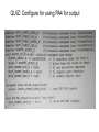
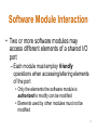
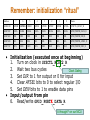
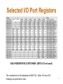
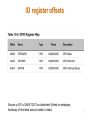
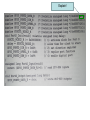
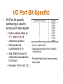
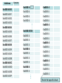
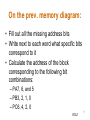
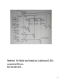
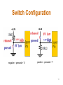
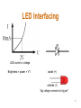
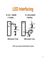
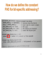
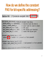
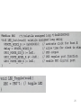
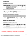
Discussion of exam problems and scores 1 QUIZ: Configure for using PA4 for output Text sections 4.2.1 Bit-specific addressing 4.2.2 Switches and LEDs 3 Software Module Interaction • Two or more software modules may access different elements of a shared I/O port – Each module must employ friendly operations when accessing/altering elements of the port • Only the elements the software module is authorized to modify can be modified • Elements used by other modules must not be modified 4 Remember: initialization “ritual” Address 7 6 5 4 3 2 1 0 Name 400F.E108 GPIOH GPIOG GPIOF GPIOE GPIOD GPIOC GPIOB GPIOA SYSCTL_RCGC2_R 4000.73FC DATA DATA DATA DATA DATA DATA DATA DATA GPIO_PORTD_DATA_R 4000.7400 DIR DIR DIR DIR DIR DIR DIR DIR GPIO_PORTD_DIR_R 4000.7420 SEL SEL SEL SEL SEL SEL SEL SEL GPIO_PORTD_AFSEL_R 4000.751C DEN DEN DEN DEN DEN DEN DEN DEN GPIO_PORTD_DEN_R • Initialization (executed once at beginning) 1. Turn on clock in SYSCTL_RCGC2_R 2. Wait two bus cycles Clock Gating 3. Set DIR to 1 for output or 0 for input 4. Clear AFSEL bits to 0 to select regular I/O 5. Set DEN bits to 1 to enable data pins • Input/output from pin 6. Read/write GPIO_PORTX_DATA_R A through F on our MCU Selected I/O Port Registers EACH REGISTER IS 32 BITS WIDE (BITS 8-31 not used) The complete list is in the datasheet of LM4F120 – Table 10-6 on p.632. Hardcopy was provided in class. 6 IO register offsets Source: p.631 of LM4F120-Tiva datasheet (linked on webpage, hardcopy of this table was provided in class) 7 Explain! I/O Port Bit-Specific • I/O Port bit-specific addressing is used to access port data register – Define address offset as 4*2b, where b is the selected bit position – 256 possible bit combinations (0-8) – Add offsets for each bit selected to base address for the port – Example: Port A, bits 1,2,3 Port A = 0x4000.4000 0x4000.4000+0x0008+0x0010+0x0020 = 0x4000.4038 Provides friendly and atomic access to port pins 9 Address 0x4000 4000 0x4000 4001 0x4000 4002 0x4000 4003 Contents 0x4000 4 0x4000 4 0x4000 4 0x4000 4 0x4000 4 0x4000 4 0x4000 4 0x4000 4 0x4000 4 0x4000 4004 0x4000 4005 0x4000 41D8 0x4000 4006 0x4000 4 0x4000 4007 0x4000 4 0x4000 4008 0x4000 4 0x4000 4009 0x4000 4 0x4000 400A 0x4000 4 0x4000 400B 0x4000 4 0x4000 400C 0x4000 4 0x4000 400D 0x4000 4 0x4000 400E 0x4000 4 0x4000 400F 0x4000 4 0x4000 4 0x4000 4 0x4000 4 0x4000 4 0x4000 4 0x4000 4 0x4000 4 0x4000 4 0x4000 4 0x4000 4 End of bit-specific block On the prev. memory diagram: • Fill out all the missing address bits • Write next to each word what specific bits correspond to it • Calculate the address of the block corresponding to the following bit combinations: – PA7, 6, and 5 – PB3, 2, 1, 0 – PC6, 4, 2, 0 EOL1 11 Remember: The Stellaris board already has 2 switches and 3 LEDs connected to MCU pins. But if we need more … 12 Switch Configuration negative – pressed = ‘0’ positive – pressed = ‘1’ 13 LED Interfacing LED current v. voltage Brightness = power = V*I anode (+) cathode (1) “big voltage connects to big pin” 14 LED Interfacing R = (3V – 1.5)/0.001 = 1.5 kOhm PE0 LM3S R = (5.0-2-0.5)/0.01 = 220 Ohm +5V high R LM3S R 1mA +5V LED PE0 high 10mA LED 0.5V 7405 LED current < 8 ma LED current > 8 ma LED may contain several diodes in series 15 How do we define the constant PA5 for bit-specific addressing? 16 How do we define the constant PA5 for bit-specific addressing? 17 Make PA7 output, the set, clear and toggle (use both methods!) 18 Your turn: Configure PB7 and PB5 for output … … then set set 7 and clear 5 (use both methods!) 19 Example 4.1: Generating out-of-phase square waves on PG1 and PG0 Modify the code to use port E instead! 20 21 To do for next time: Read and understand the remaining examples in 4.2.2 22 QUIZ: Bit-specific addressing Fill in the missing parts of the”ritual” 23 QUIZ: Bit-specific addressing 24 QUIZ: Bit-specific addressing Write in C a function that toggles the LED connected to pin PE0 25 26 4.3 PLL • LM4F120 has 16 MHz crystal • Remember “CV2F” power fmla. for CMOS! • A CMOS circuit operates with VDD = 3.3V. What is the power savings if VDD is reduced to 2.5V? 27 4.3 PLL • LM4F120 has 16 MHz crystal • Remember “CV2F” power fmla. for CMOS! • A CMOS circuit operates with f = 40 MHz. What is the power savings if: – f is reduced to 20 MHz? – f is increased to 80 MHz? 28 What is the power savings when LM4F120 hibernates? 29 Source: Tiva™ TM4C1233H6PM Microcontroller (identical to LM4F120H5QR) DATA SHEET Real Time Clock (see next slide) 30 Source: Tiva™ TM4C1233H6PM Microcontroller (identical to LM4F120H5QR) DATA SHEET, p.52 FYI 31 Source: Tiva™ TM4C1233H6PM Microcontroller (identical to LM4F120H5QR) DATA SHEET FYI: Our board comes with both crystals: MOSC (Y2) and hibernation module (Y1) 32 Source: Stellaris® LM4F120 LaunchPad Evaluation Board User Manual PLL MOSC OSCSRC External crystal Main Osc BYPASS 00 USESYSDIV Mux 01 12 MHz Internal Osc /4 10 1 Ref Clk Phase-Lock-Loop Up Phase/ Charge Freq Down Pump/ Detector LPF /m PIOSC VCO 200 MHz Mux 0 0 Mux /n 1 Bus (a.k.a. “core”) clock SYSDIV XTAL Internal oscillator requires minimal power but is imprecise External crystal provides stable bus clock LM4F120 is equipped with a 16 MHz crystal, and the bus clock is typically set at 50 MHz 33 FYI External 16 MHz External 16 MHz Source: Tiva™ TM4C1233H6PM Microcontroller (identical to LM4F120H5QR) DATA SHEET 35 Source: Tiva™ TM4C1233H6PM Microcontroller (identical to LM4F120H5QR) DATA SHEET 36 Source: Tiva™ TM4C1233H6PM Microcontroller (identical to LM4F120H5QR) DATA SHEET Your turn! Using the 16 MHz CLK as the source, how should we set the multiplier to obtain: • A 50 MHz clock? • A reduction in power by 75%? EOL2 37 QUIZ: Bit-specific addressing 38 Designing a complete Hw-Sw system: SSR = Solid-State Relay What is there to design? PN2222 specs: • max. ICE = 150 mA • VCE = 0.3V 39 Designing a complete Hw-Sw system: SSR = Solid-State Relay PN2222 specs: • max. ICE = 150 mA • VCE = 0.3V 40 Designing a complete Hw-Sw system: 41 QUIZ: Bit-specific addressing Fill in the missing parts of the”ritual” 42 Write C functions that turn the SSR on and off, using toggle as template! 43 4.4 SysTick Timer Timer/Counter operation • 24-bit counter decrements at bus clock frequency – With 50 MHz bus clock, decrements occur every 20 ns • Counting is from n 0 – For a count of m, (m-1) is loaded into the counter 44 SysTick Timer Initialization – – – – Address $E000E010 $E000E014 $E000E018 Clear ENABLE to stop counter Specify the RELOAD value Clear the counter via NVIC_ST_CURRENT_R Set CLK-SRC=1 and specify interrupt action via INTEN in NVIC_ST_CTRL_R 31-24 0 0 0 23-17 0 16 COUNT 15-3 2 1 0 0 CLK_SRC INTEN ENABLE 24-bit RELOAD value 24-bit CURRENT value of SysTick counter Name NVIC_ST_CTRL_R NVIC_ST_RELOAD_R NVIC_ST_CURRENT_R 45 Address $E000E010 $E000E014 $E000E018 31-24 0 0 0 23-17 0 16 COUNT 15-3 2 1 0 0 CLK_SRC INTEN ENABLE 24-bit RELOAD value 24-bit CURRENT value of SysTick counter Name NVIC_ST_CTRL_R NVIC_ST_RELOAD_R NVIC_ST_CURRENT_R 46 Why do we need this? A: To account for possible counter rollover! Address $E000E010 $E000E014 $E000E018 31-24 0 0 0 23-17 0 16 COUNT 15-3 2 1 0 0 CLK_SRC INTEN ENABLE 24-bit RELOAD value 24-bit CURRENT value of SysTick counter Name NVIC_ST_CTRL_R NVIC_ST_RELOAD_R NVIC_ST_CURRENT_R 47 SKIP 4.5 OLED READ 4.6 Debugging monitor using LED 48 4.6 Debugging monitor using LED How many bus cycles does this code take to execute? 49 4.7 Performance Debugging Using SysTick to time a segment of code 50 Homework for Ch.4 • End of chapter 6, 7, 10, 12, 13, 17 • Due Thu, Nov.7 51