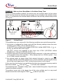
1
Errata Sheet
V1.1, 2005-07-05
Device
C164CM-4EF
Marking/Step
Step (E)ES-AB, AB
Package
P-TQFP-64
This Errata Sheet describes the deviations from the current user documentation.
The module oriented classification and numbering system uses an ascending sequence
over several derivatives, including already solved deviations. So gaps inside this
enumeration can occur.
Current Documentation
• C164CM/SM Data Sheet, V1.0, May 2001
• C164CM/SM User’s Manual, V1.0, Feb. 2002
• Instruction Set Manual, V2.0, Mar. 2001
Note: Devices marked with EES- or ES are engineering samples which may not be
completely tested in all functional and electrical characteristics, therefore they
should be used for evaluation only. The specific test conditions for EES and ES
are documented in a separate Status Sheet.
Note: For simplicity all versions are referred to by the term C164CM-4EF throughout this
document.
Contents
Section . . . . . . . . . . . . . . . . . . . . . . . . . . . . . . . . . . . . . . . . . . . . . . . . . . . . . . . . . . Page
History List/Change Summary . . . . . . . . . . . . . . . . . . . . . . . . . . . . . . . . . . . . . . . . . .2
Functional Problems . . . . . . . . . . . . . . . . . . . . . . . . . . . . . . . . . . . . . . . . . . . . . . . . . .4
Deviations from Electrical- and Timing Specification. . . . . . . . . . . . . . . . . . . . . . .19
Application Hints . . . . . . . . . . . . . . . . . . . . . . . . . . . . . . . . . . . . . . . . . . . . . . . . . . . .20
Documentation Update . . . . . . . . . . . . . . . . . . . . . . . . . . . . . . . . . . . . . . . . . . . . . . .25
C164CM-4EF, Step (E)ES-AB, AB
1/27
es, V1.1, 2005-07-05
Errata Sheet
History List/Change Summary
1
History List/Change Summary
(from step AA, previous errata sheet V1.0, step: AB)
Table 1
Functional Deviations
Functional
Problem
Short Description
ADC.11
Modifications of ADM field while bit ADST = 0
SSC.9
Data Transmission in Slave Mode
CAN.7
Unexpected Remote Frame Transmission
CAN.9
Contents of Message Objects and Mask of Last
Message Registers after Reset
Fixed Change
in step
CAPCOM6.4 Spike when enabling alternate Port Function
X9
Read Access to XPERs in Visible Mode
OTP.8
Programming Voltage VPP and Supply Voltage VDD
CPU.22
Z Flag after PUSH and PCALL
PLL.3.6
Increased PLL Jitter caused by external Access
PWRDN.1
Execution of PWRDN instruction while Pin
NMI = high
POWER.20.2
Wake up from Sleep Mode not possible with fast
external interrupt (name changed from POWER.20)
POWER.22
Wake up from Sleep Mode in Oscillator Decay Time
RST.13.1
Power Up with missing clock
(name changed from RST.13)
ADCC.2.9
ADC Overload Current
Table 2
AC/DC Deviations
AC/DC
Deviations
Short Description
AA
new
AA
Fixed
Change
in step
no deviations found
C164CM-4EF, Step (E)ES-AB, AB
2/27
es, V1.1, 2005-07-05
Errata Sheet
History List/Change Summary
Table 3
Application Hints
Hint
Short Description
SSC.H1
Handling of the SSC Busy Flag (SSCBSY)
SSC.H2
Timing of flag SSCTIR (SSC Transmit Interrupt Request)
CAN.H1
Note on Interrupt Register behaviour of the CAN module
EMUL.H1
Adapt Mode Setting
OTP.H1
OTP Read access in CHM Mode delivers Zeros only
BSL.H1
Bootstrap Loader: Baudrate Detection in Single Chip Boot
Mode
Change
MainOsc.H1 Oscillator Type_LP2: Negative Resistance and Start-up
Reliability
MainOsc.H2 Maximum (Type_LP2) Oscillator Frequency = 16 MHz
OWD.H2
Oscillator Watchdog and Prescaler Mode
ISNC.H1
Maintenance of ISNC Register
Table 4
Documentation Update
Name
Short Description
Change
INT.D2
CCxIC Registers
PLL.D1
PLL goes to Unlocked State after Configuration
PACKAGE.D1 P-TQFP64-8 Package used
VIH.D1
Input High Voltage at Pin EA
ID-Registers
ID-Registers
C164CM-4EF, Step (E)ES-AB, AB
3/27
es, V1.1, 2005-07-05
Errata Sheet
Functional Problems
2
Functional Problems
ADC.11 Modifications of ADM field while bit ADST = 0
The A/D converter may unintentionally start one auto scan single conversion sequence
when the following sequence of conditions is true:
1. the A/D converter has finished a fixed channel single conversion of an analog channel
n > 0 (i.e. contents of ADCH (ADCON.3-0) = n during this conversion)
2. the A/D converter is idle (i.e. ADBSY (ADCON.8) = 0)
3. then the conversion mode in the ADC Mode Selection field ADM (ADCON.5-4) is
changed to Auto Scan Single (ADM = 10B) or Continuous (ADM = 11B) mode without
setting bit ADST = 1 with the same instruction
Under these conditions, the A/D converter will unintentionally start one auto scan single
conversion sequence, beginning with channel n-1, down to channel number 0.
When no interrupt or PEC is servicing the A/D Conversion Complete Interrupt, interrupt
request flag ADCIR (ADCIC.7) will be set, and for n > 1 also the A/D Overrun Error
interrupt request flag will be set, unless the wait for ADDAT read mode had been
selected. When ADWR (ADCON.9) = 1 (wait for ADDAT read), the converter will wait
after 2 conversions until ADDAT is read.
In case the channel number ADCH has been changed before or with the same
instruction which selected the auto scan mode, this channel number has no effect on the
unintended auto scan sequence (i.e. it is not used in this auto scan sequence).
Note:
When a conversion is already in progress, and then the configuration in register ADCON
is changed,
• the new conversion mode in ADM is evaluated after the current conversion
• the new channel number in ADCH and new status of bit ADST are evaluated after the
current conversion when a conversion in fixed channel conversion mode is in
progress, and after the current conversion sequence (i.e. after conversion of
channel 0) when a conversion in an auto scan mode is in progress.
In this case, it is a specified operational behaviour that channels n-1 .. 0 are converted
when ADM is changed to an auto scan mode while a fixed channel conversion of
channel n is in progress (see e.g. C164CI User's Manual, V1.0, p.18-4)
Workaround:
When an auto scan conversion is to be performed, always start the A/D converter with
the same instruction which sets the configuration in register ADCON.
C164CM-4EF, Step (E)ES-AB, AB
4/27
es, V1.1, 2005-07-05
Errata Sheet
Functional Problems
SSC.9 Data Transmission in Slave Mode
During data reception in slave mode of the SSC module, sporadically the shift clock
supplied by the external master on pin SCLK may not be properly recognized due to a
synchronization problem when all of the following conditions are true:
1. the latching edge for the serial data is the falling edge of SCLK (i.e. both bit
SSCPO = 1 and bit SSCPH = 1, or SSCPO = 0 and SSCPH = 0 in register SSCCON),
and
2. the transmit buffer SSCTB of the slave has not been written prior to the start of the
reception (initiated by the master asserting the shift clock SCLK), and
3. a specific time window (phase delay) is hit by the serial shift clock SCLK in relation to
the internal system clock of the slave. Therefore, this synchronization problem will
occur in particular when the slave device is clocked (on XTAL1) by an external clock
generation circuit which is independent from the clock generation circuit of the master
(i.e. slave and master clocks are asynchronous).
When the problem occurs, this results in missing bits in the character received in
SSCTB, and in duplicated bits in the character transmitted on pin MRST of the slave. As
a consequence, interrupt generation in the slave is delayed by the number of missed
bits.
Workaround
For systems using the falling edge of SCLK as latching edge (see condition 1. above),
always write to the transmit buffer SSCTB prior to any reception in slave mode of the
SSC module. For the second and all following characters, e.g. write a (dummy) character
to SSCTB in the receive interrupt routine, or use a PEC transfer triggered by the transmit
interrupt request to write to SSCTB. In this case, the critical synchronization path is not
used, and the problem will not occur.
CAN.7 Unexpected Remote Frame Transmission
Symptom:
The on-chip CAN module may send an unexpected remote frame with the identifier = 0,
when a pending transmit request of a message object is disabled by software.
Detailed Description:
There are three possibilities to disable a pending transmit request of a message object
(n = 1..14):
• Set CPUUPDn element
• Reset TXRQn element
C164CM-4EF, Step (E)ES-AB, AB
5/27
es, V1.1, 2005-07-05
Errata Sheet
Functional Problems
• Reset MSGVALn element
Either of these actions will prevent further transmissions of message object n.
The symptom described above occurs when the CPU accesses CPUUPD, TXRQ or
MSGVAL, while the pending transmit request of the corresponding message object is
transferred to the CAN state machine (just before start of frame transmission). At this
particular time the transmit request is transferred to the CAN state machine before the
CPU prevents transmission. In this case the transmit request is still accepted from the
CAN state machine. However the transfer of the identifier, the data length code and the
data of the corresponding message object is prevented. Then the pre-charge values of
the internal "hidden buffer" are transmitted instead, this causes to a remote frame
transmission with identifier = 0 (11 bit) and data length code = 0.
This behavior occurs only when the transmit request of message object n is pending and
the transmit requests of other message objects are not active (single transmit request).
If this remote frame loses arbitration (to a data frame with identifier = 0) or if it is disturbed
by an error frame, it is not retransmitted.
Effects to other CAN nodes in the network:
The effect leads to delays of other pending messages in the CAN network due to the high
priority of the Remote Frame. Furthermore the unexpected remote frame can trigger
other data frames depending on the CAN node's configuration.
Workarounds:
• The behavior can be avoided if a message object is not updated by software when a
transmission of the corresponding message object is pending (TXRQ element is set)
and the CAN module is active (INIT = 0). If a re-transmission of a message (e.g. after
lost arbitration or after the occurrence of an error frame) needs to be cancelled, the
TXRQ element should be cleared by software as soon as NEWDAT is reset from the
CAN module.
• The nodes in the CAN system ignore the remote frame with the identifier = 0 and no
data frame is triggered by this remote frame.
CAN.9 Contents of Message Objects and Mask of Last Message Registers after
Reset
After any reset, the contents of the CAN Message Objects and the Mask of Last
Message Registers may be undefined instead of unaffected (reset value 'X' instead
of 'U').
C164CM-4EF, Step (E)ES-AB, AB
6/27
es, V1.1, 2005-07-05
Errata Sheet
Functional Problems
This problem depends on temperature and the length of the reset, and differs from
device to device. The problem is more likely to occur at high temperature and for long
hardware resets (> 100 ms).
Workaround:
Re-initialize the CAN module after each reset.
CAPCOM6.4 Spike when enabling alternate Port Function
When switching a port from I/O mode to compare mode during the low state of the PWM
by setting bits in register CC6MSEL, a spike is generated for one TCL before the PMW
signal starts.
Workaround:
When the port configuration is changed during the high phase of the compare output the
spike is suppressed. Two different interrupts can be used for this synchronization
depending on the initial value bits in the register CC6MCON (CCxI and COUTxI
represent the passive output level for the enabled compare channels). The first high
phase of the PWM signal is delayed by the corresponding interrupt latency and the
execution time of the necessary instructions:
• If the initial value is 0, the compare interrupt service routine switches the port to
compare output. So the spike is pushed in the high phase of the PWM.
• If the initial value is 1, the Timer 12 period match interrupt service routine switches the
port to compare mode with the same result.
X9 Read Access to XPERs in Visible Mode
The data of a read access to an XBUS-Peripheral (CAN) in Visible Mode
(SYSCON.1 = 1) is not driven to the external bus. PORT0 is tristated during such read
accesses.
Note that in Visible Mode PORT1 will drive the address for an access to an XBUSPeripheral, even when only a multiplexed external bus is enabled.
OTP.8 Programming Voltage VPP and Supply Voltage VDD
To guarantee a proper internal OTP programming the tolerances for supply voltage VDD
and programming voltage VPP are reduced.
C164CM-4EF, Step (E)ES-AB, AB
7/27
es, V1.1, 2005-07-05
Errata Sheet
Functional Problems
The following values have been successfully tested and can be recommended:
Supply Voltage VDD
Programming Voltage VPP
4.35V - 4.65V
11.35V - 11.65V
4.85V - 5.15V
11.8V - 12.1V
Application Hints:
• Devices formerly programmed with these recommended values can be used without
restriction.
• Software for OTP programming tools should be adapted to one of these recommended values
(VDD = 4.85V - 5.15V and VPP = 11.8 - 12.1V can still be used after the problem is
fixed in the future).
CPU.22 Z Flag after PUSH and PCALL
The Z flag in the PSW is erroneously set to '1' by PUSH reg or PCALL reg, rel
instructions when all of the following conditions are true:
a) for PUSH reg instructions:
• the contents of the high byte of the GPR or (E)SFR which is pushed is 00H, and
• the contents of the low byte of the GPR or (E)SFR which is pushed is > 00H, and
• the contents of GPR Rx is odd, where x = 4 msbs of the 8-bit 'reg' address of the
pushed GPR or (E)SFR
Examples:
PUSH
PUSH
R1
;(coding: F1
; incorrect
; and 00FFh
DPP3 ;(coding: 03
; incorrect
; and 00FFh
EC):
setting of
≥ contents
EC):
setting of
≥ contents
Z flag if contents of R15 is odd,
of R1 ≥ 0001h
Z flag if contents of R0 is odd,
of DPP3 ≥ 0001h
b) for PCALL reg, rel instructions:
• when the contents of the high byte of the GPR or SFR which is pushed is 00H, and
• when the contents of the low byte of the GPR or SFR which is pushed is odd
C164CM-4EF, Step (E)ES-AB, AB
8/27
es, V1.1, 2005-07-05
Errata Sheet
Functional Problems
This may lead to wrong results of instructions following PUSH or PCALL if those
instructions explicitly (e.g. BMOV .. , Z; JB Z, ..; ..) or implicitly (e.g. JMP cc_Z, ..; JMP
cc_NET, ..; ..) evaluate the status of the Z flag before it is newly updated.
Note: Some instructions (e.g. CALL, ..) have no effect on the status flags, such that the
status of the Z flag remains incorrect after a PUSH/PCALL instruction until an
instruction that correctly updates the Z flag is executed.
Example:
PUSH
R1
CALL
proc_xyz
...
...
proc_xyz:
JMP
cc_Z,end_xyz
...
end_xyz:
; incorrect setting of Z flag if R15 is odd
; Z flag remains unchanged
; (is a parameter for proc_xyz)
; Z flag evaluated with incorrect setting
Effect on Tools:
• The Hightec C166 tools (all versions) don't use the combination of PUSH/PCALL and
the evaluation of the Z flag. Therefore, these tools are not affected.
• The code generated by the Keil C166 Compiler evaluates the Z flag only after MOV,
CMP, arithmetic, or logical instructions. It is never evaluated after a PUSH instruction.
PCALL instructions are not generated by the C166 Compiler.
This has been checked with all C166 V3.xx and V4.xx compiler versions. Even the
upcoming V5.xx is not affected by the CPU.22 problem.
The assembler portions of the C166 V3.xx and V4.xx Run-Time Libraries, the RTX166
Full and TX166 Tiny Real Time Operating system do also not contain any evaluation
of the Z flag after PUSH or PCALL.
• The TASKING compiler V7.5r2 never generates a PCALL instruction, nor is it used in
the libraries.
The PUSH instruction is only used in the entry of an interrupt frame, and sometimes
on exit of normal functions. The zero flag is not a parameter or return value, so this
does not give any problems.
Previous versions of TASKING tools:
C164CM-4EF, Step (E)ES-AB, AB
9/27
es, V1.1, 2005-07-05
Errata Sheet
Functional Problems
V3.x and higher are not affected, versions before 3.x are most likely not affected.
Contact TASKING when using versions before V3.x.
Since code generated by the C166 compiler versions mentioned before is not
affected, analysis and workarounds are only required for program parts written in
assembler, or instruction sequences inserted via inline assembly.
Workaround (for program parts written in assembler):
Do not evaluate the status of the Z flag generated by a PUSH or PCALL instruction.
Instead, insert an instruction that correctly updates the PSW flags, e.g.
PUSH
CMP
JMPR
reg
reg, #0
; note:
; CMP additionally modifies the C and V flags,
; while PUSH or MOV leaves them unaffected
cc_Z, label_1; implicitly tests Z flag
or
PCALL reg, procedure_1
...
procedure_1:
MOV
ONES, reg
JMPR
cc_NET, label_1 ; implicitly tests flags Z and E
Hints for Detection of Critical Instruction Combinations
Whether or not an instruction following PUSH reg or PCALL reg, rel actually causes a
problem depends on the program context.
In most cases, it will be sufficient to just analyze the instruction following PUSH or
PCALL. In case of PCALL, this is the instruction at the call target address.
Support Tool for Analysis of Hex Files
For complex software projects, where a large number of assembler source (or list) files
would have to be analyzed, Infineon provides a tool aiScan22 which scans hex files for
critical instruction sequences and outputs diagnostic information. This tool is available
as part of the Application Note ap1679 'Scanning for Problem CPU.22' on the 16-bit
microcontroller internet pages of Infineon Technologies:
www.infineon.com/16-bit-microcontrollers
direct links:
AP1679 Description: www.infineon.com/cmc_upload/documents/040/841/
C164CM-4EF, Step (E)ES-AB, AB
10/27
es, V1.1, 2005-07-05
Errata Sheet
Functional Problems
ap1679_v1.1_2002_05_scanning_cpu22.pdf and
AP1679 Software: www.infineon.com/cgi/ecrm.dll/ecrm/scripts/
public_download.jsp?oid=40840&parent_oid=-8984
Individual Analysis of Assembler Source Code
With respect to problem CPU.22, all instructions of the C166 instruction set can be
classified into the following groups:
• Arithmetic/logic/data movement instructions as successors of PUSH/PCALL
(correctly) modify the condition flags in the PSW according to the result of the
operation.
These instructions may only cause a problem if the PSW is a source or source/
destination operand:
ADD/B, ADDC/B, CMP/B, CMPD1/2, CMPI1/2, SUB/B, SUBC/B
AND/B, OR/B, XOR/B
ASHR
MOV/B, MOVBZ/MOVBS
SCXT
PUSH, PCALL Î analysis must be repeated for successor of PUSH/PCALL
• The following instructions (most of them with immediate or register (Rx) addressing
modes) can never cause a problem:
CPL/B, NEG/B
DIV/U, DIVL/U, MUL/U
SHL/SHR, ROL/ROR
PRIOR
POP
RETI
Î updates complete PSW with stacked value
RETP
Î updates condition flags
PWRDN Î program restarts after reset
SRST
Î program restarts
• Conditional branch instructions which may evaluate the Z flag:
JB/JNB Z, rel ; directly evaluates Z flag
CALLA/CALLI, JMPA/JMPI/JMPR with the following condition codes
cc_Z, cc_EQ, cc_NZ, cc_NE
cc_ULE, cc_UGT, cc_SLE, cc_SGT
cc_NET
Î For these branch conditions, the branch may be performed in the wrong way.
Î For other branch conditions, the branch target as well as the linear successor of
the branch instruction must be analyzed (since these branch instruction don't modify
C164CM-4EF, Step (E)ES-AB, AB
11/27
es, V1.1, 2005-07-05
Errata Sheet
Functional Problems
the PSW flags).
• For instructions that have no effect on the condition flags and that don't evaluate
the Z flag, the instruction that follows this instruction must be analyzed.
These instructions are:
NOP
ATOMIC, EXTxx
DISWDT, EINIT, IDLE, SRVWDT
CALLR, CALLS, JMPS
Î branch target must be analyzed
RET, RETS Î return target must be analyzed
(value pushed by PUSH/PCALL = return IP, Z flag contains
information whether intra-segment target address = 0000H or not)
TRAP Î both trap target and linear successor must be analyzed, since Z flag may
be incorrect in PSW on stack as well as in PSW at entry of trap routine
• For bit modification instructions, the problem may only occur if a source bit is the
Z flag, and/or the destination bit is in the PSW, but not the Z flag.
These instructions are:
BMOV/BMOVN
BAND/BOR/BXOR
BCMP
BFLDH
BFLDL
Î problem only if bit 3 of @@ mask = 0, i.e. if Z is not selected
BCLR/BSET Î problem only if operand is not Z flag
JBC/JNBS Î wrong branch if operand is Z flag
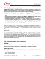
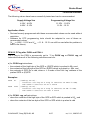
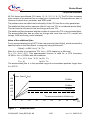
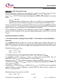
PLL.3.6 Increased PLL Jitter caused by external Access
Problem description:
In systems were the PLL is used for generation of the CPU clock frequency, the PLL jitter
can increase in certain circumstances and exceed the specified value.
The value of the additional jitter is not a fixed one but it depends on the kind of activity
on the external bus or output pins. The additional jitter increases with the number of
output/bus pins which are switched at the same time to a new voltage level because the
problem is caused by noise on the on-chip power supply.
The capacitive load of the used pins has also an influence to the additional jitter. A high
capacitive load can increase the additional jitter.
Effects to the system:
C164CM-4EF, Step (E)ES-AB, AB
12/27
es, V1.1, 2005-07-05
Errata Sheet
Functional Problems
All PLL factors are affected (PLL factor 1,5 / 2 / 2,5 / 3 / 4 / 5). The PLL jitter increases
when access to the external bus or output pins is performed. This phenomenon has no
influence to direct drive- prescaler- and SDD mode.
The problem does not affect the functionality of the CPU and the on-chip peripherals.
The additional jitter has the maximum effect if only one TCL is considered (period jitter).
This can have an influence to the bus timings with one TCL.
The additional jitter decreases with the number of consecutive TCLs (accumulated jitter).
The accumulated jitter has an effect on timings with more than one TCL (certain bus
timings, CAN bus timing, serial interface).
Value of the additional jitter:
For an accumulated period of N*TCL the new maximum jitter DN[ns], which exceeds the
specified value in the Data Sheet, is computed using the formula:
DN[ns] = ±(266 / fCPU) * N / Tm
Were N = number of consecutive TCL, fCPU = CPU frequency in MHz and
Tm = 11.3 - fCPU * 0.13. This approximated formula is valid for a CPU frequency
10 MHz ≤ fCPU ≤ 20 MHz with the conditions:
Tm = 11.3 - fCPU * 0.13 for N ≤ Tm
Tm = N
for N > Tm
The accumulated jitter is in the specified range for accumulated periodes longer than
N = 40 TCL.
±30
max. Jitter DN[ns]
10 MHz
±25
±20
16 MHz
±15
20 MHz
±10
25 MHz *)
±5
0
*)
1
Figure 1
5
10
15
20
for devices specified for 25 MHz only
25
30
35
40
TCL
Additional Jitter
C164CM-4EF, Step (E)ES-AB, AB
13/27
es, V1.1, 2005-07-05
Errata Sheet
Functional Problems
Workaround:
In the case that the additional jitter causes problems in the system which cannot be
relaxed with software adapted timing parameters the following workarounds are
possible:
• If the clock generation is done with the on-chip oscillator then direct drive- or prescaler
mode can be used.
• If the maximum frequency of the on-chip oscillator in not sufficient then an external
clock generator can be used.
PWRDN.1 Execution of PWRDN Instruction while pin NMI = high
When instruction PWRDN is executed while pin NMI is at a high level, power down mode
should not be entered, and the PWRDN instruction should be ignored. However, under
the conditions described below, the PWRDN instruction may not be ignored, and no
further instructions are fetched from external memory, i.e. the CPU is in a quasi-idle
state. This problem will only occur in the following situations:
a) the instructions following the PWRDN instruction are located in external memory, and
a multiplexed bus configuration with memory tristate waitstate (bit MTTCx = 0) is used, or
b) the instruction preceeding the PWRDN instruction writes to external memory or an
XPeripheral (e.g. CAN or XRAM), and the instructions following the PWRDN instruction
are located in external memory. In this case, the problem will occur for any bus
configuration.
Note: The on-chip peripherals are still working correctly, in particular the Watchdog
Timer will reset the device upon an overflow. Interrupts and PEC transfers,
however, can not be processed. In case NMI is asserted low while the device is in
this quasi-idle state, power down mode is entered.
Workaround:
Ensure that no instruction which writes to external memory or an XPeripheral preceeds
the PWRDN instruction, otherwise insert e.g. a NOP instruction in front of PWRDN.
When a muliplexed bus with memory tristate waitstate is used, the PWRDN instruction
should be executed out of internal RAM.
C164CM-4EF, Step (E)ES-AB, AB
14/27
es, V1.1, 2005-07-05
Errata Sheet
Functional Problems
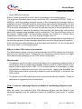
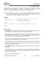
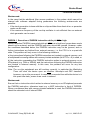
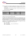
POWER.22 Wake up from Sleep Mode in Oscillator Decay Time
cyclic wake up from
sleep mode
wa
ke
sle
up
ep
mo
de
mode
VIH threshold
VIL threshold
tCRIT
Entry into sleep mode
Figure 2
om
ran
d
sleep
tOSC
fro
m
random
tDECAY
random
wake u
p
from s
leep m
ode
wake u
p
fr om sl
eep mo
de
Due to a synchronization problem, the device may not correctly wake up from sleep
mode if an asynchronous external wake up trigger occurs already in the oscillator decay
time, i.e. in a particular time window before the device has actually entered sleep mode
(see figure)
Critical Event
This problem may occur when all of the following conditions are met at the same time:
1. the device is configured for sleep mode with the following settings where the main
oscillator (input XTAL1) will be switched off, i.e.
a) with RTC and oscillator to be stopped (SYSCON1 bitfield SLEEPCON = 11B), or
b) only for devices with XTAL3 input:
with RTC running and supplied by the clock from XTAL3 (SYSCON1 bitfield
SLEEPCON = 01B and SYSCON2 bit RCS = 1)
2. the IDLE instruction to enter sleep mode has been executed, i.e. the main oscillator is
in the oscillator decay time (typically ~ 160 µs decay time for a 16 MHz crystal, ~ 2 µs
for a 16 MHz ceramic resonator)
3. the external wake up trigger signal (fast external interrupt or signal on pin NMI)
coincides with the critical time window (tCRIT) of each oscillator cycle during the decay
time of the clock signal at pin XTAL1 (critical times shown in red in figure)
In this case the clock system may get blocked but the internal program memory module
becomes enabled. IDDI rises up to IPDR ... 3 mA with main oscillator.
The watchdog timer - stopped in sleep mode - cannot restart the system. Only HW reset
restarts the system properly.
The problem occurs only in the decay time of the main oscillator and in a very small
window around the clock edge at XTAL1 (tCRIT is about 5 ps wide).
C164CM-4EF, Step (E)ES-AB, AB
15/27
es, V1.1, 2005-07-05
Errata Sheet
Functional Problems
The following formula shows a risk calculation for an asynchronous (random) wake up
event at any time within a 100 ms sleep period (16 MHz crystal/resonator):
PLock-Up = PSensitive Device* PCritical Wake-Up-Event
PLock-Up = 5 ps (critical window) / 62500 ps (one 16 MHz oscillator period)
* 160 µs (typical crystal decay time) / 100000 µs (wake up after 100 ms)
PLock-Up = 5 / 62500 * 160 / 100000 = 0.000'000'13
= 0.13 failure events per 1 million random wake up events (for a 16 MHz crystal)
The decay time of a resonator circuit is below 2 µs typically:
PLock-Up (resonator) = 5 / 62500 * 2 / 100000 = 0.000'000'001’6
= 0.0016 failure events per 1 million random wake up events
(for a 16 MHz resonator)
Note: A cyclic wake up event would never cause the problem as it happens well after
entry into sleep mode and after the decay time.
Workarounds:
• Select RTC on in sleep mode (SYSCON1.SLEEPCON = 01B).
For devices with auxiliary oscillator (e.g. C161CS), select main oscillator as clock
source (SYSCON2.RCS = 0).
• Avoid a wake up during the main oscillator decay time
C164CM-4EF, Step (E)ES-AB, AB
16/27
es, V1.1, 2005-07-05
Errata Sheet
Functional Problems
ADCC.2.9 ADC Overload Current
During exceptional conditions in the application system an overload current IOV can
occur on the analog inputs of the A/D converter when VAIN > VDD + 0.5 V or
VAIN < VSS - 0.5 V. For this case, the following conditions are specified in the Data
Sheet:
IOVmax = | ±5 mA |
The specified total unadjusted error TUEmax = | ±2 LSB | is only guaranteed if the
absolute sum of input overload currents on Port5 pins does not exceed 10 mA.
Due to an internal problem, the specified TUE value is only met for a positive overload
current 0 mA ≤ IOV ≤ +5 mA (all currents flowing into the microcontroller are defined as
positive and all currents flowing out of it are defined as negative).
If the exceptional conditions in the application system cause a negative overload
current, then the maximum TUE can be exceeded (depending on value of IOV, RAIN and
RAREF):
Problem Description in Detail:
1. Overload Current at Analog Channel AN(0 - 7) and Influence to the Neighbour
Channels
If a negative overload current IOV occurs on analog input channel ANn then an
additional current IAN (crosstalk current) is caused at the neighbour channels ANn-1 and
ANn+1. This behavior can cause an additional unadjusted error AUE to the ADC result.
Relation between IAN and IOV:
IANn+1 = ovf-1 * IOVn
IANn-1 = ovf-1 * IOVn
1.1 Overload Current at Analog Channel AN0 and Influence to VAREF
If a negative overload current IOV occurs on analog input channel AN0
additional current IAREF (crosstalk current) is caused at pin VAREF.
then an
Depending on RAREF, the resistance between voltage reference and input VAREF, the
crosstalk current IAREF at pin VAREF can cause an additional unadjusted error AUE to all
other analog channels.
In case RAREF ≤ 975 Ohm [RAREF ≤ ((LSB10/2) / (|IOVmax| * ovf-3)] the maximum possible
additional error to all other channels is smaller than 0.5 LSB10 with the condition of
IOVmax = |-5 mA| at AN0.
Relation between IAREF and IOV at AN0:
IAREF = ovf-3 * IOVn
C164CM-4EF, Step (E)ES-AB, AB
(n = 0)
17/27
es, V1.1, 2005-07-05
Errata Sheet
Functional Problems
Note: The influence to the reference voltage VAREF caused by IOV (shift of VAREF) is
maximum for VAIN = VAREF and the influence is minimum for VAIN = 0V. The
condition RAREF ≤ 975 Ohm and 0.5 LSB10 is calculated for the worst case at
VAIN = VAREF.
In standard systems the typical value for RAREF is less than 10 Ohm. In that case
the VAREF shift error is negligible!
2 Values of ovf-1 and ovf-3
Parameter
Symbol
Min
Max
Overload factor-1
ovf-1
- 0.0001
0
Overload factor-3
ovf-3
- 0.0005
0
These Values are the absolute maximum values measured in the lab and not tested!
3 Effects on the Conversion Result and TUE
The effect on the conversion result and the TUE has to be calculated based on the
crosstalk current and the resistance RAREF. RAREF is the resistance between voltage
reference and input VAREF. IANn causes an external voltage U∆n at the analog channel
ANn (same principle for VAREF and VAGND) which is the reason for an additional
unadjusted error AUE of the conversion result. This AUE can increase the specified total
unadjusted error TUE (Specified value: TUE = ±2 LSB). The voltage U∆n is nearly
independent on the voltage value of the analog source.
U∆n = IANn * RASRC
U∆REF = IAREF* RAREF
AUE = U∆n / 1 LSB
TUE = (±2 LSB) ±AUE
C164CM-4EF, Step (E)ES-AB, AB
[U∆n in mV and LSB in mV]
18/27
es, V1.1, 2005-07-05
Errata Sheet
Deviations from Electrical- and Timing Specification
3
Deviations from Electrical- and Timing Specification
Problem
Parameter
Short Name
Symbol
Limit Values
min.
max.
Unit Test
Condition
no deviations found
C164CM-4EF, Step (E)ES-AB, AB
19/27
es, V1.1, 2005-07-05
Errata Sheet
Application Hints
4
Application Hints
SSC.H1 Handling of the SSC Busy Flag (SSCBSY)
In master mode of the High-Speed Synchronous Serial Interface (SSC), when register
SSCTB has been written, flag SSCBSY is set to '1' when the baud rate generator
generates the next internal clock pulse. The maximum delay between the time SSCTB
has been written and flag SSCBSY=1 is up to 1/2 bit time. SSCBSY is cleared 1/2 bit
time after the last latching edge.
When polling flag SSCBSY after SSCTB has been written, SSCBSY may not yet be set
to '1' when it is tested for the first time (in particular at lower baud rates). Therefore, e.g.
the following alternative methods are recommended:
• test flag SSCRIR (receive interrupt request) instead of SSCBSY (in case the receive
interrupt request is not serviced by CPU interrupt or PEC), e.g.
loop: BCLR SSCRIR
;clear receive interrupt request flag
MOV SSCTB, #xyz
;send character
wait_tx_complete:
JNB SSCRIR, wait_tx_complete ;test SSCRIR
JB SSCBSY, wait_tx_complete
;test SSCBSY to achieve original
;timing (SSCRIR may be set 1/2 bit
; time before SSCBSY is cleared)
• use a software semaphore bit which is set when SSCTB is written and is cleared in
the SSC receive interrupt routine
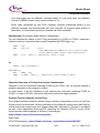
SSC.H2 Timing of flag SSCTIR (SSC Transmit Interrupt Request)
In master mode, the timing of SSCTIR is as follows:
When SSCTB has been written while the transmit shift register was empty (and the SSC
is enabled), flag SSCTIR is set to '1' directly after completion of the write operation,
independent of the selected baud rate. When the transmit shift register is not empty
when SSCTB was written, SSCTIR is set to '1' after the last latching edge of SCLK (= 1/
2 bit time before the first shifting edge of the next character). See also e.g. C167CR
User's Manual V3.1, p. 12-5.
The following diagram shows these relations in an example for a data transfer in master
mode with SSCPO = 0 and SSCPH = 0. It is assumed that the transmit shift register is
empty at the time the first character is written to SSCTB:
C164CM-4EF, Step (E)ES-AB, AB
20/27
es, V1.1, 2005-07-05
Errata Sheet
Application Hints
write to SSCTB, first character
write to SSCTB, next character
SCLK
MTSR
Bit 0
Bit n
Bit 1
SSCTIR = 1
SSCTIR = 1
Figure 3
Bit 0
SSCTB Timing
Typically, in interrupt driven systems, no problems are expected from the modified timing
of flag SSCTIR. However, when flag SSCTIR is polled by software in combination with
other flags which are set/cleared at the end or at the beginning of a transfer (e.g.
SSCBSY), the modified timing may have an effect.
Another situation where a different system behaviour may be noticed is the case when
only one character is transferred by the PEC into the transmit buffer register SSCTB. In
this case, 2 interrupt requests from SSCTIR are expected: the 'PEC COUNT = 0'
interrupt, and the 'SSCTB empty' interrupt:
When the PEC transfer is performed with sufficient margin to the next clock tick from the
SSC baud rate generator, and no higher priority interrupt request has occurred in the
meantime, the 'PEC COUNT = 0' interrupt will be acknowledged before the 'SSCTB
empty' interrupt request is generated, i.e. two interrupts will occur based on these
events. However, when the PEC transfer takes place relatively close before the next
clock tick from the SSC baud rate generator, or a higher priority interrupt request has
occurred while the PEC transfer is performed, the 'PEC COUNT = 0' interrupt may not
be acknowledged before the 'SSCTB empty' interrupt request is generated, such that
effectively only one interrupt request will be generated for two different events.
In order to achieve a defined and systematic behavior with all device steps, the SSC
receive interrupt, which is generated at the end of a character transmission, may be used
instead of the SSC transmit interrupt.
C164CM-4EF, Step (E)ES-AB, AB
21/27
es, V1.1, 2005-07-05
Errata Sheet
Application Hints
CAN.H1 Note on Interrupt Register Behaviour of the CAN module
Due to the internal state machine of the CAN module, a specific delay has to be
considered between resetting INTPND and reading the updated value of INTID. See
Application Note AP2924 "Interrupt Register behaviour of the CAN module ..." on:
Infineon Microcontroller Products: www.infineon.com/16-bit-microcontrollers
AP 2924 V01:
http://www.infineon.com/cgi/ecrm.dll/ecrm/scripts/
public_download.jsp?oid=10042&parent_oid=-8984
EMUL.H1 Adapt Mode setting for emulation of devices in Single Chip Mode
In Adapt Mode all target device pins are in high impedance state. This mode is mainly
used for deactivation of the soldered device while an emulator probe is connected. In
single chip mode (EA = 1) Adapt Mode can not be selected via PORT0 (P0L.1) during
reset, because PORT0 is not evaluated in this mode.
Recommendation:
• use no target device or a dummy device (package without silicon on the PCB) for
emuation or
• use the target device on the PCB and:
– provide a possibility to set target device pins EA and P0L.1 to "0" during reset (now
the adapt mode is enabled on the target device) and
– disconnect pin EA from the emulator probe and
– set the EA pin on the emulator-probe to "1" to configure the emulator in single chip
mode.
OTP.H1 OTP Read access in CHM Mode delivers Zeros only
In CHM mode the ROM-bus interface has no access to OTP (the OTP module is in a
special mode for programming). In this mode the OTP contents can be checked by the
verify sequence only. See e.g. C164CI User's Manual: Memory Organization - OTP
Memory Programming - OTP Programming Example: "ALT_VERIFY".
BSL.H1 Bootstrap Loader: Baudrate Detection in Single Chip Boot Mode
In single chip boot mode (Pin EA = 1) the bootstrap loader mode is detected during
hardware reset when pin RD is tied to low.
In this mode fCPU = fOSC / 2 (default configuration) and can be controlled via register
RSTCON. In case of a desired PLL mode (e.g. with a PLL factor of 5), fCPU in bootstrap
C164CM-4EF, Step (E)ES-AB, AB
22/27
es, V1.1, 2005-07-05
Errata Sheet
Application Hints
loader mode is 10 times slower than in normal running mode. So a communication with
an external host starts with a baudrate related to fCPU = fOSC / 2. It is recommended to
establish a 2nd level loader which adapts fCPU and baudrate to a convenient
transmission rate.
MainOsc.H1 Main Oscillator Type_LP2: Negative Resistance and Start-up
Reliability
Compared to other C16x microcontrollers the gain of the on-chip oscillator (Type_LP2)
is slightly different. It is recommended to check the negative resistance and the start-up
reliability of the oscillator circuit in the original application. Please refer to the limits
specified by the quartz crystal or ceramic resonator supplier.
See also Application Note AP2420 'Crystal Oscillator of the C500 and C166
Microcontroller Families' and Application Note AP2424 'Ceramic Resonator Oscillators
of the C500 and C166 Microcontroller Families'.
Infineon Microcontroller Products: www.infineon.com/16-bit-microcontrollers
AP2420: www.infineon.com/cgi/ecrm.dll/ecrm/scripts/
public_download.jsp?oid=9746&parent_oid=-8984
AP2424: www.infineon.com/cgi/ecrm.dll/ecrm/scripts/
public_download.jsp?oid=9745&parent_oid=-8984
MainOsc.H2 Maximum Oscillator Frequency = 16 MHz (Main: Type_LP2)
The main oscillator is optimized for oscillation with a crystal within a frequency range of
4...16 MHz. When driven by an external clock signal it will accept the specified frequency
range (see Data Sheet, AC Characteristics, tables ’Clock Generation Modes’ and
’External Clock Drive Characteristics’). Operation at lower input frequencies is possible
but is guaranteed by design only (not 100% tested) (see Data Sheet, AC Characteristics,
table ’External Clock Drive Characteristics’).
OWD.H2 Oscillator Watchdog and Prescaler Mode
The OWD replaces a missing oscillator clock signal with the PLL clock signal (base
frequency).
In direct drive mode the PLL base frequency is used directly (fCPU = 2...5 MHz).
In prescaler mode the PLL base frequency is divided by 2 (fCPU = 1...2.5 MHz).
C164CM-4EF, Step (E)ES-AB, AB
23/27
es, V1.1, 2005-07-05
Errata Sheet
Application Hints
ISNC.H1 Maintenance of ISNC register
The RTC and PLL interrupts share one interrupt node (XP3IC). If an interrupt request
occurs the request bit in the Interrupt Subnode Control register has to be checked and
cleared by software. To avoid a collision with the next hardware interrupt request of
same source it is recommended to clear the request and the enable bit first and then to
set the enable bit again.
Example for an XP3 interrupt service routine (for Tasking C compiler):
...
if (PLLIR)
{
_bfld (ISNC, 0x000C, 0x0000);
_putbit (1, ISNC, 3);
...
}
if (RTCIR)
{
_bfld (ISNC, 0x0003, 0x0000);
_putbit (1, ISNC, 1);
...
}
...
// clear PLLIE and PLLIR
// set PLLIE
// further actions concerning PLL/OWD
// clear RTCIE and RTCIR
// set RTCIE
// further actions concerning RTC
Example for an XP3 interrupt service routine (in assembly language):
...
EXTR
JNB
EXTR
#1
PLLIR, no_pll_request
#2
; no further interruption of this
;
sequence possible
BFLDL ISNC, #0Ch, #00h
; clear PLLIE and PLLIR
BSET
PLLIE
; set PLLIE
...
; further actions concerning PLL/OWD
no_pll_request:
EXTR
#1
JNB
RTCIR, no_rtc_request
EXTR
#2 ; no further interruption of this sequence possible
BFLDL ISNC, #03h, #00h
; clear RTCIE and RTCIR
BSET
RTCIE
; set RTCIE
...
; further actions concerning RTC
no_rtc_request:
...
C164CM-4EF, Step (E)ES-AB, AB
24/27
es, V1.1, 2005-07-05
Errata Sheet
Documentation Update
5
Documentation Update
INT.D2 Data Sheet V1.0 - Special Function Registers Overview
In contrast to Table 7 (Data Sheet V1.0, page 33...) the following CCxIC registers are
not implemented:
CC20IC, CC21IC, CC22IC, CC23IC, CC28IC, CC29IC, CC30IC and CC31IC, the
following CCxIC registers are additionally implemented: CC10IC, CC11IC. See also
Table 3 C164CM Interrupt Nodes (page 17).
Application Hint:
Due to the fact that CC28 ... 31 and fast external interrupts 0 ... 3 share the same pins
the missing interrupt nodes can be replaced:
Instead of the missing interrupt nodes for the CAPCOM registers 28 ... 31 the fast
external interrupts 0 ... 3 can be used if the correspondent pin is used as capture input
or compare output (compare modes 1 and 3). In this case the interrupt requesting edge
is selected in register EXICON, interrupt enable and level in register CC8IC ... CC11IC.
The dedicated interrupt vectors are CC8INT ... CC11INT, see Table 3 on page 17.
PLL.D1 PLL goes to Unlocked State after Configuration
When the PLL is (re-)configured via software by writing to register RSTCON, the PLL
goes to an unlocked state first (CLKLOCK = SYSCON2.15 = 0) and the PLL interrupt
request is set (flag PLLIR = ISNC.3 = 1) in the following cases:
• SW configuration of a PLL mode after single chip mode reset (pin EA is High) when a
PLL configuration is selected in bitfield CLKCFG (RSTCON.15 … 13), i.e. all
selections except 001B and 011B.
• SW re-configuration of a PLL mode in bitfield CLKCFG (RSTCON.15 … 13), i.e. all
selections except 001B and 011B.
When the PLL is locked again, bit CLKLOCK (SYSCON2.15) is set.
A re-configuration of register RSTCON with the same CLKCFG setting does not
influence the PLL.
In direct drive and prescaler mode (bitfield CLKCFG = RSTCON.15 … 13 = 001B or
011B) the PLL cannot lock and bit CLKLOCK in register SYSCON2 remains cleared.
Note: If PLLIR is set directly after reset the clock system is running on PLL base
frequency (or PLL base frequency / 2) and fOSC is missing or was unstable during
reset. Switching to SDD mode in this state could stop the system.
To avoid an unintentional PLL interrupt during this SW configuration of RSTCON, it is
recommended to disable the PLL interrupt while the PLL is in unlocked state.
C164CM-4EF, Step (E)ES-AB, AB
25/27
es, V1.1, 2005-07-05
Errata Sheet
Documentation Update
The example program for PLL modes shown below assumes that instruction EINIT has
not been executed yet. After EINIT, unlock sequences must be used to change RSTCON
and SYSCON2.
To avoid a deadlock situation, the wait_for_CLKLOCK loop should be terminated after a
timeout (before the WDT reset occurs).
JB
PLLIR, osc_clock_missing ; no osc clock before configuration
; is done, jump to emergency routine,
; don’t select SDD mode!
disable_PLL_interrupt:
EXTR #2
BCLR XP3IE
; disabled by default after reset
BCLR PLLIE
; ISNC.3, disabled by default after reset
change_PLL_configuration:
MOV
R4, #0000110100000000b ; PLL * 2.5, no CS, no SEG addr. lines
MOV
RSTCON, R4
; memory addressing mode only
;
EXTR
#2
MOV
SYSCON2, #0400h
MOV
SYSCON2, #0000h
...
;
;
;
;
;
(after EINIT unlock sequences are
required for RSTCON and SYSCON2)
SDD / 1 mode: enable RSTCON setting
PLLIR is set when PLL mode is changed
basic clock mode: activate setting
some instructions while clock is not at final state
wait_for_CLKLOCK:
EXTR #1
JNB
SYSCON2.15, wait_for_CLKLOCK ; timeout recommended
PLL_locked:
enable_PLL_interrupt:
EXTR #3
MOV
XP3IC, #0077h
BFLDL ISNC, #0Ch, #00h
BSET PLLIE
;
...
;
;
;
;
clear requests, enable XP3 interrupt,
int. level 13, group level 3
clear PLLIE and PLLIR
enable PLL interrupt
stable PLL clock
C164CM-4EF, Step (E)ES-AB, AB
26/27
es, V1.1, 2005-07-05
Errata Sheet
Documentation Update
PACKAGE.D1 P-TQFP64-8 Package used
The C164CM-4EF is delivered in the P-TQFP64-8 package. The Data Sheet V1.0, May
2001 erroneously refers to P-TQFP64-4 (page 63).
However, the P-TQFP64-4 package was never used for manufacturing. Also, both
packages have identical mechanical dimensions.
VIH.D1 Input High Voltage at Pin EA
The pin EA has a special structure to allow the usage as VPP pin (11.5 V) in OTP
programming mode. As a consequence the input levels at EA are not according TTL
specification.
In contrast to Table ’DC Characteristics’ (Data Sheet V1.0, page 42) EA belongs to
parameter VIH2 instead of VIH.
Parameter
Symbol
Limit Values
min.
max.
Unit Test
Condition
Input high voltage (TTL, all except VIH SR 0.2 VDD
RSTIN, XTAL1, EA)
+ 0.9
VDD +
0.5
V
–
VIH2 SR 0.7 VDD
VDD +
0.5
V
–
Input high voltage (XTAL1, EA)
ID-Registers
Register: IDMANUF IDCHIP
Device
IDMEM
IDPROG IDMEM2
F07CH
F07AH
F078H
F076H
C164CM-4E
Step Address: F07EH
-AA
1820H
1F01H
4008H
9340H
0000H
C164CM-4E
-AB
1F02H
4008H
9340H
0000H
1820H
Product and Test Engineering Group, Munich
C164CM-4EF, Step (E)ES-AB, AB
27/27
es, V1.1, 2005-07-05