1
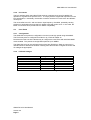
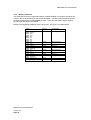
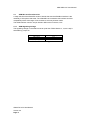
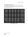
ADM-XRC-5LX
PCI Mezzanine Card
User Guide
Version 2.0
ADM-XRC-5LX User Manual
Copyright © 2006, 2007, 2008 Alpha Data Parallel Systems Ltd. All rights
reserved.
This publication is protected by Copyright Law, with all rights reserved. No
part of this publication may be reproduced, in any shape or form, without prior
written consent from Alpha Data Parallel Systems Limited
Alpha Data
4 West Silvermills Lane
Edinburgh EH3 5BD
UK
Alpha Data
2570 North First Street, Suite 440
San Jose, CA 95131
USA
Phone:
Fax:
Email:
Phone: (408) 467 5076
Fax:
(866) 820 9956
Email: [email protected]
+44 (0) 131 558 2600
+44 (0) 131 558 2700
[email protected]
ADM-XRC-5LX User Manual
Version 2.1
ADM-XRC-5LX User Manual
Table of Contents
1.
2.
3.
4.
5.
6.
Introduction ........................................................................................................................1
1.1.
Specifications ............................................................................................................1
Hardware Installation .........................................................................................................2
2.1.
Motherboard requirements........................................................................................2
2.2.
Handling instructions.................................................................................................2
2.3.
Installing the ADM-XRC-5LX onto a PMC motherboard...........................................2
2.4.
Installing the ADM-XRC-5LX if fitted to an ADC-PMC..............................................2
Software Installation...........................................................................................................2
Board Description ..............................................................................................................3
4.1.
Local Bus...................................................................................................................4
4.2.
Flash Memory............................................................................................................5
4.2.1.
Board Control Flash..........................................................................................5
4.2.2.
User FPGA Flash .............................................................................................5
4.3.
Health Monitoring ......................................................................................................5
4.4.
JTAG .........................................................................................................................6
4.5.
Clocks........................................................................................................................7
4.5.1.
LCLK.................................................................................................................7
4.5.2.
MCLK................................................................................................................8
4.5.3.
REFCLK ...........................................................................................................8
4.5.4.
XRM Clocks......................................................................................................8
4.5.5.
Rear (Pn4) Clocks ............................................................................................8
4.5.6.
PCI Clocks........................................................................................................9
4.6.
User FPGA ................................................................................................................9
4.6.1.
Configuration ....................................................................................................9
4.6.2.
I/O Bank Voltages.............................................................................................9
4.6.3.
Memory Interfaces..........................................................................................10
4.7.
XRM Bus and Front Panel I/O.................................................................................11
4.7.1.
XRM Signalling Voltage..................................................................................11
4.7.2.
XRM Interface – Connector Pinout.................................................................12
4.8.
Pn4 I/O ....................................................................................................................15
4.8.1.
Pn4 Signalling Voltage ...................................................................................16
XRM IO146 Interface .......................................................................................................17
Revision History ...............................................................................................................19
ADM-XRC-5LX User Manual
Version 2.1
ADM-XRC-5LX User Manual
Table of Tables
Table 1 Local Bus Interface Signal List .................................................................................... 4
Table 2 Voltage and Temperature Monitors............................................................................. 6
Table 3 XRM Bus Regional Clocks .......................................................................................... 8
Table 4 Rear (Pn4) Regional Clocks........................................................................................ 8
Table 5 User FPGA I/O Bank Voltages .................................................................................... 9
Table 6 DDR Memory Bank Configuration ............................................................................. 10
Table 7 XRM I/O Voltage Selection........................................................................................ 11
Table 8 XRM Interface - part 1 ............................................................................................... 12
Table 9 XRM Interface - part 2 ............................................................................................... 13
Table 10 XRM Interface - part 3 ............................................................................................. 14
Table 11 Pn4 to FPGA Assignments...................................................................................... 15
Table 12 Pn4 Voltage Selection ............................................................................................. 16
Table 13 IO146 Mictor Connector Pins 1 - 38........................................................................ 17
Table 14 IO146 Mictor Connector Pins 39 - 76...................................................................... 17
Table 15 IO146 Mictor Connector Pins 77 – 114 ................................................................... 18
Table 16 IO146 Mictor Connector Pins 115 - 152.................................................................. 18
Table of Figures
Figure 1
Figure 2
Figure 3
Figure 4
ADM-XRC-5LX Block Diagram .................................................................................. 3
Local Bus Interface .................................................................................................... 4
JTAG Header ............................................................................................................. 6
Clock Structure........................................................................................................... 7
ADM-XRC-5LX User Manual
Version 2.1
ADM-XRC-5LX User Manual
1.
Introduction
The ADM-XRC-5LX is a high performance PCI Mezzanine Card (PMC) designed for
supporting development of applications using the Virtex-5LX series of FPGAs from Xilinx.
The card uses an FPGA PCI bridge developed by Alpha-Data supporting PCI-X and PCI. A
high-speed multiplexed address/data bus connects the bridge to the target (user) FPGA.
1.1.
Specifications
The ADM-XRC-5LX supports high performance PCI-X / PCI operation without the need to
integrate proprietary cores into the user FPGA.
•
Physically conformant to IEEE P1386-2001 Common Mezzanine Card standard
•
High performance PCI and DMA controllers
•
Local bus speeds of up to 80 MHz
•
Four banks of 64Mx32 DDRII SDRAM (1GB total)
•
User clock programmable between 20MHz and 500MHz
•
Stable low-jitter 200MHz clock for precision IO delays
•
User front panel adapter with up to 146 free IO signals
•
User rear panel PMC connector with 64 free IO signals
•
Programmable 2.5V or 3.3V I/O on front and rear interfaces
•
Supports 3.3V PCI or PCI-X at 64 bits
ADM-XRC-5LX User Manual
Version 2.0
Page 1
ADM-XRC-5LX User Manual
2.
Hardware Installation
This chapter explains how to install the ADM-XRC-4 (LX/SX) onto a PMC motherboard.
2.1.
Motherboard requirements
The ADM-XRC-5LX supports 3.3V only signalling on the PCI Bus. It is not compatible with
systems that use 5V signalling.
The ADM-XRC-5T1 must be installed in a PMC motherboard that supplies +5.0V and +3.3V
power to the PMC connectors. Ensure that the motherboard satisfies this requirement before
powering it up. +12V and -12V may also be required for certain XRM modules.
2.2.
Handling instructions
Observe SSD precautions when handling the cards to prevent damage to components by
electrostatic discharge.
Avoid flexing the board.
2.3.
Note:
Installing the ADM-XRC-5LX onto a PMC motherboard
This operation should not be performed while the PMC motherboard is powered up.
The ADM-XRC-4 (LX/SX) must be secured to the PMC motherboard using M2.5 screws in
the four holes provided. The PMC bezel through which the I/O connector protrudes should be
flush with the front panel of the PMC motherboard.
2.4.
Installing the ADM-XRC-5LX if fitted to an ADC-PMC
The ADM-XRC-4 (LX/SX) can be supplied for use in standard PC systems fitted to an ADCPMC carrier board. The ADC-PMC can support up to two PMC cards whilst maintaining host
PC PCI compatibility. If you are using a ADC-PMC refer to the supplied documentation for
information on jumper settings. All that is required for installation is a PCI slot that has enough
space to accommodate the full-length card. The ADC-PMC is compatible with 5V and 3V PCI
(32 and 64 bit) and PCI-X slots.
It should be noted that the ADC-PMC uses a standard bridge to provide a secondary PCI bus
for the ADM-XRC-4 (LX/SX) and that some older BIOS code does not set up these devices
correctly. Please ensure you have the latest version of BIOS appropriate for your machine.
3.
Software Installation
Please refer to the SDK installation CD. The SDK contains drivers, examples for host control
and FPGA design and comprehensive help on application interfacing.
ADM-XRC-5LX User Manual
Version 2.0
Page 2
ADM-XRC-5LX User Manual
4.
Board Description
The ADM-XRC-5LX follows the architecture of the ADM-XRC series and decouples the
“target” FPGA from the PCI interface, allowing user applications to be designed with minimum
effort and without the complexity of PCI design.
A separate Bridge / Control FPGA interfaces to the PCI bus and provides a simpler Local Bus
interface to the target FPGA. It also performs all of the board control functions including the
configuration of the target FPGA, programmable clock setup and the monitoring of on-board
voltage and temperature.
DDR2 SDRAM and serial flash memory connect to the target FPGA and are supported by
Xilinx or third party IP.
IO functionality is provided using XRM modules connecting to a 180 pin SAMTEC QSH
connector.
Flash
Memory
(16MB)
Bridge
Config
Pn1
Pn2
Pn3
PCI-X /
PCI64/66
Pn4
Bridge / Control FPGA
Virtex4 LX25
Programmable
Clocks
Local Bus (64 bit)
User FPGA
Virtex5
LX50/80/110
Serial Flash
(4MB)
Rear I/O (64 bit)
JTAG
System
Monitor
(LM87)
Power
Conversion
DDR2
SDRAM
(256MB)
DDR2
SDRAM
(256MB)
Figure 1 ADM-XRC-5LX Block Diagram
ADM-XRC-5LX User Manual
Version 2.0
Page 3
XRM
Bus
(146 bit)
DDR2
SDRAM
(256MB)
DDR2
SDRAM
(256MB)
Front
I/O
(XRM)
ADM-XRC-5LX User Manual
4.1.
Local Bus
The ADM-XRC-5LX implements a multi-master local bus between the bridge and the target
FPGA using a 32- or 64-bit multiplexed address and data path. The bridge design is
asynchronous and allows the local bus to be run faster or slower than the PCI bus clock to
suit the requirements of the user design.
PCI
Bus
Bridge/Control
FPGA
Virtex4 LX25
lad_l[63:0]
lbe_l[7:0]
lads_l
lblast_l
lbterm_l
lready_l
lwrite
ldreq_l[3:0]
ldack_l[3:0]
User FPGA
Virtex5
LX55/80/110
fhold
fholda
lreset_l
lclk
Figure 2 Local Bus Interface
Signal
lad[0:63]
lbe_l[0:7]
lads_l
lblast_l
lbterm_l
lready_l
lwrite
ldreq_l[0:3]
ldack_l[0:3]
fhold
fholda
lreset_l
lclk
Type
bidir
bidir
bidir
bidir
bidir
bidir
bidir
unidir
unidir
unidir
unidir
unidir
unidir
Purpose
Address and data bus.
Byte qualifiers
Indicates address phase
Indicates last word
Indicates ready and requests new address phase
Indicates that target accepts or presents new data
Indicates a write transfer from master
DMA request from target to bridge
DMA acknowledge from bridge to target
Target bus request
Bridge bus acknowledge
Reset to target
Clock to synchronise bridge and target
Table 1 Local Bus Interface Signal List
ADM-XRC-5LX User Manual
Version 2.0
Page 4
ADM-XRC-5LX User Manual
4.2.
Flash Memory
The ADM-XRC-5LX is fitted with two separate Flash memories: one connected to the Bridge /
Control FPGA and the other to the User FPGA.
4.2.1. Board Control Flash
An Intel PC28F256P30 flash memory is used for storing a configuration bitstream for the User
FPGA. Once the Bridge / Control FPGA is configured, it checks for a valid bitstream in flash
and, if present, automatically loads it into the User FPGA. This process can be inhibited by
setting a jumper on the JTAG connector. See the description of the “FBS” signal in Section
4.4 for further information.
Access to this flash device is only possible through control logic registers. The flash is not
directly mapped onto the local bus.
Programming, erasing and verification of the flash are supported by the ADM-XRC SDK and
driver. Utilities are provided to load bitstreams into the flash. These also verify the bitstream
is compatible with the target FPGA.
4.2.2. User FPGA Flash
An ST M25P32 flash memory with SPI interface is connected to the User FPGA for the
storage of application-specific information.
Note: This device is not connected to the SPI configuration pins on the User FPGA and
cannot be used for configuration.
4.3.
Health Monitoring
The ADM-XRC-5LX has the ability to monitor temperature and voltage of key parts of the
PMC to maintain a check on the operation of the board. The monitoring is implemented by a
National Semiconductor LM87 and is supported by the board control logic connected using
I2C.
The Control Logic scans the LM87 when instructed by host software and stores all current
voltage and temperature measurements in a blockram. This allows the values to be read
without the need to communicate directly with the monitor.
The following supplies and temperatures, as shown in Table 2, are monitored.
ADM-XRC-5LX User Manual
Version 2.0
Page 5
ADM-XRC-5LX User Manual
Monitor
1.0V
1.2V
1.8V
2.5V
5.0V
PCI_VIO
XRM_VCCI
O
Temp1
Temp2
Purpose
User FPGA Core Supply
Bridge FPGA Core Supply
Memories, User FPGA Memory I/O,
Local Bus I/O
Config CPLD Core Supply
Source voltage for Front, Rear I/O
Board Input Supply
Monitors the PCI signalling supply – VIO
Either 2.5V or 3.3V Front Panel I/O Voltage
User FPGA die temperature
LM87 on die temperature for board/ambient
Table 2 Voltage and Temperature Monitors
An application is provided in the SDK that permits the reading of the health monitor. The
typical output of the monitor is shown below, provided by the SYSMON program.
4.4.
JTAG
A JTAG header is provided to allow download of the FPGA using the Xilinx tools and serial
download cables. This also allows the use of ChipScope PRO ILA to debug an FPGA
design. It should be noted that four devices will be detected when the SCAN chain is
initialised.
TMS
TDI
TDO
TCK
FBS
GND
VCC
Figure 3 JTAG Header
The VCC supply provided on J5 to the JTAG cable is +2.5V and is protected by a poly fuse
with a rating of 350mA.
FBS
The FBS signal is an input to the control logic and provides control of the cold boot process.
By default with no link fitted, the control logic will load a bitstream from flash into the FPGA if
one is present. Shorting FBS to the adjacent GND pin will disable this process and can be
used to recover situations where rogue bitstreams have been stored in flash.
ADM-XRC-5LX User Manual
Version 2.0
Page 6
ADM-XRC-5LX User Manual
4.5.
Clocks
The ADM-XRC-5LX is provided with numerous clock sources, as shown in Figure 4 below:
PCI
Bus
PCI
RefClk
PCI-X
CLK
Bridge Cfg Ctl
(Coolrunner)
25.0 MHz
Osc
PCI
CLK
Bridge FPGA
(V4LX25)
REFCLK_200M
Ctl
LCLK
25.0 MHz
XTAL
200 MHz
Osc.
Local Bus
ICS8430
MCLK
MCLK
XRM_CLKIN
XRM
Connector
(Samtec)
Zero-delay
Buffer
(PLL)
Pn4 Connector
User FPGA
V5LX55/80/110
FF1153
CLK0 (P)
CLK1 (N)
CLK2 (P)
CLK3 (N)
CLK4 (P)
KEY
CLK5 (N)
Global Clock Inputs
Clock Capable I/O
CLK6 (P)
CLK7 (N)
Figure 4 Clock Structure
4.5.1. LCLK
The Local Bus can be used at up to 80 MHz and all timing is synchronised to LCLK between
the Bridge and User FPGAs. LCLK is generated from a 200MHz reference by a DCM within
the bridge FPGA. The minimum LCLK frequency (determined by the DCM specification) is
32MHz.
The LCLK frequency is set by writing to the board control logic. (See SDK for details and
example application).
Note: If the user FPGA application includes a DCM driven by LCLK (or one of the other
programmable clocks), the clock frequency should be set prior to FPGA configuration.
ADM-XRC-5LX User Manual
Version 2.0
Page 7
ADM-XRC-5LX User Manual
4.5.2. MCLK
MCLK is an LVPECL clock generated by an ICS8430-61 synthesiser with a base 25MHz
crystal. The synthesiser has two outputs of the same clock, one of which is routed to the
User FPGA whilst the other is routed to the XRM connector. Both are terminated using
LVPECL terminations.
MCLK can be programmed to between 20MHz and 500MHz.
4.5.3. REFCLK
In order to make use of the IODELAY features of Virtex™-5, a stable low-jitter clock source is
required to provide the base timing for tap delay lines in each IOB in the User FPGA. The
ADM-XRC-5LX is fitted with a 200MHz LVPECL (LVDS optional) oscillator connected to
global clock resource pins. This reference clock can also be used for application logic if
required.
4.5.4. XRM Clocks
Global Clock Input
The XRM interface provides a differential input to the User FPGA global clocking resources.
The default on-board terminations are suitable for an LVPECL clock.
Regional Clocks
The XRM interface provides 8 clock lines that can be either be used single-ended or as 4
LVDS differential pairs. These clocks are routed to Clock-Capable I/O on the User FPGA,
providing access to its regional clock capabilities.
Each clock pair is in a different clock region alongside 16 pairs of XRM bus signals, as shown
in Table 3 below:
XRM Clocks
0 & 1 (Pair 0)
2 & 3 (Pair 1)
4 & 5 (Pair 2)
6 & 7 (Pair 3)
FPGA Bank
26
22
18
14
XRM bus pairs
1 – 16
17 – 32
33 – 48
49 – 64
Table 3 XRM Bus Regional Clocks
4.5.5. Rear (Pn4) Clocks
There are no dedicated clock lines between the Pn4 connector and the user FPGA.
However, the following signal pairs are routed to clock-capable I/O on the User FPGA,
providing access to its regional clock capabilities.
FPGA Bank
11
13
Pn4 bus pairs
22, 23, 24 & 25
6, 7, 8 & 9
Table 4 Rear (Pn4) Regional Clocks
ADM-XRC-5LX User Manual
Version 2.0
Page 8
ADM-XRC-5LX User Manual
4.5.6. PCI Clocks
The PCI Interface within the bridge FPGA requires a regional clock input for 66MHz PCI
operation or a global clock input for PCI-X. To comply with the single-load requirement in the
PCI specification, a zero-delay clock buffer is used to route the PCI clock to the two different
clock inputs.
The clock buffer has a PLL with a minimum input frequency of 24MHz, potentially causing
problems in applications that use the PCI 33MHz mode with a slow clock. In this case, the
buffer can be removed to provide full PCI 33MHz compatibility.
4.6.
User FPGA
4.6.1. Configuration
The ADM-XRC-5LX performs configuration from the host at high speed using SelectMAP.
The FPGA may also be configured from flash or by JTAG via header J5.
Download from the host is the fastest way to configure the User FPGA with 8 bit SelectMAP
mode enabled. This permits a configuration speed of up to 40MB/s.
The ADM-XRC-5LX can be configured to boot the User FPGA from flash on power-up if a
valid bit-stream is detected in the flash. Booting from flash will also configure the clocks and
I/O voltages as appropriate.
4.6.2.
I/O Bank Voltages
Bank
0
5, 12, 15, 16, 19, 20, 23, 24
2
3, 4
11, 13
14, 18, 26, 22
6, 17, 21, 25
Voltage
2.5V
1.8V
1.8V
3.3V
2.5V or 3.3V
2.5V or 3.3V
1.8V
Description
Configuration I/F
DDRII DRAM I/O
SelectMAP I/F
Clocks, Serial Flash
Pn4 Interface
XRM Interface
Local Bus
Table 5 User FPGA I/O Bank Voltages
ADM-XRC-5LX User Manual
Version 2.0
Page 9
ADM-XRC-5LX User Manual
4.6.3. Memory Interfaces
The ADM-XRC-5LX has 4 independent banks of DDRII SDRAM. Each bank consists of two
memory devices in parallel to provide a 32 bit datapath. 1Gb Micron MT47H64M16 devices
are fitted as standard to provide 256MB per bank. The board will support higher capacity
devices when they become available.
Details of the signalling standards, bank numbers etc. are given in the tables below:
Name
Direction
I/O Standard
DDR1_ad[15:0],
DDR1_ba[2:0],
DDR1_rasn,
DDR1_casn,
DDR1_wen,
DDR1_csn,
DDR1_cke,
DDR1_odt
DDR1_ck0,
DDR1_ckn0
DDR1_dq[15:0]
DDR1_dm[1:0]
DDR1_dqs[1:0],
DDR1_dqsn[1:0]
DDR1_ck1,
DDR1_ckn1
DDR1_dq[31:16]
DDR1_dm[3:2]
DDR1_dqs[3:2],
DDR1_dqsn[3:2]
DDR1_read_en_out
DDR1_read_en_in
Output
SSTL18_I
Output
DIFF_SSTL18_II
BiDir
Output
BiDir
SSTL18_II
SSTL18_I
DIFF_SSTL18_II
Output
DIFF_SSTL18_II
BiDir
Output
BiDir
SSTL18_II
SSTL18_I
DIFF_SSTL18_II
Output
Input
Table 6 DDR Memory Bank Configuration
ADM-XRC-5LX User Manual
Version 2.0
Page 10
ADM-XRC-5LX User Manual
4.7.
XRM Bus and Front Panel I/O
A major benefit of the ADM-XRC series of boards that use the XRM Bus interface is the
versatility of I/O options that result. The ADM-XRC-5LX maintains this interface and thus
compatibility with a wide range of I/O modules to suit many diverse needs.
The XRM interface uses the 180 pin Samtec QSH series connector, CN1.
4.7.1. XRM Signalling Voltage
The signalling voltage on the XRM connector (and User FPGA Banks 14, 18, 22 & 26) is
selectable by jumper J6.
J6
Link p1 & p2
Link p3 & p4
Link p5 & p4
XRM I/O voltage
3.3V
2.5V
1.8V
Table 7 XRM I/O Voltage Selection
ADM-XRC-5LX User Manual
Version 2.0
Page 11
ADM-XRC-5LX User Manual
4.7.2. XRM Interface – Connector Pinout
The XRM interface is implemented on CN1, a 180 pin Samtec connector type QSH, with the
pin-out as detailed in tables Table 8 to Table 10.
In turn, the signals that connect to CN1 are provided in the main from three banks of the User
FPGA, Banks 9, 11 and 13. These banks share a common VCCO that can be 2.5V or 3.3V
powered, selectable under user control.
Signal
N_1
P_1
N_3
P_3
N_5
P_5
N_7
P_7
P_9
N_9
N_11
P_11
N_13
P_13
N_15
P_15
N_17
P_17
WIRE_S_1
+3.3V
+3.3V
+3.3V
+5V
+5V
VBAT
+12V
+12V
PRESENCE_L
XRM_TCK
XRM_TMS
FPGA Pin
AL6
AL5
AL4
AM5
AM6
AN7
AN8
AN9
AP7
AP6
AM17
AN17
AP12
AP11
AN14
AP14
AA11
AA10
AL8
Samtec Pin
1
3
5
7
9
11
13
15
17
19
21
23
25
27
29
31
33
35
37
39
41
43
45
47
49
51
53
55
57
59
Samtec Pin
2
4
6
8
10
12
14
16
18
20
22
24
26
28
30
32
34
36
38
40
42
44
46
48
50
52
54
56
58
60
FPGA Pin
AN4
AN5
AP5
AP4
AM7
AM8
AL10
AM10
AN10
AM11
AP17
AP16
AM15
AM16
AP15
AN15
AA9
AA8
AP9
AP10
Table 8 XRM Interface - part 1
ADM-XRC-5LX User Manual
Version 2.0
Page 12
Signal
N_2
P_2
P_4
N_4
N_6
P_6
N_8
P_8
P_10
N_10
N_12
P_12
P_14
N_14
P_16
N_16
N_18
P_18
CLK0
CLK1
XRM_SERID
RESERVED
XRM_VREF
XRM_VCCIO
XRM_VCCIO
XRM_VCCIO
-12V
XRM_TDI
XRM_TRST
XRM_TDO
ADM-XRC-5LX User Manual
Signal
N_19
P_19
N_21
P_21
N_23
P_23
N_25
P_25
P_27
N_27
N_29
P_29
N_31
P_31
CLK2
CLK3
WIRE_S_2
WIRE_S_3
CLK4
CLK5
N_33
P_33
WIRE_S_8
S_9
RESERVED
RESERVED
XRM_PECL_N
XRM_PECL_P
RESERVED
RESERVED
FPGA Pin
AB10
AB11
AJ6
AJ7
AH7
AG7
AH8
AG8
AE9
AF9
AK8
AK9
AH10
AJ10
AE8
AF8
AN13
AC8
AA4
AB5
W11
Y11
AH2
AE18
Samtec Pin
61
63
65
67
69
71
73
75
77
79
81
83
85
87
89
91
93
95
97
99
101
103
105
107
109
111
113
115
117
119
Samtec Pin
62
64
66
68
70
72
74
76
78
80
82
84
86
88
90
92
94
96
98
100
102
104
106
108
110
112
114
116
118
120
FPGA Pin
AB7
AB8
AD7
AE7
AC9
AD9
AC10
AD10
AG10
AF10
AG11
AF11
AE11
AD11
AH9
W7
AE4
AC3
Y9
W9
AG1
AG2
AF18
AG20
AH19
AF19
AF20
Table 9 XRM Interface - part 2
ADM-XRC-5LX User Manual
Version 2.0
Page 13
Signal
N_20
P_20
N_22
P_22
N_24
P_24
P_26
N_26
N_28
P_28
P_30
N_30
N_32
P_32
WIRE_S_4
WIRE_S_5
WIRE_S_6
WIRE_S_7
N_34
P_34
CLK6
CLK7
S_10
XRM_CLKIN_N
XRM_CLKIN_P
XRM_SDA
XRM_SCL
RESERVED
RESERVED
RESERVED
ADM-XRC-5LX User Manual
Signal
P_35
N_35
N_37
P_37
P_39
N_39
N_41
P_41
P_43
N_43
P_45
N_45
N_47
P_47
P_49
N_49
P_51
N_51
N_53
P_53
P_55
N_55
N_57
P_57
N_59
P_59
N_61
P_61
N_63
P_63
FPGA Pin
W10
V10
V5
W5
Y6
W6
W4
Y4
AD5
AD6
AH4
AJ4
AJ5
AK4
V4
V3
Y3
Y2
AA1
AB1
AC2
AD1
AE1
AF1
AK3
AK2
AM1
AL1
AL3
AM2
Samtec Pin
121
123
125
127
129
131
133
135
137
139
141
143
145
147
149
151
153
155
157
159
161
163
165
167
169
171
173
175
177
179
Samtec Pin
122
124
126
128
130
132
134
136
138
140
142
144
146
148
150
152
154
156
158
160
162
164
166
168
170
172
174
176
178
180
FPGA Pin
V9
V8
Y7
Y8
AA6
AA5
AC5
AB6
AE6
AF5
AG6
AF6
W1
V2
AH5
AG5
Y1
W2
AA3
AB3
AD2
AE2
AE3
AF3
AH3
AG3
AP2
AN2
AN3
AM3
Table 10 XRM Interface - part 3
ADM-XRC-5LX User Manual
Version 2.0
Page 14
Signal
P_36
N_36
P_38
N_38
P_40
N_40
N_42
P_42
N_44
P_44
N_46
P_46
P_50
N_50
N_48
P_48
N_52
P_52
N_54
P_54
N_56
P_56
N_58
P_58
N_60
P_60
N_62
P_62
N_64
P_64
ADM-XRC-5LX User Manual
4.8.
Pn4 I/O
Up to 32 pairs of differential or 64 single-ended signals are available on Pn4 and are sourced
from Banks 11 & 13 of the User FPGA. All of the signal traces are routed as 100 Ohm
differential pairs and each pair is matched in length. The worst case difference in trace length
between any two pairs is 10mm.
Signal
PN4_P1
PN4_N1
PN4_P3
PN4_N3
PN4_P5
PN4_N5
PN4_P7
PN4_N7
PN4_P9
PN4_N9
PN4_P11
PN4_N11
PN4_P13
PN4_N13
PN4_P15
PN4_N15
PN4_P17
PN4_N17
PN4_P19
PN4_N19
PN4_P21
PN4_N21
PN4_P23
PN4_N23
PN4_P25
PN4_N25
PN4_P27
PN4_N27
PN4_P29
PN4_N29
PN4_P31
PN4_N31
FPGA Pin
AN34
AN33
AL34
AL33
AK34
AK33
AH34
AJ34
AF33
AE33
AC32
AB32
AA34
Y34
W34
V34
U33
T34
T33
R34
L33
M32
L34 [CC]
K34 [CC]
J32 [CC]
H33 [CC]
E32
E33
C34
D34
B33
C33
Pn4 Pin
1
3
5
7
9
11
13
15
17
19
21
23
25
27
29
31
33
35
37
39
41
43
45
47
49
51
53
55
57
59
61
63
Pn4 Pin
2
4
6
8
10
12
14
16
18
20
22
24
26
28
30
32
34
36
38
40
42
44
46
48
50
52
54
56
58
60
62
64
FPGA Pin
AM33
AM32
AJ32
AK32
AD32
AE32
AF34
AE34
AC33
AB33
AC34
AD34
AA33
Y33
V33
V32
R33
R32
P32
N32
K33 [CC]
K32 [CC]
H34 [CC]
J34 [CC]
G33
F34
F33
E34
C32
D32
B32
A33
Signal
PN4_P2
PN4_N2
PN4_P4
PN4_N4
PN4_P6
PN4_N6
PN4_P8
PN4_N8
PN4_P10
PN4_N10
PN4_P12
PN4_N12
PN4_P14
PN4_N14
PN4_P16
PN4_N16
PN4_P18
PN4_N18
PN4_P20
PN4_N20
PN4_P22
PN4_N22
PN4_P24
PN4_N24
PN4_P26
PN4_N26
PN4_P28
PN4_N28
PN4_P30
PN4_N30
PN4_P32
PN4_N32
Table 11 Pn4 to FPGA Assignments
In Table 11, pins marked [CC] are clock capable and may be used to access the regional
clocking resources in the FPGA.
Banks 11 & 13 are fitted with resistors to allow DCI terminations on Pn4 signals.
ADM-XRC-5LX User Manual
Version 2.0
Page 15
ADM-XRC-5LX User Manual
4.8.1. Pn4 Signalling Voltage
User FPGA Banks 11 & 13 and Pn4 can use 3.3V or 2.5V signalling standards selectable by
switch SW2B.
SW2B
Open
Closed
Pn4 voltage
2.5V
3.3V
Table 12 Pn4 Voltage Selection
It should be noted that the switch does not directly route power to Banks 11 & 13. The link
position is monitored by the board control logic which, in turn, sets a power multiplexer to be
either 2.5V or 3.3V.
ADM-XRC-5LX User Manual
Version 2.0
Page 16
ADM-XRC-5LX User Manual
5.
XRM IO146 Interface
The following tables provide the user with information on the pin-out of the XRM-IO146 when
fitted to an ADM-XRC-5LX card.
The signal names P_1/N_1 etc are internal to the ADM-XRC-5LX. The important mapping is
between the Mictor pin and the FPGA pin.
Signal
FPGA Pin
Samtec
P_1
N_1
P_3
N_3
P_5
N_5
P_7
N_7
P_9
N_9
P_11
N_11
P_13
N_13
P_15
N_15
S_1
S_2
+5V
AL5
AL6
AM5
AL4
AN7
AM6
AN9
AN8
AP7
AP6
AN17
AM17
AP11
AP12
AP14
AN14
AL8
AN13
3
1
7
5
11
9
15
13
17
19
23
21
27
25
31
29
37
93
-
Mictor
Pin
1
3
5
7
9
11
13
15
17
19
21
23
25
27
29
31
33
35
37
Mictor
Pin
2
4
6
8
10
12
14
16
18
20
22
24
26
28
30
32
34
36
38
Samtec
FPGA Pin
Signal
6
8
4
2
12
10
16
14
18
20
24
22
26
28
30
32
38
40
90
AP5
AP4
AN5
AN4
AM8
AM7
AM10
AL10
AN10
AM11
AP16
AP17
AM15
AM16
AP15
AN15
AP9
AP10
AH9
P_4
N_4
P_2
N_2
P_6
N_6
P_8
N_8
P_10
N_10
P_12
N_12
P_14
N_14
P_16
N_16
CLK0
CLK1
S_4
Table 13 IO146 Mictor Connector Pins 1 – 38
Signal
FPGA Pin
Samtec
P_17
N_17
P_19
N_19
P_21
N_21
P_23
N_23
P_25
N_25
P_27
N_27
P_29
N_29
P_31
N_31
S_8
S_9
+5V
AA10
AA11
AB11
AB10
AJ7
AJ6
AG7
AH7
AG8
AH8
AE9
AF9
AK9
AK8
AJ10
AH10
AH2
AE18
35
33
63
61
67
65
71
69
75
73
77
79
83
81
87
85
105
107
-
Mictor
Pin
39
41
43
45
47
49
51
53
55
57
59
61
63
65
67
69
71
73
75
Mictor
Pin
40
42
44
46
48
50
52
54
56
58
60
62
64
66
68
70
72
74
76
Samtec
FPGA Pin
Signal
36
34
64
62
68
66
72
70
74
76
80
78
82
84
88
86
89
91
95
AA8
AA9
AB8
AB7
AE7
AD7
AD9
AC9
AC10
AD10
AF10
AG10
AG11
AF11
AD11
AE11
AE8
AF8
AC8
P_18
N_18
P_20
N_20
P_22
N_22
P_24
N_24
P_26
N_26
P_28
N_28
P_30
N_30
P_32
N_32
CLK2
CLK3
S_3
Table 14 IO146 Mictor Connector Pins 39 - 76
ADM-XRC-5LX User Manual
Version 2.0
Page 17
ADM-XRC-5LX User Manual
Signal
FPGA Pin
Samtec
P_33
N_33
P_35
N_35
P_37
N_37
P_39
N_39
P_41
N_41
P_43
N_43
P_45
N_45
P_47
N_47
S_5
S_6
+5V
Y11
W11
W10
V10
W5
V5
Y6
W6
Y4
W4
AD5
AD6
AH4
AJ4
AK4
AJ5
W7
AE4
103
101
121
123
127
125
129
131
135
133
137
139
141
143
147
145
92
94
-
Mictor
Pin
77
79
81
83
85
87
89
91
93
95
97
99
101
103
105
107
109
111
113
Mictor
Pin
78
80
82
84
86
88
90
92
94
96
98
100
102
104
106
108
110
112
114
Samtec
FPGA Pin
Signal
100
98
122
124
126
128
130
132
136
134
140
138
144
142
152
150
97
99
-
W9
Y9
V9
V8
Y7
Y8
AA6
AA5
AB6
AC5
AF5
AE6
AF6
AG6
AG5
AH5
AA4
AB5
P_34
N_34
P_36
N_36
P_38
N_38
P_40
N_40
P_42
N_42
P_44
N_44
P_46
N_46
P_48
N_48
CLK4
CLK5
+5V
Table 15 IO146 Mictor Connector Pins 77 – 114
Signal
FPGA Pin
Samtec
P_49
N_49
P_51
N_51
P_53
N_53
P_55
N_55
P_57
N_57
P_59
N_59
P_61
N_61
P_63
N_63
S_7
S_10
+5V
V4
V3
Y3
Y2
AB1
AA1
AC2
AD1
AF1
AE1
AK2
AK3
AL1
AM1
AM2
AL3
AC3
AF18
149
151
153
155
159
157
161
163
167
165
171
169
175
173
179
177
96
106
-
Mictor
Pin
115
117
119
121
123
125
127
129
131
133
135
137
139
141
143
145
147
149
151
Mictor
Pin
116
118
120
122
124
126
128
130
132
134
136
138
140
142
144
146
148
150
152
Samtec
FPGA Pin
Signal
146
148
156
154
160
158
164
162
168
166
172
170
176
174
180
178
102
104
-
W1
V2
W2
Y1
AB3
AA3
AE2
AD2
AF3
AE3
AG3
AH3
AN2
AP2
AM3
AN3
AG1
AG2
P_50
N_50
P_52
N_52
P_54
N_54
P_56
N_56
P_58
N_58
P_60
N_60
P_62
N_62
P_64
N_64
CLK6
CLK7
+5V
Table 16 IO146 Mictor Connector Pins 115 - 152
ADM-XRC-5LX User Manual
Version 2.0
Page 18
ADM-XRC-5LX User Manual
6.
Revision History
Date
Revision
Nature of Change
22-08-2006
1.0
First Release.
17-12-2007
1.1
Revised wording of motherboard power requirements.
16-01-2008
2.0
Updated to reflect changes to lclk and Front IO voltage
selection on Rev2 PCBs.
ADM-XRC-5LX User Manual
Version 2.0
Page 19