1
NANO-5050
NANO-ITX Board
User's Manual
Version 1.0
Copyright © Portwell, Inc., 2013. All rights reserved.
All other brand names are registered trademarks of their respective owners.
Preface
Table of Contents
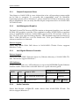
How to Use This Manual
Chapter 1 System Overview.......................................................................................................1-1
1.1 Introduction.................................................................................................................................. 1-1
1.2 Check List ..................................................................................................................................... 1-1
1.3 Product Specification .................................................................................................................. 1-1
1.4 System Configuration ................................................................................................................. 1-3
1.4.1 Mechanical Drawing......................................................................................................... 1-4
1.5 System Architecture .................................................................................................................... 1-5
Chapter 2 Hardware Configuration ...........................................................................................2-1
2.1 Jumper Setting ............................................................................................................................. 2-1
2.2 Connectors.................................................................................................................................... 2-2
Chapter 3 System Installation....................................................................................................3-1
3.1 Intel ® Atom TM Processor D2550 .............................................................................................. 3-1
3.2 Main Memory .............................................................................................................................. 3-1
3.3 Installing Single Board Computer............................................................................................. 3-1
3.3.1 Chipset Component Driver.............................................................................................. 3-2
3.3.2 IntelI®Integrated Graphics .............................................................................................. 3-2
3.3.3 Intel Gigabit Ethernet Controller .................................................................................... 3-2
3.3.4 Audio Controller ............................................................................................................... 3-2
3.4 Clear CMOS Operation............................................................................................................... 3-3
3.5 WDT Function.............................................................................................................................. 3-3
3.6 GPIO .............................................................................................................................................. 3-5
Chapter 4 BIOS Setup Information............................................................................................4-1
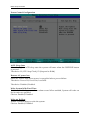
4.1 Entering Setup.............................................................................................................................. 4-1
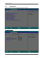
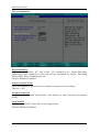
4.2 Main............................................................................................................................................... 4-2
4.3 Configuration............................................................................................................................... 4-3
4.4 Security ....................................................................................................................................... 4-20
4.5 Boot.............................................................................................................................................. 4-21
4.6 Exit............................................................................................................................................... 4-22
Chapter 5 Troubleshooting ........................................................................................................5-1
5.1 Hardware Quick Installation ..................................................................................................... 5-1
5.2 FQA ............................................................................................................................................... 5-2
Appendix A
Appendix B
Preface
How to Use This Manual
The manual describes how to configure your NANO-5050 system to meet various
operating requirements. It is divided into five chapters, with each chapter
addressing a basic concept and operation of Single Board Computer.
Chapter 1 : System Overview. Presents what you have in the box and give you an
overview of the product specifications and basic system architecture for this series
model of single board computer.
Chapter 2 : Hardware Configuration. Shows the definitions and locations of
Jumpers and Connectors that you can easily configure your system.
Chapter 3 : System Installation. Describes how to properly mount the CPU, main
memory and Compact Flash to get a safe installation and provides a programming
guide of Watch Dog Timer function.
Chapter 4 : BIOS Setup Information. Specifies the meaning of each setup
parameters, how to get advanced BIOS performance and update new BIOS. In
addition, POST checkpoint list will give users some guidelines of trouble-shooting.
Chapter 5 : Troubleshooting. Provides various useful tips to quickly get NANO5050 running with success. As basic hardware installation has been addressed in
Chapter 3, this chapter will basically focus on system integration issues, in terms of
backplane setup, BIOS setting, and OS diagnostics.
The content of this manual and EC declaration document is subject to change
without prior notice. These changes will be incorporated in new editions of the
document. Portwell may make supplement or change in the products described in
this document at any time.
Updates to this manual, technical clarification, and answers to frequently asked
questions will be shown on the following web site :
http://www.portwell.com.tw/.
System Overview
Chapter 1
System Overview
1.1
Introduction
Portwell Inc., a world-leading innovator in the Industrial PC (IPC) market and a member
of the Intel® Communications Alliance, has launched its new NANO-ITX form factor
based NANO-5050 for embedded system board (ESB) that offers a smaller footprint,
lower power consumption, robust computing power and with longevity support.
The NANO-5050 is specifically designed to operate at very low power consumption and
low heat, so it can be a truly fanless configuration and battery operated. Base on Intel®
System Controller Hub NM10, the NANO-5050 supports one DDR3 SODIMM socket up
to 4GB system memory and comes with one SATA II, one Mini-PCIe socket, triple
independent display by VGA, DP and 18/24-bit LVDS (dual display at the same time),
one gigabit Ethernet, one CF-SATA socket and Six USB 2.0 ports (two ports are on rear
IO). It also built with DC 12V or ATX 12V input.
Base on leading Intel® Atom solution, NANO-5050 is a compact and low power
dissipation board for Digital Signage, Digital Security Surveillance (DSS) and Medical
applications…etc.
1.2
Check List
The NANO-5050 package should cover the following basic items
3 One NANO-5050 NANO-ITX Main Board
3 One passive Heatsink
3 One Installation Resources CD-Title
3 One SATA cable
If any of these items is damaged or missing, please contact your vendor and keep all
packing materials for future replacement and maintain
1.3
Product Specification
z Main Processor
- On board Intel® ATOMTM D2550 1.86GHz processor
z Chipset
- Intel® System Controller Hub NM10
NANO-5050 User’s Manual
1-1
System Overview
z System BIOS
- Phoenix uEFI BIOS
z Main Memory
- One 204pin DDR3 SODIMM socket on board up to 4GB system memory
z Power input
- DC 12V input on rear I/O
- 4pin +12V power connector on board
- (DC 12V Jack and 4pin power connector can’t be used at the same time)
z Serial Port
- Support one RS232/422/485 port on-board connector (adjust by bios)
z USB Interface
- Support six USB 2.0 (Universal Serial Bus) ports, two on rear I/O and four on board
header for internal devices.
z SATA Interface
- Support one SATA II ports
z CF-SATA interface
- Support one CF-SATA socket
- Support both CF card and CF-SATA card
z Audio Interface
- Mic-In and Line-Out Audio Jack on rear I/O
z Watch Dog Timer
- Support WDT function through software programming for enable/disable and
interval setting
- General system reset
z Display
- Support triple independent display by DP (rear I/O), VGA (on-board connector)
and single channel 18/24-bit LVDS
- Only support dual display simultaneously
z On-board Ethernet LAN
- One Gigabit Ethernet (10/100/1000 Mbits/sec) LAN port using Intel 82583V PCIExpressx1 interface GbE Controller
- Support Wake on LAN function
z High Drive GPIO
- On-board programmable 8-bit Digital I/O interface
z Cooling Fans
- Support one 3-pin power connector for system fan
z System Monitoring Feature
- Monitor system temperature and major power sources.
z Outline Dimension (L x W)
- 120mm(4.72’’) x 120mm(4.72’’)
NANO-5050 User’s Manual
1-2
System Overview
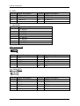
1.4
System Configuration
System Configuration
CPU Type
SBC BIOS
Memory
Intel® Atom™ CPU D2550 @1.86GHz L2:1024K
Portwell, Inc. NANO-5050 Rev.:R1.00.W2(12112012)
VGA Card
VGA Driver
LAN Card
LAN Driver
Audio Card
Audio Driver
Chip Driver
SATA HDD
Onboard Intel® Graphics Media Accelerator 3600 Series
Compact Flash
Apacer AP-CF001GP4CG-NR
USB CDROM
Power Supply
ASUS CB-5216A-U
Transcend DDR3 1066 SODIMM 4G*1 (hynix H5TQ2G83AFR)
Intel® Graphics Media Accelerator 3600 Series Ver:8.14.8.1075
Onboard Intel® 82583V Gigabit Network Connection
Intel® 82583V Gigabit Network Connection Ver:11.17.27.0
Onboard Realtek ALC886 High Definition Audio
Realtek ALC886 High Definition Audio Ver:6.0.1.6526
Intel® Chipset Device Software Ver:9.2.2.1029
Seagate ST3160316AS 160GB
FSP150-50PL1
z Power Consumption test: Run Burning Test V6.0
RUN time: 10 / 30 Minutes.
Full Loading
Item
Power ON
10Min
DC +12V
z Operating Temperature
0°C ~ 55°C
z Storage temperature
-20 ~ 85 °C
z Relative Humidity
0% ~ 95%, non-condensing
NANO-5050 User’s Manual
1.41
1.84
Full Loading
30Min
1.86
1-3
System Overview
1.4.1 Mechanical Drawing
NANO-5050 User’s Manual
1-4
System Overview
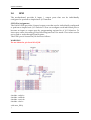
1.5
System Architecture
All of details operating relations are shown in NANO-5050 System Block Diagram.
NANO-5050
NANO-5050 User’s Manual
System Block Diagram
1-5
Hardware Configuration
Chapter 2
Hardware Configuration
This chapter gives the definitions and shows the positions of jumpers, headers and
connector. All of the configuration jumpers on NANO-5050 are in the proper
position. The default settings are indicated with a star sign (Ì).
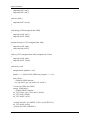
2.1
Jumper Setting
In the following sections, Short means covering a jumper cap over jumper pins;
Open or N/C (Not Connected) means removing a jumper cap from jumper pins.
Users can refer to Figure 2-1 for the Jumper allocations.
Figure 2-1
NANO-5050 User’s Manual
NANO-5050 Jumper and Connector Locations (Top)
2-1
Hardware Configuration
Figure 2-2
2.2
NANO-5050 Jumper and Connector Locations (Bottom)
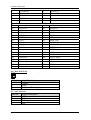
Connectors
I/O peripheral devices are connected to the interface connectors.
Connector
Function
J1
+12V DC adapter
J2
Line Out
J3
Mic In
J4
Display Port
J5
CRT display
J6
USB
J7
LAN
NANO-5050 User’s Manual
Remark
2-2
Hardware Configuration
J8
J9
J10
J11
J12
J13
J14
J15
J16
J17
J18
J19
J20
J21
J22
J23
J24
J25
JP1
JP2
JP3
reserve USB
reserve USB
8 bits GPIO
LPC debug port
Serial Port
+12V DC source
reserve
Mini PCIe
Rear side FAN
SATA power
LVDS pane
LED/Switch
SATA
SM Bus
Coin battery
Panel back light
PCIe x1
CF-SATA (button side)
Clean RTC(Default 1-2)
LVDS Power Level (Default 1-2)
LVDS Back-light enable level high/low (Default 1-2)
Pin Assignments of Connectors
J1 : reserve for +12V DC adapter
PIN No.
Signal Description
1
12V
2
GND
3
GND
J2 : Line Out
PIN No.
1
2
3
4
5
Signal Description
GND
Line Out L
GND
Jack Detect
Line Out R
NANO-5050 User’s Manual
2-3
Hardware Configuration
J3 : Mic In
PIN No.
1
2
3
4
5
Signal Description
GND
Mic In L
GND
Jack Detect
Mic In R
J4 : Display Port
PIN No.
1
3
5
7
9
11
13
15
17
19
Signal Description
Lane0+
Lane0GND
Lane2+
Lane2GND
CONFIG1
AUX_CH+
AUX_CHReturn for Power
PIN No.
2
4
6
8
10
12
14
16
18
20
Signal Description
GND
Lane1+
Lane1GND
Lane3+
Lane3CONFIG2
GND
Hot Plug
DP Power 3.3V/500mA
J5 : CRT Display
PIN No. Signal Description
1
RED
3
GREEN
5
BLUE
7
VSYNC
9
HSYNC
NANO-5050 User’s Manual
PIN No. Signal Description
2
DDCCLK
4
A_Ground
6
DDCDATA
8
D_Ground
10
DDC_VCC
2-4
Hardware Configuration
J6 : USB
PIN No. Signal Description
A1
+5V
A2
USBD0-1N
A3
USBD0-1P
A4
Ground
PIN No. Signal Description
B1
+5V
B2
USBD0-1N
B3
USBD0-1P
B4
Ground
J7 : LAN(RJ45)
PIN No.
Signal Description
1
L1_MDIP0
2
L1_MDIN0
3
L1_MDIP1
4
L1_MDIP2
5
L1_MDIN2
6
L1_MDIN1
7
L1_MDIP3
8
L1_MDIN3
J8/J9 : reserve USB
10
2
1
7
PIN No. Signal Description
1
+5V
3
USBD5
USBD+
7
GND
PIN No. Signal Description
2
+5V
4
USBD6
USBD+
8
GND
10
NC
J10 : 8 bits GPIO
PIN No.
1
3
5
7
9
Signal Description
GPIO0
GPIO1
GPIO2
GPIO3
GND
NANO-5050 User’s Manual
PIN No.
2
4
6
8
10
Signal Description
GPIO4
GPIO5
GPIO6
GPIO7
VCC
2-5
Hardware Configuration
J11 : LPC debug Po
10
2
1
7
PIN No.
1
3
5
7
Signal Description
LAD0
LAD1
LAD2
LAD3
PIN No.
2
4
6
8
10
Signal Description
+3.3V
RST#
LFRAME#
33MHzCLK
GND
PIN No.
2
4
6
8
Signal Description
Receive Data (RXD)
Data Terminal Ready (DTR)
Data Set Ready (DSR
Clear to Send (CTS)
J12 : Serial Port
RS-232 Mode:
PIN No. Signal Description
1
Data Carrier Detect (DCD)
3
Transmit Data (TXD)
5
GND
7
Request to Send (RTS)
9
Ring Indicator (RI
RS-422/485 Mode:
PIN No. Signal Description
1
TxD-/RxD3
RxD+(422 only)
5
GND
PIN No. Signal Description
2
TxD+/RxD
4
RxD-(422 only)
J13 : +12V DC Source
PIN No.
Signal Description
1
GND
2
GND
3
+12V
4
+12V
J14 : Reserve
J15 : Mini PCIe
PIN No. Signal Description
1
Wake#
3
Reserved
5
Reserved
NANO-5050 User’s Manual
PIN No.
2
4
6
Signal Description
3.3V
GND
1.5V
2-6
Hardware Configuration
7
9
11
13
15
17
19
21
23
25
27
29
31
33
35
37
39
41
43
45
47
49
51
CLKREQ#
GND
REFCLKREFCLK+
GND
Reserved
Reserved
GND
PE_R_0PE_R_0+
GND
GND
PE_T_0PE_T_0+
GND
Reserved
Reserved
Reserved
Reserved
Reserved
Reserved
Reserved
Reserved
8
10
12
14
16
KEY
18
20
22
24
26
28
30
32
34
36
38
40
42
44
46
48
50
52
Reserved
Reserved
Reserved
Reserved
Reserved
GND
Reserved
PERST#
+3.3Vaux
GND
1.5V
SMB_CLK
SMB_DAT
GND
USB_DUSB_D+
GND
LED_WAN#
LED_LAN#
LED_PAN#
1.5V
GND
3.3V
J16 : Rear Side FAN
12 3
PIN No.
1
2
3
Signal Description
Ground
+12V
Fan Speed Detecting signal
J17 : SATA Power
PIN No.
Signal Description
1
+12V
2
GND
3
GND
4
+5V
NANO-5050 User’s Manual
2-7
Hardware Configuration
J18 : LVDS Panel
PIN No.
Signal Description
1
LVDS_DATA0
3
LVDS_DATA1
5
LVDS_DATA2
7
LVDS_DATA3
9
LVDS_CLK
11
NC
13
NC
15
NC
17
NC
19
NC
21
LVDS_DDC_CLK
23
GND
25
GND
27
VDD_LVDS
29
NC
PIN No.
2
4
6
8
10
12
14
16
18
20
22
24
26
28
30
Signal Description
LVDS_DATA#0
LVDS_DATA#1
LVDS_DATA#2
LVDS_DATA#3
LVDS_CLK#
NC
NC
NC
NC
NC
LVDS_DDC_DATA
NC
GND
VDD_LVDS
VDD_LVDS
J19 : LED/Switch
PIN No.
Signal Description
1
WR_LED3
SUS_LED+
5
HDD_LED+
7
RST_BTN
9
GND
PIN No.
2
4
6
8
10
Signal Description
LVDS_DATA#0
LVDS_DATA#1
HDD_LED
GND
PWR_BTN
J20 : SATA
PIN No.
1
2
3
4
5
6
7
Signal Description
GND
DF_SATA_TX+0
DF_SATA_TX-0
GND
DF_SATA_RX-0
DF_SATA_RX+0
GND
J21 : SM BUS
PIN No.
Signal Description
1
SM_CLK
2
SM_DATA
3
GND
4
3.3V
NANO-5050 User’s Manual
2-8
Hardware Configuration
J22 : Coin Battery
PIN No.
Signal Description
1
Positive
2
Negative
J23 : Panel back light
PIN No.
Signal Description
1
+5V
2
GND/PWM
3
+12V
4
GND
5
BACKLIGH_EN/EN#
J24 : PCIe x 1
PIN No.
Signal Description
A1
SMBCLK
A2
+12V
A3
+12V
A4
GND
A5
DF_PCIE_TXP2
A6
DF_PCIE_TXN2
A7
DF_PCIE_RXP2
A8
DF_PCIE_RXN2
A9
+3.3V
A10
+3.3V
A11
RST#
A12
GND
A13
DF_ PCIE_CLKP1
A14
DF_ PCIE_CLKN1
A15
GND
A16
DF_PCIE_RXP1
A17
DF_PCIE_RXN1
A18
GND
PIN No.
B1
B2
B3
B4
B5
B6
B7
B8
B9
B10
B11
B12
B13
B14
B15
B16
B17
B18
Signal Description
+12V
+12V
+12V
GND
DF_ PCIE_CLKP
DF_ PCIE_CLKN2
GND
+3.3V
CLKREQ2#
+3.3V_AUX
PCIE_WAKE#
SMBDATA
GND
DF_PCIE_TXP1
DF_PCIE_TXN1
GND
CLKREQ1#
GND
J25 : CF-SATA
PIN No.
Signal Description
1
GND
2
D3
3
D4
4
D5
5
D6
6
D7
7
CS0#
8
GND
9
ATASEL#
PIN No.
26
27
28
29
30
31
32
33
34
Signal Description
CD1#
D11
D12
D13
D14
D15
CS1#
VS1#
IOR#
NANO-5050 User’s Manual
2-9
Hardware Configuration
10
11
12
13
14
15
16
17
18
19
20
21
22
23
24
25
SATA_TX+
SATA_TXGND
VCC
GND
SATA_RXSATA_RX+
GND
A2
A1
A0
D0
D1
D2
IOCS16#
CD2#
35
36
37
38
39
40
41
42
43
44
45
46
47
48
49
50
IOW#
WE#
INTR
VCC
CSEL#
VS2#
RESET#
IORDY
DMARQ
DMACK#
DASP#
PDIAG#
D8
D9
D10
GND
JP1 : Clean RTC
PIN No.
Function
1-2
Positive
2-3
Negative
JP2 : Panel Power Level
PIN No.
Process Selection
1-2
3.3V Ì
3-4
5V
5-6
12V
JP3 : Backlight enable signal type
PIN No.
Process Selection
1-2
High enable Ì
2-3
Low enable
NANO-5050 User’s Manual
2-10
System Installation
Chapter 3
System Installation
This chapter provides you with instructions to set up your system. The additional
information is enclosed to help you set up onboard PCI device and handle Watch
Dog Timer (WDT) and operation of GPIO in software programming.
3.1
Intel ® Atom TM Processor D2550
Passively-cooled, soldered-down Dual-Core Intel ® Atom™ processor D2550 with
integrated graphics and integrated memory controller that’s suitable for fanless
system and low-watt design.
3.2
Main Memory
NANO-5050 provide 1 x 204-pin SO-DIMM sockets which supports 800/1066 MHz
DDR3-SDRAM as main memory, Non-ECC (Error Checking and Correcting), nonregister functions. The maximum memory size can be up to 4GB capacity. Memory
clock and related settings can be detected by BIOS via SPD interface.
Watch out the contact and lock integrity of memory module with socket, it will
impact on the system reliability. Follow normal procedures to install memory
module into memory socket. Before locking, make sure that all modules have been
fully inserted into the card slots.
Note: DDR3 1333 MHz and DDR3 1600 MHz memory will run at 1066 MHz
3.3
Installing Single Board Computer
To install your NANO-5050 into standard chassis or proprietary environment, please
perform the following:
Step 1 : Check all jumpers setting on proper position
Step 2 : Install memory module onto memory socket
Step 3 : Place NANO-5050 into the dedicated position in the system
Step 4 : Attach cables to existing peripheral devices and secure it
WARNING
Please ensure that SBC is properly inserted and fixed by mechanism.
Note:
Please refer to section 3.3.1 to 3.3.7 to install INF/VGA/LAN/Audio drivers.
NANO-5050 User’s Manual
3-1
System Installation
3.3.1
Chipset Component Driver
The chipset on NANO-5050 is a new chipset that a few old operating systems might
not be able to recognize. To overcome this compatibility issue, for Windows
Operating Systems such as Windows 7, please install its INF driver before any other
drivers installation. You can easily find the chipset component driver in NANO-5050
VGTAM CD-title.
3.3.2
IntelI®Integrated Graphics
The Intel ® Atom TM Processor D2550 contains an integrated graphics core, the Intel
® GMA 3650 graphics controller. This combination makes NANO-5050 an excellent
piece of multimedia hardware, NANO-5050 supports VGA, DP and also LVDS out
put. The VGA port supports analog displays. The maximum supported resolution is
1920 x 1200 (WUXGA) at a 60 Hz refresh rate. VGA port enabled from POST
whenever monitor is connected.
Drivers Support
Please find Intel® GMA 3650 driver in NANO-5050 CD-title. Driver supports
Windows 7 only.
3.3.3
Intel Gigabit Ethernet Controller
Drivers Support
Please find Intel 82583V Ethernet driver in /Ethernet directory of NANO-5050 CDtitle. The drivers support Windows 7.
LED Indicator
NANO-5050 provides two LED indicators to report Intel 82583MM Gigabit Ethernet
interface status. Please refer to the table below as a quick reference guide.
82583V
Status
LED
Speed
LED
3.3.4
Color
Name of LED
Green
LAN Linked & Active LED
Orange
LAN speed LED
& Green
Operation of Ethernet Port
Linked
On
Giga
Mbps
Active
Blinking
100 Mbps 10 Mbps
Audio Controller
Please find Realtek ALC886-GR Audio driver form NANO-5050 CD-title. The
drivers support Windows 7.
NANO-5050 User’s Manual
3-2
System Installation
3.4
Clear CMOS Operation
The following table indicates how to enable/disable Clear CMOS Function hardware
circuit by putting jumpers at proper position.
J14:CMOS Setup (1*3 Pin Header/2.0 mm)
PIN No
Description
1-2 Short
Normal Operation Ì
2-3 Short
Clear CMOS contents
3.5
WDT Function
The Watchdog Timer of motherboard consists of 8-bit programmable time-out
counter and a control and status register. Reference Winbond Super I/O
W83627DHG-PT Spec chapter 16. The units of Watchdog Timer counter are
selected at Logical Device 8, CR[F5h], bit[3]. The time-out value is set ar
Logical Device 8, CR[F6h]. Writing zero disables the Watchdog Timer function.
Writing any non-zero value to this register causes the counter to load this value into
the Watchdog Timer counter and start counting down.
WDT Control Command Example
#include <stdio.h>
#include <stdlib.h>
#include <conio.h>
#include <dos.h>
void change_LDN (unsigned char LDN)
{
outportb(0x2E, 0x07);
outportb(0x2F, LDN);
}
void set_CFG (unsigned char Add, unsigned char Value)
{
outportb (0x2E, Add);
outportb (0x2F, Value);
}
int main(void)
{
unsigned char temp;
// Initialze WDT function
temp = get_CFG (0x2D) & ~0x01;
set_CFG (0x2D, temp);
change_LDN (0x08);
NANO-5050 User’s Manual
3-3
System Installation
set_CFG (0x30, 0x01);
set_CFG (0xF5, 0x00);
set_CFG (0xF7, 0x00);
printf ("Trigger WDT with 5 sec...will reboot in 5 sec.\n");
printf ("Press Enter to disable WDT...\n");
set_CFG (0xF6, 0x05);
getchar ();
set_CFG (0xF6, 0x00);
printf ("All test complete. Press Enter to EXIT.");
getchar();
return 0;
}
NANO-5050 User’s Manual
3-4
System Installation
3.6
GPIO
The motherboard provides 8 input / output ports that can be individually
configured to perform a simple basic I/O function.
GPIO Pin Assignment
The NANO-5050 provides 8 input/output ports that can be individually configured
to perform a simple basic I/O function. Users can configure each individual port to
become an input or output port by programming register bit of I/O Selection. To
invert port value, the setting of Inversion Register has to be made. Port values can be
set to read or write through Data Register.
The GPIO port is located on J10 shown as follows.
WARNING
Do not short the pin 9 and 10 of J10!
#include <stdio.h>
#include <stdlib.h>
#include <conio.h>
#include <dos.h>
void enter_SIO()
{
NANO-5050 User’s Manual
3-5
System Installation
outportb(0x2E, 0x87);
outportb(0x2E, 0x87);
}
void exit_SIO ()
{
outportb(0x2E, 0xAA);
}
void change_LDN (unsigned char LDN)
{
outportb (0x2E, 0x07);
outportb (0x2F, LDN);
}
unsigned char get_CFG (unsigned char Add)
{
outportb (0x2E, Add);
return inportb (0x2F);
}
void set_CFG (unsigned char Add, unsigned char Value)
{
outportb (0x2E, Add);
outportb (0x2F, Value);
}
void main (void)
{
unsigned char tmpData = 0x0;
printf("==== NANO-5050 GPIO test program ====\n");
enter_SIO();
// Initialze GPIO function
set_cfg (0x2C, get_cfg (0x2C) & ~0xE0; );
// Switch to LDN9 for GPIO3
change_LDN(0x09);
// Enable GPIO3 function
set_CFG (0x30, (get_CFG (0x30) | 0x02));
set_CFG (0xF9, 0x00);
set_CFG (0xFE, 0x70);
// printf("Set GP1~4 to INPUT, GP5~8 to OUTPUT\n");
set_CFG (0xF0, 0xF0);
// printf("Set GP5~8 HIGH\n");
NANO-5050 User’s Manual
3-6
System Installation
set_CFG (0xF1, 0x0F);
// printf("Read GP1~4:");
tmpData = get_CFG(0xF1);
// printf("data: 0x%X ", tmpData);
if(tmpData == 0xFF)
printf ("PASS!\n");
else
printf ("FAIL!\n");
// printf("Set GP5~8 LOW\n");
set_CFG(0xF1, 0x00);
// printf("Read GP1~4:");
tmpData = get_CFG(0xF1);
// printf("data: 0x%X ", tmpData);
if(tmpData == 0x00)
printf("PASS!\n");
else
printf("FAIL!\n");
// printf("Set GP1~4 to OUTPUT, GP5~8 to INPUT\n");
set_CFG(0xF0, 0x0F);
// printf("Set GP1~4 to HIGH\n");
set_CFG(0xF1, 0xF0);
// printf("Read GP5~8:");
tmpData = get_CFG(0xF1);
// printf("data: 0x%X ", tmpData);
if(tmpData == 0xFF)
printf("PASS!\n");
else
printf("FAIL!\n");
// printf("Set GP1~4 LOW\n");
set_CFG(0xF1, 0x00);
// printf("Read GP5~8:");
tmpData = get_CFG(0xF1);
// printf("data: 0x%X ", tmpData);
if(tmpData == 0x00)
printf("PASS!\n");
else
printf("FAIL!\n");
getchar();
}
NANO-5050 User’s Manual
3-7
BIOS Setup Information
Chapter 4
BIOS Setup Information
NANO-5050 equipped with the Phoenix BIOS stored in SPI Flash. BIOS has built-in
setup program that allows users to adjust the basic system configuration. This type
of information is stored in CMOS RAM that it is retained even if power-off periods.
When system turns on, NANO-5050 communicates with peripheral devices and
checks its hardware resources referring to the configuration information stored in
CMOS memory. If any error occurs, or CMOS parameters need to be defined, the
diagnostic program will prompt to user to enter the SETUP program. Some errors
are significant that’ll abort the start-up process too.
4.1
Entering Setup
Turn on or reboot the computer. When the message “Hit <F2> if you want to run
SETUP” appears, press <F2> key immediately to enter BIOS setup program.
If the message disappears before you respond, but you still wish to enter Setup,
please restart the system to try “COLD START” again by turning it OFF and then
ON, or touch the "RESET" button. You may also restart from “WARM START” by
pressing <Ctrl>, <Alt>, and <Delete> keys simultaneously. If you do not press the
keys at the right time and the system will not boot, an error message will be
displayed and you will again be asked to, Press <F2> to Run SETUP or Resume.
In HIFLEX BIOS setup, you can use the keyboard to choose among options or
modify the system parameters to match the options with your system. The table
below will show you all of keystroke functions in BIOS setup.
NANO-5050 User’s Manual
4-1
BIOS Setup Information
4.2
Main
Once you enter NANO-5050 Phoenix BIOS CMOS Setup Utility, a Main Menu is
presented. The Main Menu allows user to select from eleven setup functions and two
exit choices. Use arrow keys to switch among items and press <Enter> key to accept
or bring up the sub-menu.
This setup page includes all the items in standard compatible BIOS. Use the arrow
keys to highlight the item and then use the <PgUp>/<PgDn> or <+>/<-> keys to
select the value or number you want in each item and press <Enter> key to certify it.
Follow command keys in CMOS Setup table to change Date, Time, Drive type and
any other setup options.
System Time
The time format is <Hour> <Minute> <Second>. Use [+] or [-] to configure system
Time.
System Date
The date format is <Day>, <Month> <Date> <Year>. Use [+] or [-] to configure
system Date.
NANO-5050 User’s Manual
4-2
BIOS Setup Information
4.3
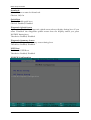
Configuration
This section allows users to configure further BIOS function.
Boot Configuration
NANO-5050 User’s Manual
4-3
BIOS Setup Information
NumLock:
Selects Power-on state for NumLock.
Choices: Off, On
Quick Boot
Enable/Disable quick boot.
Choices: Enabled, Disabled
Diagnostic Splash Screen
If you select ‘Enable’ the diagnostic splash screen always display during boot. If you
select ‘Disabled’ the diagnostic splash screen dose not display unless you press
HOTKEY during boot.
The choice: Enabled, Disabled.
Diagnostic Summary Screen
Display the Diagnostic summary screen during boot.
The choice: Enabled, Disabled.
UEFI Boot
Enables the UEFI Boot.
The choice: Enabled, Disabled.
PCI/PCIE Configuration
NANO-5050 User’s Manual
4-4
BIOS Setup Information
PCH PCI Express Configuration
DMI Link ASPM Control
The control of active state Power Management on both NB side of the DMI Link.
Choices: Enabled, Disabled.
PCI Express Root Port 1~4
NANO-5050 User’s Manual
4-5
BIOS Setup Information
PCI Express Root Port 1/2/3/4
Control the PCI Express Root Port.
PCIe Speed
Select PCIe Speed to Gen1 or Gen2 .
ASPM
Control PCIe Active State Power Management settings.
configure : Disable, L0S, L1, L0S And L1, Auto
HOT PLUG
Enable or disable PCI Express Hot Plug.
URR
Enable or disable PCI Express Unsupported Request Reporting.
FER
Enable or disable PCI Express Device Fatal Error Reporting.
NFER
Enable or disable PCI Express Device Non-Fatal Error Reporting.
CER
Enable or disable PCI Express Device Correctable Error Reporting.
SEFE
Enable or disable Root PCI Express System Error on Fatal Error.
SENFE
Root PCI Express System Error on Non-Fatal Error Enable/Disable.
SECE
Root PCI Express System Error on Correctable Error Enable/Disable.
PME Interrupt
Root PCI Express PME Interrupt Enable/Disable.
NANO-5050 User’s Manual
4-6
BIOS Setup Information
Power Control Configuration
ACPI Sleep State
Select the highest ACPI sleep state the system will enter when the SUSPEND button
is pressed.
The choice: S1 (CPU Stop Clock), S3 (Suspend to RAM)
Restore AC power loss
Select AC Power state when power is re-applied after a power failure.
The choice: Power Off, Power On, Last State.
The choice: Disabled, Enabled.
Wake System With Fixed Time
Enable or disable System wake on alarm event. When enabled, System will wake on
the hr::min::sec specified.
Choices: Enabled, Disabled.
Wake up By Ring
Enable or disable Ring to wake the system.
Choices: Enabled, Disabled.
NANO-5050 User’s Manual
4-7
BIOS Setup Information
CPU Configuration
Hyper-threading
Enabled for Windows XP and Linux (OS optimized for Hyper-Threading
Technology) and Disabled for other OS (OS not optimized for Hyper- Threading
Technology). When Disabled only one.
Choices: Enabled, Disabled.
Active Processor Cores
Select the number of physical cores to enable in each processor package.
Choices: 1, All.
Execute Disable Bit
Enable Execute Disabled functionality. Also known as Data Execution Prevention
(DEP).
Local x2APIC
Enable Local x2APIC. Some 0Ses do not support this.
Choices: Enabled, Disabled.
NANO-5050 User’s Manual
4-8
BIOS Setup Information
LAN Configuration
LAN Control
LAN Control Enabled/Disabled.
Choices: Enabled, Disabled.
Wake on LAN
Enable or disable integrated LAN to wake the system.
Choices: Enabled, Disabled.
LAN Boot ROM
Enable or disable integrated LAN Boot ROM(PXE) function.
Choices: Enabled, Disabled.
NANO-5050 User’s Manual
4-9
BIOS Setup Information
Chipset Configuration
VT-d
Check to enable VT-d function on MCH.
Choices: Enabled, Disabled.
Azalia
Control Detection of the Azalia device.
Choices: Enabled, Disabled.
NANO-5050 User’s Manual
4-10
BIOS Setup Information
NB PCIe Configuration
Always Enable PEG
To Enable the PEG Slot.
Choices: Enabled, Disabled.
PEG ASPM
Control ASPM Support for the PEG Device. This has mp effect if PEF is not the
current active device.
Choices: Disabled, Auto, ASPM L0s, ASPM L1, ASPM L0sL1.
NANO-5050 User’s Manual
4-11
BIOS Setup Information
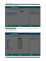
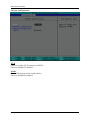
Memory Configuration
Graphic Configuration
NANO-5050 User’s Manual
4-12
BIOS Setup Information
Primary Display
Select which of IGFX/PEG/PCI Graphics device should be Primary Display or select
SG for Switchable Gfx.
The choice: Auto, IGFX, PEG.
Boot Display
Select the video Device which will be activated during POST. This has no effect if
external graphics present. Secondary boot display selection will appear based on
your selection. VGA modes will be supported only on primary display.
Choices: Auto, CRT, DP, LVDS, CRT+LVDS, CRT+DP, LVDS + DP
LVDS Panel Type
Select LCD Panel used by internal Graphics by selecting the appropriate setup item.
Choices: 800x600, 1024x768, 1280x800, 1280x1024, 1920x1080
Backlight Control
Choices: Level 1, Level 2, Level 3, Level 4, Level 5, Level 6, Level 7.
SATA Configuration
NANO-5050 User’s Manual
4-13
BIOS Setup Information
SATA Controller(s)
Determines how SATA controller(s) operate
Choices: Enabled, Disabled
Launch Storage OpROM
Enable or disable boot option Launch Storage devices with option ROM.
Choices: Enabled, Disabled.
SATA Mode
Determines how SATA controller(s) operate.
The choice: IDE, AHCI.
Serial ATA Port 0/1
Display the identity of the device attached.
USB Configuration
Legacy USB Support
Enable Legacy USB support. AUTO option disables legacy support if no USB devices
are connected. DISABLE option will keep USB device available only for EFI
applications
Choices: Enabled Disabled.
NANO-5050 User’s Manual
4-14
BIOS Setup Information
PCH USB Configuration
UHCI Controller #1~#3
Control each of the USB Controller(1~4)
Choices: Enabled, Disabled
CF-SATA Enable
CF-SATA Enable/Disable.
Choices: Enabled, Disabled.
NANO-5050 User’s Manual
4-15
BIOS Setup Information
SIO Configuration
NANO-5050 User’s Manual
4-16
BIOS Setup Information
Serial Port 1
Choices: 3F8/IRQ4, 2F8/IRQ3, Disable.
Mode
Choices: RS-232, RS-422, RS-485.
Watch Dog Timer Select
Choices: Disable, 15secs, 30secs, 1min, 2mins, 3mins
Hardware Monitor
SYS1 Target Temp:
SYS1 FAN Target Temperature
Choices: Disable, 40°C, 45°C, 50°C, 55°C.
SYS1 Tolerance Temp:
CPU FAN Tolerance Temperature
Choices: Disable, 5°C, 4°C, 3°C, 2°C, 1°C.
NANO-5050 User’s Manual
4-17
BIOS Setup Information
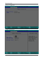
Serial Port Console Configuration
Console Redirection
Console Redirection Enable or Disable
Choices: Enabled, Disabled
NANO-5050 User’s Manual
4-18
BIOS Setup Information
Console Redirection Setting
Terminal Type
VT-UTF8 is the preferred terminal type for out-of-band management. The next best
choice is VT100+ and then VT100. See above, in console Redirection Settings page,
for more Help with Terminal Type/Emulation.
The choice: VT100, VT100+, VT-UTF8, ANSI
Bits Per second
Select serial port transmission speed
The choice: 9600, 19200, 57600, 115200.
NANO-5050 User’s Manual
4-19
BIOS Setup Information
4.4
Security
This section lets you set security passwords to control access to the system at boot
time and/or when entering the BIOS setup program. Some systems have a single
password, while many newer ones now have two: a supervisor and a user password.
Set Supervisor Password
Set or Clear Supervisor Password
Supervisor Hint String
Press Enter to type Supervisor Hint String
Min. password length
Set the minimum number of characters for password (1-20).
Flash Controller Lock
Lock all flash controllers
The choice: Enabled, Disabled.
NANO-5050 User’s Manual
4-20
BIOS Setup Information
4.5
Boot
Use this menu to specify the priority of boot devices.
1st Drive
This setting allows users to set the priority of the removable devices. First press
<Enter> to enter the sub-menu. Then you may use the arrow keys (↑↓) to select the
desired device, then press <+>, <-> or <PageUp>, <PageDown> key to move it
up/down in the priority list.
The choice: 1st FLOPPY DRICE, Disabled.
NANO-5050 User’s Manual
4-21
BIOS Setup Information
4.6
Exit
This menu allows you to load the BIOS default values or factory default settings into
the BIOS and exit the BIOS setup utility with or without changes.
Exit Saving Changes
Equal to F10, save all changes of all menus, then exit setup configure driver. Finally
resets the system automatically.
Exit Discarding Changes
Equal to ESC, never save changes, than exit setup configure driver.
Load Setup Defaults
Equal to F9. Load standard default values.
Discard Changes
Load the original value of this boot time. Not the default Setup value.
Save Changes
Save all changes of all menus, but do not reset system. options.
NANO-5050 User’s Manual
4-22
Troubleshooting
Chapter 5
Troubleshooting
This chapter provides a few useful tips to quickly get NANO-5050 running with
success. As basic hardware installation has been addressed in Chapter 2, this chapter
will be focusing on system integration issues, in terms of BIOS setting, and OS
diagnostics.
5.1
Hardware Quick Installation
There are two methods to connect the power of NANO-5050 which are 12V DC Jack
& 4 Pins 12V DC input. It’s able to be chosen either one for NANO-5050. Can be
referred as the picture shows blew.
4 Pin 12V DC input (J13)
12V DC Jack input (J1)
※ Please do not connect both power input at the same time!
NANO-5050 User’s Manual
5-1
Troubleshooting
Please also make sure every other necessary devices are connected before hooking
up power source.
Loading the default optimal setting
When prompted with the main setup menu, please scroll down to “Load Setup
Defaults”, press “Enter” and “Y” to load in default optimal BIOS setup. This will
force your BIOS setting back to the initial factory configuration. It is recommended
to do this so you can be sure the system is running with the BIOS setting that
Portwell has highly endorsed. As a matter of fact, users can load the default BIOS
setting any time when system appears to be unstable in boot up sequence.
5.2
FQA
Question: I forget my password of system BIOS, what am I supposed to do?
Answer: You can simply short 2-3 pins on J14 to clean your password.
Question: I cannot boot up my system!
Answer: Please make sure all the setups were followed the instruction in User’s
manual. Unplugged any other add-on device to isolate the possibility of external
affection and try again. If the SBC still does not boot, please contact with our
Technical support department.
Note:
Please visit our technical web site at http://www.portwell.com.tw
For additional technical information, which is not covered in this manual, you can
mail to [email protected] or you can also send mail to our sales, they will be very
delighted to forward them to us.
NANO-5050 User’s Manual
5-2
Troubleshooting
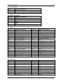
System Memory Address Map
Each On-board device in the system is assigned a set of memory addresses, which
also can be identical of the device. The following table lists the system memory
address used for your reference.
System Memory Address Map
Memory Area
0000-003F
0040-004F
0050-006F
0070-0E2E
0E2F-0F6B
0F6C-9B7F
9B80-9D7F
First Meg
9D80-9DFF
9E00-9FFF
A000-AFFF
B000-B7FF
B800-BFFF
C000-CF3F
CF40-EFFF
F000-FFFF
HMA
NANO-5050 User’s Manual
Size
1K
0.3 K
0.5 K
54 K
5K
560 K
8K
Description
Interrupt Area
BIOS Data Area
System Data
DOS
Program Area
【Available】
Unused
-- Conventional memory end at 630K -2K
Extended BIOS Area
8K
Unused
64 K
VGA Graphics
32 K
Unused
32 K
VGA Text
61 K
Video ROM
131 K
Unused
64 K
System ROM
64 K
First 64K Extended
5-3
Troubleshooting
Interrupt Request Lines (IRQ)
IRQ#
IRQ 0
IRQ 1
IRQ 2
IRQ 3
IRQ 4
IRQ 5
IRQ 6
IRQ 7
IRQ 8
IRQ 9
IRQ 10
IRQ 11
IRQ 12
IRQ 13
IRQ 14
IRQ 15
NANO-5050 User’s Manual
Interrupt Request Lines IRQ
Current Use
Unused
System ROM
【Unassigned】
System ROM
System ROM
【Unassigned】
System ROM
Unused
System ROM
【Unassigned】
【Unassigned】
【Unassigned】
System ROM
System ROM
System ROM
【Unassigned】
Default Use
System Timer
Keyboard Event
Usable IRQ
COM2
COM1
Usable IRQ
Diskette Event
Usable IRQ
Real-Time Clock
Usable IRQ
Usable IRQ
Usable IRQ
IBM Mouse Event
Coprocessor Error
Hard Disk Event
Usable IRQ
5-4