1
UM1724
User manual
STM32 Nucleo-64 boards
Introduction
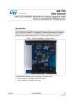
The STM32 Nucleo-64 board (NUCLEO-F030R8, NUCLEO-F070RB, NUCLEO-F072RB,
NUCLEO-F091RC, NUCLEO-F103RB, NUCLEO-F302R8, NUCLEO-F303RE,
NUCLEO-F334R8, NUCLEO-F401RE, NUCLEO-F410RB, NUCLEO-F411RE,
NUCLEO-F446RE, NUCLEO-L053R8, NUCLEO-L073RZ, NUCLEO-L152RE,
NUCLEO-L476RG) provides an affordable and flexible way for users to try out new ideas
and build prototypes with the STM32 microcontrollers in LQFP64 package, choosing from
the various combinations of performance, power consumption and features. The Arduino™
connectivity support and ST Morpho headers make it easy to expand the functionality of the
Nucleo open development platform with a wide choice of specialized shields. The STM32
Nucleo board does not require any separate probe as it integrates the ST-LINK/V2-1
debugger/programmer. The STM32 Nucleo board comes with the STM32 comprehensive
software HAL library together with various packaged software examples, as well as direct
access to mbed online resources at http://mbed.org/.
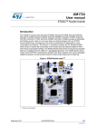
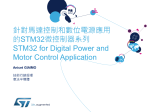
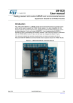
Figure 1. STM32 Nucleo-64 board (1)
1. Picture not contractual.
July 2015
DocID025833 Rev 8
1/62
www.st.com
1
Content
UM1724
Content
1
Ordering information . . . . . . . . . . . . . . . . . . . . . . . . . . . . . . . . . . . . . . . . 2
2
Conventions . . . . . . . . . . . . . . . . . . . . . . . . . . . . . . . . . . . . . . . . . . . . . . . 3
3
Quick start . . . . . . . . . . . . . . . . . . . . . . . . . . . . . . . . . . . . . . . . . . . . . . . . . 4
4
3.1
Getting started . . . . . . . . . . . . . . . . . . . . . . . . . . . . . . . . . . . . . . . . . . . . . . 4
3.2
System requirements . . . . . . . . . . . . . . . . . . . . . . . . . . . . . . . . . . . . . . . . . 4
Features . . . . . . . . . . . . . . . . . . . . . . . . . . . . . . . . . . . . . . . . . . . . . . . . . . . 5
4.1
5
Hardware layout and configuration . . . . . . . . . . . . . . . . . . . . . . . . . . . . . 6
5.1
Cuttable PCB . . . . . . . . . . . . . . . . . . . . . . . . . . . . . . . . . . . . . . . . . . . . . . . 8
5.2
Embedded ST-LINK/V2-1 . . . . . . . . . . . . . . . . . . . . . . . . . . . . . . . . . . . . . . 9
5.3
1/62
Hardware configuration variants . . . . . . . . . . . . . . . . . . . . . . . . . . . . . . . . . 5
5.2.1
Driver
. . . . . . . . . . . . . . . . . . . . . . . . . . . . . . . . . . . . . . . . . . . . . . . . . . 10
5.2.2
ST-LINK/V2-1 firmware upgrade . . . . . . . . . . . . . . . . . . . . . . . . . . . . . . 10
5.2.3
Using the ST-LINK/V2-1 to program/debug the STM32 on board
5.2.4
Using ST-LINK/V2-1 to program/debug an external STM32 application 11
. . . . 11
Power supply and power selection . . . . . . . . . . . . . . . . . . . . . . . . . . . . . . 12
5.3.1
Power supply input from the USB connector . . . . . . . . . . . . . . . . . . . . . 12
5.3.2
External power supply inputs: VIN and EV5 . . . . . . . . . . . . . . . . . . . . . 13
5.3.3
External power supply input: + 3V3 . . . . . . . . . . . . . . . . . . . . . . . . . . . . 16
5.3.4
External power supply output . . . . . . . . . . . . . . . . . . . . . . . . . . . . . . . . 16
5.4
LEDs . . . . . . . . . . . . . . . . . . . . . . . . . . . . . . . . . . . . . . . . . . . . . . . . . . . . 16
5.5
Push buttons . . . . . . . . . . . . . . . . . . . . . . . . . . . . . . . . . . . . . . . . . . . . . . 17
5.6
JP6 (IDD) . . . . . . . . . . . . . . . . . . . . . . . . . . . . . . . . . . . . . . . . . . . . . . . . . 17
5.6.1
OSC clock supply . . . . . . . . . . . . . . . . . . . . . . . . . . . . . . . . . . . . . . . . . 17
5.6.2
OSC 32 kHz clock supply . . . . . . . . . . . . . . . . . . . . . . . . . . . . . . . . . . . 18
5.7
USART communication . . . . . . . . . . . . . . . . . . . . . . . . . . . . . . . . . . . . . . 19
5.8
Solder bridges . . . . . . . . . . . . . . . . . . . . . . . . . . . . . . . . . . . . . . . . . . . . . 19
5.9
Extension connectors . . . . . . . . . . . . . . . . . . . . . . . . . . . . . . . . . . . . . . . . 21
5.10
Arduino connectors . . . . . . . . . . . . . . . . . . . . . . . . . . . . . . . . . . . . . . . . . 29
5.11
STMicroelectronics Morpho connector . . . . . . . . . . . . . . . . . . . . . . . . . . . 45
DocID025833 Rev 8
UM1724
Content
6
Mechanical drawing . . . . . . . . . . . . . . . . . . . . . . . . . . . . . . . . . . . . . . . . 54
7
Electrical schematics . . . . . . . . . . . . . . . . . . . . . . . . . . . . . . . . . . . . . . . 55
8
References . . . . . . . . . . . . . . . . . . . . . . . . . . . . . . . . . . . . . . . . . . . . . . . . 59
9
Revision history . . . . . . . . . . . . . . . . . . . . . . . . . . . . . . . . . . . . . . . . . . . 60
DocID025833 Rev 8
2/62
2
List of Tables
UM1724
List of Tables
Table 1.
Table 2.
Table 3.
Table 4.
Table 5.
Table 6.
Table 7.
Table 8.
Table 9.
Table 10.
Table 11.
Table 12.
Table 13.
Table 14.
Table 15.
Table 16.
Table 17.
Table 18.
Table 19.
Table 20.
Table 21.
Table 22.
Table 23.
Table 24.
Table 25.
Table 26.
Table 27.
Table 28.
Table 29.
Table 30.
Table 31.
1/62
Ordering information . . . . . . . . . . . . . . . . . . . . . . . . . . . . . . . . . . . . . . . . . . . . . . . . . . . . . . . 2
ON/OFF conventions . . . . . . . . . . . . . . . . . . . . . . . . . . . . . . . . . . . . . . . . . . . . . . . . . . . . . . 3
Jumper states . . . . . . . . . . . . . . . . . . . . . . . . . . . . . . . . . . . . . . . . . . . . . . . . . . . . . . . . . . . . 9
Debug connector CN4 (SWD) . . . . . . . . . . . . . . . . . . . . . . . . . . . . . . . . . . . . . . . . . . . . . . 11
JP1 configuration table . . . . . . . . . . . . . . . . . . . . . . . . . . . . . . . . . . . . . . . . . . . . . . . . . . . . 13
External power sources . . . . . . . . . . . . . . . . . . . . . . . . . . . . . . . . . . . . . . . . . . . . . . . . . . . 14
Power-related jumper . . . . . . . . . . . . . . . . . . . . . . . . . . . . . . . . . . . . . . . . . . . . . . . . . . . . . 14
+3.3V eternal power source . . . . . . . . . . . . . . . . . . . . . . . . . . . . . . . . . . . . . . . . . . . . . . . . 16
Solder bridges. . . . . . . . . . . . . . . . . . . . . . . . . . . . . . . . . . . . . . . . . . . . . . . . . . . . . . . . . . . 19
Arduino connectors on
NUCLEO-F030R8, NUCLEO-F070RB, NUCLEO-F072RB, NUCLEO-F091RC. . . . . . . . . 29
Arduino connectors on NUCLEO-F103RB . . . . . . . . . . . . . . . . . . . . . . . . . . . . . . . . . . . . . 30
Arduino connectors on NUCLEO-F302R8 . . . . . . . . . . . . . . . . . . . . . . . . . . . . . . . . . . . . . 32
Arduino connectors on NUCLEO-F303RE . . . . . . . . . . . . . . . . . . . . . . . . . . . . . . . . . . . . . 34
Arduino connectors on NUCLEO-F334R8 . . . . . . . . . . . . . . . . . . . . . . . . . . . . . . . . . . . . . 35
Arduino connectors on NUCLEO-F401RE, NUCLEO-F411RE . . . . . . . . . . . . . . . . . . . . . 36
Arduino connectors on NUCLEO-L053R8 . . . . . . . . . . . . . . . . . . . . . . . . . . . . . . . . . . . . . 37
Arduino connectors on NUCLEO-L073RZ . . . . . . . . . . . . . . . . . . . . . . . . . . . . . . . . . . . . . 39
Arduino connectors on NUCLEO-F446RE . . . . . . . . . . . . . . . . . . . . . . . . . . . . . . . . . . . . . 41
Arduino connectors on NUCLEO-F410RB . . . . . . . . . . . . . . . . . . . . . . . . . . . . . . . . . . . . . 42
Arduino connectors on NUCLEO-L152RE . . . . . . . . . . . . . . . . . . . . . . . . . . . . . . . . . . . . . 43
Arduino connectors on NUCLEO-L476RG . . . . . . . . . . . . . . . . . . . . . . . . . . . . . . . . . . . . . 44
STMicroelectronics Morpho connector on NUCLEO-F030R8 . . . . . . . . . . . . . . . . . . . . . . 45
STMicroelectronics Morpho connector on NUCLEO-F070RB . . . . . . . . . . . . . . . . . . . . . . 46
STMicroelectronics Morpho connector on
NUCLEO-F072RB, NUCLEO-F091RC, NUCLEO-F303RE, NUCLEO-F334R8. . . . . . . . . 47
STMicroelectronics Morpho connector on NUCLEO-F103RB . . . . . . . . . . . . . . . . . . . . . . 48
STMicroelectronics Morpho connector on NUCLEO-F302R8 . . . . . . . . . . . . . . . . . . . . . . 49
STMicroelectronics Morpho connector on NUCLEO-F401RE,
NUCLEO-F411RE,NUCLEO-F446RE . . . . . . . . . . . . . . . . . . . . . . . . . . . . . . . . . . . . . . . . 50
STMicroelectronics Morpho connector on
NUCLEO-L053R8, NUCLEO-L073RZ, NUCLEO-L152RE . . . . . . . . . . . . . . . . . . . . . . . . . 51
STMicroelectronics Morpho connector on NUCLEO-L476RG . . . . . . . . . . . . . . . . . . . . . . 52
STMicroelectronics Morpho connector on NUCLEO-F410RB . . . . . . . . . . . . . . . . . . . . . . 53
Document revision history . . . . . . . . . . . . . . . . . . . . . . . . . . . . . . . . . . . . . . . . . . . . . . . . . 60
DocID025833 Rev 8
UM1724
List of Figures
List of Figures
Figure 1.
Figure 1.
Figure 2.
Figure 3.
Figure 4.
Figure 5.
Figure 6.
Figure 7.
Figure 8.
Figure 9.
Figure 10.
Figure 11.
Figure 12.
Figure 13.
Figure 14.
Figure 15.
Figure 16.
Figure 17.
Figure 18.
Figure 19.
Figure 20.
Figure 21.
Figure 22.
Figure 23.
Figure 24.
Figure 25.
Figure 26.
Figure 27.
Figure 28.
STM32 Nucleo-64 board (1) . . . . . . . . . . . . . . . . . . . . . . . . . . . . . . . . . . . . . . . . . . . . . . . . . 1
Hardware block diagram . . . . . . . . . . . . . . . . . . . . . . . . . . . . . . . . . . . . . . . . . . . . . . . . . . . 6
Top layout . . . . . . . . . . . . . . . . . . . . . . . . . . . . . . . . . . . . . . . . . . . . . . . . . . . . . . . . . . . . . . . 7
Bottom layout . . . . . . . . . . . . . . . . . . . . . . . . . . . . . . . . . . . . . . . . . . . . . . . . . . . . . . . . . . . . 8
Typical configuration . . . . . . . . . . . . . . . . . . . . . . . . . . . . . . . . . . . . . . . . . . . . . . . . . . . . . . 10
Updating the list of drivers in Device Manager . . . . . . . . . . . . . . . . . . . . . . . . . . . . . . . . . . 10
Connecting the STM32 Nucleo board to program the on-board STM32 . . . . . . . . . . . . . . 11
Using ST-LINK/V2-1 to program the STM32 on an external application . . . . . . . . . . . . . . 12
NUCLEO-F030R8 . . . . . . . . . . . . . . . . . . . . . . . . . . . . . . . . . . . . . . . . . . . . . . . . . . . . . . . . 21
NUCLEO-F070RB . . . . . . . . . . . . . . . . . . . . . . . . . . . . . . . . . . . . . . . . . . . . . . . . . . . . . . . 21
NUCLEO-F072RB . . . . . . . . . . . . . . . . . . . . . . . . . . . . . . . . . . . . . . . . . . . . . . . . . . . . . . . 22
NUCLEO-F091RC . . . . . . . . . . . . . . . . . . . . . . . . . . . . . . . . . . . . . . . . . . . . . . . . . . . . . . . 22
NUCLEO-F103RB . . . . . . . . . . . . . . . . . . . . . . . . . . . . . . . . . . . . . . . . . . . . . . . . . . . . . . . 23
NUCLEO-F302R8 . . . . . . . . . . . . . . . . . . . . . . . . . . . . . . . . . . . . . . . . . . . . . . . . . . . . . . . . 23
NUCLEO-F303RE . . . . . . . . . . . . . . . . . . . . . . . . . . . . . . . . . . . . . . . . . . . . . . . . . . . . . . . 24
NUCLEO-F334R8 . . . . . . . . . . . . . . . . . . . . . . . . . . . . . . . . . . . . . . . . . . . . . . . . . . . . . . . . 24
NUCLEO-F401RE . . . . . . . . . . . . . . . . . . . . . . . . . . . . . . . . . . . . . . . . . . . . . . . . . . . . . . . 25
NUCLEO-F411RE . . . . . . . . . . . . . . . . . . . . . . . . . . . . . . . . . . . . . . . . . . . . . . . . . . . . . . . 25
NUCLEO-L053R8 . . . . . . . . . . . . . . . . . . . . . . . . . . . . . . . . . . . . . . . . . . . . . . . . . . . . . . . . 26
NUCLEO-L073RZ . . . . . . . . . . . . . . . . . . . . . . . . . . . . . . . . . . . . . . . . . . . . . . . . . . . . . . . . 26
NUCLEO-L152RE. . . . . . . . . . . . . . . . . . . . . . . . . . . . . . . . . . . . . . . . . . . . . . . . . . . . . . . . 27
NUCLEO-L476RG . . . . . . . . . . . . . . . . . . . . . . . . . . . . . . . . . . . . . . . . . . . . . . . . . . . . . . . 27
NUCLEO-F446RE . . . . . . . . . . . . . . . . . . . . . . . . . . . . . . . . . . . . . . . . . . . . . . . . . . . . . . . 28
NUCLEO-F410RB . . . . . . . . . . . . . . . . . . . . . . . . . . . . . . . . . . . . . . . . . . . . . . . . . . . . . . . 28
STM32 Nucleo board mechanical drawing . . . . . . . . . . . . . . . . . . . . . . . . . . . . . . . . . . . . . 54
Electrical schematics (1/4) . . . . . . . . . . . . . . . . . . . . . . . . . . . . . . . . . . . . . . . . . . . . . . . . . 55
Electrical schematics (2/4) . . . . . . . . . . . . . . . . . . . . . . . . . . . . . . . . . . . . . . . . . . . . . . . . . 56
Electrical schematics (3/4) . . . . . . . . . . . . . . . . . . . . . . . . . . . . . . . . . . . . . . . . . . . . . . . . . 57
Electrical schematics (4/4) . . . . . . . . . . . . . . . . . . . . . . . . . . . . . . . . . . . . . . . . . . . . . . . . . 58
DocID025833 Rev 8
1/62
1
Ordering information
1
UM1724
Ordering information
Table 1 lists the order codes and the respective targeted MCU.
Table 1. Ordering information
Order code
Targeted MCU
NUCLEO-F030R8
STM32F030R8T6
NUCLEO-F070RB
STM32F070RBT6
NUCLEO-F072RB
STM32F072RBT6
NUCLEO-F091RC
STM32F091RCT6
NUCLEO-F103RB
STM32F103RBT6
NUCLEO-F302R8
STM32F302R8T6
NUCLEO-F303RE
STM32F303RET6
NUCLEO-F334R8
STM32F334R8T6
NUCLEO-F401RE
STM32F401RET6
NUCLEO-F410RB
STM32F410RBT6
NUCLEO-F411RE
STM32F411RET6
NUCLEO-F446RE
STM32F446RET6
NUCLEO-L053R8
STM32L053R8T6
NUCLEO-L073RZ
STM32L073RZT6
NUCLEO-L152RE
STM32L152RET6
NUCLEO-L476RG
STM32L476RGT6
The meaning of NUCLEO-TXXXRY codification is as follows:
TXXX describes the STM32 MCU product line
R describes the pin count (R for 64 pins)
Y describes the code size (8 for 64K, B for 128K, C for 256K, E for 512K, G for 1MB, Z
for 192K)
The order code is printed on a sticker placed at the top or bottom side of the board.
2/62
DocID025833 Rev 8
UM1724
2
Conventions
Conventions
Table 2 provides the conventions used for the ON and OFF settings in the present
document.
Table 2. ON/OFF conventions
Convention
Definition
Jumper JP1 ON
Jumper fitted
Jumper JP1 OFF
Jumper not fitted
Solder bridge SBx ON
SBx connections closed by solder or 0 ohm resistor
Solder bridge SBx OFF
SBx connections left open
We refer to “STM32 Nucleo board” and “STM32 Nucleo boards” in this document for all
information that is common to all sale types.
DocID025833 Rev 8
3/62
61
Quick start
3
UM1724
Quick start
The STM32 Nucleo board is a low-cost and easy-to-use development platform used to
quickly evaluate and start a development with an STM32 microcontroller in LQFP64
package.
Before installing and using the product, please accept the Evaluation Product License
Agreement from www.st.com/epla.
For more information on the STM32 Nucleo boards and to access the demonstration
software, visit www.st.com/stm32nucleo.
3.1
Getting started
Follow the sequence below to configure the STM32 Nucleo board and launch the demo
software:
3.2
4/62
1.
Check the jumper position on the board, JP1 off, JP5 (PWR) on U5V, JP6 on (IDD),
CN2 on (NUCLEO) selected.
2.
For correct identification of all device interfaces from the host PC, install the Nucleo
USB driver available on www.st.com/stm32nucleo, prior to connecting the board
3.
Connect the STM32 Nucleo board to a PC with a USB cable ‘type A to mini-B’ through
USB connector CN1 to power the board. The red LED LD3 (PWR) and LD1 (COM)
should light up. LD1 (COM) and green LED LD2 should blink.
4.
Press button B1 (left button).
5.
Observe how the blinking of the green LED LD2 changes according to clicks on button
B1.
6.
The demo software and several software examples on how use the STM32 Nucleo
board features are available on www.st.com/stm32nucleo.
7.
Develop the application using the available examples.
System requirements
Windows OS (XP, 7, 8)
USB type A to Mini-B USB cable
DocID025833 Rev 8
UM1724
4
Features
Features
The STM32 Nucleo boards offer the following features:
STM32 microcontroller with LQFP64 package
Two types of extension resources
– Arduino Uno Revision 3 connectivity
– STMicroelectronics Morpho extension pin headers for full access to all STM32 I/Os
mbed-enabled(a)
On-board ST-LINK/V2-1 debugger/programmer with SWD connector
– selection-mode switch to use the kit as a standalone ST-LINK/V2-1
Flexible board power supply
–
USB VBUS
–
External VIN (7V<VIN<12V) supply voltage from Arduino connectors or ST
Morpho connector
–
External 5V (E5V) supply voltage from ST Morpho connector
–
External +3.3V supply voltage from Arduino connector or ST Morpho connector
Three LEDs
– USB communication (LD1), user LED (LD2), power LED (LD3)
Two push buttons: USER and RESET
LSE crystal:
– 32.768kHz crystal oscillator (depending on board version)
USB re-enumeration capability: three different interfaces supported on USB
– Virtual Com port
– Mass storage
– Debug port
Comprehensive free software HAL library including a variety of software examples
Supported by wide choice of Integrated Development Environments (IDEs) including IAR,
Keil, GCC-based IDEs
4.1
Hardware configuration variants
The board can be delivered with different configurations of the oscillator of the target MCU.
For all the details concerning High Speed oscillator configurations refer to Section 5.6.1. For
all the details concerning Low speed oscillator configurations refer to Section 5.6.2.
a. See http://mbed.org/
DocID025833 Rev 8
5/62
61
Hardware layout and configuration
5
UM1724
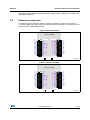
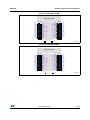
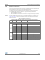
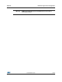
Hardware layout and configuration
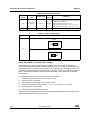
The STM32 Nucleo board is designed around the STM32 microcontrollers in a 64-pin LQFP
package.
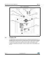
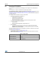
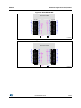
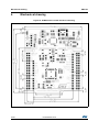
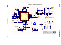
Figure 1 shows the connections between the STM32 and its peripherals (ST-LINK/V2-1,
pushbutton, LED, Arduino connectors and STMicroelectronics Morpho connector).
Figure 2 and Figure 3 show the location of these features on the STM32 Nucleo board.
Figure 1. Hardware block diagram
67/,1.SDUW
0LQL
86%
(PEHGGHG
67/,1.9
,2
670
0LFURFRQWUROOHU
,2
,2
5(6(7
,2
%
5(6(7
/('
/'
0RUSKRH[WHQVLRQKHDGHU
$UGXLQRFRQQHFWRU
0RUSKRH[WHQVLRQKHDGHU
%
86(5
$UGXLQRFRQQHFWRU
6:'
0&8SDUW
069
6/62
DocID025833 Rev 8
UM1724
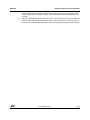
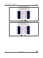
Hardware layout and configuration
Figure 2. Top layout
&1
67/,1.1XFOHR
VHOHFWRU
&1
6:'FRQQHFWRU
&1
67/,1.86%
PLQL%FRQQHFWRU
/'
5HG*UHHQ/('
&20
%
5(6(7EXWWRQ
%86(5
EXWWRQ
-3,''
PHDVXUHPHQW
6%
9UHJXODWRURXWSXW
/'
5HG/('
SRZHU
/'
*UHHQ/('
&1
$UGXLQR
FRQQHFWRU
&1
$UGXLQRFRQQHFWRU
&1
670RUSKR
FRQQHFWRU
&1
$UGXLQR
FRQQHFWRU
&1
670RUSKRFRQQHFWRU
&1
$UGXLQRFRQQHFWRU
.+]
FU\VWDO
8 670
PLFURFRQWUROOHU 069
1. Crystal may be present or not depending on board version, refer to Section 5.6.2
DocID025833 Rev 8
7/62
61
Hardware layout and configuration
UM1724
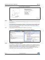
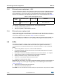
Figure 3. Bottom layout
4#4#
45-*/,64"35
4#4#4#4#
3&4&37&%
4#4#4#4#
%&'"6-5
4#
45-*/,480
6%
67/,1.
5(6(7
4#
45-*/,.$0
6%
86(5EXWWRQ
6%
86(5/('
6%
67/,1.0&2
.47
5.1
Cuttable PCB
The STM32 Nucleo board is divided into two parts: ST-LINK part and target MCU part. The
ST-LINK part of the PCB can be cut out to reduce the board size. In this case the remaining
target MCU part can only be powered by VIN, E5V and 3.3V on STMicroelectronics Morpho
connector CN7 or VIN and 3.3V on Arduino connector CN6. It is still possible to use the
ST-LINK part to program the main MCU using wires between CN4 and SWD signals
available on STMicroelectronics Morpho connector (SWCLK CN7 pin 15 and SWDIO CN7
pin 13).
8/62
DocID025833 Rev 8
UM1724
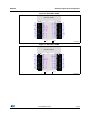
5.2
Hardware layout and configuration
Embedded ST-LINK/V2-1
The ST-LINK/V2-1 programming and debugging tool is integrated in the STM32 Nucleo
boards.
The ST-LINK/V2-1 makes the STM32 Nucleo boards mbed enabled.
The embedded ST-LINK/V2-1 supports only SWD for STM32 devices. For information about
debugging and programming features refer to UM1075 - ST-LINK/V2 in-circuit
debugger/programmer for STM8 and STM32, User manual, which describes in detail all the
ST-LINK/V2 features.
The changes versus ST-LINK/V2 version are listed below.
New features supported on ST-LINK/V2-1:
–
USB software re-enumeration
–
Virtual com port interface on USB
–
Mass storage interface on USB
–
USB power management request for more than 100 mA power on USB
Features not supported on ST-LINK/V2-1:
–
SWIM interface
–
Minimum supported application voltage limited to 3 V
Known limitation:
–
Activating the readout protection on ST-Link/V2-1 target prevents the target
application from running afterwards. The target readout protection must be kept
disabled on ST-Link/V2-1 boards.
There are two different ways to use the embedded ST-LINK/V2-1 depending on the jumper
states (see Table 3 and Figure 4):
Program/debug the MCU on board (Section 5.2.2),
Program/debug an MCU in an external application board using a cable connected to
SWD connector CN4 (Section 5.2.4).
Table 3. Jumper states
Jumper state
Description
Both CN2 jumpers ON
ST-LINK/V2-1 functions enabled for on board programming
(default)
Both CN2 jumpers OFF
ST-LINK/V2-1 functions enabled for external CN4 connector
(SWD supported)
DocID025833 Rev 8
9/62
61
Hardware layout and configuration
UM1724
Figure 4. Typical configuration
+DUGZDUHUHTXLUHPHQWV
86%FDEOHW\SH$WRPLQL%
FRPSXWHUZLWK:LQGRZV;3
'HYHORSPHQWWRROFKDLQ
,$5(:$50
.HLO0'.$50
*&&EDVHG,'(
069
5.2.1
Driver
The ST-LINK/V2-1 requires a dedicated USB driver, which can be found on www.st.com for
Windows XP, 7, 8.
In case the STM32 Nucleo board is connected to the PC before the driver is installed, some
Nucleo interfaces may be declared as “Unknown” in the PC device manager. In this case
the user must install the driver files (Figure 5), and from the device manager update the
driver of the connected device.
Note:
Prefer using the “USB Composite Device” handle for a full recovery.
Figure 5. Updating the list of drivers in Device Manager
5.2.2
ST-LINK/V2-1 firmware upgrade
The ST-LINK/V2-1 embeds a firmware upgrade mechanism for in-situ upgrade through the
USB port. As the firmware may evolve during the life time of the ST-LINK/V2-1 product (for
example new functionality, bug fixes, support for new microcontroller families), it is
recommended to visit www.st.com before starting to use the STM32 Nucleo board and
periodically, in order to stay up-to-date with the latest firmware version.
10/62
DocID025833 Rev 8
UM1724
5.2.3
Hardware layout and configuration
Using the ST-LINK/V2-1 to program/debug the STM32 on board
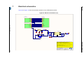
To program the STM32 on the board, plug in the two jumpers on CN2, as shown in red in
Figure 6. Do not use the CN4 connector as this could disturb the communication with the
STM32 microcontroller of the STM32 Nucleo board.
Figure 6. Connecting the STM32 Nucleo board to program the on-board STM32
EϮũƵŵƉĞƌƐKE
Eϰ^t
ĐŽŶŶĞĐƚŽƌ
069
5.2.4
Using ST-LINK/V2-1 to program/debug an external STM32 application
It is very easy to use the ST-LINK/V2-1 to program the STM32 on an external application.
Simply remove the two jumpers from CN2 as illustrated in Figure 7, and connect the
application to the CN4 debug connector according to Table 4.
Note:
SB12 NRST (target MCU RESET) must be OFF if CN4 pin 5 is used in the external
application.
Table 4. Debug connector CN4 (SWD)
Pin
CN4
Designation
1
VDD_TARGET
VDD from application
2
SWCLK
SWD clock
3
GND
Ground
4
SWDIO
SWD data input/output
DocID025833 Rev 8
11/62
61
Hardware layout and configuration
UM1724
Table 4. Debug connector CN4 (SWD) (continued)
5
NRST
RESET of target MCU
6
SWO
Reserved
Figure 7. Using ST-LINK/V2-1 to program the STM32 on an external application
$/KVNQFST0''
$/
48%DPOOFDUPS
.47
5.3
Power supply and power selection
The power supply is provided either by the host PC through the USB cable, or by an
external Source: VIN (7V-12V), E5V (5V) or +3V3 power supply pins on CN6 or CN7. In
case VIN, E5V or +3V3 is used to power the Nucleo board, using an external power supply
unit or an auxiliary equipment, this power source must comply with the standard EN-609501: 2006+A11/2009, and must be Safety Extra Low Voltage (SELV) with limited power
capability.
5.3.1
Power supply input from the USB connector
The ST-LINK/V2-1 supports USB power management allowing to request more than
100 mA current to the host PC.
12/62
DocID025833 Rev 8
UM1724
Hardware layout and configuration
All parts of the STM32 Nucleo board and shield can be powered from the ST-LINK USB
connector CN1 (U5V or VBUS). Note that only the ST-LINK part is power supplied before
the USB enumeration as the host PC only provides 100 mA to the board at that time. During
the USB enumeration, the STM32 Nucleo board requires 300 mA of current to the Host PC.
If the host is able to provide the required power, the targeted STM32 microcontroller is
powered and the red LED LD3 is turned ON, thus the STM32 Nucleo board and its shield
can consume a maximum of 300 mA current, not more. If the host is not able to provide the
required current, the targeted STM32 microcontroller and the MCU part including the
extension board are not power supplied. As a consequence the red LED LD3 remains
turned OFF. In such case it is mandatory to use an external power supply as explained in
the next chapter.
When the board is power supplied by USB (U5V) a jumper must be connected between pin
1 and pin 2 of JP5 as shown in Table 7.
JP1 is configured according to the maximum current consumption of the board when
powered by USB (U5V). JP1 jumper can be set in case the board is powered by USB and
maximum current consumption on U5V doesn’t exceed 100mA (including an eventual
extension board or Arduino Shield). In such condition USB enumeration will always succeed
since no more than 100mA is requested to the PC. Possible configurations of JP1 are
summarized in Table 5.
Table 5. JP1 configuration table
Jumper state
JP1 jumper OFF
JP1 jumper ON
Warning:
Power supply
USB power through CN1
Allowed current
300 mA max
100 mA max
If the maximum current consumption of the NUCLEO and its
extension boards exceeds 300 mA, it is mandatory to power
the NUCLEO using an external power supply connected to
E5V or VIN.
Note:
In case the board is powered by an USB charger, there is no USB enumeration, so the led
LD3 remains set to OFF permanently and the target MCU is not powered. In this specific
case the jumper JP1 needs to be set to ON, to allow target MCU to be powered anyway.
5.3.2
External power supply inputs: VIN and EV5
The external power sources VIN and EV5 are summarized in the Table 6. When the board is
power supplied by VIN or E5V, the jumpers configuration must be the following:
Jumper on JP5 pin 2 and pin 3
Jumper removed on JP1
DocID025833 Rev 8
13/62
61
Hardware layout and configuration
UM1724
Table 6. External power sources
Input power Connectors
Voltage range
name
pins
Max
current
Limitation
VIN
CN6 pin 8
CN7 pin 24
7 V to 12 V
800 mA
From 7 V to 12 V only and input current capability
is linked to input voltage:
800 mA input current when Vin=7 V
450 mA input current when 7 V<Vin (< or =) 9 V
250 mA input current when 9 V<Vin (< or =) 12 V
E5V
CN7 pin 6
4.75 V to 5.25 V
500 mA
-
Table 7. Power-related jumper
Jumper
Description
(9
89
U5V (ST-LINK VBUS) is used as power source when JP5 is set as shown below (Default
setting)
89
VIN or E5V is used as power source when JP5 is set as shown below.
(9
JP5
Using VIN or E5V as external power supply
VIN or E5V can be used as external power supply in case the current consumption of
NUCLEO and extensions boards exceeds the allowed current on USB. In this condition it is
still possible to use the USB for communication, for programming or debugging only, but it is
mandatory to power supply the board first using VIN or E5V then connect the USB cable to
the PC. Proceeding this way ensures that the enumeration occurs thanks to the external
power source.
The following power sequence procedure must be respected:
1.
Connect the jumper between pin 2 and pin 3 of JP5.
2.
Check that JP1 is removed.
3.
Connect the external power source to VIN or E5V.
4.
Power on the external power supply 7 V< VIN < 12 V to VIN, or 5 V for E5V.
5.
Check that LD3 is turned ON.
6.
Connect the PC to USB connector CN1.
If this order is not respected, the board may be supplied by VBUS first then by VIN or E5V,
and the following risks may be encountered:
14/62
DocID025833 Rev 8
UM1724
Hardware layout and configuration
1.
If more than 300 mA current is needed by the board, the PC may be damaged or the
current supply can be limited by the PC. As a consequence the board is not powered
correctly.
2.
300 mA is requested at enumeration (since JP1 must be OFF) so there is risk that the
request is rejected and the enumeration does not succeed if the PC cannot provide
such current. Consequently the board is not power supplied (LED LD3 remains OFF).
DocID025833 Rev 8
15/62
61
Hardware layout and configuration
5.3.3
UM1724
External power supply input: + 3V3
It can be of interest to use the +3V3 (CN6 pin 4 or CN7 pin 12 and pin 16) directly as power
input for instance in case the 3.3 V is provided by an extension board. When NUCLEO is
power supplied by +3V3, the ST-LINK is not powered thus the programming and debug
features are unavailable. The external power sources +3.3V is summarized in the Table 8.
Table 8. +3.3V eternal power source
Input power
name
Connectors pins
Voltage range
Limitation
+3V3
CN6 pin 4
CN7 pin 12 and pin 16
3 V to 3.6 V
Used when ST-LINK part of PCB is cut or
SB2 and SB12 OFF
Two different configurations are possible to use +3V3 to power the board:
5.3.4
ST-LINK is removed (PCB cut), or
SB2 (3V3 regulator) & SB12 (NRST) are OFF.
External power supply output
When powered by USB, VIN or E5V, the +5V (CN6 pin 5 or CN7 pin 18) can be used as
output power supply for an Arduino shield or an extension board. In this case, the maximum
current of the power source specified in Table 6 needs to be respected.
The +3.3 V (CN6 pin 4 or CN7 pin 12 & 16) can be used also as power supply output. The
current is limited by the maximum current capability of the regulator U4 (500 mA max).
5.4
LEDs
The tricolor LED (green, orange, red) LD1 (COM) provides information about ST-LINK
communication status. LD1 default color is red. LD1 turns to green to indicate that
communication is in progress between the PC and the ST-LINK/V2-1, with the following
setup:
Slow blinking Red/Off: at power-on before USB initialization
Fast blinking Red/Off: after the first correct communication between the PC and STLINK/V2-1 (enumeration)
Red LED On: when the initialization between the PC and ST-LINK/V2-1 is complete
Green LED On: after a successful target communication initialization
Blinking Red/Green: during communication with target
Green On: communication finished and successful.
Orange On: Communication failure
User LD2: the green LED is a user LED connected to Arduino signal D13 corresponding to
MCU I/O PA5 (pin 21) or PB13 (pin 34) depending on the STM32 target. Please refer to
Table 10 to Table 21.
When the I/O is HIGH value, the LED is on.
When the I/O is LOW, the LED is off.
LD3 PWR: the red LED indicates that the MCU part is powered and +5V power is available.
16/62
DocID025833 Rev 8
UM1724
5.5
Hardware layout and configuration
Push buttons
B1 USER: the user button is connected to the I/O PC13 (pin 2) of the STM32
microcontroller.
B2 RESET: this push button is connected to NRST, and is used to RESET the STM32
microcontroller.
Note:
The blue and black plastic hats that are placed on the push buttons can be removed if
necessary, for example when a shield or when an application board is plugged on top of
NUCLEO. This will avoid pressure on the buttons and consequently a possible permanent
target MCU RESET.
5.6
JP6 (IDD)
Jumper JP6, labeled IDD, is used to measure the STM32 microcontroller consumption by
removing the jumper and by connecting an ammeter.
5.6.1
Jumper ON: STM32 microcontroller is powered (default).
Jumper OFF: an ammeter must be connected to measure the STM32 microcontroller
current. If there is no ammeter, STM32 microcontroller is not powered.OSC clock
OSC clock supply
There are four ways to configure the pins corresponding to external high-speed clock
external high-speed clock (HSE):
MCO from ST-LINK: MCO output of ST-LINK MCU is used as input clock. This
frequency cannot be changed, it is fixed at 8 MHz and connected to PF0/PD0/PH0OSC_IN of STM32 microcontroller.
The following configuration is needed:
–
SB55 OFF
–
SB16 and SB50 ON
–
R35 and R37 removed
HSE oscillator on-board from X3 crystal (not provided): for typical frequencies and
its capacitors and resistors, refer to STM32 microcontroller datasheet. Please refer to
the AN2867 for oscillator design guide for STM32 microcontrollers.
9SL8000016AFXHF0 manufactured by Hong Kong X'tals Limited.
The following configuration is needed:
–
SB54 and SB55 OFF
–
R35 and R37 soldered
–
C33 and C34 soldered
–
SB16 and SB50 OFF
Oscillator from external PF0/PD0/PH0: from an external oscillator through pin 29 of
the CN7 connector.
The following configuration is needed:
–
SB55 ON
–
SB50 OFF
DocID025833 Rev 8
17/62
61
Hardware layout and configuration
–
UM1724
R35 and R37 removed
HSE not used: PF0/PD0/PH1 and PF1/PD1/PH1 are used as GPIO instead of Clock
The following configuration is needed:
–
SB54 and SB55 ON
–
SB16 and SB50 (MCO) OFF
–
R35 and R37 removed
There are two possible default configurations of the HSE pins depending on the version of
NUCLEO board hardware.
The board version MB1136 C-01 or MB1136 C-02 is mentioned on sticker placed on bottom
side of the PCB.
The board marking MB1136 C-01 corresponds to a board, configured for HSE not used.
The board marking MB1136 C-02 (or higher) corresponds to a board, configured to use STLINK MCO as clock input.
Note:
For NUCLEO-L476RG the ST-Link MCO output is not connected to OSCIN to reduce power
consumption in low power mode. Consequently NUCLEO-L476RG configuration
corresponds HSE not used.
5.6.2
OSC 32 kHz clock supply
There are three ways to configure the pins corresponding to low-speed clock (LSE):
On-board oscillator: X2 crystal. Please refer to the AN2867 for oscillator design guide
for STM32 microcontrollers.ABS25-32.768KHZ-6-T manufactured by Abracon
corporation.
Oscillator from external PC14: from external oscillator through the pin 25 of CN7
connector.
The following configuration is needed:
–
SB48 and SB49 ON
–
R34 and R36 removed
LSE not used: PC14 and PC15 are used as GPIOs instead of low speed Clock.
The following configuration is needed:
–
SB48 and SB49 ON
–
R34 and R36 removed
There are two possible default configurations of the LSE depending on the version of
NUCLEO board hardware.
The board version MB1136 C-01 or MB1136 C-02 is mentioned on sticker placed on bottom
side of the PCB.
The board marking MB1136 C-01 corresponds to a board configured as LSE not used.
The board marking MB1136 C-02 (or higher) corresponds to a board configured with onboard 32kHz oscillator.
The board marking MB1136 C-03 (or higher) corresponds to a board using new LSE crystal
(ABS25) and C26, C31 & C32 value update.
18/62
DocID025833 Rev 8
UM1724
5.7
Hardware layout and configuration
USART communication
The USART2 interface available on PA2 and PA3 of the STM32 microcontroller can be
connected to ST-LINK MCU, STMicroelectronics Morpho connector or to Arduino connector.
The choice can be changed by setting the related solder bridges. By default the USART2
communication between the target MCU and ST-LINK MCU is enabled in order to support
Virtual Com Port for mbed (SB13 and SB14 ON, SB62 and SB63 OFF). If the
communication between the target MCU PA2 (D1) or PA3 (D0) and shield or extension
board is required, SB62 and SB63 should be ON, SB13 and SB14 should be OFF. In such
case it possible to connect another USART to ST-LINK MCU using flying wires between
Morpho connector and CN3. For instance on NUCLEO-F103RB it is possible to use
USART3 available on PC10 (TX) & PC11 (RX). Two flying wires need to be connected as
follow:
PC10 (USART3_TX) available on CN7 pin 1 to CN3 pin RX
5.8
PC11 (USART3_RX) available on CN7 pin 2 to CN3 pin TX
Solder bridges
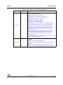
Table 9. Solder bridges
Bridge
State
(1)
Description
OFF
X3, C33, C34, R35 and R37 provide a clock as shown in Chapter 7: Electrical
schematics PF0/PD0/PH0, PF1/PD1/PH1 are disconnected from CN7.
ON
PF0/PD0/PH0, PF1/PD1/PH1 are connected to CN12. (R35, R37 and SB50
must not be fitted).
SB3,5,7,9 (DEFAULT)
ON
Reserved, do not modify.
SB4,6,8,10 (RESERVED)
OFF
Reserved, do not modify.
SB48,49
(X2 crystal)(3)
OFF
X2, C31, C32, R34 and R36 deliver a 32 kHz clock. PC14, PC15 are not
connected to CN7.
ON
PC14, PC15 are only connected to CN7. Remove only R34, R36
SB17
(B1-USER)
ON
B1 push button is connected to PC13.
OFF
B1 push button is not connected to PC13.
ON
The NRST signal of the CN4 connector is connected to the NRST pin of the
STM32 MCU.
OFF
The NRST signal of the CN4 connector is not connected to the NRST pin of
the STM MCU.
ON
The SWO signal of the CN4 connector is connected to PB3.
OFF
The SWO signal is not connected.
OFF
No incidence on STM32F103CBT6 (ST-LINK MCU) NRST signal.
ON
STM32F103CBT6 (ST-LINK MCU) NRST signal is connected to GND.
OFF
USB power management is functional.
ON
USB power management is disabled.
SB54, SB55 (X3 crystal)(2)
SB12 (NRST)
SB15 (SWO)
SB11 (STM_RST)
SB1 (USB-5V)
DocID025833 Rev 8
19/62
61
Hardware layout and configuration
UM1724
Table 9. Solder bridges (continued)
Bridge
SB2 (3.3 V)
SB21 (LD2-LED)
State
ON
Output of voltage regulator LD39050PU33R is connected to 3.3V.
OFF
Output of voltage regulator LD39050PU33R is not connected.
ON
Green user LED LD2 is connected to D13 of Arduino signal.
OFF
Green user LED LD2 is not connected.
ON
PC1 and PC0 (ADC in) are connected to A4 and A5 (pin 5 and pin 6) on
Arduino connector CN8 and ST Morpho connector CN7. Thus SB46 and
SB52 should be OFF.
OFF
PC1 and PC0 (ADC in) are disconnected to A4 and A5 (pin 5 and pin 6) on
Arduino connector CN8 and ST Morpho connector CN7.
OFF
PB9 and PB8 (I2C) are disconnected to A4 and A5 (pin 5 and pin 6) on
Arduino connector CN8 and ST Morpho connector CN7.
ON
PB9 and PB8 (I2C) are connected to A4 and A5 (pin 5 and pin 6) on Arduino
connector CN8 and ST Morpho connector CN7 as I2C signals. Thus SB56
and SB51 should be OFF.
ON
VBAT or VLCD on STM32 MCU is connected to VDD.
OFF
VBAT or VLCD on STM32 MCU is not connected to VDD.
ON
VDDA/VREF+ on STM32 MCU is connected to VDD.
OFF
VDDA/VREF+ on STM32 MCU is not connected to VDD and can be provided
from pin 7 of CN10
ON
PA2 and PA3 on STM32 MCU are connected to D1 and D0 (pin 2 and pin 1)
on Arduino connector CN9 and ST Morpho connector CN10 as USART
signals. Thus SB13 and SB14 should be OFF.
OFF
PA2 and PA3 on STM32 MCU are disconnected to D1 and D0 (pin 2 and pin
1) on Arduino connector CN9 and ST Morpho connector CN10.
OFF
PA2 and PA3 on STM32F103CBT6 (ST-LINK MCU) are disconnected to PA3
and PA2 on STM32 MCU.
ON
PA2 and PA3 on STM32F103CBT6 (ST-LINK MCU) are connected to PA3
and PA2 on STM32 MCU to have USART communication between them.
Thus SB61,SB62 and SB63 should be OFF.
OFF
MCO on STM32F103CBT6 (ST-LINK MCU) are disconnected to
PF0/PD0/PH0 on STM32 MCU.
ON
MCO on STM32F103CBT6 (ST-LINK MCU) are connected to PF0/PD0/PH0
on STM32 MCU.
SB56,SB51 (A4 and A5)
SB46,SB52
(I2C on A4 and A5)
SB45 (VBAT/VLCD)
SB57 (VDDA/VREF+)
Description
(1)
SB62, SB63 (USART)
SB13, SB14
(ST-LINK-USART)
SB16,SB50(MCO)(2)
1. The default SBx state is shown in bold.
2. Default configuration depends on board version. Please refer to chapter 5.7.1 for details
3. Default configuration depends on board version. Please refer to chapter 5.7.2 for details.
All the other solder bridges present on the STM32 Nucleo board are used to configure
several IOs and power supply pins for compatibility of features and pinout with STM32 MCU
supported.
20/62
DocID025833 Rev 8
UM1724
Hardware layout and configuration
All STM32 Nucleo boards are delivered with the solder-bridges configured according to the
target MCU supported.
5.9
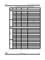
Extension connectors
The following figures show the signals connected by default to Arduino Uno Revision 3
connectors (CN5, CN6, CN8, CN9) and to STMicroelectronics Morpho connector (CN7 and
CN10), for each STM32 Nucleo board.
Figure 8. NUCLEO-F030R8
18&/(2)5
&1 &1
3&
3&
9''
%227
3)
3)
3$
3$
3$
*1'
3%
3&
3&
3&
3)
3)
9%$7
3&
3&
3&
3'
(9
*1'
1&
,25()
5(6(7
9
9
*1'
*1'
9,1
1&
3$
3$
3$
3%
3&
3&
1&
,25()
5(6(7
9
9
*1'
*1'
9,1
$
$
$
$
$
$
3&
' 3%
' 3%
$9'' $9''
*1' *1'
' 3$
' 3$
3$
'
' 3%
' 3&
3$
'
3$
'
' 3%
3%
'
3%
'
3%
'
' 3$
3$
'
3$
'
&1
&1 &1
3&
3&
3&
89
1&
3$
3$
3%
3%
*1'
3%
3%
3%
3%
3%
$*1'
3&
3)
3)
&1
$UGXLQR
0RUSKR
06Y9
Figure 9. NUCLEO-F070RB
18&/(2)5%
&1 &1
3&
3&
9''
%227
1&
1&
3$
3$
3$
*1'
3%
3&
3&
3&
3)
3)
9''
3&
3&
3&
3'
(9
*1'
1&
,25()
5(6(7
9
9
*1'
*1'
9,1
1&
3$
3$
3$
3%
3&
3&
1&
,25()
5(6(7
9
9
*1'
*1'
9,1
$
$
$
$
$
$
3&
' 3%
' 3%
$9'' $9''
*1' *1'
' 3$
' 3$
3$
'
' 3%
' 3&
3$
'
3$
'
' 3%
3%
'
3%
'
3%
'
' 3$
3$
'
3$
'
&1
&1 &1
3&
3&
3&
89
1&
3$
3$
3%
3%
*1'
3%
3%
3%
3%
3%
$*1'
3&
1&
1&
&1
$UGXLQR
DocID025833 Rev 8
0RUSKR
06Y9
21/62
61
Hardware layout and configuration
UM1724
Figure 10. NUCLEO-F072RB
18&/(2)5%
&1 &1
3&
3&
9''
%227
1&
1&
3$
3$
3$
*1'
3%
3&
3&
3&
3)
3)
9%$7
3&
3&
3&
3'
(9
*1'
1&
,25()
5(6(7
9
9
*1'
*1'
9,1
1&
3$
3$
3$
3%
3&
3&
1&
,25()
5(6(7
9
9
*1'
*1'
9,1
$
$
$
$
$
$
3&
' 3%
' 3%
$9'' $9''
*1' *1'
' 3$
' 3$
3$
'
' 3%
' 3&
3$
'
3$
'
' 3%
3%
'
3%
'
3%
'
' 3$
3$
'
3$
'
&1
&1 &1
3&
3&
3&
89
1&
3$
3$
3%
3%
*1'
3%
3%
3%
3%
3%
$*1'
3&
1&
1&
&1
$UGXLQR
0RUSKR
06Y9
Figure 11. NUCLEO-F091RC
18&/(2)5&
&1 &1
3&
3&
9''
3)%227
1&
1&
3$
3$
3$
*1'
3%
3&
3&
3&
3)
3)
9%$7
3&
3&
3&
3'
(9
*1'
1&
,25()
5(6(7
9
9
*1'
*1'
9,1
1&
3$
3$
3$
3%
3&
3&
1&
,25()
5(6(7
9
9
*1'
*1'
9,1
$
$
$
$
$
$
3&
' 3%
' 3%
$9'' $9''
*1' *1'
' 3$
' 3$
3$
'
' 3%
' 3&
3$
'
3$
'
' 3%
3%
'
3%
'
3%
'
' 3$
3$
'
3$
'
&1
3&
3&
3&
89
1&
3$
3$
3%
3%
*1'
3%
3%
3%
3%
3%
$*1'
3&
1&
1&
&1
$UGXLQR
22/62
&1 &1
DocID025833 Rev 8
0RUSKR
06Y9
UM1724
Hardware layout and configuration
Figure 12. NUCLEO-F103RB
18&/(2)5%
&1 &1
3&
3&
9''
%227
1&
1&
3$
3$
3$
*1'
3%
3&
3&
3&
3'
3'
9%$7
3&
3&
3&
3'
(9
*1'
1&
,25()
5(6(7
9
9
*1'
*1'
9,1
1&
3$
3$
3$
3%
3&
3&
1&
,25()
5(6(7
9
9
*1'
*1'
9,1
$
$
$
$
$
$
3&
' 3%
' 3%
$9'' $9''
*1' *1'
' 3$
' 3$
'
3$
' 3%
' 3&
'
3$
'
3$
' 3%
'
3%
'
3%
'
3%
' 3$
'
3$
'
3$
&1
&1 &1
3&
3&
3&
89
1&
3$
3$
3%
3%
*1'
3%
3%
3%
3%
3%
$*1'
3&
1&
1&
&1
$UGXLQR
0RUSKR
06Y9
Figure 13. NUCLEO-F302R8
18&/(2)5
&1 &1
3&
3&
9''
%227
1&
1&
3$
3$
3$
*1'
3%
3&
3&
3&
3)
3)
9%$7
3&
3&
3&
3'
(9
*1'
1&
,25()
5(6(7
9
9
*1'
*1'
9,1
1&
3$
3$
3$
3%
3&
3&
1&
,25()
5(6(7
9
9
*1'
*1'
9,1
$
$
$
$
$
$
'
'
$9''
*1'
'
'
'
'
'
'
3&
3%
3%
$9''
*1'
3%
3%
3%
3%
3&
3$
3$
'
' 3%
3%
'
3%
'
3%
'
' 3$
3$
'
3$
'
&1
&1 &1
3&
3&
3&
89
1&
3$
3$
3%
3%
*1'
3%
3%
3$
3$
3$
$*1'
3&
1&
1&
&1
$UGXLQR
DocID025833 Rev 8
0RUSKR
06Y9
23/62
61
Hardware layout and configuration
UM1724
Figure 14. NUCLEO-F303RE
18&/(2)5(
&1 &1
3&
3&
9''
%227
1&
1&
3$
3$
3$
*1'
3%
3&
3&
3&
3)
3)
9%$7
3&
3&
3&
3'
(9
*1'
1&
,25()
5(6(7
9
9
*1'
*1'
9,1
1&
3$
3$
3$
3%
3&
3&
1&
,25()
5(6(7
9
9
*1'
*1'
9,1
$
$
$
$
$
$
3&
' 3%
' 3%
$9'' $9''
*1' *1'
' 3$
' 3$
3$
'
' 3%
' 3&
3$
'
3$
'
' 3%
3%
'
3%
'
3%
'
' 3$
3$
'
3$
'
&1
&1 &1
3&
3&
3&
89
1&
3$
3$
3%
3%
*1'
3%
3%
3%
3%
3%
$*1'
3&
1&
1&
&1
$UGXLQR
0RUSKR
06Y9
Figure 15. NUCLEO-F334R8
18&/(2)5
&1 &1
3&
3&
9''
%227
1&
1&
3$
3$
3$
*1'
3%
3&
3&
3&
3)
3)
9%$7
3&
3&
3&
3'
(9
*1'
1&
,25()
5(6(7
9
9
*1'
*1'
9,1
1&
3$
3$
3$
3%
3&
3&
1&
,25()
5(6(7
9
9
*1'
*1'
9,1
$
$
$
$
$
$
3&
' 3%
' 3%
$9'' $9''
*1' *1'
' 3$
' 3$
3$
'
' 3%
' 3&
3$
'
3$
'
' 3%
3%
'
3%
'
3%
'
' 3$
3$
'
3$
'
&1
3&
3&
3&
89
1&
3$
3$
3%
3%
*1'
3%
3%
3%
3%
3%
$*1'
3&
1&
1&
&1
$UGXLQR
24/62
&1 &1
DocID025833 Rev 8
0RUSKR
06Y9
UM1724
Hardware layout and configuration
Figure 16. NUCLEO-F401RE
18&/(2)5(
&1 &1
3&
3&
9''
%227
1&
1&
3$
3$
3$
*1'
3%
3&
3&
3&
3+
3+
9%$7
3&
3&
3&
3'
(9
*1'
1&
,25()
5(6(7
9
9
*1'
*1'
9,1
1&
3$
3$
3$
3%
3&
3&
1&
,25()
5(6(7
9
9
*1'
*1'
9,1
$
$
$
$
$
$
3&
' 3%
' 3%
$9'' $9''
*1' *1'
' 3$
' 3$
3$
'
' 3%
' 3&
3$
'
3$
'
' 3%
3%
'
3%
'
3%
'
' 3$
3$
'
3$
'
&1
&1 &1
3&
3&
3&
89
1&
3$
3$
3%
1&
*1'
3%
3%
3%
3%
3%
$*1'
3&
1&
1&
&1
$UGXLQR
0RUSKR
06Y9
Figure 17. NUCLEO-F411RE
18&/(2)5(
&1 &1
3&
3&
9''
%227
1&
1&
3$
3$
3$
*1'
3%
3&
3&
3&
3+
3+
9%$7
3&
3&
3&
3'
(9
*1'
1&
,25()
5(6(7
9
9
*1'
*1'
9,1
1&
3$
3$
3$
3%
3&
3&
1&
,25()
5(6(7
9
9
*1'
*1'
9,1
$
$
$
$
$
$
3&
' 3%
' 3%
$9'' $9''
*1' *1'
' 3$
' 3$
3$
'
' 3%
' 3&
3$
'
3$
'
' 3%
3%
'
3%
'
3%
'
' 3$
3$
'
3$
'
&1
&1 &1
3&
3&
3&
89
1&
3$
3$
3%
1&
*1'
3%
3%
3%
3%
3%
$*1'
3&
1&
1&
&1
$UGXLQR
0RUSKR
06Y9
DocID025833 Rev 8
25/62
61
Hardware layout and configuration
UM1724
Figure 18. NUCLEO-L053R8
18&/(2/5
&1 &1
3&
3&
9''
%227
1&
1&
3$
3$
3$
*1'
3%
3&
3&
3&
3+
3+
9/&'
3&
3&
3&
3'
(9
*1'
1&
,25()
5(6(7
9
9
*1'
*1'
9,1
1&
3$
3$
3$
3%
3&
3&
1&
,25()
5(6(7
9
9
*1'
*1'
9,1
$
$
$
$
$
$
3&
' 3%
' 3%
$9'' $9''
*1' *1'
' 3$
' 3$
3$
'
' 3%
' 3&
3$
'
3$
'
' 3%
3%
'
3%
'
3%
'
' 3$
3$
'
3$
'
&1
&1 &1
3&
3&
3&
89
1&
3$
3$
3%
3%
*1'
3%
3%
3%
3%
3%
$*1'
3&
1&
1&
&1
$UGXLQR
0RUSKR
06Y9
Figure 19. NUCLEO-L073RZ
18&/(2/5=
&1 &1
3&
3&
9''
%227
1&
1&
3$
3$
3$
*1'
3%
3&
3&
3&
3+
3+
9/&'
3&
3&
3&
3'
(9
*1'
1&
,25()
5(6(7
9
9
*1'
*1'
9,1
1&
3$
3$
3$
3%
3&
3&
1&
,25()
5(6(7
9
9
*1'
*1'
9,1
$
$
$
$
$
$
3&
' 3%
' 3%
$9'' $9''
*1' *1'
' 3$
' 3$
3$
'
' 3%
' 3&
3$
'
3$
'
' 3%
3%
'
3%
'
3%
'
' 3$
3$
'
3$
'
&1
&1 &1
3&
3&
3&
89
1&
3$
3$
3%
3%
*1'
3%
3%
3%
3%
3%
$*1'
3&
1&
1&
&1
$UGXLQR
0RUSKR
06Y9
26/62
DocID025833 Rev 8
UM1724
Hardware layout and configuration
Figure 20. NUCLEO-L152RE
18&/(2/5(
&1 &1
3&
3&
9''
%227
1&
1&
3$
3$
3$
*1'
3%
3&
3&
3&
3+
3+
9/&'
3&
3&
3&
3'
(9
*1'
1&
,25()
5(6(7
9
9
*1'
*1'
9,1
1&
3$
3$
3$
3%
3&
3&
1&
,25()
5(6(7
9
9
*1'
*1'
9,1
$
$
$
$
$
$
3&
' 3%
' 3%
$9'' $9''
*1' *1'
' 3$
' 3$
3$
'
' 3%
' 3&
3$
'
3$
'
' 3%
3%
'
3%
'
3%
'
' 3$
3$
'
3$
'
&1
&1 &1
3&
3&
3&
89
1&
3$
3$
3%
3%
*1'
3%
3%
3%
3%
3%
$*1'
3&
1&
1&
&1
$UGXLQR
0RUSKR
06Y9
Figure 21. NUCLEO-L476RG
18&/(2/5*
&1 &1
3&
3&
9''
%227
1&
1&
3$
3$
3$
*1'
3%
3&
3&
3&
3+
3+
9%$7
3&
3&
3&
3'
(9
*1'
1&
,25()
5(6(7
9
9
*1'
*1'
9,1
1&
3$
3$
3$
3%
3&
3&
1&
,25()
5(6(7
9
9
*1'
*1'
9,1
$
$
$
$
$
$
3&
' 3%
' 3%
$9'' $9''
*1' *1'
' 3$
' 3$
3$
'
' 3%
' 3&
3$
'
3$
'
' 3%
3%
'
3%
'
3%
'
' 3$
3$
'
3$
'
&1
&1 &1
3&
3&
3&
89
1&
3$
3$
3%
3%
*1'
3%
3%
3%
3%
3%
$*1'
3&
1&
1&
&1
$UGXLQR
0RUSKR
06Y9
DocID025833 Rev 8
27/62
61
Hardware layout and configuration
UM1724
Figure 22. NUCLEO-F446RE
18&/(2)5(
Eϳ
WϭϬ
WϭϮ
s
KKdϬ
E
E
Wϭϯ
Wϭϰ
Wϭϱ
'E
Wϳ
Wϭϯ
Wϭϰ
Wϭϱ
W,Ϭ
W,ϭ
sd
WϮ
Wϯ
ϭ
ϯ
ϱ
ϳ
ϵ
ϭϭ
ϭϯ
ϭϱ
ϭϳ
ϭϵ
Ϯϭ
Ϯϯ
Ϯϱ
Ϯϳ
Ϯϵ
ϯϭ
ϯϯ
ϯϱ
ϯϳ
Ϯ
ϰ
ϲ
ϴ
ϭϬ
ϭϮ
ϭϰ
ϭϲ
ϭϴ
ϮϬ
ϮϮ
Ϯϰ
Ϯϲ
Ϯϴ
ϯϬ
ϯϮ
ϯϰ
ϯϲ
ϯϴ
Eϲ
Wϭϭ
WϮ
ϱs
'E
E
/KZ&
Z^d
нϯsϯ
нϱs
'E
'E
s/E
E
WϬ
Wϭ
Wϰ
WϬ
Wϭ
WϬ
ϭ
Ϯ
ϯ
ϰ
ϱ
ϲ
ϳ
ϴ
ϭ
Ϯ
ϯ
ϰ
ϱ
ϲ
E
/KZ&
Z^d
нϯsϯ
нϱs
'E
'E
s/E
Ϭ
ϭ
Ϯ
ϯ
ϰ
ϱ
Wϵ
Wϴ
ϭϱ
Wϵ
ϭϰ
s s
'E 'E
Wϱ
ϭϯ
Wϲ
ϭϮ
Wϳ
ϭϭ
Wϲ
ϭϬ
Wϳ
ϵ
Wϵ
ϴ
Wϴ
WϭϬ
Wϰ
Wϱ
Wϯ
WϭϬ
WϮ
Wϯ
ϳ
ϲ
ϱ
ϰ
ϯ
Ϯ
ϭ
Ϭ
Eϴ
Eϱ EϭϬ
ϭϬ
ϵ
ϴ
ϳ
ϲ
ϱ
ϰ
ϯ
Ϯ
ϭ
ϴ
ϳ
ϲ
ϱ
ϰ
ϯ
Ϯ
ϭ
ϭ
ϯ
ϱ
ϳ
ϵ
ϭϭ
ϭϯ
ϭϱ
ϭϳ
ϭϵ
Ϯϭ
Ϯϯ
Ϯϱ
Ϯϳ
Ϯϵ
ϯϭ
ϯϯ
ϯϱ
ϯϳ
Ϯ
ϰ
ϲ
ϴ
ϭϬ
ϭϮ
ϭϰ
ϭϲ
ϭϴ
ϮϬ
ϮϮ
Ϯϰ
Ϯϲ
Ϯϴ
ϯϬ
ϯϮ
ϯϰ
ϯϲ
ϯϴ
Wϴ
Wϲ
Wϱ
hϱs
E
WϭϮ
Wϭϭ
WϭϮ
E
'E
WϮ
Wϭ
Wϭϱ
Wϭϰ
Wϭϯ
'E
Wϰ
E
E
Eϵ
ƌĚƵŝŶŽ
DŽƌƉŚŽ
06Y9
Figure 23. NUCLEO-F410RB
18&/(2)5%
&1 &1
3&
3&
9''
%227
1&
1&
3$
3$
3$
*1'
3%
3&
3&
3&
3+
3+
9%$7
3&
3&
3&
3%
(9
*1'
1&
,25()
5(6(7
9
9
*1'
*1'
9,1
1&
3$
3$
3$
3%
3&
3&
1&
,25()
5(6(7
9
9
*1'
*1'
9,1
$
$
$
$
$
$
3&
' 3%
' 3%
$9'' $9''
*1' *1'
' 3$
' 3$
3$
'
' 3%
' 3&
3$
'
3$
'
' 3%
3%
'
3%
'
3%
'
' 3$
3$
'
3$
'
&1
&1 &1
3&
3&
3&
89
1&
3$
3$
3%
1&
*1'
3%
3%
3%
3%
3%
$*1'
3&
1&
1&
&1
$UGXLQR
0RUSKR
06Y9
28/62
DocID025833 Rev 8
UM1724
5.10
Hardware layout and configuration
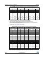
Arduino connectors
CN5, CN6, CN8 and CN9 are female connectors compatible with Arduino standard. Most
shields designed for Arduino can fit to the STM32 Nucleo boards.
The Arduino connectors on STM32 Nucleo board support the Arduino Uno Revision 3.
For compatibility with Arduino Uno Revision 1, apply the following modifications:
Caution:
SB46 and SB52 should be ON,
SB51 and SB56 should be OFF to connect I2C on A4 (pin 5) and A5 (pin 6 of CN8).
The IOs of STM32 microcontroller are 3.3 V compatible instead of 5 V for Arduino Uno.
Table 10 to Table 21 show the pin assignment of each main STM32 microcontroller on
Arduino connectors.
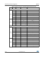
Table 10. Arduino connectors on
NUCLEO-F030R8, NUCLEO-F070RB, NUCLEO-F072RB, NUCLEO-F091RC
CN No.
Pin No.
Pin name
MCU pin
Function
1
NC
-
-
2
IOREF
-
3.3V Ref
3
RESET
NRST
RESET
4
+3V3
-
3.3V input/output
5
+5V
-
5V output
6
GND
-
Ground
7
GND
-
Ground
8
VIN
-
Power input
1
A0
PA0
ADC_IN0
2
A1
PA1
ADC_IN1
3
A2
PA4
ADC_IN4
4
A3
PB0
ADC_IN8
Left connectors
CN6
power
CN8
analog
5
6
A4
A5
PC1 or
PB9(1)
ADC_IN11 (PC1) or I2C1_SDA (PB9)
(1)
ADC_IN10 (PC0) or I2C1_SCL (PB8)
PC0 or PB8
DocID025833 Rev 8
29/62
61
Hardware layout and configuration
UM1724
Table 10. Arduino connectors on
NUCLEO-F030R8, NUCLEO-F070RB, NUCLEO-F072RB, NUCLEO-F091RC (continued)
CN No.
Pin No.
Pin name
MCU pin
Function
10
D15
PB8
I2C1_SCL
9
D14
PB9
I2C1_SDA
8
AREF
-
AVDD
7
GND
-
Ground
6
D13
PA5
SPI1_SCK
5
D12
PA6
SPI1_MISO
4
D11
PA7
TIM17_CH1 or SPI1_MOSI
3
D10
PB6
TIM16_CH1N or SPI1_CS
2
D9
PC7
TIM3_CH2
1
D8
PA9
-
8
D7
PA8
-
7
D6
PB10
TIM2_CH3(2)
6
D5
PB4
TIM3_CH1
5
D4
PB5
-
4
D3
PB3
TIM2_CH2(3)
3
D2
PA10
-
2
D1
PA2
USART2_TX
1
D0
PA3
USART2_RX
Right connectors
CN5
digital
CN9
digital
1. Please refer to Table 9: Solder bridges for details.
2. Warning: PWM is not supported by D6 on STM32F030 and STM32F070 since the timer is not available on
PB10.
3. Warning: PWM is not supported by D3 on STM32F030 and STM32F070 since timer is not available on
PB3.
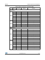
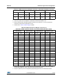
Table 11. Arduino connectors on NUCLEO-F103RB
CN No.
Pin No.
Pin name
MCU pin
Function
1
NC
-
-
2
IOREF
-
3.3V Ref
3
RESET
NRST
RESET
4
+3V3
-
3.3V input/output
5
+5V
-
5V output
6
GND
-
Ground
7
GND
-
Ground
8
VIN
-
Power input
Left connectors
CN6
power
30/62
DocID025833 Rev 8
UM1724
Hardware layout and configuration
Table 11. Arduino connectors on NUCLEO-F103RB (continued)
CN No.
CN8
analog
Pin No.
Pin name
MCU pin
Function
1
A0
PA0
ADC_0
2
A1
PA1
ADC_1
3
A2
PA4
ADC_4
4
A3
PB0
ADC_8
5
6
A4
A5
PC1 or
PB9(1)
ADC_11 (PC1) or I2C1_SDA (PB9)
(1)
ADC_10 (PC0) or I2C1_SCL (PB8)
PC0 or PB8
Right connectors
CN5
digital
CN9
digital
10
D15
PB8
I2C1_SCL
9
D14
PB9
I2C1_SDA
8
AREF
-
AVDD
7
GND
-
Ground
6
D13
PA5
SPI1_SCK
5
D12
PA6
SPI1_MISO
4
D11
PA7
TIM3_CH2 or SPI1_MOSI
3
D10
PB6
TIM4_CH1 or SPI1_CS
2
D9
PC7
TIM3_CH2
1
D8
PA9
-
8
D7
PA8
-
7
D6
PB10
TIM2_CH3
6
D5
PB4
TIM3_CH1
5
D4
PB5
-
4
D3
PB3
TIM2_CH2
3
D2
PA10
-
2
D1
PA2
USART2_TX
1
D0
PA3
USART2_RX
1. Please refer to Table 9: Solder bridges for detail.
DocID025833 Rev 8
31/62
61
Hardware layout and configuration
UM1724
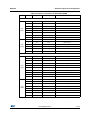
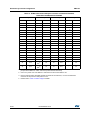
Table 12. Arduino connectors on NUCLEO-F302R8
CN No.
Pin No.
Pin name
MCU pin
Function
1
NC
-
-
2
IOREF
-
3.3V Ref
3
RESET
NRST
RESET
4
+3V3
-
3.3V input/output
5
+5V
-
5V output
6
GND
-
Ground
7
GND
-
Ground
8
VIN
-
Power input
1
A0
PA0
ADC_IN1
2
A1
PA1
ADC_IN2
3
A2
PA4
ADC_IN5
4
A3
PB0
Left connectors
CN6
Power
CN8
Analog
5
6
A4
A5
ADC_IN11
(1)
ADC_IN7 (PC1) or I2C1_SDA (PB9)
(1)
ADC_IN6 (PC0) or I2C1_SCL (PB8)
PC1 or PB9
PC0 or PB8
Right connectors
CN5
digital
CN9
digital
10
D15
PB8
I2C1_SCL
9
D14
PB9
I2C1_SDA
8
AREF
-
AVDD
7
GND
-
Ground
6
D13
PB13
SPI2_SCK
5
D12
PB14
SPI2_MISO
4
D11
PB15
TIM15_CH2 or SPI2_MOSI
3
D10
PB6
TIM16_CH1N or SPI2_CS
2
D9
PC7
-
1
D8
PA9
-
8
D7
PA8
-
7
D6
PB10
TIM2_CH3
6
D5
PB4
TIM16_CH1
5
D4
PB5
-
4
D3
PB3
TIM2_CH2
3
D2
PA10
-
2
D1
PA2
USART2_TX
1
D0
PA3
USART2_RX
1. Please refer to Table 9: Solder bridges for details.
32/62
DocID025833 Rev 8
UM1724
Hardware layout and configuration
Warning:
PWM is not supported by D9 on STM32F302 since the timer is
not available on PC7.
DocID025833 Rev 8
33/62
61
Hardware layout and configuration
UM1724
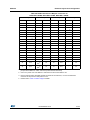
Table 13. Arduino connectors on NUCLEO-F303RE
CN No.
Pin No.
Pin name
MCU pin
Function
1
NC
-
-
2
IOREF
-
3.3V Ref
3
RESET
NRST
RESET
4
+3V3
-
3.3V input/output
5
+5V
-
5V output
6
GND
-
Ground
7
GND
-
Ground
8
VIN
-
Power input
1
A0
PA0
ADC1_IN1
2
A1
PA1
ADC1_IN2
3
A2
PA4
ADC2_IN1
4
A3
PB0
ADC3_IN12
5
A4
PC1 or PB9(1)
ADC12_IN7 (PC1) or I2C1_SDA (PB9)
6
A5
PC0 or PB8(1)
ADC12_IN6 (PC0) or I2C1_SCL (PB8)
10
D15
PB8
I2C1_SCL
9
D14
PB9
I2C1_SDA
8
AREF
-
AVDD
7
GND
-
Ground
6
D13
PA5
SPI1_SCK
5
D12
PA6
SPI1_MISO
4
D11
PA7
TIM17_CH1 or SPI1_MOSI
3
D10
PB6
TIM4_CH1 or SPI1_CS
2
D9
PC7
TIM3_CH2
1
D8
PA9
-
8
D7
PA8
-
7
D6
PB10
TIM2_CH3
6
D5
PB4
TIM3_CH1
5
D4
PB5
-
4
D3
PB3
TIM2_CH2
3
D2
PA10
-
2
D1
PA2
USART2_TX
Left connectors
CN6
Power
CN8
Analog
Right connectors
CN5
Digital
CN9
Digital
1. Please refer to Table 9: Solder bridges or details.
34/62
DocID025833 Rev 8
UM1724
Hardware layout and configuration
Table 14. Arduino connectors on NUCLEO-F334R8
CN No.
Pin No.
Pin name
MCU pin
Function
1
NC
-
-
2
IOREF
-
3.3V Ref
3
RESET
NRST
RESET
4
+3V3
-
3.3V input/output
5
+5V
-
5V output
6
GND
-
Ground
7
GND
-
Ground
8
VIN
-
Power input
1
A0
PA0
ADC1_IN1
2
A1
PA1
ADC1_IN2
3
A2
PA4
ADC2_IN1
4
A3
PB0
Left connectors
CN6
power
CN8
analog
5
6
A4
A5
ADC1_IN11
(1)
ADC_IN7 (PC1) or I2C1_SDA (PB9)
PB8(1)
ADC_IN6 (PC0) or I2C1_SCL (PB8)
PC1 or PB9
PC0 or
Right connectors
CN5
digital
CN9
digital
10
D15
PB8
I2C1_SCL
9
D14
PB9
I2C1_SDA
8
AREF
-
AVDD
7
GND
-
Ground
6
D13
PA5
SPI1_SCK
5
D12
PA6
SPI1_MISO
4
D11
PA7
TIM17_CH1 or SPI1_MOSI
3
D10
PB6
TIM16_CH1N or SPI1_CS
2
D9
PC7
TIM3_CH2
1
D8
PA9
-
8
D7
PA8
-
7
D6
PB10
TIM2_CH3
6
D5
PB4
TIM3_CH1
5
D4
PB5
-
4
D3
PB3
TIM2_CH2
3
D2
PA10
-
2
D1
PA2
USART2_TX
1
D0
PA3
USART2_RX
1. Please refer to Table 9: Solder bridges for details.
DocID025833 Rev 8
35/62
61
Hardware layout and configuration
UM1724
Table 15. Arduino connectors on NUCLEO-F401RE, NUCLEO-F411RE
CN No.
Pin No.
Pin name
MCU pin
Function
1
NC
-
-
2
IOREF
-
3.3V Ref
3
RESET
NRST
RESET
4
+3V3
-
3.3V input/output
5
+5V
-
5V output
6
GND
-
Ground
7
GND
-
Ground
8
VIN
-
Power input
1
A0
PA0
ADC1_0
2
A1
PA1
ADC1_1
3
A2
PA4
ADC1_4
4
A3
PB0
Left connectors
CN6
power
CN8
analog
5
6
A4
A5
ADC1_8
(1)
ADC1_11 (PC1) or I2C1_SDA (PB9)
PB8(1)
ADC1_10 (PC0) or I2C1_SCL (PB8)
PC1 or PB9
PC0 or
Right connectors
CN5
digital
CN9
digital
10
D15
PB8
I2C1_SCL
9
D14
PB9
I2C1_SDA
8
AREF
-
AVDD
7
GND
-
Ground
6
D13
PA5
SPI1_SCK
5
D12
PA6
SPI1_MISO
4
D11
PA7
TIM1_CH1N or SPI1_MOSI
3
D10
PB6
TIM4_CH1 or SPI1_CS
2
D9
PC7
TIM3_CH2
1
D8
PA9
-
8
D7
PA8
-
7
D6
PB10
TIM2_CH3
6
D5
PB4
TIM3_CH1
5
D4
PB5
-
4
D3
PB3
TIM2_CH2
3
D2
PA10
-
2
D1
PA2
USART2_TX
1
D0
PA3
USART2_RX
1. Please refer to Table 9: Solder bridges for details.
36/62
DocID025833 Rev 8
UM1724
Hardware layout and configuration
Table 16. Arduino connectors on NUCLEO-L053R8
Connect
or No.
Pin No.
Pin name
MCU pin
Function
1
NC
-
-
2
IOREF
-
3.3V Ref
3
RESET
NRST
RESET
4
+3V3
-
3.3V input/output
5
+5V
-
5V output
6
GND
-
Ground
7
GND
-
Ground
8
VIN
-
Power input
1
A0
PA0
ADC_IN0
2
A1
PA1
ADC_IN1
3
A2
PA4
ADC_IN4
4
A3
PB0
ADC_IN8
Left connectors
CN6
power
CN8
analog
5
6
A4
A5
PC1 or
PB9(1)
ADC_IN11 (PC1) or I2C1_SDA (PB9)
(1)
ADC_IN10 (PC0) or I2C1_SCL (PB8)
PC0 or PB8
Right connectors
CN5
digital
CN9
digital
10
D15
PB8
I2C1_SCL
9
D14
PB9
I2C1_SDA
8
AREF
-
AVDD
7
GND
-
Ground
6
D13
PA5
SPI1_SCK
5
D12
PA6
SPI1_MISO
4
D11
PA7
TIM12_CH2 or SPI1_MOSI
3
D10
PB6
SPI1_CS
2
D9
PC7
TIM12_CH2
1
D8
PA9
-
8
D7
PA8
-
7
D6
PB10
TIM2_CH3
6
D5
PB4
TIM12_CH1
5
D4
PB5
-
4
D3
PB3
TIM2_CH2
3
D2
PA10
-
2
D1
PA2
USART2_TX
1
D0
PA3
USART2_RX
1. Please refer to Table 9: Solder bridges for details.
DocID025833 Rev 8
37/62
61
Hardware layout and configuration
Warning:
38/62
UM1724
PWM is not supported by D10 on STM32L053 since the timer
is not available on PB6.
DocID025833 Rev 8
UM1724
Hardware layout and configuration
Table 17. Arduino connectors on NUCLEO-L073RZ
CN No.
Pin No.
Pin name
MCU pin
Function
1
NC
-
-
2
IOREF
-
3.3V Ref
3
RESET
NRST
RESET
4
+3V3
-
3.3V input/output
5
+5V
-
5V output
6
GND
-
Ground
7
GND
-
Ground
8
VIN
-
Power input
1
A0
PA0
ADC_IN0
2
A1
PA1
ADC_IN1
3
A2
PA4
ADC_IN4
4
A3
PB0
Left connectors
CN6
power
CN8
analog
5
6
A4
A5
ADC_IN8
(1)
ADC_IN11 (PC1) or I2C1_SDA (PB9)
PB8(1)
ADC_IN10 (PC0) or I2C1_SCL (PB8)
PC1 or PB9
PC0 or
Right connectors
CN5
digital
CN9
digital
10
D15
PB8
I2C1_SCL
9
D14
PB9
I2C1_SDA
8
AREF
-
AVDD
7
GND
-
Ground
6
D13
PA5
SPI1_SCK
5
D12
PA6
SPI1_MISO
4
D11
PA7
TIM22_CH2 or SPI1_MOSI
3
D10
PB6
SPI1_CS
2
D9
PC7
TIM3_CH2
1
D8
PA9
-
8
D7
PA8
-
7
D6
PB10
TIM2_CH3
6
D5
PB4
TIM3_CH1
5
D4
PB5
-
4
D3
PB3
TIM2_CH2
3
D2
PA10
-
2
D1
PA2
USART2_TX
1
D0
PA3
USART2_RX
1. Please refer to Table 9: Solder bridges for details.
DocID025833 Rev 8
39/62
61
Hardware layout and configuration
Warning:
40/62
UM1724
PWM is not supported by D10 on STM32L073 since the timer
is not available on PB6.
DocID025833 Rev 8
UM1724
Hardware layout and configuration
Table 18. Arduino connectors on NUCLEO-F446RE
CN No.
Pin No.
Pin name
MCU pin
Function
1
NC
-
-
2
IOREF
-
3.3V Ref
3
RESET
NRST
RESET
4
+3V3
-
3.3V input/output
5
+5V
-
5V output
6
GND
-
Ground
7
GND
-
Ground
8
VIN
-
Power input
1
A0
PA0
ADC123_IN0
2
A1
PA1
ADC123_IN1
3
A2
PA4
ADC12_IN4
4
A3
PB0
Left connectors
CN6
power
CN8
analog
ADC12_IN8
(1)
5
A4
PC1 or PB9
ADC123_IN11 (PC1) or I2C1_SDA (PB9)
6
A5
PC0 or PB8(1)
ADC123_IN10 (PC0) or I2C1_SCL (PB8)
10
D15
PB8
I2C1_SCL
9
D14
PB9
I2C1_SDA
8
AREF
-
AVDD
7
GND
-
Ground
6
D13
PA5
SPI1_SCK
5
D12
PA6
SPI1_MISO
4
D11
PA7
TIM14_CH1 || SPI1_MOSI
3
D10
PB6
TIM4_CH1 || SPI1_CS
2
D9
PC7
TIM8_CH2
1
D8
PA9
-
8
D7
PA8
-
7
D6
PB10
TIM2_CH3
6
D5
PB4
TIM3_CH1
5
D4
PB5
-
4
D3
PB3
TIM2_CH2
3
D2
PA10
-
2
D1
PA2
USART2_TX
1
D0
PA3
USART2_RX
Right connectors
CN5
digital
CN9
digital
1. Please refer to Table 9: Solder bridges for details.
DocID025833 Rev 8
41/62
61
Hardware layout and configuration
UM1724
Table 19. Arduino connectors on NUCLEO-F410RB
CN No.
Pin No.
Pin name
MCU pin
Function
1
NC
-
-
2
IOREF
-
3.3V Ref
3
RESET
NRST
RESET
4
+3V3
-
3.3V input/output
5
+5V
-
5V output
6
GND
-
Ground
7
GND
-
Ground
8
VIN
-
Power input
1
A0
PA0
ADC1_0
2
A1
PA1
ADC1_1
3
A2
PA4
ADC1_4
4
A3
PB0
ADC1_8
Left connectors
CN6
power
CN8
analog
5
6
A4
A5
PC1 or
PB9(1)
ADC1_11 (PC1) or I2C1_SDA (PB9)
(1)
ADC1_10 (PC0) or I2C1_SCL (PB8)
PC0 or PB8
Right connectors
CN5
digital
CN9
digital
42/62
10
PB8
D15
I2C1_SCL
9
PB9
D14
I2C1_SDA
8
-
AREF
AVDD
7
-
GND
Ground
6
PA5
D13
SPI1_SCK
5
PA6
D12
SPI1_MISO
4
PA7
D11
TIM1_CH1N || SPI1_MOSI
3
PB6
D10
SPI1_CS
2
PC7
D9
-
1
PA9
D8
-
8
PA8
D7
-
7
PB10
D6
-
6
PB4
D5
-
5
PB5
D4
-
4
PB3
D3
-
3
PA10
D2
-
2
PA2
D1
USART2_TX
1
PA3
D0
USART2_RX
DocID025833 Rev 8
UM1724
Hardware layout and configuration
1. Please refer to Table 9: Solder bridges for details.
Warning:
PWM is not supported by D3, D5, D6, D9 and D10 on
STM32F410RB since timer is not available on PB6, PC7,
PB10, PB4, PB3.
Table 20. Arduino connectors on NUCLEO-L152RE
CN No.
Pin No.
Pin name
MCU pin
Function
1
NC
-
-
2
IOREF
-
3.3V Ref
3
RESET
NRST
RESET
4
+3V3
-
3.3V input/output
5
+5V
-
5V output
6
GND
-
Ground
7
GND
-
Ground
8
VIN
-
Power input
1
A0
PA0
ADC_IN0
2
A1
PA1
ADC_IN1
3
A2
PA4
ADC_IN4
4
A3
PB0
Left connectors
CN6
power
CN8
analog
5
6
A4
A5
ADC_IN8
(1)
ADC_IN11 (PC1) or I2C1_SDA (PB9)
PB8(1)
ADC_IN10 (PC0) or I2C1_SCL (PB8)
PC1 or PB9
PC0 or
Right connectors
CN5
digital
10
D15
PB8
I2C1_SCL
9
D14
PB9
I2C1_SDA
8
AREF
-
AVDD
7
GND
-
Ground
6
D13
PA5
SPI1_SCK
5
D12
PA6
SPI1_MISO
4
D11
PA7
TIM11_CH1 or SPI1_MOSI
3
D10
PB6
TIM4_CH1 or SPI1_CS
2
D9
PC7
TIM3_CH2
1
D8
PA9
-
DocID025833 Rev 8
43/62
61
Hardware layout and configuration
UM1724
Table 20. Arduino connectors on NUCLEO-L152RE (continued)
CN No.
CN9
digital
Pin No.
Pin name
MCU pin
Function
8
D7
PA8
-
7
D6
PB10
TIM2_CH3
6
D5
PB4
TIM3_CH1
5
D4
PB5
-
4
D3
PB3
TIM2_CH2
3
D2
PA10
-
2
D1
PA2
USART2_TX
1
D0
PA3
USART2_RX
1. Please refer to Table 9: Solder bridges for details.
Table 21. Arduino connectors on NUCLEO-L476RG
CN No.
Pin No.
Pin name
MCU pin
Function
1
NC
-
-
2
IOREF
-
3.3V Ref
3
RESET
NRST
RESET
4
+3V3
-
3.3V input/output
5
+5V
-
5V output
6
GND
-
Ground
7
GND
-
Ground
8
VIN
-
Power input
1
A0
PA0
ADC12_IN5
2
A1
PA1
ADC12_IN6
3
A2
PA4
ADC12_IN9
4
A3
PB0
ADC12_IN15
Left connectors
CN6
power
CN8
analog
5
6
A4
A5
PC1 or
PB9(1)
ADC123_IN2 (PC1) or I2C1_SDA (PB9)
PC0 or
PB8(1)
ADC123_IN1 (PC0) or I2C1_SCL (PB8)
Right connectors
CN5
digital
44/62
10
D15
PB8
I2C1_SCL
9
D14
PB9
I2C1_SDA
8
AREF
-
AVDD
7
GND
-
Ground
6
D13
PA5
SPI1_SCK
5
D12
PA6
SPI1_MISO
4
D11
PA7
TIM17_CH1 or SPI1_MOSI
3
D10
PB6
TIM4_CH1 or SPI1_CS
DocID025833 Rev 8
UM1724
Hardware layout and configuration
Table 21. Arduino connectors on NUCLEO-L476RG (continued)
CN No.
Pin No.
Pin name
MCU pin
Function
CN5
digital
2
D9
PC7
TIM3_CH2
1
D8
PA9
-
8
D7
PA8
-
7
D6
PB10
TIM2_CH3
6
D5
PB4
TIM3_CH1
5
D4
PB5
-
4
D3
PB3
TIM2_CH2
3
D2
PA10
-
2
D1
PA2
USART2_TX
1
D0
PA3
USART2_RX
CN9
digital
1. Please refer to Table 9: Solder bridges for details.
5.11
STMicroelectronics Morpho connector
The STMicroelectronics Morpho connector consists in male pin headers (CN7 and CN10)
accessible on both sides of the board. They can be used to connect the STM32 Nucleo
board to an extension board or a prototype/wrapping board placed on top or on bottom side
of the STM32 Nucleo board. All signals and power pins of the MCU are available on
STMicroelectronics Morpho connector. This connector can also be probed by an
oscilloscope, logical analyzer or voltmeter.
Table 22 to Table 30 show the pin assignment of each main MCU on STMicroelectronics
Morpho connector.
Table 22. STMicroelectronics Morpho connector on NUCLEO-F030R8
CN7 odd pins
CN7 even pins
CN10 odd pins
CN10 even pins
Pin No.
Name
Name
Pin No.
Pin No.
Name
Name
Pin No.
1
PC10
PC11
2
1
PC9
PC8
2
3
PC12
PD2
4
3
PB8
PC6
4
5
VDD
E5V
6
5
PB9
PC5
6
7
BOOT0(1)
GND
8
7
AVDD
U5V(2)
8
9
PF6
-
10
9
GND
-
10
11
PF7
IOREF
12
11
PA5
PA12
12
13
PA13
RESET
14
13
PA6
PA11
14
15
PA14
+3V3
16
15
PA7
PB12
16
17
PA15
+5V
18
17
PB6
PB11
18
19
GND
GND
20
19
PC7
GND
20
21
PB7
GND
22
21
PA9
PB2
22
VIN
24
23
PA8
PB1
24
23
PC13
(3)
DocID025833 Rev 8
45/62
61
Hardware layout and configuration
UM1724
Table 22. STMicroelectronics Morpho connector on NUCLEO-F030R8 (continued)
CN7 odd pins
CN7 even pins
CN10 odd pins
CN10 even pins
Pin No.
Name
Name
Pin No.
Pin No.
Name
Name
Pin No.
25
PC14(3)
-
26
25
PB10
PB15
26
27
PC15
PA0
28
27
PB4
PB14
28
29
PF0
PA1
30
29
PB5
PB13
30
31
PF1
PA4
32
31
PB3
AGND
32
33
VBAT
PB0
34
33
PA10
PC4
34
35
PC2
PC1 or
PB9(4)
36
35
PA2
PF5
36
37
PC3
PC0 or
PB8(4)
38
37
PA3
PF4
38
1. Default state of BOOT0 is 0. It can be set to 1 when a jumper is on pin5-7 of CN7.Two unused
jumpers are available on CN11 and CN12 (bottom side of the board).
2. U5V is 5 V power from ST-LINK/V2-1 USB connector and it rises before +5V.
3. PA13 and PA14 share with SWD signals connected to ST-LINK/V2-1, it is not recommend to
use them as IO pins if ST-LINK part is not cut.
4. Please refer to Table 9: Solder bridges for detail
Table 23. STMicroelectronics Morpho connector on NUCLEO-F070RB
CN7 odd pins
46/62
CN7 even pins
CN10 odd pins
CN10 even pins
Pin No.
Name
Name
Pin No.
Pin No.
Name
Name
Pin No.
1
PC10
PC11
2
1
PC9
PC8
2
3
PC12
PD2
4
3
PB8
PC6
4
5
VDD
E5V
6
5
PB9
PC5
6
7
BOOT0(1)
GND
8
7
AVDD
U5V(2)
8
9
-
-
10
9
GND
-
10
11
-
IOREF
12
11
PA5
PA12
12
13
PA13(3)
RESET
14
13
PA6
PA11
14
15
PA14(3)
+3V3
16
15
PA7
PB12
16
17
PA15
+5V
18
17
PB6
PB11
18
19
GND
GND
20
19
PC7
GND
20
21
PB7
GND
22
21
PA9
PB2
22
23
PC13
VIN
24
23
PA8
PB1
24
25
PC14
-
26
25
PB10
PB15
26
27
PC15
PA0
28
27
PB4
PB14
28
29
PF0
PA1
30
29
PB5
PB13
30
31
PF1
PA4
32
31
PB3
AGND
32
33
VDD
PB0
34
33
PA10
PC4
34
DocID025833 Rev 8
UM1724
Hardware layout and configuration
Table 23. STMicroelectronics Morpho connector on NUCLEO-F070RB (continued)
CN7 odd pins
CN7 even pins
CN10 odd pins
CN10 even pins
Pin No.
Name
Name
Pin No.
Pin No.
Name
Name
Pin No.
35
PC2
PC1 or
PB9(4)
36
35
PA2
-
36
37
PC3
PC0 or
PB8(4)
38
37
PA3
-
38
1. Default state of BOOT0 is 0. It can be set to 1 when a jumper is on pin5-7 of CN7.
2. U5V is 5 V power from ST-LINK/V2-1 USB connector and it rises before +5V.
3. PA13 and PA14 share with SWD signals connected to ST-LINK/V2-1, it is not recommend to
use them as IO pins if ST-LINK part is not cut.
4. Please refer to Table 9: Solder bridges for detail
Table 24. STMicroelectronics Morpho connector on
NUCLEO-F072RB, NUCLEO-F091RC, NUCLEO-F303RE, NUCLEO-F334R8
CN7 odd pins
CN7 even pins
CN10 odd pins
CN10 even pins
Pin No.
Name
Name
Pin No.
Pin No.
Name
Name
Pin No.
1
PC10
PC11
2
1
PC9
PC8
2
3
PC12
PD2
4
3
PB8
PC6
4
5
VDD
E5V
6
5
PB9
PC5
6
7
BOOT0(1)(2)
GND
8
7
AVDD
U5V(3)
8
9
-
-
10
9
GND
-
10
11
-
IOREF
12
11
PA5
PA12
12
13
PA13(4)
RESET
14
13
PA6
PA11
14
15
(4)
+3V3
16
15
PA7
PB12
16
PA14
17
PA15
+5V
18
17
PB6
PB11
18
19
GND
GND
20
19
PC7
GND
20
21
PB7
GND
22
21
PA9
PB2
22
23
PC13
VIN
24
23
PA8
PB1
24
25
PC14
-
26
25
PB10
PB15
26
27
PC15
PA0
28
27
PB4
PB14
28
29
PF0
PA1
30
29
PB5
PB13
30
31
PF1
PA4
32
31
PB3
AGND
32
33
VBAT
PB0
34
33
PA10
PC4
34
35
PC2
PC1 or
PB9(5)
36
35
PA2
-
36
37
PC3
PC0 or
PB8(5)
38
37
PA3
-
38
1. Default state of BOOT0 is 0. It can be set to 1 when a jumper is on pin5-7 of CN7.Two unused
jumpers are available on CN11 and CN12 (bottom side of the board).
2. CN7 pin 7 (BOOT0) can be configured by engineering byte as PF11 on NUCLEO-F091RC.
DocID025833 Rev 8
47/62
61
Hardware layout and configuration
UM1724
3. U5V is 5 V power from ST-LINK/V2-1 USB connector and it rises before +5V.
4. PA13 and PA14 share with SWD signals connected to ST-LINK/V2-1, it is not recommended to
use them as IO pins if ST-LINK part is not cut.
5. Please refer to Table 9: Solder bridges for detail.
Table 25. STMicroelectronics Morpho connector on NUCLEO-F103RB
CN7 odd pins
CN7 even pins
CN10 odd pins
CN10 even pins
Pin No.
Name
Name
Pin No.
Pin No.
Name
Name
Pin No.
1
PC10
PC11
2
1
PC9
PC8
2
3
PC12
PD2
4
3
PB8
PC6
4
5
VDD
E5V
6
5
PB9
PC5
6
7
BOOT0(1)
GND
8
7
AVDD
U5V(2)
8
9
-
-
10
9
GND
-
10
11
-
IOREF
12
11
PA5
PA12
12
13
PA13(3)
RESET
14
13
PA6
PA11
14
15
(3)
+3V3
16
15
PA7
PB12
16
PA14
17
PA15
+5V
18
17
PB6
PB11
18
19
GND
GND
20
19
PC7
GND
20
21
PB7
GND
22
21
PA9
PB2
22
23
PC13
VIN
24
23
PA8
PB1
24
25
PC14
-
26
25
PB10
PB15
26
27
PC15
PA0
28
27
PB4
PB14
28
29
PD0
PA1
30
29
PB5
PB13
30
31
PD1
PA4
32
31
PB3
AGND
32
33
VBAT
PB0
34
33
PA10
PC4
34
35
PC2
PC1 or
PB9(4)
36
35
PA2
-
36
37
PC3
PC0 or
PB8(4)
38
37
PA3
-
38
1. The default state of BOOT0 is 0. It can be set to 1 when a jumper is on pin5-7 of CN7.Two
unused jumpers are available on CN11 and CN12 (bottom side of the board).
2. U5V is 5 V power from ST-LINK/V2-1 USB connector and it rises before +5 V
3. PA13 and PA14 share with SWD signals connected to ST-LINK/V2-1, it is not recommended to
use them as IO pins if ST-LINK part is not cut.
4. Please refer to Table 9: Solder bridges for detail
48/62
DocID025833 Rev 8
UM1724
Hardware layout and configuration
Table 26. STMicroelectronics Morpho connector on NUCLEO-F302R8
CN7 odd pins
CN7 even pins
CN10 odd pins
CN10 even pins
Pin No.
Name
Name
Pin No.
Pin No.
Name
Name
Pin No.
1
PC10
PC11
2
1
PC9
PC8
2
3
PC12
PD2
4
3
PB8
PC6
4
5
VDD
E5V
6
5
PB9
PC5
6
7
BOOT0
9
-
11
-
(1)
(3)
U5V
(2)
GND
8
7
AVDD
8
-
10
9
GND
-
10
IOREF
12
11
PB13
PA12
12
13
PA13
RESET
14
13
PB14
PA11
14
15
PA14(3)
+3V3
16
15
PB15
PB12
16
17
PA15
+5V
18
17
PB6
PB11
18
19
GND
GND
20
19
PC7
GND
20
21
PB7
GND
22
21
PA9
PB2
22
23
PC13
VIN
24
23
PA8
PB1
24
25
PC14
-
26
25
PB10
PA7
26
27
PC15
PA0
28
27
PB4
PA6
28
29
PF0
PA1
30
29
PB5
PA5
30
31
PF1
PA4
32
31
PB3
AGND
32
33
VBAT
PB0
34
33
PA10
PC4
34
35
PC2
PC1 or
PB9(4)
36
35
PA2
-
36
37
PC3
PC0 or
PB8(4)
38
37
PA3
-
38
1. Default state of BOOT0 is 0. It can be set to 1 when a jumper is on pin5-7 of CN7.Two unused
jumpers are available on CN11 and CN12 (bottom side of the board).
2. U5V is 5V power from ST-LINK/V2-1 USB connector and it rises before +5V.
3. PA13 and PA14 share with SWD signals connected to ST-LINK/V2-1, it is not recommend to
use them as IO pins if ST-LINK part is not cut.
4. Please refer to Table 9: Solder bridges for details.
DocID025833 Rev 8
49/62
61
Hardware layout and configuration
UM1724
Table 27. STMicroelectronics Morpho connector on NUCLEO-F401RE,
NUCLEO-F411RE,NUCLEO-F446RE
CN7 odd pins
CN7 even pins
CN10 odd pins
CN10 even pins
Pin No.
Name
Name
Pin No.
Pin No.
Name
Name
Pin No.
1
PC10
PC11
2
1
PC9
PC8
2
3
PC12
PD2
4
3
PB8
PC6
4
5
VDD
E5V
6
5
PB9
PC5
6
7
BOOT0
9
-
11
-
(1)
(3)
U5V
(2)
GND
8
7
AVDD
8
-
10
9
GND
-
10
IOREF
12
11
PA5
PA12
12
13
PA13
RESET
14
13
PA6
PA11
14
15
PA14(3)
+3V3
16
15
PA7
PB12
16
17
PA15
+5V
18
17
PB6
-
18
19
GND
GND
20
19
PC7
GND
20
21
PB7
GND
22
21
PA9
PB2
22
23
PC13
VIN
24
23
PA8
PB1
24
25
PC14
-
26
25
PB10
PB15
26
27
PC15
PA0
28
27
PB4
PB14
28
29
PH0
PA1
30
29
PB5
PB13
30
31
PH1
PA4
32
31
PB3
AGND
32
33
VBAT
PB0
34
33
PA10
PC4
34
35
PC2
PC1 or
PB9(4)
36
35
PA2
-
36
37
PC3
PC0 or
PB8(4)
38
37
PA3
-
38
1. Default state of BOOT0 is 0. It can be set to 1 when a jumper is on pin5-7 of CN7.Two unused
jumpers are available on CN11 and CN12 (bottom side of the board).
2. U5V is 5 V power from ST-LINK/V2-1 USB connector and it rises before +5V
3. PA13 and PA14 share with SWD signals connected to ST-LINK/V2-1, it is not recommend to
use them as IO pins if ST-LINK part is not cut.
4. Please refer to Table 9: Solder bridges for detail
50/62
DocID025833 Rev 8
UM1724
Hardware layout and configuration
Table 28. STMicroelectronics Morpho connector on
NUCLEO-L053R8, NUCLEO-L073RZ, NUCLEO-L152RE
CN7 odd pins
CN7 even pins
CN10 odd pins
CN10 even pins
Pin No.
Name
Name
Pin No.
Pin No.
Name
Name
Pin No.
1
PC10
PC11
2
1
PC9
PC8
2
3
PC12
PD2
4
3
PB8
PC6
4
5
VDD
E5V
6
5
PB9
PC5
6
7
BOOT0
9
-
11
-
(1)
(3)
U5V
(2)
GND
8
7
AVDD
8
-
10
9
GND
-
10
IOREF
12
11
PA5
PA12
12
13
PA13
RESET
14
13
PA6
PA11
14
15
PA14(3)
+3V3
16
15
PA7
PB12
16
17
PA15
+5V
18
17
PB6
PB11
18
19
GND
GND
20
19
PC7
GND
20
21
PB7
GND
22
21
PA9
PB2
22
23
PC13
VIN
24
23
PA8
PB1
24
25
PC14
-
26
25
PB10
PB15
26
27
PC15
PA0
28
27
PB4
PB14
28
29
PH0
PA1
30
29
PB5
PB13
30
31
PH1
PA4
32
31
PB3
AGND
32
33
VLCD
PB0
34
33
PA10
PC4
34
35
PC2
PC1 or
PB9(4)
36
35
PA2
-
36
37
PC3
PC0 or
PB8(4)
38
37
PA3
-
38
1. Default state of BOOT0 is 0. It can be set to 1 when a jumper is on pin5-7 of CN7.Two unused
jumpers are available on CN11 and CN12 (bottom side of the board).
2. U5V is 5 V power from ST-LINK/V2-1 USB connector and it rises before +5V.
3. PA13 and PA14 share with SWD signals connected to ST-LINK/V2-1, it is not recommend to
use them as IO pins if ST-LINK part is not cut.
4. Please refer to Table 9: Solder bridges for detail
DocID025833 Rev 8
51/62
61
Hardware layout and configuration
UM1724
Table 29. STMicroelectronics Morpho connector on NUCLEO-L476RG
CN7 odd pins
CN7 even pins
CN10 odd pins
CN10 even pins
Pin No.
Name
Name
Pin No.
Pin No.
Name
Name
Pin No.
1
PC10
PC11
2
1
PC9
PC8
2
3
PC12
PD2
4
3
PB8
PC6
4
5
VDD
E5V
6
5
PB9
PC5
6
7
BOOT0
9
-
11
-
(1)
(3)
U5V
(2)
GND
8
7
AVDD
8
-
10
9
GND
-
10
IOREF
12
11
PA5
PA12
12
13
PA13
RESET
14
13
PA6
PA11
14
15
PA14(3)
+3V3
16
15
PA7
PB12
16
17
PA15
+5V
18
17
PB6
PB11
18
19
GND
GND
20
19
PC7
GND
20
21
PB7
GND
22
21
PA9
PB2
22
23
PC13
VIN
24
23
PA8
PB1
24
25
PC14
-
26
25
PB10
PB15
26
27
PC15
PA0
28
27
PB4
PB14
28
29
PH0
PA1
30
29
PB5
PB13
30
31
PH1
PA4
32
31
PB3
AGND
32
33
VBAT
PB0
34
33
PA10
PC4
34
35
PC2
PC1 or
PB9(4)
36
35
PA2
-
36
37
PC3
PC0 or
PB8(4)
38
37
PA3
-
38
1. Default state of BOOT0 is 0. It can be set to 1 when a jumper is on pin5-7 of CN7.
2. U5V is 5 V power from ST-LINK/V2-1 USB connector and it rises before +5V.
3. PA13 and PA14 share with SWD signals connected to ST-LINK/V2-1, it is not recommend to
use them as IO pins if ST-LINK part is not cut.
4. Please refer to Table 9: Solder bridges for detail
52/62
DocID025833 Rev 8
UM1724
Hardware layout and configuration
Table 30. STMicroelectronics Morpho connector on NUCLEO-F410RB
CN7 odd pins
CN7 even pins
CN10 odd pins
CN10 even pins
Pin No.
Name
Name
Pin No.
Pin No.
Name
Name
Pin No.
1
PC10
PC11
2
1
PC9
PC8
2
3
PC12
PB11
4
3
PB8
PC6
4
5
VDD
E5V
6
5
PB9
PC5
6
7
BOOT0(1)
GND
8
7
AVDD
9
-
-
10
9
GND
-
10
11
-
IOREF
12
11
PA5
PA12
12
13
PA13(3)
RESET
14
13
PA6
PA11
14
15
(3)
+3V3
16
15
PA7
PB12
16
PA14
(2)
U5V
8
17
PA15
+5V
18
17
PB6
-
18
19
GND
GND
20
19
PC7
GND
20
21
PB7
GND
22
21
PA9
PB2
22
23
PC13
VIN
24
23
PA8
PB1
24
25
PC14
-
26
25
PB10
PB15
26
27
PC15
PA0
28
27
PB4
PB14
28
29
PH0
PA1
30
29
PB5
PB13
30
31
PH1
PA4
32
31
PB3
AGND
32
33
VBAT
PB0
34
33
PA10
PC4
34
35
PC2
PC1 or
PB9(4)
36
35
PA2
-
36
37
PC3
PC0 or
PB8(4)
38
37
PA3
-
38
1. Default state of BOOT0 is 0. It can be set to 1 when a jumper is on pin5-7 of CN7.
2. U5V is 5V power from ST-LINKV2-1 USB connector and it rises before +5V.
3. PA13 & PA14 share with SWD signals connected to ST-LINK/V2-1, it is not recommend to use
them as IO pins if STLINK part is not cut.
4. Please refer to Table 9: Solder bridges for detail.
DocID025833 Rev 8
53/62
61
Mechanical drawing
6
UM1724
Mechanical drawing
Figure 24. STM32 Nucleo board mechanical drawing
54/62
DocID025833 Rev 8
Electrical schematics
UM1724
7
Figure 25 to Figure 28 show the electrical schematics of the STM32 Nucleo board.
Figure 25. Electrical schematics (1/4)
U_Connectors
Connectors.SchDoc
U_MCU_64
MCU_64.SchDoc
PA[0..15]
PB[0..15]
PC[0..15]
PD2
PD8
PF[0..1]
PF[4..7]
BOOT0
NRST
PA[0..15]
PB[0..15]
PC[0..15]
PD2
PD8
PF[0..1]
PF[4..7]
BOOT0
U_ST_LINK_V2-1
ST_LINK_V2-1.SCHDOC
NRST
TCK
TMS
SWO
USART_TX
USART_RX
MCO
PWR_ENn
U3
LD1117S50TR
D4
E5V
2
4
C17
10uF
STPS2L30A
JP5
3
+5V
U4
2
6
1
SB1
Default: open
R32
1K
U5V
5
6
7
8
1
2
3
T2
STS7PF30L
LD3
RED
C20
100nF
LD39050PU33R
3
PG
VI
EN
VO
NC
+3V3
SB2
4
5
JP6
VDD
C18
1uF_X5R_0603
C19
100nF
S
D
R28
4K7
C21
1uF_X5R_0603
1
GND
Vout
Tab
GND
Vin
C16
10uF(25V)
0
3
2
VIN
1
DocID025833 Rev 8
NRST
TCK
TMS
SWO
STLK_RX
STLK_TX
MCO
4
G
Project: NUCLEO-XXXXRX
Size: A4
Reference: MB1136
Date: 12/9/2014
Revision: C.3
Sheet: 1 of 4
55/62
Electrical schematics
Note1: Text in italic placed on a wire doesn’ t correspond to net name. It just
helps to identify rapidly Arduino's signal related to this wire.
Note2: Remove [N/A] on R34, R36, C31, C32 , X2 from C.1 to C.2
Note3: Add “ default open” on SB48, SB49, SB55 from C.1 to C.2
Note4: Replace “ default open” by “ default closed” on SB16 & SB50 from C.1 to
C.2
Note5: C31&C32 value changed from 10pF to 4.3pF to fit with new 32K crystal
ABS25-32.768KHZ-6-T from C.2 to C.3
Note6: C26's value changed from 2.2uF to 4.7uF from C.2 to C.3
Note7: SB16 & SB50 default open and SB55 defult closed for L476RG from C.2
to C.3
Title: TOP & POWER
U5A
PD8
PD8
PF[0..1]
PF[4..7]
A5
A4
PC0
PC1
PC2
PC3
PC4
PC5
PC6
PC7
8
9
10
11
24
25
37
38
TMS
TCK
PF[0..1]
PF[4..7]
D9
PC0
PC1
PC2
PC3
PC4
PC5
PC6
PC7
PC8
PC9
PC10
PC11
PC12
PC13
PC14 - OSC32_IN
PC15 - OSC32_OUT
DocID025833 Rev 8
MCU_LQFP64
Default: closed
Open for L476RG
MCO
SB50
PB2
PB3
PB4
PB5
PB6
PB7
PB8
PB9
PB10 /PE8
PB11 /PE9
A3
SB64
SB65
D3
SWO
D5
D4
D10
PB1
AVDD
SB65
Default open
D15
D14
Ceramic capacitor (Low ESR, ESR<1ohm)
D6 F373:PE8
C26
4.7uF
F373:PE9 & F401RE/F411RE/F446RE/F410RB:VCAP1
SB34
F373:SD_VREF+
AVDD
SB37
PB12
F373:PB14
SB27
PB13
F302R8:D13
F373:PB15
SB26
VDD
PB14
F302R8:D12
F373:PD8
SB23
SB22
39
PB15
PC8
F302R8:D11
SB19
R30
40
PC9
SB18
PD8
4K7
51
PC10
52
PC11
SB17
53
PC12
C31
2
PC13
0
3
PC14 R34
4
PC15
C15
4.3pF
X2
B1
100nF
ABS25-32.768KHZ-6-T
USER (Blue)
C32
R29
R36
0
100
4.3pF
3
PD2
PD2
PB0
2
USART_RX
PC[0..15]
A2
D13
D12
D11
D7
D8
D2
26
27
28
55
56
57
58
59
61
62
29
30
33
34
35
36
4
AVDD
PA4
PA5
PA6
PA7
PA8
PA9
PA10
PA11
PA12
PA13
PA14
PA15
PA0
PB0
PA1
PB1/VREF+
PA2
PB2
PA3/SAR_VREF+
PB3
PA4
PB4
PA5
PB5
PA6
PB6
PA7
PB7
PA8
PB8
PA9
PB9
PA10
PB10/PE8
PA11
PB11/VCAP1
PA12
PB12/SD_VREF+
PA13
PB13/PB14
PA14
PB14/PB15
PA15
PB15/PD8
1
PB[0..15]
PA2 SB63
PA3 SB62
SB61
2
D1
F373:SAR_VREF+ D0
14
15
16
17
20
21
22
23
41
42
43
44
45
46
49
50
PA0
PA1
1
PC[0..15]
A0
A1
USART_TX
3
PB[0..15]
SB62,SB63
Default open
PA[0..15]
4
PA[0..15]
Electrical schematics
56/62
Figure 26. Electrical schematics (2/4)
C33
R35
20pF[N/A]
[N/A]
1
AVDD
VDD
L1
13
F030R8/F373:PF7
F030R8:PF5
SB57
BEAD
C29
1uF_X5R_0603
PF7
PF5
32
64
48
19
SB31
SB43
SB30
SB47
PF0/PD0/PH0 - OSC_IN
PF1/PD1/PH1 - OSC_OUT
NRST
BOOT0
VBAT/VLCD
VDDA/VREF+
VSSA
PD2/PB11
VDD
VSS/VCAP1
VDD
VSS
VDD/VUSB/VSA/PF7 VSS/VCAP2/PF6
VDD/PF5
VSS/PF4/PA3
MCU_LQFP64
VDD
C27
100nF
B2
U5B
PF0 /PD0/PH0 5
PF1 /PD1/PH1 6
R37
20pF[N/A]
VBAT/VLCD/VDD
SB45
NRST
X3
8MHz(16pF)[N/A]
C34
VDD
[N/A]
AVDD
C24
100nF
C23
100nF
C28
100nF
7
60
2
NRST
AGND
12
54
31
63
47
18
3
PD2 /PB11 F410RB:PB11
C25
2.2uF
F200/F429:VCAP1
SB38
C22
SB33
SB32
SB59
SB58
SB53
2.2uF
1
4
TD-0341 [RESET/Black]
C14
100nF
F030R8/F373:PF6 & F200/F429:VCAP2
PF6
Ceramic capacitor (Low ESR)
PA3
PF4
D0 F373:PA3 & F303RC/F030R8:PF4
BOOT0
R33
10K
C30
100nF
SB60
AGND
AGND
Title: MCU
Project: NUCLEO-XXXXRX
Size: A4
Reference: MB1136
Date: 5/11/2015
Revision: C.3
Sheet: 2 of 4
UM1724
E5V
SB15
PWR_EXT
R1
SWD
48
47
46
45
44
43
42
41
40
39
38
37
8MHz(12pF)
OSC_IN
OSC_OUT
STM_RST
+3V3_ST_LINK
C6
+3V3
100nF
R23
AIN_1
4K7
STLK_RX
SB14
TX
RX
VDD_2
VSS_2
JTMS/SWDIO
PA12
PA11
PA10
PA9
PA8
PB15
PB14
PB13
PB12
36
35
34
33
32
31
30
29
28
27
26
25
R5
+3V3_ST_LINK
STM_JTMS
USB_DP
USB_DM
T_SWO
LED_STLINK
22
T_JTCK
R8
22
T_JTMS
R13
22
T_NRST
R22
22
Header 6X1
SB4
SB5
SB6
SB7
SB8
SB9
SB10
MCO
SB16
Default: closed
Open for L476RG
MCO
PWR_ENn
CN3
STLINK_RX
SWCLK
STM_JTMS
SWDIO
CN2
Jumpers ON --> NUCLEO Selected
Jumpers OFF --> ST-LINK Selected
R24
T_SWDIO_IN
STM_JTCK
T_SWO
C10
20pF[N/A]
R25 100
T_JTMS
T_JTCK
SWD
+3V3_ST_LINK
SB3
100
13
14
15
16
17
18
19
20
21
22
23
24
STLK_TX
VDD_3
VSS_3
PB9
PB8
BOOT0
PB7
PB6
PB5
PB4/JNTRST
PB3/JTDO
PA15/JTDI
JTCK/SWCLK
VBAT
PC13
PC14
PC15
OSCIN
OSCOUT
NRST
VSSA
VDDA
PA0
PA1
PA2
STLINK_TX
DocID025833 Rev 8
R27
4K7
1
2
3
4
5
6
7
8
9
10
11
12
T_JRST
SB11
2
PA3
PA4
PA5
PA6
PA7
PB0
PB1
PB2/BOOT1
PB10
PB11
VSS_1
VDD_1
R14
100K
X1
T_JTCK
T_JTDO
T_JTDI
T_NRST
+3V3_ST_LINK 1
AIN_1
R9 100[N/A]
BAT60JFILM
1
2
3
4
5
6
U2
STM32F103CBT6
D1
10K
CN4
+3V3_ST_LINK
C3
20pF
SB12
T_SWO
100K
C8
20pF
TCK
TMS
NRST
SWO
T_NRST
RESERVED
10K[N/A]
Board Ident: PC13=0
TCK/SWCLK
TMS/SWDIO
DEFAULT
R2
4K7
JP1
+3V3_ST_LINK
R6
1
2
3
4
10K
R4
2K7
USB_RENUMn
STM_JTCK
R3
R7
UM1724
Figure 27. Electrical schematics (3/4)
LD1
+3V3_ST_LINK
Wired on Solder Side
R21
COM
Red
2
1
100
CN11
SB13
R20
LED_STLINK
4 R19
3
0
100
JP4
R26 [N/A]
CN12
D3
+3V3_ST_LINK
+3V3_ST_LINK
_Green
LD_BICOLOR_CMS
E5V
CN1
1
2
3
4
5
6
R16
R18
R17
R15
1K5
0
0
100K
BAT60JFILM
C2
1uF_X5R_0603
R11 100 USB_RENUMn
R10
36K
3
Vout
INH
GND
BYPASS
C5
100nF
+3V3_ST_LINK
+3V3_ST_LINK
5
C13
1uF_X5R_0603
C9
10nF_X7R_0603
C12
100nF
USB_DM
USB_DP
C11
100nF
C4
100nF
C1
100nF
C7
100nF
5075BMR-05-SM
Title: STLINK/V2-1
Project: NUCLEO-XXXXRX
Size: A4
Reference: MB1136
Date: 12/9/2014
Revision: C.3
Sheet: 3 of 4
57/62
Electrical schematics
VCC
DD+
ID
GND
SHELL
2
LD3985M33R
Vin
4
T1
9013
1
U5V
U1
1
U5V
R12
10K
3
USB ST-LINK
PWR
BAT60JFILM
D2
Not Fitted
2
U5V
+3V3_ST_LINK
PA[0..15]
PB[0..15]
PC[0..15]
PD2
PA[0..15]
Extension connectors
PB[0..15]
SB20,SB24,SB29
Close only for F302R8
PC[0..15]
BOOT0
PF[0..1]
VDD
NRST
BOOT0
PF6
PF7
PA13
PA14
PA15
BOOT0
PB7
PC13
PF[4..7]
SB49 Default: open
SB48 Default: open
SB55
SB54
VBAT/VLCD/VDD
PC2
PC3
2
4
6
8
10
12
14
16
18
20
22
24
26
28
30
32
34
36
38
+5V +3V3
PC11
PD2 /PB11
Header 19X2
E5V
Green
CN6
1
2
3
4
5
6
7
8
NRST
VIN
PA0
PA1
PA4
PB0
A0
A1
A2
A3
A4
A5
Header 8X1_Female
CN8
1
2
3
4
5
6
Header 6X1_Female
1
D13
D12
D11
SB29
SB24
SB20
R31
510
MCU
PB13
PB14
PB15
Morpho connector
AVDD
CN10
SB21
CN5
10
9
8
7
6
5
4
3
2
1
PC9
1
3
5
7
9
11
13
15
17
19
21
23
25
27
29
31
33
35
37
PB8 D15
PB9 D14
PB6
PC7
PA9
Header 10X1_Female
CN9
PA8
8
PB10 /PE8
7
PB4
6
PB5
5
PB3
4
PA10
3
PA2
2
PA3
1
Arduino Connector
PC14
PC15
SB55:Default open
Closed for L476RGPD0/PH0/ PF0
PD1/PH1/ PF1
1
3
5
7
9
11
13
15
17
19
21
23
25
27
29
31
33
35
37
Arduino
Connector
DocID025833 Rev 8
NRST
PC10
PC12
SB42
SB41
SB40
Arduino Connector
PF[4..7]
2
CN7
PD8
Arduino Connector
PF[0..1]
PA5
PA6
PA7
LD2
PD2
Morpho connector
PD8
Electrical schematics
58/62
Figure 28. Electrical schematics (4/4)
D13
D12
D11
D10
D9
D8
D7
D6
D5
D4
D3
D2
D1
D0
2
4
6
8
10
12
14
16
18
20
22
24
26
28
30
32
34
36
38
PC8
PC6
PC5
PD8
PA12
PA11
PB12
PB11 /PE9
PB2
PB1
PC4
PF5
PF4
U5V
SB25
SB36
SB28
SB39
PB15
PA7
PB14
PA6
AGND
SB25,SB28,SB35
Open only for F302R8
Header 19X2
PB13
PA5
SB35
SB44
Header 8X1_Female
PC1 SB56
PC0 SB51
SB52
SB46
PB8
PB9
SB46,SB52
Close only for I2C on A4/A5
Title: Extension connectors
Project: NUCLEO-XXXXRX
Size: A4
Reference: MB1136
Date: 5/11/2015
Revision: C.3
Sheet: 4 of 4
UM1724
UM1724
8
References
References
1.
UM1075 - ST-LINK/V2 in-circuit debugger/programmer for STM8 and STM32, User
manual
DocID025833 Rev 8
59/62
61
Revision history
9
UM1724
Revision history
Table 31. Document revision history
Date
Revision
10-Feb-2014
1
Initial release.
13-Feb-2014
2
Updated Figure 1, Chapter 4 and Table 9.
3
Extended the applicability to NUCLEO-F302R8. Updated Table 1:
Ordering information, Section 5.10: Arduino connectors and
Section 5.11: STMicroelectronics Morpho connector.
Updated Figure 1
4
Updated the board figure: Figure 1.
Updated HSE and LSE configuration description: Section 5.6.1,
Section 4 and Section 5.6.2. Extended the applicability to
NUCLEO-F334R8, NUCLEO-F411RE and NUCLEO-L053R8.
5
Updated the electrical schematics figures: Figure 25, Figure 26,
Figure 27 and Figure 28.
Refer to the AN2867 for oscillator design guide for STM32
microcontrollers in Section 5.6.1: OSC clock supply and
Section 5.6.2: OSC 32 kHz clock supply.
6
Extended the applicability to NUCLEO-F091RC and NUCLEOF303RE;
Updated Table 1: Ordering information;
Updated Table 10: Arduino connectors on NUCLEO-F030R8,
NUCLEO-F070RB, NUCLEO-F072RB, NUCLEO-F091RC;
Updated Table 24: STMicroelectronics Morpho connector on
NUCLEO-F072RB, NUCLEO-F091RC, NUCLEO-F303RE,
NUCLEO-F334R8;
Updated Figure 4: Typical configuration;
Added Figure 11: NUCLEO-F091RC;
Added Figure 14: NUCLEO-F303RE;
Updated Section 5.6.2: OSC 32 kHz clock supply;
Updated Figure 25: Electrical schematics (1/4) ,Figure 26:
Electrical schematics (2/4);
11-Apr-2014
10-June-2014
20-June-2014
30-Sept-2014
60/62
Changes
DocID025833 Rev 8
UM1724
Revision history
Table 31. Document revision history (continued)
Date
19-Jan-2015
Revision
Changes
7
Extended the applicability to NUCLEO-F070RB, NUCLEOL073RZ and NUCLEO-L476RG;
Updated Table 1: Ordering information;
Updated Section 5.2: Embedded ST-LINK/V2-1;
Updated Section 5.6.1: OSC clock supply;
Added Figure 9: NUCLEO-F070RB;
Added Figure 19: NUCLEO-L073RZ;
Added Figure 21: NUCLEO-L476RG
Updated Table 10: Arduino connectors on NUCLEO-F030R8,
NUCLEO-F070RB, NUCLEO-F072RB, NUCLEO-F091RC
Added Table 17: Arduino connectors on NUCLEO-L073RZ
Added Table 21: Arduino connectors on NUCLEO-L476RG
Added Table 23: STMicroelectronics Morpho connector on
NUCLEO-F070RB
Updated Table 28: STMicroelectronics Morpho connector on
NUCLEO-L053R8, NUCLEO-L073RZ, NUCLEO-L152RE
Added Table 29: STMicroelectronics Morpho connector on
NUCLEO-L476RG
Updated schematics from Figure 25: Electrical schematics (1/4) to
Figure 28: Electrical schematics (4/4)
Extended the applicability to NUCLEO-F446RE, NUCLEO-
F410RB:
08-Jul-2015
8
Updated Table 1: Ordering information;
Added Figure 22: NUCLEO-F446RE and Figure 23: NUCLEOF410RB
Updated Section 5.10: Arduino connectors on page 29 and
Section 5.11: STMicroelectronics Morpho connector on page 45
DocID025833 Rev 8
61/62
61
UM1724
IMPORTANT NOTICE – PLEASE READ CAREFULLY
STMicroelectronics NV and its subsidiaries (“ST”) reserve the right to make changes, corrections, enhancements, modifications, and
improvements to ST products and/or to this document at any time without notice. Purchasers should obtain the latest relevant information on
ST products before placing orders. ST products are sold pursuant to ST’s terms and conditions of sale in place at the time of order
acknowledgement.
Purchasers are solely responsible for the choice, selection, and use of ST products and ST assumes no liability for application assistance or
the design of Purchasers’ products.
No license, express or implied, to any intellectual property right is granted by ST herein.
Resale of ST products with provisions different from the information set forth herein shall void any warranty granted by ST for such product.
ST and the ST logo are trademarks of ST. All other product or service names are the property of their respective owners.
Information in this document supersedes and replaces information previously supplied in any prior versions of this document.
© 2015 STMicroelectronics – All rights reserved
62/62
DocID025833 Rev 8