1
Instruction Set Reference Manual
MicroLogix 1100 Programmable Controllers
Bulletin 1763 Controllers and 1762 Expansion I/O
Important User Information
Solid-state equipment has operational characteristics differing from those of electromechanical equipment. Safety
Guidelines for the Application, Installation and Maintenance of Solid State Controls (publication SGI-1.1 available from
your local Rockwell Automation sales office or online at http://www.rockwellautomation.com/literature/) describes some
important differences between solid-state equipment and hard-wired electromechanical devices. Because of this difference,
and also because of the wide variety of uses for solid-state equipment, all persons responsible for applying this equipment
must satisfy themselves that each intended application of this equipment is acceptable.
In no event will Rockwell Automation, Inc. be responsible or liable for indirect or consequential damages resulting from
the use or application of this equipment.
The examples and diagrams in this manual are included solely for illustrative purposes. Because of the many variables and
requirements associated with any particular installation, Rockwell Automation, Inc. cannot assume responsibility or
liability for actual use based on the examples and diagrams.
No patent liability is assumed by Rockwell Automation, Inc. with respect to use of information, circuits, equipment, or
software described in this manual.
Reproduction of the contents of this manual, in whole or in part, without written permission of Rockwell Automation,
Inc., is prohibited.
Throughout this manual, when necessary, we use notes to make you aware of safety considerations.
WARNING: Identifies information about practices or circumstances that can cause an explosion in a hazardous
environment, which may lead to personal injury or death, property damage, or economic loss.
ATTENTION: Identifies information about practices or circumstances that can lead to personal injury or death,
property damage, or economic loss. Attentions help you identify a hazard, avoid a hazard, and recognize the
consequence
SHOCK HAZARD: Labels may be on or inside the equipment, for example, a drive or motor, to alert people that
dangerous voltage may be present.
BURN HAZARD: Labels may be on or inside the equipment, for example, a drive or motor, to alert people that
surfaces may reach dangerous temperatures.
IMPORTANT
Identifies information that is critical for successful application and understanding of the product.
Allen-Bradley, Rockwell Software, Rockwell Automation, MicroLogix, and TechConnect are trademarks of Rockwell Automation, Inc.
Trademarks not belonging to Rockwell Automation are property of their respective companies.
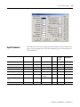
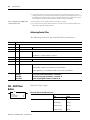
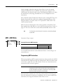
Summary of Changes
The information below summarizes the changes to this manual since the
last printing as publication 1763-RM001C-EN-P, October 2009.
To help you locate new and updated information in this release of the
manual, we have included change bars as shown to the right of this
paragraph.
Firmware Revision
History
Features are added to the controllers through firmware upgrades. See the
latest release notes, 1763-RN003, to be sure that your controller’s firmware
is at the level you need. Firmware upgrades are not required, except to
allow you access to the new features. See “Firmware Upgrades” below.
Firmware Upgrades
Enhanced features are added to the controllers through a firmware
upgrade. This firmware upgrade is not required, except to allow you access
to the latest features. To use the newest features, be sure your controller’s
firmware is at the following level:
Programmable
Controller
Firmware Revision
Catalog Numbers
MicroLogix 1100 Series B, Revision C, FRN 9 1763-L16AWA, 1763-L16BWA, 1763-L16BBB,
and 1763-L16DWD controllers
To upgrade the firmware for a MicroLogix controller visit the MicroLogix
web site at http://www.ab.com/micrologix.
To use all of the latest features, RSLogix 500 programming software must
be version 7.20.00 or higher.
3
Publication 1763-RM001D-EN-P - September 2011
4
Summary of Changes
Notes:
Publication 1763-RM001D-EN-P - September 2011
Table of Contents
Summary of Changes
Firmware Revision History . . . . . . . . . . . . . . . . . . . . . . . . . . . . . . . . . . . . 3
Firmware Upgrades . . . . . . . . . . . . . . . . . . . . . . . . . . . . . . . . . . . . . . . . . . 3
Table of Contents
Preface
Who Should Use this Manual. . . . . . . . . . . . . . . . . . . . . . . . . . . . . . . . . .
Purpose of this Manual. . . . . . . . . . . . . . . . . . . . . . . . . . . . . . . . . . . . . . .
Common Techniques Used in this Manual . . . . . . . . . . . . . . . . . . . . . . .
Related Documentation . . . . . . . . . . . . . . . . . . . . . . . . . . . . . . . . . . . . . .
Rockwell Automation Support . . . . . . . . . . . . . . . . . . . . . . . . . . . . . . . .
13
13
13
14
14
Chapter 1
I/O Configuration
Embedded I/O. . . . . . . . . . . . . . . . . . . . . . . . . . . . . . . . . . . . . . . . . . . . .
MicroLogix 1100 Expansion I/O . . . . . . . . . . . . . . . . . . . . . . . . . . . . . .
MicroLogix 1100 Expansion I/O Memory Mapping . . . . . . . . . . . . . . .
I/O Addressing. . . . . . . . . . . . . . . . . . . . . . . . . . . . . . . . . . . . . . . . . . . . .
I/O Forcing . . . . . . . . . . . . . . . . . . . . . . . . . . . . . . . . . . . . . . . . . . . . . . .
Input Filtering . . . . . . . . . . . . . . . . . . . . . . . . . . . . . . . . . . . . . . . . . . . . . .
Analog Inputs . . . . . . . . . . . . . . . . . . . . . . . . . . . . . . . . . . . . . . . . . . . . . .
Latching Inputs. . . . . . . . . . . . . . . . . . . . . . . . . . . . . . . . . . . . . . . . . . . . .
Configuring Expansion
I/O Using RSLogix 500 . . . . . . . . . . . . . . . . . . . . . . . . . . . . . . . . . . . . . .
15
17
17
26
27
27
28
30
34
Chapter 2
Controller Memory and File
Types
Controller Memory . . . . . . . . . . . . . . . . . . . . . . . . . . . . . . . . . . . . . . . . . .
Data Files . . . . . . . . . . . . . . . . . . . . . . . . . . . . . . . . . . . . . . . . . . . . . . . . .
Protecting Data Files During Download. . . . . . . . . . . . . . . . . . . . . . . . .
Static File Protection . . . . . . . . . . . . . . . . . . . . . . . . . . . . . . . . . . . . . . . .
Password Protection. . . . . . . . . . . . . . . . . . . . . . . . . . . . . . . . . . . . . . . . .
Clearing the Controller Memory . . . . . . . . . . . . . . . . . . . . . . . . . . . . . . .
Allow Future Access Setting (OEM Lock) . . . . . . . . . . . . . . . . . . . . . . .
Web View Disable (OS Series B FRN 4 or later) . . . . . . . . . . . . . . . . . .
36
40
42
44
45
46
47
47
Chapter 3
Function Files
Overview . . . . . . . . . . . . . . . . . . . . . . . . . . . . . . . . . . . . . . . . . . . . . . . . . .
Real-Time Clock Function File . . . . . . . . . . . . . . . . . . . . . . . . . . . . . . . .
RTA - Real Time Clock Adjust Instruction . . . . . . . . . . . . . . . . . . . . . .
Memory Module Information Function File. . . . . . . . . . . . . . . . . . . . . .
Base Hardware Information Function File . . . . . . . . . . . . . . . . . . . . . . .
Communications Status File. . . . . . . . . . . . . . . . . . . . . . . . . . . . . . . . . . .
Ethernet Communications Status File. . . . . . . . . . . . . . . . . . . . . . . . . . .
Input/Output Status File . . . . . . . . . . . . . . . . . . . . . . . . . . . . . . . . . . . . .
50
51
53
54
56
57
71
79
Chapter 4
Programming Instructions
Overview
5
Instruction Set. . . . . . . . . . . . . . . . . . . . . . . . . . . . . . . . . . . . . . . . . . . . . . 81
Using the Instruction Descriptions . . . . . . . . . . . . . . . . . . . . . . . . . . . . . 82
Publication 1763-RM001D-EN-P - September 2011
6
Table of Contents
Chapter 5
Using the High-Speed
Counter and Programmable
Limit Switch
High-Speed Counter Overview . . . . . . . . . . . . . . . . . . . . . . . . . . . . . . . . 89
Programmable Limit Switch Overview . . . . . . . . . . . . . . . . . . . . . . . . . . 89
High-Speed Counter (HSC) Function File . . . . . . . . . . . . . . . . . . . . . . . 90
High-Speed Counter Function File Sub-Elements Summary . . . . . . . . 92
HSC Function File Sub-Elements . . . . . . . . . . . . . . . . . . . . . . . . . . . . . . 93
HSL - High-Speed Counter Load . . . . . . . . . . . . . . . . . . . . . . . . . . . . . 118
RAC - Reset Accumulated Value. . . . . . . . . . . . . . . . . . . . . . . . . . . . . . 119
Programmable Limit Switch (PLS) File. . . . . . . . . . . . . . . . . . . . . . . . . 120
Chapter 6
Using High-Speed Outputs
PTO - Pulse Train Output. . . . . . . . . . . . . . . . . . . . . . . . . . . . . . . . . . .
Pulse Train Output Function. . . . . . . . . . . . . . . . . . . . . . . . . . . . . . . . .
Pulse Train Outputs (PTO) Function File . . . . . . . . . . . . . . . . . . . . . .
Pulse Train Output Function File Sub-Elements Summary . . . . . . . .
PWM - Pulse Width Modulation . . . . . . . . . . . . . . . . . . . . . . . . . . . . . .
PWM Function. . . . . . . . . . . . . . . . . . . . . . . . . . . . . . . . . . . . . . . . . . . .
Pulse Width Modulation (PWM) Function File . . . . . . . . . . . . . . . . . .
Pulse Width Modulated Function File Elements Summary . . . . . . . . .
127
128
133
134
149
149
150
152
Chapter 7
Relay-Type (Bit) Instructions
XIC - Examine if Closed
XIO - Examine if Open. . . . . . . . . . . . . . . . . . . . . . . . . . . . . . . . . . . . .
OTE - Output Energize. . . . . . . . . . . . . . . . . . . . . . . . . . . . . . . . . . . . .
OTL - Output Latch
OTU - Output Unlatch . . . . . . . . . . . . . . . . . . . . . . . . . . . . . . . . . . . . .
ONS - One Shot. . . . . . . . . . . . . . . . . . . . . . . . . . . . . . . . . . . . . . . . . . .
OSR - One Shot Rising
OSF - One Shot Falling . . . . . . . . . . . . . . . . . . . . . . . . . . . . . . . . . . . . .
159
161
162
163
164
Chapter 8
Timer and Counter
Instructions
Timer Instructions Overview . . . . . . . . . . . . . . . . . . . . . . . . . . . . . . . .
TON - Timer, On-Delay . . . . . . . . . . . . . . . . . . . . . . . . . . . . . . . . . . . .
TOF - Timer, Off-Delay . . . . . . . . . . . . . . . . . . . . . . . . . . . . . . . . . . . .
RTO - Retentive Timer, On-Delay . . . . . . . . . . . . . . . . . . . . . . . . . . . .
How Counters Work . . . . . . . . . . . . . . . . . . . . . . . . . . . . . . . . . . . . . . .
CTU - Count Up
CTD - Count Down. . . . . . . . . . . . . . . . . . . . . . . . . . . . . . . . . . . . . . . .
RES - Reset. . . . . . . . . . . . . . . . . . . . . . . . . . . . . . . . . . . . . . . . . . . . . . .
167
170
171
172
173
176
177
Chapter 9
Compare Instructions
Using the Compare Instructions . . . . . . . . . . . . . . . . . . . . . . . . . . . . . . 180
EQU - Equal
NEQ - Not Equal . . . . . . . . . . . . . . . . . . . . . . . . . . . . . . . . . . . . . . . . . 181
Publication 1763-RM001D-EN-P - September 2011
Table of Contents
GRT - Greater Than
LES - Less Than . . . . . . . . . . . . . . . . . . . . . . . . . . . . . . . . . . . . . . . . . .
GEQ - Greater Than or Equal To
LEQ - Less Than or Equal To . . . . . . . . . . . . . . . . . . . . . . . . . . . . . . .
MEQ - Mask Compare for Equal . . . . . . . . . . . . . . . . . . . . . . . . . . . . .
LIM - Limit Test . . . . . . . . . . . . . . . . . . . . . . . . . . . . . . . . . . . . . . . . . .
7
181
182
182
184
Chapter 10
Math Instructions
Using the Math Instructions . . . . . . . . . . . . . . . . . . . . . . . . . . . . . . . . .
Updates to Math Status Bits. . . . . . . . . . . . . . . . . . . . . . . . . . . . . . . . . .
Using the Floating Point (F) Data File . . . . . . . . . . . . . . . . . . . . . . . . .
ADD - Add
SUB - Subtract . . . . . . . . . . . . . . . . . . . . . . . . . . . . . . . . . . . . . . . . . . . .
MUL - Multiply
DIV - Divide . . . . . . . . . . . . . . . . . . . . . . . . . . . . . . . . . . . . . . . . . . . . .
NEG - Negate . . . . . . . . . . . . . . . . . . . . . . . . . . . . . . . . . . . . . . . . . . . .
CLR - Clear . . . . . . . . . . . . . . . . . . . . . . . . . . . . . . . . . . . . . . . . . . . . . .
ABS - Absolute Value . . . . . . . . . . . . . . . . . . . . . . . . . . . . . . . . . . . . . .
SCL - Scale . . . . . . . . . . . . . . . . . . . . . . . . . . . . . . . . . . . . . . . . . . . . . . .
SCP - Scale with Parameters . . . . . . . . . . . . . . . . . . . . . . . . . . . . . . . . .
SQR - Square Root . . . . . . . . . . . . . . . . . . . . . . . . . . . . . . . . . . . . . . . .
188
189
190
193
194
194
194
195
196
197
199
Chapter 11
Conversion Instructions
Using Decode and Encode Instructions . . . . . . . . . . . . . . . . . . . . . . . .
DCD - Decode 4 to 1-of-16 . . . . . . . . . . . . . . . . . . . . . . . . . . . . . . . . .
ENC - Encode
1-of-16 to 4 . . . . . . . . . . . . . . . . . . . . . . . . . . . . . . . . . . . . . . . . . . . . . .
FRD - Convert from Binary Coded Decimal (BCD) . . . . . . . . . . . . . .
TOD - Convert to Binary Coded Decimal (BCD) . . . . . . . . . . . . . . . .
GCD - Gray Code . . . . . . . . . . . . . . . . . . . . . . . . . . . . . . . . . . . . . . . . .
201
202
203
204
208
210
Chapter 12
Logical Instructions
Using Logical Instructions . . . . . . . . . . . . . . . . . . . . . . . . . . . . . . . . . . .
Updates to Math Status Bits. . . . . . . . . . . . . . . . . . . . . . . . . . . . . . . . . .
AND - Bit-Wise AND . . . . . . . . . . . . . . . . . . . . . . . . . . . . . . . . . . . . .
OR - Logical OR . . . . . . . . . . . . . . . . . . . . . . . . . . . . . . . . . . . . . . . . . .
XOR - Exclusive OR . . . . . . . . . . . . . . . . . . . . . . . . . . . . . . . . . . . . . . .
NOT - Logical NOT . . . . . . . . . . . . . . . . . . . . . . . . . . . . . . . . . . . . . . .
211
212
213
214
215
216
Chapter 13
Move Instructions
MOV - Move . . . . . . . . . . . . . . . . . . . . . . . . . . . . . . . . . . . . . . . . . . . . . 217
MVM - Masked Move . . . . . . . . . . . . . . . . . . . . . . . . . . . . . . . . . . . . . . 219
Chapter 14
File Instructions
CPW - Copy Word . . . . . . . . . . . . . . . . . . . . . . . . . . . . . . . . . . . . . . . . 222
Publication 1763-RM001D-EN-P - September 2011
8
Table of Contents
COP - Copy File . . . . . . . . . . . . . . . . . . . . . . . . . . . . . . . . . . . . . . . . . .
FLL - Fill File . . . . . . . . . . . . . . . . . . . . . . . . . . . . . . . . . . . . . . . . . . . .
BSL - Bit Shift Left . . . . . . . . . . . . . . . . . . . . . . . . . . . . . . . . . . . . . . . .
BSR - Bit Shift Right . . . . . . . . . . . . . . . . . . . . . . . . . . . . . . . . . . . . . . .
FFL - First In, First Out (FIFO) Load . . . . . . . . . . . . . . . . . . . . . . . . .
FFU - First In, First Out (FIFO) Unload . . . . . . . . . . . . . . . . . . . . . .
LFL - Last In, First Out (LIFO) Load . . . . . . . . . . . . . . . . . . . . . . . . .
LFU - Last In, First Out (LIFO) Unload . . . . . . . . . . . . . . . . . . . . . . .
SWP - Swap . . . . . . . . . . . . . . . . . . . . . . . . . . . . . . . . . . . . . . . . . . . . . .
223
225
226
228
230
232
234
236
238
Chapter 15
Sequencer Instructions
SQC- Sequencer Compare . . . . . . . . . . . . . . . . . . . . . . . . . . . . . . . . . . 240
SQO- Sequencer Output . . . . . . . . . . . . . . . . . . . . . . . . . . . . . . . . . . . 243
SQL - Sequencer Load . . . . . . . . . . . . . . . . . . . . . . . . . . . . . . . . . . . . . 246
Chapter 16
Program Control Instructions
JMP - Jump to Label . . . . . . . . . . . . . . . . . . . . . . . . . . . . . . . . . . . . . . .
LBL - Label . . . . . . . . . . . . . . . . . . . . . . . . . . . . . . . . . . . . . . . . . . . . . .
JSR - Jump to Subroutine . . . . . . . . . . . . . . . . . . . . . . . . . . . . . . . . . . .
SBR - Subroutine Label . . . . . . . . . . . . . . . . . . . . . . . . . . . . . . . . . . . . .
RET - Return from Subroutine . . . . . . . . . . . . . . . . . . . . . . . . . . . . . .
SUS - Suspend . . . . . . . . . . . . . . . . . . . . . . . . . . . . . . . . . . . . . . . . . . . .
TND - Temporary End . . . . . . . . . . . . . . . . . . . . . . . . . . . . . . . . . . . .
END - Program End . . . . . . . . . . . . . . . . . . . . . . . . . . . . . . . . . . . . . .
MCR - Master Control Reset . . . . . . . . . . . . . . . . . . . . . . . . . . . . . . . .
249
250
250
250
251
251
251
252
252
Chapter 17
Input and Output Instructions
IIM - Immediate Input with Mask . . . . . . . . . . . . . . . . . . . . . . . . . . . . 255
IOM - Immediate Output with Mask . . . . . . . . . . . . . . . . . . . . . . . . . . 257
REF- I/O Refresh . . . . . . . . . . . . . . . . . . . . . . . . . . . . . . . . . . . . . . . . . 258
Chapter 18
Using Interrupts
Information About Using Interrupts . . . . . . . . . . . . . . . . . . . . . . . . . .
User Interrupt Instructions . . . . . . . . . . . . . . . . . . . . . . . . . . . . . . . . . .
INT - Interrupt Subroutine . . . . . . . . . . . . . . . . . . . . . . . . . . . . . . . . .
STS - Selectable Timed Start . . . . . . . . . . . . . . . . . . . . . . . . . . . . . . . . .
UID - User Interrupt Disable . . . . . . . . . . . . . . . . . . . . . . . . . . . . . . . .
UIE - User Interrupt Enable . . . . . . . . . . . . . . . . . . . . . . . . . . . . . . . .
UIF - User Interrupt Flush . . . . . . . . . . . . . . . . . . . . . . . . . . . . . . . . . .
Using the Selectable Timed Interrupt (STI) Function File . . . . . . . . .
Using the Event Input Interrupt (EII) Function File. . . . . . . . . . . . . .
259
263
263
264
265
266
267
268
272
Chapter 19
Process Control Instruction
The PID Concept. . . . . . . . . . . . . . . . . . . . . . . . . . . . . . . . . . . . . . . . . . 279
The PID Equation . . . . . . . . . . . . . . . . . . . . . . . . . . . . . . . . . . . . . . . . . 280
Publication 1763-RM001D-EN-P - September 2011
Table of Contents
PD Data File . . . . . . . . . . . . . . . . . . . . . . . . . . . . . . . . . . . . . . . . . . . . . .
PID - Proportional Integral Derivative . . . . . . . . . . . . . . . . . . . . . . . .
Input Parameters . . . . . . . . . . . . . . . . . . . . . . . . . . . . . . . . . . . . . . . . . .
Output Parameters . . . . . . . . . . . . . . . . . . . . . . . . . . . . . . . . . . . . . . . . .
Tuning Parameters . . . . . . . . . . . . . . . . . . . . . . . . . . . . . . . . . . . . . . . . .
Runtime Errors . . . . . . . . . . . . . . . . . . . . . . . . . . . . . . . . . . . . . . . . . . . .
Analog I/O Scaling. . . . . . . . . . . . . . . . . . . . . . . . . . . . . . . . . . . . . . . . .
Application Notes. . . . . . . . . . . . . . . . . . . . . . . . . . . . . . . . . . . . . . . . . .
Application Examples . . . . . . . . . . . . . . . . . . . . . . . . . . . . . . . . . . . . . .
9
281
282
283
287
289
298
299
300
304
Chapter 20
ASCII Instructions
General Information. . . . . . . . . . . . . . . . . . . . . . . . . . . . . . . . . . . . . . . .
ASCII Instructions . . . . . . . . . . . . . . . . . . . . . . . . . . . . . . . . . . . . . . . . .
Instruction Types and Operation. . . . . . . . . . . . . . . . . . . . . . . . . . . . . .
Protocol Overview . . . . . . . . . . . . . . . . . . . . . . . . . . . . . . . . . . . . . . . . .
String (ST) Data File. . . . . . . . . . . . . . . . . . . . . . . . . . . . . . . . . . . . . . . .
Control Data File . . . . . . . . . . . . . . . . . . . . . . . . . . . . . . . . . . . . . . . . . .
ACL - ASCII Clear Buffers . . . . . . . . . . . . . . . . . . . . . . . . . . . . . . . . . .
AIC - ASCII Integer to String . . . . . . . . . . . . . . . . . . . . . . . . . . . . . . . .
AWA - ASCII Write with Append . . . . . . . . . . . . . . . . . . . . . . . . . . . .
AWT - ASCII Write . . . . . . . . . . . . . . . . . . . . . . . . . . . . . . . . . . . . . . .
ABL - Test Buffer for Line . . . . . . . . . . . . . . . . . . . . . . . . . . . . . . . . . .
ACB - Number of Characters in Buffer . . . . . . . . . . . . . . . . . . . . . . . .
ACI - String to Integer . . . . . . . . . . . . . . . . . . . . . . . . . . . . . . . . . . . . .
ACN - String Concatenate . . . . . . . . . . . . . . . . . . . . . . . . . . . . . . . . . .
AEX - String Extract . . . . . . . . . . . . . . . . . . . . . . . . . . . . . . . . . . . . . . .
AHL - ASCII Handshake Lines . . . . . . . . . . . . . . . . . . . . . . . . . . . . . .
ARD - ASCII Read Characters . . . . . . . . . . . . . . . . . . . . . . . . . . . . . . .
ARL - ASCII Read Line . . . . . . . . . . . . . . . . . . . . . . . . . . . . . . . . . . . .
ASC - String Search . . . . . . . . . . . . . . . . . . . . . . . . . . . . . . . . . . . . . . . .
ASR - ASCII String Compare . . . . . . . . . . . . . . . . . . . . . . . . . . . . . . . .
Timing Diagram for ARD, ARL, AWA, and AWT Instructions. . . . .
Using In-line Indirection . . . . . . . . . . . . . . . . . . . . . . . . . . . . . . . . . . . .
ASCII Instruction Error Codes . . . . . . . . . . . . . . . . . . . . . . . . . . . . . . .
ASCII Character Set . . . . . . . . . . . . . . . . . . . . . . . . . . . . . . . . . . . . . . . .
309
309
310
311
312
313
314
316
317
319
321
323
324
325
326
328
329
331
333
334
336
336
337
339
Chapter 21
Communications Instructions Messaging Overview. . . . . . . . . . . . . . . . . . . . . . . . . . . . . . . . . . . . . . . .
SVC - Service Communications . . . . . . . . . . . . . . . . . . . . . . . . . . . . . .
MSG - Message . . . . . . . . . . . . . . . . . . . . . . . . . . . . . . . . . . . . . . . . . . .
The Message Element . . . . . . . . . . . . . . . . . . . . . . . . . . . . . . . . . . . . . .
Timing Diagram for the MSG Instruction . . . . . . . . . . . . . . . . . . . . . .
Communication Servicing Selection and Message Servicing
Selection . . . . . . . . . . . . . . . . . . . . . . . . . . . . . . . . . . . . . . . . . . . . . . . . .
MSG Instruction Ladder Logic . . . . . . . . . . . . . . . . . . . . . . . . . . . . . . .
341
344
346
347
356
359
360
Publication 1763-RM001D-EN-P - September 2011
10
Table of Contents
Local Messages . . . . . . . . . . . . . . . . . . . . . . . . . . . . . . . . . . . . . . . . . . . . 361
Configuring a Local Message . . . . . . . . . . . . . . . . . . . . . . . . . . . . . . . . . 363
Local Messaging Examples . . . . . . . . . . . . . . . . . . . . . . . . . . . . . . . . . . 373
Remote Messages . . . . . . . . . . . . . . . . . . . . . . . . . . . . . . . . . . . . . . . . . . 388
Configuring a Remote Message . . . . . . . . . . . . . . . . . . . . . . . . . . . . . . . 391
Configuring a Multi-hop Remote Message on EtherNet/IP Communication
Channel . . . . . . . . . . . . . . . . . . . . . . . . . . . . . . . . . . . . . . . . . . . . . . . . . . 394
Configuring a MicroLogix 1100 CIP Generic Message via Ethernet (OS
Series B FRN 4 or later). . . . . . . . . . . . . . . . . . . . . . . . . . . . . . . . . . . . . 409
MSG Instruction Error Codes. . . . . . . . . . . . . . . . . . . . . . . . . . . . . . . . 414
Special Function with MSG instruction (OS Series B FRN 4 or
later) . . . . . . . . . . . . . . . . . . . . . . . . . . . . . . . . . . . . . . . . . . . . . . . . . . . . 416
Configure MSG Setup Screen to send SMTP message . . . . . . . . . . . . 422
Chapter 22
Recipe and Data Logging
RCP - Recipe . . . . . . . . . . . . . . . . . . . . . . . . . . . . . . . . . . . . . . . . . . . . .
Data Logging . . . . . . . . . . . . . . . . . . . . . . . . . . . . . . . . . . . . . . . . . . . . .
Queues and Records . . . . . . . . . . . . . . . . . . . . . . . . . . . . . . . . . . . . . . .
Configuring Data Log Queues. . . . . . . . . . . . . . . . . . . . . . . . . . . . . . . .
DLG - Data Log Instruction . . . . . . . . . . . . . . . . . . . . . . . . . . . . . . . .
Data Log Status File . . . . . . . . . . . . . . . . . . . . . . . . . . . . . . . . . . . . . . . .
Retrieving (Reading) Records . . . . . . . . . . . . . . . . . . . . . . . . . . . . . . . .
Accessing the Retrieval File . . . . . . . . . . . . . . . . . . . . . . . . . . . . . . . . . .
Conditions that Will Erase the Data Retrieval File. . . . . . . . . . . . . . . .
427
433
433
437
439
440
442
442
444
Chapter 23
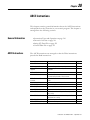
LCD Information
LCD Overview . . . . . . . . . . . . . . . . . . . . . . . . . . . . . . . . . . . . . . . . . . . .
LCD Function File . . . . . . . . . . . . . . . . . . . . . . . . . . . . . . . . . . . . . . . . .
LCD Function File Sub-Elements Summary . . . . . . . . . . . . . . . . . . . .
LCD Function File Sub-Elements. . . . . . . . . . . . . . . . . . . . . . . . . . . . .
LCD - LCD Instruction . . . . . . . . . . . . . . . . . . . . . . . . . . . . . . . . . . . .
445
446
447
448
453
Appendix A
MicroLogix 1100 Memory
Usage and Instruction
Execution Time
Programming Instructions Memory usage and Execution Time . . . . . 457
MicroLogix 1100
Scan Time Worksheet . . . . . . . . . . . . . . . . . . . . . . . . . . . . . . . . . . . . . . 462
Appendix B
System Status File
Status File Overview . . . . . . . . . . . . . . . . . . . . . . . . . . . . . . . . . . . . . . . 466
Status File Details . . . . . . . . . . . . . . . . . . . . . . . . . . . . . . . . . . . . . . . . . . 467
Appendix C
Fault Messages and Error
Codes
Identifying Controller Faults . . . . . . . . . . . . . . . . . . . . . . . . . . . . . . . . . 491
Contacting Rockwell Automation for Assistance . . . . . . . . . . . . . . . . . 499
Publication 1763-RM001D-EN-P - September 2011
Table of Contents
11
Appendix D
Protocol Configuration
DH-485 Communication Protocol . . . . . . . . . . . . . . . . . . . . . . . . . . .
DF1 Full-Duplex Protocol. . . . . . . . . . . . . . . . . . . . . . . . . . . . . . . . . . .
DF1 Half-Duplex Protocol . . . . . . . . . . . . . . . . . . . . . . . . . . . . . . . . . .
DF1 Radio Modem Protocol . . . . . . . . . . . . . . . . . . . . . . . . . . . . . . . . .
Modbus RTU Protocol. . . . . . . . . . . . . . . . . . . . . . . . . . . . . . . . . . . . . .
ASCII Driver . . . . . . . . . . . . . . . . . . . . . . . . . . . . . . . . . . . . . . . . . . . . .
Ethernet Driver. . . . . . . . . . . . . . . . . . . . . . . . . . . . . . . . . . . . . . . . . . . .
502
505
506
517
524
535
537
Appendix E
Knowledgebase Quick Starts # 17444 “Quick Start” Pulse Train Output (PTO) . . . . . . . . . . . . . . .
# 17446 “Quick Start” Pulse Width Modulation (PWM). . . . . . . . . . .
# 17447 “Quick Start” High Speed Counter (HSC). . . . . . . . . . . . . . .
# 17465 “Quick Start” Message (MSG) . . . . . . . . . . . . . . . . . . . . . . . .
# 17501 “Quick Start” Selectable Timed Interrupt (STI) . . . . . . . . . .
# 17503 “Quick Start” Real Time Clock (RTC) . . . . . . . . . . . . . . . . . .
# 17558 “Quick Start” User Interrupt Disable (UID) . . . . . . . . . . . . .
# 18465 “Quick Start” RTC Synchronization
Between Controllers . . . . . . . . . . . . . . . . . . . . . . . . . . . . . . . . . . . . . . . .
# 18498 “Quick Start” Data Logging (DLG) . . . . . . . . . . . . . . . . . . . .
541
544
546
550
553
556
557
558
561
Appendix F
How to Use 40kHz PTO/PWM
of MicroLogix 1100 Series B
Controller
Basic requirements to use 40KHz PTO and PWM in MicroLogix Controller
571
PTO and PWM function file changes in Series B Controller. . . . . . . . 571
RSLogix500 display issues . . . . . . . . . . . . . . . . . . . . . . . . . . . . . . . . . . . 572
Instruction issues . . . . . . . . . . . . . . . . . . . . . . . . . . . . . . . . . . . . . . . . . . 573
Appendix G
Number Systems
Binary Numbers . . . . . . . . . . . . . . . . . . . . . . . . . . . . . . . . . . . . . . . . . . . 581
Hexadecimal Numbers . . . . . . . . . . . . . . . . . . . . . . . . . . . . . . . . . . . . . . 583
Hex Mask . . . . . . . . . . . . . . . . . . . . . . . . . . . . . . . . . . . . . . . . . . . . . . . . 585
Appendix H
MicroLogix 1100 Firmware
System Related . . . . . . . . . . . . . . . . . . . . . . . . . . . . . . . . . . . . . . . . . . . .
Changes in OS Series B FRN 4 Serial Communications Related . . . . . . . . . . . . . . . . . . . . . . . . . . . . . . .
Ethernet Communications Related . . . . . . . . . . . . . . . . . . . . . . . . . . . .
Application Layer Related . . . . . . . . . . . . . . . . . . . . . . . . . . . . . . . . . . .
Embedded IO Configuration Related . . . . . . . . . . . . . . . . . . . . . . . . . .
Web-Server Related . . . . . . . . . . . . . . . . . . . . . . . . . . . . . . . . . . . . . . . .
RSLogix500 compatibility . . . . . . . . . . . . . . . . . . . . . . . . . . . . . . . . . . .
587
587
588
590
590
590
590
Glossary
Publication 1763-RM001D-EN-P - September 2011
12
Table of Contents
Index
MicroLogix 1100 List of Instructions and Function Files
Publication 1763-RM001D-EN-P - September 2011
Preface
Read this preface to familiarize yourself with the rest of the manual. It
provides information concerning:
• who should use this manual
• the purpose of this manual
• related documentation
• conventions used in this manual
• Rockwell Automation support
Who Should Use this
Manual
Use this manual if you are responsi3ble for designing, installing,
programming, or troubleshooting control systems that use MicroLogix
1100 controller.
You should have a basic understanding of electrical circuitry and
familiarity with relay logic. If you do not, obtain the proper training before
using this product.
Purpose of this Manual
This manual is a reference guide for MicroLogix 1100 controller. It
describes the procedures you use to program and troubleshoot your
controller. This manual:
• gives you an overview of the file types used by the controllers
• provides the instruction set for the controllers
• contains application examples to show the instruction set in use
Common Techniques
Used in this Manual
13
The following conventions are used throughout this manual:
• Bulleted lists such as this one provide information, not procedural
steps.
• Numbered lists provide sequential steps or hierarchical information.
• Change bars appear beside information that has been changed or
added since the last revision of this manual. Change bars appear in the
margin as shown to the right of this paragraph.
Publication 1763-RM001D-EN-P - September 2011
14
Preface
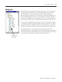
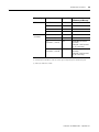
Related Documentation
The following documents contain additional information concerning
Rockwell Automation products. To obtain a copy, contact your local
Rockwell Automation office or distributor.
For
Read this Document
Information on understanding and applying micro controllers.
MicroMentor
Document Number
1761-MMB
Information on mounting and wiring the MicroLogix 1100 Programmable MicroLogix 1100 Programmable
Controller, including a mounting template and door labels.
Controllers Installation Instructions
1763-IN001
Detailed information on planning, mounting, wiring, and troubleshooting MicroLogix 1100 Programmable
your MicroLogix 1100 system.
Controllers User Manual
1763-UM001
A description on how to install and connect an AIC+. This manual also
contains information on network wiring.
Advanced Interface Converter (AIC+) User 1761-6.4
Manual
Information on how to install, configure, and commission a DNI
DeviceNet Interface User Manual
1761-6.5
Information on DF1 open protocol.
DF1 Protocol and Command Set
Reference Manual
1770-6.5.16
In-depth information on grounding and wiring Allen-Bradley
programmable controllers
Allen-Bradley Programmable Controller
Grounding and Wiring Guidelines
1770-4.1
A description of important differences between solid-state programmable Application Considerations for
controller products and hard-wired electromechanical devices
Solid-State Controls
SGI-1.1
An article on wire sizes and types for grounding electrical equipment
National Electrical Code - Published by the National Fire
Protection Association of Boston, MA.
A glossary of industrial automation terms and abbreviations
Allen-Bradley Industrial Automation
Glossary
AG-7.1
Before you contact Rockwell Automation for technical assistance, we
suggest you please review the troubleshooting information contained in
this publication first.
Rockwell Automation
Support
If the problem persists, call your local distributor or contact Rockwell
Automation in one of the following ways:
Phone
United States/Canada
1.440.646.3434
Outside United States/Canada
You can access the phone number for your country via the Internet:
1. Go to http://www.ab.com
2. Click on Product Support (http://support.automation.rockwell.com)
3. Under Support Centers, click on Contact Information
Internet
Publication 1763-RM001D-EN-P - September 2011
1. Go to http://www.ab.com
2. Click on Product Support (http://support.automation.rockwell.com)
Chapter
1
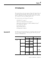
I/O Configuration
This section discusses the various aspects of Input and Output features of
the MicroLogix 1100 controllers. Each controller comes with a certain
amount of embedded I/O, which is physically located on the controller.
The controller also allows for adding expansion I/O.
This section discusses the following I/O functions:
• Embedded I/O on page 15
• MicroLogix 1100 Expansion I/O on page 17
• MicroLogix 1100 Expansion I/O Memory Mapping on page 17
• I/O Addressing on page 26
• I/O Forcing on page 27
• Input Filtering on page 27
• Latching Inputs on page 30
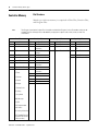
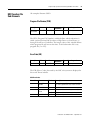
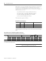
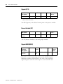
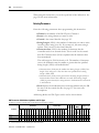
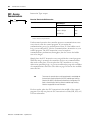
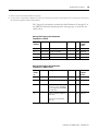
Embedded I/O
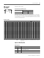
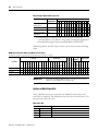
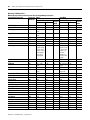
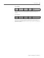
The MicroLogix 1100 provide discrete I/O and analog input that is built
into the controller as listed in the following table. These I/O points are
referred to as Embedded I/O.
Controller Family
MicroLogix 1100 1763-L16BWA
Controllers
1763-L16AWA
1763-L16BBB
Inputs
Quantity
Type
Quantity
Type
10
24V dc
discrete
6
relay
2
0~10V dc
analog
6
relay
10
120V ac
2
0~10V dc
analog
10
24V dc
2
relay
2
0~10V dc
analog
2
24V dc FET
2
high-speed
24V dc FET
6
relay
1763-L16DWD 10
2
15
Outputs
12/24Vdc
0~10V dc
analog
Publication 1763-RM001D-EN-P - September 2011
16
I/O Configuration
AC embedded inputs have fixed input filters. DC embedded inputs have
configurable input filters for a number of special functions that can be
used in your application. These are: high-speed counting, event input
interrupts, and latching inputs. The 1763-L16BBB has two high-speed
outputs for use as pulse train output (PTO) and/or pulse width
modulation (PWM) outputs.
Publication 1763-RM001D-EN-P - September 2011
I/O Configuration
MicroLogix 1100
Expansion I/O
17
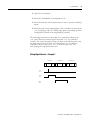
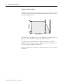
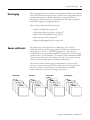
If the application requires more I/O than the controller provides, you can
attach I/O modules. These additional modules are called expansion I/O.
Expansion I/O Modules
For the MicroLogix 1100, Bulletin 1762 expansion I/O is used to provide
discrete and analog inputs and outputs, and specialty modules. You can
attach up to four expansion I/O modules in any combination.
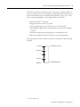
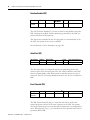
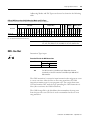
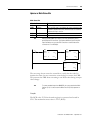
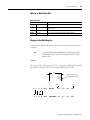
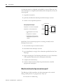
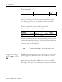
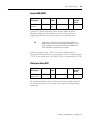
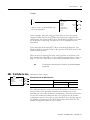
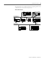
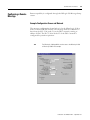
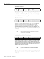
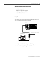
Addressing Expansion I/O Slots
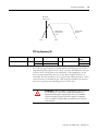
The figure below shows the addressing for the MicroLogix 1100 and its
I/O.
Slot 2
Embedded I/O = Slot 0
Slot 1
The expansion I/O is addressed as slots 1 through 4 (the controller’s
embedded I/O is addressed as slot 0). Modules are counted from left to
right as shown below.
Expansion I/O
TIP
In most cases, you can use the following address format:
X:s/b (X = file type letter, s = slot number, b = bit number)
See I/O Addressing on page 26 for complete information on address
formats.
MicroLogix 1100
Expansion I/O Memory
Mapping
Discrete I/O Configuration
1762-IA8 ,1762-IQ8, and 1762-IQ8OW6 Input Image
For each input module, the input data file contains the current state of the
field input points. Bit positions 0 through 7 correspond to input terminals
0 through 7.
Publication 1763-RM001D-EN-P - September 2011
I/O Configuration
Word
18
0
Bit Position
15 14 13
x
x
x
12
x
11
x
10
x
9
x
8
x
7
r
6
r
5
r
4
r
3
r
2
r
1
r
0
r
r = read only, x = not used, always at a 0 or OFF state
1762-IQ16 Input Image
Word
For each input module, the input data file contains the current state of the
field input points. Bit positions 0 through 15 correspond to input
terminals 0 through 15.
Bit Position
15
14
13
12
11
10
9
8
7
6
5
4
3
2
1
0
0
r
r
r
r
r
r
r
r
r
r
r
r
r
r
r
r
r = read only
1762-IQ32T Input Image
Word
For each input module, the input data file contains the current state of the
field input points. Bit positions 0…15 together with word 0/1 correspond
to input terminals 0…31.
Bit Position
15
14
13
12
11
10
9
8
7
6
5
4
3
2
1
0
0
r
r
r
r
r
r
r
r
r
r
r
r
r
r
r
r
1
r
r
r
r
r
r
r
r
r
r
r
r
r
r
r
r
r = read only
1762-OX6I and 1762-IQ8OW6 Output Image
Word
For each output module, the output data file contains the
controller-directed state of the discrete output points. Bit positions 0
through 5 correspond to output terminals 0 through 5.
Bit Position
15
14
13
12
11
10
9
8
7
6
5
0
0
0
0
0
0
0
0
0
0
0
r/w r/w r/w r/w r/w r/w
r/w = read and write, 0 = always at a 0 or OFF state
Publication 1763-RM001D-EN-P - September 2011
4
3
2
1
0
I/O Configuration
19
1762-OA8, 1762-OB8, and 1762-OW8 Output Image
Word
For each output module, the output data file contains the
controller-directed state of the discrete output points. Bit positions 0
through 7 correspond to output terminals 0 through 7.
Bit Position
15
14
13
12
11
10
9
8
7
0
0
0
0
0
0
0
0
0
r/w r/w r/w r/w r/w r/w r/w r/w
6
5
4
3
2
1
0
r/w = read and write, 0 = always at a 0 or OFF state
1762-OB16 and 1762-OW16 Output Image
Word
For each output module, the output data file contains the
controller-directed state of the discrete output points. Bit positions 0
through 15 correspond to output terminals 0 through 15.
Bit Position
0
r/w r/w r/w r/w r/w r/w r/w r/w r/w r/w r/w r/w r/w r/w r/w r/w
15
14
13
12
11
10
9
8
7
6
5
4
3
2
1
0
r/w = read and write
1762-OV32T, 1762-OB32T Output Image
Word
For each output module, the output data file contains the
controller-directed state of the discrete output points. Bit positions 0…15
together with word 0/1 correspond to output terminals 0…31.
Bit Position
0
r/w r/w r/w r/w r/w r/w r/w r/w r/w r/w r/w r/w r/w r/w r/w r/w
1
r/w r/w r/w r/w r/w r/w r/w r/w r/w r/w r/w r/w r/w r/w r/w r/w
15
14
13
12
11
10
9
8
7
6
5
4
3
2
1
0
r/w = read and write
Publication 1763-RM001D-EN-P - September 2011
20
I/O Configuration
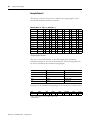
Analog I/O Configuration
The following table shows the data ranges for 0 to 10V dc and 4 to 20
mA.
Valid Input/Output Data Word Formats/Ranges
Normal Operating Range Full Scale Range Raw/Proportional Data
Scaled-for-PID
0 to 10V dc
4 to 20 mA
10.5V dc
32,760
16,380
0.0V dc
0
0
21.0 mA
32,760
16,380
20.0 mA
31,200
15,600
4.0 mA
6240
3120
0.0 mA
0
0
1762-IF2OF2 Input Data File
For each input module, slot x, words 0 and 1 contain the analog values of
the inputs. The module can be configured to use either raw/proportional
data or scaled-for-PID data. The input data file for each configuration is
shown below.
Word
Raw/Proportional Format
Bit Position
15 14 13
0
1
2
3
4
5
0
Channel 0 Data 0 to 32,768
0
Channel 1 Data 0 to 32,768
reserved
reserved
reserved
U0 O0 U1 O1 reserved
12
11
10
9
8
7
6
5
4
3
2
1
0
0
0
0
0
0
0
S1
S0
1
0
0
0
0
0
S1
S0
Word
Scaled-for-PID Format
Bit Position
15 14 13
0
1
2
3
4
5
0
0
0
0
reserved
reserved
reserved
U0 O0
12
11
10
9
Channel 0 Data 0 to 16,383
Channel 1 Data 0 to 16,383
U1
O1
8
7
6
5
4
3
2
reserved
The bits are defined as follows:
• Sx = General status bits for channels 0 and 1. This bit is set when an
error (over- or under-range) exists for that channel, or there is a
general module hardware error.
Publication 1763-RM001D-EN-P - September 2011
I/O Configuration
21
• Ox = Over-range flag bits for channels 0 and 1. These bits can be
used in the control program for error detection.
• Ux = Under-range flag bits for channels 0 and 1. These bits can be
used in the control program for error detection.
1762-IF2OF2 Output Data File
For each module, slot x, words 0 and 1 contain the channel output data.
Word
Raw/Proportional Format
Bit Position
15
14
0
0
1
0
13
12
11
10
9
8
7
6
5
4
3
2
1
0
Channel 0 Data 0 to 32,768
0
0
0
Channel 1 Data 0 to 32,768
0
0
0
Word
Scaled-for-PID Format
Bit Position
15
14
13
1
0
0
0
0
Channel 0 Data 0 to 16,383
0
0
1
0
0
Channel 1 Data 0 to 16,383
0
0
12
11
10
9
8
7
6
5
4
3
2
1762-IF4 Input Data File
For each module, slot x, words 0 and 1 contain the analog values of the
inputs. The module can be configured to use either raw/proportional data
or scaled-for-PID data. The input data file for either configuration is
shown below.
Word
1762-IF4 Input Data File
0
1
2
3
4
5
6
Bit Position
15
14 13 12 11
SGN0 Channel 0 Data
SGN1 Channel 1 Data
SGN2 Channel 2 Data
SGN3 Channel 3 Data
reserved
U0
O0 U1 O1 U2
reserved
10
9
8
7
6
O2
U3
O3
reserved
5
4
3
2
1
0
S3
S2
S1
S0
The bits are defined as follows:
Publication 1763-RM001D-EN-P - September 2011
22
I/O Configuration
• Sx = General status bits for channels 0 through 3. This bit is set when an error
(over- or under-range) exists for that channel, or there is a general module
hardware error.
• Ox = Over-range flag bits for channels 0 through 3. These bits are set when the
input signal is above the user-specified range. The module continues to convert
data to the maximum full range value during an over-range condition. The bits
reset when the over-range condition clears.
• UIx = Under-range flag bits for input channels 0 through 3. These bits are set
when the input signal is below the user-specified range. The module continues
to convert data to the maximum full range value during an under-range
condition. The bits reset when the under-range condition clears.
• SGNx = The sign bit for channels 0 through 3.
1762-OF4 Input Data File
For each module, slot x, words 0 and 1 contain the analog output module
status data for use in the control program.
Word
1762-OF4 Input Data File
Bit Position
15 14 13 12 11 10 9
8
7
6
5
4
3
2
1
0
0 Reserved
SO3 SO2 SO1 SO0
1 Reserved
UO0 OO0 UO1 OO1 UO2 OO2 UO3 OO3
The bits are defined as follows:
• SOx = General status bits for output channels 0 through 3. This bit is
set when an error (over- or under-range) exists for that channel, or
there is a general module hardware error.
• OOx = Over-range flag bits for output channels 0 through 3. These
bits indicate an input signal above the user range and can be used in
the control program for error detection. The module continues to
convert analog data to the maximum full range value while this bit is
set (1). The bit is reset (0) when the error clears.
• UOx = Under-range flag bits for output channels 0 through 3. These
bits indicate an input signal below the user range. They can be used in
the control program for error detection. The module continues to
convert analog data to the minimum full range value while this bit is
set (1). The bit is reset (0) when the error clears.
Publication 1763-RM001D-EN-P - September 2011
I/O Configuration
23
1762-OF4 Output Data File
For each module, slot x, words 0 through 3 contain the channel output
data.
Word
Raw/Proportional Format
Bit Position
15
14
0
0
1
0
2
3
13
12
11
10
9
8
7
6
5
4
3
2
1
0
Channel 0 Data 0 to 32,760
0
0
0
Channel 1 Data 0 to 32,760
0
0
0
0
Channel 2 Data 0 to 32,760
0
0
0
0
Channel 3 Data 0 to 32,760
0
0
0
Words 0 through 3 contain the analog output data for channels 0 through
3, respectively. The module ignores the “don’t care” bits (0 through 2), but
checks the sign bit (15). If bit 15 equals 1, the module sets the output
value to 0V or 0 mA.
Word
Scaled-for-PID Format
Bit Position
15
14
13
1
0
0
0
0
Channel 0 Data 0 to 16,380
0
0
1
0
0
Channel 1 Data 0 to 16,380
0
0
2
0
0
Channel 2 Data 0 to 16,380
0
0
3
0
0
Channel 3 Data 0 to 16,380
0
0
12
11
10
9
8
7
6
5
4
3
2
Words 0 through 3 contain the analog output data for channels 0 through
3, respectively. The module ignores the “don’t care” bits (0 and 1), but
checks the sign bit (15), and bit 14. If bit 15 equals 1, the module sets the
output value to 0V or 0 mA. If bit 15 equals zero and bit 14 equals 1, the
module sets the output value to 10.5V dc or 21 mA.
Publication 1763-RM001D-EN-P - September 2011
24
I/O Configuration
Specialty I/O Configuration
1762-IR4 RTD/resistance Module Input Data File
For each module, slot x, words 0 through 3 contain the analog values of
the inputs. Words 4 and 5 provide sensor/channel status feedback. The
input data file for each configuration is shown below.
Word 15
/Bit
14
13
12
11
10
0
Analog Input Data Channel 0
1
Analog Input Data Channel 1
2
Analog Input Data Channel 2
3
Analog Input Data Channel 3
4
Reserved
5
U0 O0
9
8
7
6
OC3 OC2 OC1 OC0 Reserved
U1 O1
U2
O2
U3
O3
5
4
3
2
1
0
S3
S2
S1
S0
Reserved
The bits are defined as follows:
• Sx = General status bits for input channels 0 through 3. This bit is set
(1) when an error (over- or under-range, open-circuit or input data not
valid condition) exists for that channel, or there is a general module
hardware error. An input data not valid condition is determined by the
user program. See MicroLogix 1200 RTD/Resistance Input Module
User Manual, publication 1762-UM003, for details.
• OCx = Open-circuit indication for channels 0 through 3, using either
RTD or resistance inputs. Short-circuit detection for RTD inputs only.
Short-circuit detection for resistance inputs is not indicated because 0
is a valid number.
• Ox = Over-range flag bits for input channels 0 through 3, using either
RTD or resistance inputs. These bits can be used in the control
program for error detection.
• Ux = Under-range flag bits for channels 0 through 3, using RTD
inputs only.
These bits can be used in the control program for error detection.
Under-range detection for direct resistance inputs is not indicated
because 0 is a valid number.
Publication 1763-RM001D-EN-P - September 2011
I/O Configuration
25
1762-IT4 Thermocouple Module Input Data File
For each module, slot x, words 0 through 3 contain the analog values of
the inputs. The input data file is shown below.
14
0
Analog Input Data Channel 0
1
2
3
SGN SGN SGN SGN
Word/ 15
Bit
13
12
11
10
9
8
7
6
5
4
3
2
1
0
Analog Input Data Channel 1
Analog Input Data Channel 2
Analog Input Data Channel 3
4
Reserved
5
U0 O0
OC4 OC3 OC2 OC1 OC0 Reserved
U1
O1
U2
O2
U3
O3
S4 S3 S2 S1 S0
U4 O4 Reserved
The bits are defined as follows:
• Sx = General status bits for channels 0 through 3 (S0 through S3) and
the CJC sensor (S4). This bit is set (1) when an error (over-range,
under-range, open-circuit, or input data not valid) exists for that
channel. An input data not valid condition is determined by the user
program. Refer to MicroLogix 1200 I/O Thermocouple/mV Input
Module User Manual, publication 1762-UM002 for additional details.
• OCx = Open-circuit indication for channels 0 through 3 (OC0
through OC3) and the CJC sensor (OC4).
• Ox = Over-range flag bits for channels 0 through 3 (O0 through O3)
and the CJC sensor (O4). These bits can be used in the control
program for error detection.
• Ux = Under-range flag bits for channels 0 through 3 (U0 through U3)
and the CJC sensor (U4). These bits can be used in the control
program for error detection.
Publication 1763-RM001D-EN-P - September 2011
26
I/O Configuration
I/O Addressing
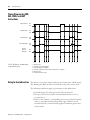
Addressing Details
The I/O addressing scheme and examples are shown below.
Slot Number (1)
Word
Data File Number
File Type
Input (I) or Output (O)
Xd:s.w/b
Slot Delimiter
Word Delimiter
Bit
Bit Delimiter
(1) I/O located on the controller (embedded I/O) is slot 0.
I/O added to the controller (expansion I/O) begins with slot 1.
Format
Explanation
Od:s.w/b X
File Type
Input (I) or Output (O)
d
Data File Number (optional)
0 = output, 1 = input
Id:s.w/b :
Slot delimiter (optional, not required for Data Files 2 to 255)
s
Slot number (decimal)
Embedded I/O: slot 0
Expansion I/O:
.
w
• slots 1 to 4 for MicroLogix 1100 (See page 17 for an illustration.)
Word delimiter. Required only if a word number is necessary as noted below.
Word number
Required to read/write words, or if the discrete bit number is above 15.
/
b
Bit delimiter
Bit number
Range: 0 to 255
0 to 15
Addressing Examples
Addressing Level
Example Address(1)
Slot
Word
Bit
Bit Addressing
O:0/4(2)
Output Slot 0 (Embedded I/O)
word 0
output bit 4
O:2/7(2)
Output Slot 2 (Expansion I/O)
word 0
output bit 7
I:1/4(2)
Input Slot 1 (Expansion I/O)
word 0
input bit 4
I:0/15(2)
O:1.0
I:7.3
I:3.1
Input Slot 0 (Embedded I/O)
word 0
input bit 15
Output Slot 1 (Expansion I/O)
Input Slot 7 (Expansion I/O)
Input Slot 3 (Expansion I/O)
word 0
word 3
word 1
Word Addressing
(1) The optional Data File Number is not shown in these examples.
(2) A word delimiter and number are not shown. Therefore, the address refers to word 0.
Publication 1763-RM001D-EN-P - September 2011
I/O Configuration
I/O Forcing
27
I/O forcing is the ability to override the actual status of the I/O at the
user’s discretion.
Input Forcing
When an input is forced, the value in the input data file is set to a
user-defined state. For discrete inputs, you can force an input “on” or
“off ”. When an input is forced, it no longer reflects the state of the
physical input or the input LCD indicator. For embedded inputs, the
controller reacts as if the force is applied to the physical input terminal.
TIP
When an input is forced, it has no effect on the input device connected
to the controller.
Output Forcing
When an output is forced, the controller overrides the status of the
control program, and sets the output to the user-defined state. Discrete
outputs can be forced “on” or “off ”. The value in the output file is
unaffected by the force. It maintains the state determined by the logic in
the control program. However, the state of the physical output and the
output LCD indicator will be set to the forced state.
TIP
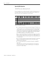
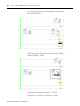
Input Filtering
If you force an output controlled by an executing PTO or PWM function,
an instruction error is generated.
The MicroLogix 1100 controllers allow users to configure groups of DC
inputs for high-speed or normal operation. Users can configure each
input group’s response time. A configurable filter determines how long
the input signal must be “on” or “off ” before the controller recognizes
the signal. The higher the value, the longer it takes for the input state to be
recognized by the controller. Higher values provide more filtering, and are
used in electrically noisy environments. Lower values provide less filtering,
and are used to detect fast or narrow pulses. You typically set the filters to
a lower value when using high-speed counters, latching inputs, and input
interrupts.
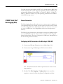
Input filtering is configured using RSLogix 500 programming software.
To configure the filters using RSLogix 500:
Publication 1763-RM001D-EN-P - September 2011
28
I/O Configuration
1. Open the “Controller” folder.
2. Open the “I/O Configuration” folder.
3. Open slot 0 (controller).
4. Select the “embedded I/O configuration” tab.
The input groups are pre-arranged. Simply select the filter time you
require for each input group. You can apply a unique input filter setting to
each of the input groups:
Controller
MicroLogix 1100
Input Groups
• 0 and 1
• 2 and 3
• 4 and 5
• 6 and 7
• 8 and above
The minimum and maximum response times associated with each input
filter setting can be found in your controller’s User Manual.
Analog Inputs
The MicroLogix 1100 has two 10-bit resolution analog input channels.
These channels are single-ended(unipolar) circuits and accept 0-10V dc.
Input words 4-5 contain the value of analog inputs(Word 4 : analog input
channel 0, Word 5 : analog input channel 1).
Analog Input Filter and Update times
The MicroLogix 1100 analog input filter is programmable. The slower the
filter setting, the more immune the analog inputs are to electrical noise.
The more immune the analog inputs are to electrical noise, the slower the
inputs will be to update. Similarly, the faster the filter setting, the less
immune the analog inputs are to electrical noise. The less immune the
analog inputs are to electrical noise, the faster the inputs will be to update.
Publication 1763-RM001D-EN-P - September 2011
I/O Configuration
29
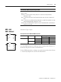
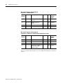
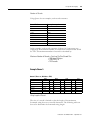
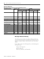
Programmable Filter Characteristics
1st Notch Freq (Hz)
Filter Bandwidth (-3 Settling Time
dB Freq Hz)
(mSec)
Resolution (Bits)
10
2.62
100.00
10
50
13.10
20.00
10
60
15.72
16.67
10
250
65.50
4
10
TIP
• 10 Hz is the default setting
• The total update time is one ladder scan time plus the settling time.
EXAMPLE
If a 250 Hz filter is selected, the maximum update Time = ladder
scan time + 4ms
Input Channel Filtering
The analog input channels incorporate on-board signal conditioning, to
distinguish AC power line noise from normal variations in the input
signal. Frequency components of the input signal at the filter frequency
are rejected. Frequency components below the filter bandwidth (-3 dB
frequency) are passed with under 3 dB of attenuation. This pass band
allows the normal variation of sensor inputs such as temperature, pressure
and flow transducers to be input data to the processor. Noise signals
coupled in at frequencies above the pass band are sharply rejected. An
area of particular concern is the 50/60 Hz region, where pick-up from
power lines can occur.
Converting Analog Data
The analog input circuits are able to monitor voltage signals and convert
them to digital data. There are three terminals assigned to the input
channels that provide two voltage inputs, and a return signal (commons).
Publication 1763-RM001D-EN-P - September 2011
30
I/O Configuration
The following table shows sample Analog Signal and Data Word values
using the nominal transfer function formula:
N=Vin x 1023/10 where Vin (analog signal) is in volts (V)
Analog Signal
Data Word
0V
0
5V
512
10V
1023
Converting Analog Input Data
Analog inputs convert voltage signals into 10-bit values. To determine an
approximate voltage that an input value represents, use the equations
shown below.
10V----------× inputvalue = inputvoltage ( V )
1023
For example, if an input value of 300 is in the input image, the calculated
value is:
10V----------× 300 = 2.9326 ( V )
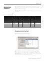
1023
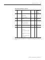
Latching Inputs
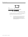
The MicroLogix 1100 controller provides the ability to individually
configure inputs to be latching inputs (sometimes referred to as pulse
catching inputs). A latching input is an input that captures a very fast
pulse and holds it for a single controller scan. The pulse width that can be
captured is dependent upon the input filtering selected for that input.
The following inputs can be configured as latching inputs:
Controller
MicroLogix 1100
DC Inputs
0 through 3
You enable this feature with RSLogix 500 programming software. With an
open project:
1. Open the “Controller” folder.
2. Open the “I/O Configuration” folder.
Publication 1763-RM001D-EN-P - September 2011
I/O Configuration
31
3. Open slot 0 (controller).
4. Select the “embedded I/O configuration” tab.
5. Select the mask bits for the inputs that you want to operate as latching
inputs.
6. Select the state for the latching inputs. The controller can detect both
“on” (rising edge) and “off ” (falling edge) pulses, depending upon the
configuration selected in the programming software.
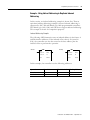
The following information is provided for a controller looking for an
“on” pulse. When an external signal is detected “on”, the controller
“latches” this event. In general, at the next input scan following this event,
the input image point is turned “on” and remains “on” for the next
controller scan. It is then set to “off ” at the next input scan. The
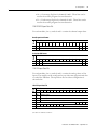
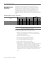
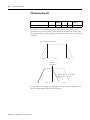
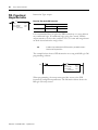
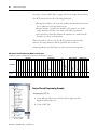
following figures help demonstrate this.
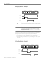
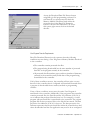
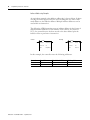
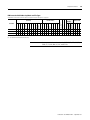
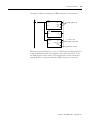
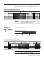
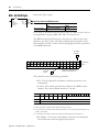
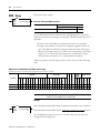
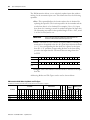
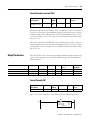
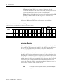
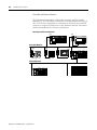
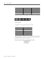
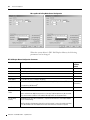
Rising Edge Behavior - Example 1
Scan Number (X)
Input
Scan
Ladder
Scan
Output
Scan
Scan Number (X+1)
Input
Scan
Ladder
Scan
Output
Scan
Scan Number (X+2)
Input
Scan
Ladder
Scan
Output
Scan
External
Input
Latched
Status
Input File
Value
Publication 1763-RM001D-EN-P - September 2011
32
I/O Configuration
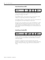
Rising Edge Behavior - Example 2
Scan Number (X)
Input
Scan
Ladder
Scan
Scan Number (X+1)
Output
Scan
Input
Scan
Ladder
Scan
Output
Scan
Scan Number (X+2)
Input
Scan
Ladder
Scan
Output
Scan
External
Input
Latched
Status
Input File
Value
TIP
The “gray” area of the Latched Status waveform is the input filter delay.
IMPORTANT
The input file value does not represent the external input when the input
is configured for latching behavior. When configured for rising edge
behavior, the input file value is normally “off” (“on” for 1 scan when a
rising edge pulse is detected).
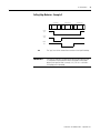
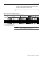
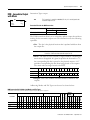
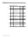
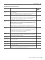
The previous examples demonstrate rising edge behavior. Falling edge
behavior operates exactly the same way with these exceptions:
• The detection is on the “falling edge” of the external input.
• The input image is normally “on” (1), and changes to “off ” (0) for
one scan.
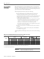
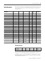
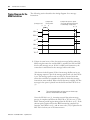
Falling Edge Behavior - Example 1
Scan Number (X)
Input
Scan
External
Input
Latched
Status
Input File
Value
Publication 1763-RM001D-EN-P - September 2011
Ladder Output
Scan Scan
Scan Number (X+1)
Input
Scan
Ladder Output
Scan Scan
Scan Number (X+2)
Input
Scan
Ladder Output
Scan Scan
Scan Number (X+3)
Input
Scan
Ladder Output
Scan Scan
I/O Configuration
33
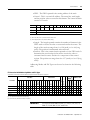
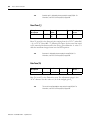
Falling Edge Behavior - Example 2
Scan Number (X)
Input
Scan
Ladder
Scan
Output
Scan
Scan Number (X+1)
Input
Scan
Ladder
Scan
Output
Scan
Scan Number (X+2)
Input
Scan
Ladder
Scan
Output
Scan
External
Input
Latched
Status
Input File
Value
TIP
The “gray” area of the Latched Status waveform is the input filter delay.
IMPORTANT
The input file value does not represent the external input when the input
is configured for latching behavior. When configured for falling edge
behavior, the input file value is normally “on” (“off” for 1 scan when a
falling edge pulse is detected).
Publication 1763-RM001D-EN-P - September 2011
34
I/O Configuration
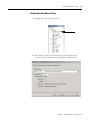
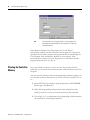
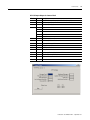
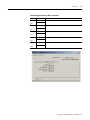
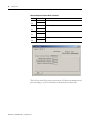
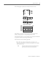
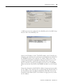
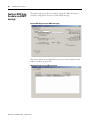
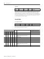
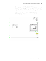
Configuring Expansion
I/O Using RSLogix 500
Expansion I/O must be configured for use with the controller.
Configuring expansion I/O can be done either manually, or automatically.
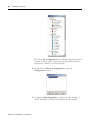
Using RSLogix 500:
1. Open the “Controller” folder.
2. Open the “I/O Configuration” folder.
3. For manual configuration, drag the Compact I/O module to the slot.
For automatic configuration, you must have the controller connected
online to the computer (either directly or over a network). Click the
“Read I/O Config” button on the I/O configuration screen. RSLogix
500 will read the existing configuration of the controller’s I/O.
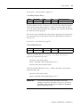
Some I/O modules support or require configuration. To configure a
specific module, double-click on the module, an I/O configuration screen
will open that is specific to the module.
Publication 1763-RM001D-EN-P - September 2011
Chapter
2
Controller Memory and File Types
This chapter describes controller memory and the types of files used by
the MicroLogix 1100 controller. The chapter is organized as follows:
• Controller Memory on page 36
• Data Files on page 40
• Protecting Data Files During Download on page 42
• Static File Protection on page 44
• Password Protection on page 45
• Clearing the Controller Memory on page 46
• Allow Future Access Setting (OEM Lock) on page 47
• Web View Disable (OS Series B FRN 4 or later) on page 47
35
Publication 1763-RM001D-EN-P - September 2011
36
Controller Memory and File Types
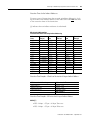
Controller Memory
File Structure
MicroLogix 1100 user memory is comprised of Data Files, Function Files,
and Program Files.
The file types shown below for data files 3 through 8 are the default file types for those file numbers and cannot be
changed. Data files 9 through 255 can be added to your program to operate as bit, timer, counter, or other files
shown below.
TIP
Data Files
Function Files
Program Files
Specialty Files
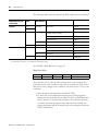
0
Output File
HSC
High Speed Counter
0
System File 0
0
Data Log Queue 0
1
Input File
PTO
Pulse Train Output
1
System File 1
1
Data Log Queue 1
2
Status File
PWM
Pulse Width
Modulation
2
Program File 2
2 to 255 Data Log Queues 2 to
255
3
Bit File
STI
Selectable Timed
Interrupt
3 to 255 Program Files 3 to 255 0
Recipe File 0
4
Timer File
EII
Event Input Interrupt
1
Recipe File 1
5
Counter File
RTC
Real Time Clock
2 to 255 Recipe Files 2 to 255
6
Control File
7
Integer File
MMI
Memory Module
Information
8
Floating Point File
BHI
Base Hardware
Information
(T) Timer
CS
Communications Status
(C) Counter
IOS
I/O Status
9 to 255 (B) Bit
DLS
Data Log Status
(R) Control
LCD
LCD
(N) Integer
ES
Ethernet Status
(F) Floating Point
(ST) String
(L) Long Word
(MG) Message
(PD) PID
(PLS) Programmable
Limit Switch
(RI) Routing Information
(RIX) Extended Routing
Information (OS Series
B FRN 4 or later)
Publication 1763-RM001D-EN-P - September 2011
Controller Memory and File Types
37
User Memory
User memory is the amount of storage available to a user for storing
ladder logic, data table files, I/O configuration, etc., in the controller.
User data files consist of the system status file, I/O image files, and all
other user-creatable data files (bit, timer, counter, control, integer, string,
long word, MSG, and PID).
A word is defined as a unit of memory in the controller. The amount of
memory available to the user for data files and program files is measured
in user words. Memory consumption is allocated as follows:
• For data files, a word is the equivalent of 16 bits of memory. For
example,
– 1 integer data file element = 1 user word
– 1 long word file element = 2 user words
– 1 timer data file element = 3 user words
TIP
Each input and output data element consumes 3 user words
due to the overhead associated with I/O forcing.
• For program files, a word is the equivalent of a ladder instruction with
one operand. For example(1),
– 1 XIC instruction, which has 1 operand, consumes 1 user word
– 1 EQU instruction, which has 2 operands, consumes 2 user words
– 1 ADD instruction, which has 3 operands, consumes 3 user words
• Function files do not consume user memory.
TIP
Although the controller allows up to 256 elements in a file, it may not
actually be possible to create a file with that many elements due to the
user memory size in the controller.
(1) These are approximate values. For actual memory usage, see the tables in Appendix A of this manual.
Publication 1763-RM001D-EN-P - September 2011
38
Controller Memory and File Types
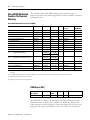
MicroLogix 1100 User Memory
The MicroLogix 1100 controller supports 8K of memory. Memory can be
used for program files and data files. The maximum data memory usage is
4K words as shown below.
Data Words
4.0K
0.5K
0K
0K
Program Words
4.0K
4.7K
See MicroLogix 1100 Memory Usage and Instruction Execution Time on
page 457 to find the memory usage for specific instructions.
The MicroLogix 1100 controller also supports 64K bytes of battery
backed memory for Data Logging or Recipe operations. See Chapter 22
for Data Logging and Recipe information.
See System Status File on page 465 to find the memory usage for specific
instructions.
Publication 1763-RM001D-EN-P - September 2011
Controller Memory and File Types
39
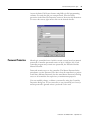
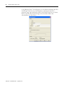
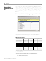
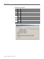
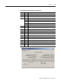
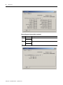
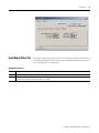
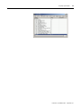
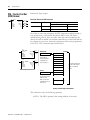
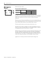
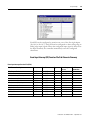
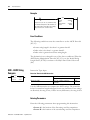
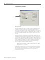
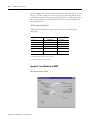
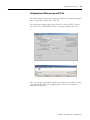
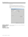
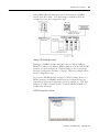
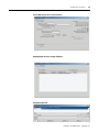
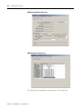
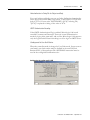
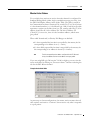
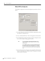
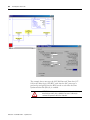
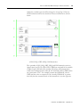
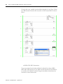
Viewing Controller Memory Usage
1. Highlight and open Controller Properties.
2. The amount of Memory Used and Memory Left will appear in the
Controller Properties window once the program has been verified.
Publication 1763-RM001D-EN-P - September 2011
40
Controller Memory and File Types
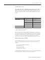
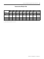
Data files store numeric information, including I/O, status, and other data
associated with the instructions used in ladder subroutines. The data file
types are:
Data Files
File Name
File
Identifier
File
Number(2)
Words per
Element
File Description
Output File
O
0
1
The Output File stores the values that are written to the physical outputs
during the Output Scan.
Input File
I
1
1
The Input File stores the values that are read from the physical inputs
during the Input Scan.
Status File
S
2
1
The contents of the Status File are determined by the functions which
utilize the Status File. See System Status File on page 465 for a detailed
description.
Bit File
B
3, 9 to 255
1
The Bit File is a general purpose file typically used for bit logic.
Timer File
T
4, 9 to 255
3
The Timer File is used for maintaining timing information for ladder logic
timing instructions. See Timer and Counter Instructions on page 167 for
instruction information.
Counter File
C
5, 9 to 255
3
The Counter File is used for maintaining counting information for ladder
logic counting instructions. See Timer and Counter Instructions on page
167 for instruction information.
Control File
R
6, 9 to 255
3
The Control Data file is used for maintaining length and position
information for various ladder logic instructions. See Control Data File on
page 313 for more information.
Integer File
N
7, 9 to 255
1
The Integer File is a general purpose file consisting of 16-bit, signed
integer data words.
Floating Point
File
F
8, 9 to 255
2
The Floating Point File is a general purpose file consisting of 32-bit
IEEE-754 floating point data elements. See Using the Floating Point (F)
Data File on page 190 for more information.
String File
ST
9 to 255
42
The String File is a file that stores ASCII characters. See String (ST) Data
File on page 312 for more information.
Long Word File
L
9 to 255
2
The Long Word File is a general purpose file consisting of 32-bit, signed
integer data words.
Message File
MG
9 to 255
25
The Message File is associated with the MSG instruction. See
Communications Instructions on page 341 for information on the MSG
instruction.
Programmable
PLS
Limit Switch File
9 to 255
6
The Programmable Limit Switch (PLS) File allows you to configure the
High-Speed Counter to operate as a PLS or rotary cam switch. See
Programmable Limit Switch (PLS) File on page 120 for information.
PID File
PD
9 to 255
23
The PID File is associated with the PID instruction. See Process Control
Instruction on page 279 for more information.
Routing
Information File
RI
9 to 255
20
The Routing Information File is associated with the MSG instruction. See
Communications Instructions on page 341 for information on the MSG
instruction.
Publication 1763-RM001D-EN-P - September 2011
Controller Memory and File Types
41
File Name
File
Identifier
File
Number(2)
Words per
Element
File Description
Extended
Routing
Information
File(1)
RIX
9 to 255
25
The extended Routing Information File is associated with the MSG
instruction. See Communications Instructions on page 341 for information
on the MSG instruction.
(1) MicroLogix 1100 OS Series B FRN 4 or later.
(2) File Number in BOLD is the default. Additional data files of tha type can be configured using the ramaining numbers.
Publication 1763-RM001D-EN-P - September 2011
42
Controller Memory and File Types
Protecting Data Files
During Download
Data File Download Protection
Once a user program is in the controller, there may be a need to update
the ladder logic and download it to the controller without destroying
user-configured variables in one or more data files in the controller. This
situation can occur when an application needs to be updated, but the data
that is relevant to the installation needs to remain intact.
This capability is referred to as Data File Download Protection. The
protection feature operates when:
• A User Program is downloaded via programming software
• A User Program is downloaded from a Memory Module
Setting Download File Protection
Download File Protection can be applied to the following data file types:
• Output (O)
• Input (I)
• Binary (B)
• Timer (T)
• Counter (C)
• Control (R)
• Integer (N)
• Floating Point (F)
• String (ST)
• Long Word (L)
• Proportional Integral Derivative (PD)
• Message (MG)
• Programmable Limit Switch (PLS)
• Routing Information (RI)
• Extended Routing Information (RIX)
TIP
Publication 1763-RM001D-EN-P - September 2011
The data in the Status File cannot be protected.
Controller Memory and File Types
43
Access the Download Data File Protect feature
using RSLogix 500 programming software. For
each data file you want protected, check the
Memory Module/Download item within the
protection box in the Data File Properties
screen as shown in this illustration. To access
this screen, right mouse click on the desired
data file.
User Program Transfer Requirements
Data File Download Protection only operates when the following
conditions are met during a User Program or Memory Module download
to the controller:
• The controller contains protected data files.
• The program being downloaded has the same number of protected
data files as the program currently in the controller.
• All protected data file numbers, types, and sizes (number of elements)
currently in the controller exactly match that of the program being
downloaded to the controller.
If all of these conditions are met, the controller will not write over any
data file in the controller that is configured as Download Protected when
a program is downloaded from a memory module or programming
software.
If any of these conditions are not met, the entire User Program is
transferred to the controller. Additionally, if the program in the controller
contains protected files, the Data Protection Lost indicator (S:36/10) is
set to indicate that protected data has been lost. For example, a control
program with protected files is transferred to the controller. The original
program did not have protected files or the files did not match. The data
protection lost indicator (S:36/10) is then set. The data protection lost
indicator represents that the protected files within the controller have had
values downloaded and the user application may need to be re-configured.
Publication 1763-RM001D-EN-P - September 2011
44
Controller Memory and File Types
TIP
Static File Protection
The controller will not clear the Data Protection Lost indicator. It is up to
the user to clear this bit.
When a data file is Static File Protected, the values contained in it cannot
be changed via communications, except during a program download to
the controller.
Using Static File Protection with Data File Download Protection
Static File Protection and Data File Download Protection can be used in
combination with MicroLogix 1100 Controller Series A and higher.
Setting Static File Protection
Static File Protection can be applied to the following data file types:
• Output (O)
• Input (I)
• Status (S)
• Binary (B)
• Timer (T)
• Counter (C)
• Control (R)
• Integer (N)
• Floating Point (F)
• String (ST)
• Long Word (L)
• Proportional Integral Derivative (PD)
• Message (MG)
• Programmable Limit Switch (PLS)
• Routing Information (RI)
• Extended Routing Information (RIX)
Publication 1763-RM001D-EN-P - September 2011
Controller Memory and File Types
45
Access the Static File Protect feature using RSLogix 500 programming
software. For each data file you want protected, select the Static
protection in the Data File Properties screen as shown in this illustration.
To access this screen, right mouse click on the desired data file.
Password Protection
MicroLogix controllers have a built-in security system, based on numeric
passwords. Controller passwords consist of up to 10 digits (0-9). Each
controller program may contain two passwords, the Password and the
Master Password.
Passwords restrict access to the controller. The Master Password takes
precedence over the Password. The idea is that all controllers in a project
would have different Passwords, but the same Master Password, allowing
access to all controllers for supervisory or maintenance purposes.
You can establish, change, or delete a password by using the Controller
Properties dialog box. It is not necessary to use passwords, but if used, a
master password is ignored unless a password is also used.
Publication 1763-RM001D-EN-P - September 2011
46
Controller Memory and File Types
TIP
If a password is lost or forgotten, there is no way to bypass the
password to recover the program. The only option is to clear the
controller’s memory.
If the Memory Module User Program has the “Load Always”
functionality enabled, and the controller User Program has a password
specified, the controller compares the passwords before transferring the
User Program from the Memory Module to the controller. If the
passwords do not match, the User Program is not transferred and the
program mismatch bit is set (S:5/9).
Clearing the Controller
Memory
If you are locked out because you do not have the password for the
controller, you can clear the controller memory and download a new User
Program.
You can clear the memory when the programming software prompts you
for a System or Master Password to go on-line with the controller. To do
so:
1. Enter 65257636 (the telephone keypad equivalent of MLCLRMEM,
MicroLogix Clear Memory).
2. When the Programming Software detects this number has been
entered, it asks if you want to clear the memory in the controller.
3. If you reply “yes” to this prompt, the programming software instructs
the controller to clear Program memory.
Publication 1763-RM001D-EN-P - September 2011
Controller Memory and File Types
Allow Future Access
Setting (OEM Lock)
47
The controller supports a feature which allows you to select if future
access to the User Program should be allowed or disallowed after it has
been transferred to the controller. This type of protection is particularly
useful to an OEM (original equipment manufacturer) who develops an
application and then distributes the application via a memory module or
within a controller.
The Allow Future Access setting is found in the Controller Properties
window as shown below.
When Allow Future Access is deselected, the controller requires that the
User Program in the controller is the same as the one in the programming
device. If the programming device does not have a matching copy of the
User Program, access to the User Program in the controller is denied. To
access the User Program, clear controller memory and reload the
program.
TIP
Functions such as change mode, clear memory, restore program, and
transfer memory module are allowed regardless of this selection.
Controller passwords are not associated with the Allow Future Access
setting.
Web View Disable (OS
Series B FRN 4 or later)
This allows selective disabling individual Data Files from Web View.
Publication 1763-RM001D-EN-P - September 2011
48
Controller Memory and File Types
Using RSLogix 500 V7.20 and higher, you can disable individual data files
from being viewed via any web browser by selecting the data file’s
properties page and checking the Web View Disable check box as shown
below. Any data file property changes must be made offline and
downloaded to the processor.
Publication 1763-RM001D-EN-P - September 2011
Chapter
3
Function Files
This chapter describes controller function files. The chapter is organized
as follows:
• Overview on page 50
• Real-Time Clock Function File on page 51
• Memory Module Information Function File on page 54
• Base Hardware Information Function File on page 56
• Communications Status File on page 57
• Ethernet Communications Status File on page 71
• Input/Output Status File on page 79
49
Publication 1763-RM001D-EN-P - September 2011
50
Function Files
Function Files are one of the three primary file structures within the
MicroLogix 1100 controller (Program Files and Data Files are the others).
Function Files provide an efficient and logical interface to controller
resources. Controller resources are resident (permanent) features such as
the Real-Time Clock and High-Speed Counter. The features are available
to the control program through either instructions that are dedicated to a
specific function file, or via standard instructions such as MOV and ADD.
The Function File types are:
Overview
Function Files
File Name
File
Identifier
File Description
High-Speed Counter
HSC
This file type is associated with the High-Speed Counter function. See Using the
High-Speed Counter and Programmable Limit Switch on page 89 for more information.
Pulse Train Output
PTO
This file type is associated with the Pulse Train Output Instruction. See Pulse Train Outputs
(PTO) Function File on page 133 for more information.
Pulse Width Modulation
PWM
This file type is associated with the Pulse Width Modulation instruction. See Pulse Width
Modulation (PWM) Function File on page 150 for more information.
Selectable Timed Interrupt
STI
This file type is associated with the Selectable Timed Interrupt function. See Using the
Selectable Timed Interrupt (STI) Function File on page 268 for more information.
Event Input Interrupt
EII
This file type is associated with the Event Input Interrupt instruction. See Using the Event
Input Interrupt (EII) Function File on page 272 for more information.
Real-Time Clock
RTC
This file type is associated with the Real-Time Clock (time of day) function. See Real-Time
Clock Function File on page 51 for more information.
Memory Module
Information
MMI
This file type contains information about the Memory Module. See Memory Module
Information Function File on page 54 for more information.
Base Hardware Information BHI
This file type contains information about the controller’s hardware. See Base Hardware
Information Function File on page 56 for the file structure.
Communications Status
File
CS
This file type contains information about the Communications with the controller. See
Communications Status File on page 57 for the file structure.
I/O Status File
IOS
This file type contains information about the controller I/O. See Input/Output Status File on
page 79 for the file structure.
Ethernet Status File
ES
The file type contains information about the Ethernet Communications with the controller.
LCD Information File
LCD
This file type is associated with the LCD screen, keypads, and trimpot.
Publication 1763-RM001D-EN-P - September 2011
Function Files
51
The real-time clock provides year, month, day of month, day of week,
hour, minute, and second information to the Real-Time Clock (RTC)
Function File in the controller.
Real-Time Clock
Function File
The Real-Time Clock parameters and their valid ranges are shown in the
table below.
Real-Time Clock Function File
Feature
YR - RTC Year
MON - RTC Month
DAY - RTC Day of Month
HR - RTC Hours
MIN - RTC Minutes
SEC - RTC Seconds
DOW - RTC Day of Week
DS - Disabled
BL - RTC Battery Low
Address
RTC:0.YR
RTC:0.MON
RTC:0.DAY
RTC:0.HR
RTC:0.MIN
RTC:0.SEC
RTC:0.DOW
RTC:0/DS
RTC:0/BL
Data Format
word
word
word
word
word
word
word
binary
binary
Range
1998 to 2097
1 to 12
1 to 31
0 to 23 (military time)
0 to 59
0 to 59
0 to 6 (Sunday to Saturday)
0 or 1
0 or 1
Type
status
status
status
status
status
status
status
status
status
User Program Access
read-only
read-only
read-only
read-only
read-only
read-only
read-only
read-only
read-only
Writing Data to the Real-Time Clock
The programming screen is shown below:
When valid data is sent to the real-time clock from the programming
device or another controller, the new values take effect immediately. In
RSLogix 500, click on Set Date & Time in the RTC Function File screen to
set the RTC time to the current time on your PC.
Publication 1763-RM001D-EN-P - September 2011
52
Function Files
The real-time clock does not allow you to load or store invalid date or
time data.
TIP
Use the Disable Clock button in your programming device to disable the
real-time clock before storing a module. This decreases the drain on the
battery during storage.
Real-Time Clock Accuracy
The following table indicates the expected accuracy of the real-time clock
for various temperatures.
Real-Time Clock Accuracy at Various Temperatures
Ambient Temperature
Accuracy(1)
0°C (+32°F)
-13 to -121 seconds/month
+25°C (+77°F)
+54 to -54 seconds/month
+40°C (+104°F)
+29 to -78 seconds/month
+55°C (+131°F)
-43 to -150 seconds/month
(1) These numbers are worst case values over a 31 day month.
RTC Battery Operation
The real-time clock uses the same replaceable battery that the controller
uses. The RTC Function File features a battery low indicator bit (RTC:0/
BL), which shows the status of the replacement battery. When the battery
is low, the indicator bit is set (1). This means that the battery wire
connector could be disconnected or if the battery is connected, the
battery may be ready to fail in the next two days. In the latter case, the
replacement battery needs to be replaced with a new one. When the
battery low indicator bit is clear (0), the battery level is acceptable.
ATTENTION: Operating with a low battery indication for more than 14
days (or 8 hours without the battery) may result in invalid RTC data if
power is removed from the controller.
Publication 1763-RM001D-EN-P - September 2011
Function Files
RTA - Real Time Clock
Adjust Instruction
53
Instruction Type: output
Execution Time for the RTA Instruction
Controller
RTA
Real Time Clock Adjust
MicroLogix 1100
When Rung Is:
True
4.37 µs
False
4.09 µs
The RTA instruction is used to synchronize the controllers Real-Time
Clock (RTC) with an external source. The RTA instruction will adjust the
RTC to the nearest minute. The RTA instruction adjusts the RTC based
on the value of the RTC Seconds as described below.
IMPORTANT
The RTA instruction will only change the RTC when the RTA rung is
evaluated true, after it was previously false (false-to-true transition).
The RTA instruction will have no effect if the rung is always true or
false.
RTA is set:
• If RTC Seconds are less than 30, then RTC Seconds is reset to 0.
• If RTC Seconds are greater than or equal to 30, then the RTC Minutes
are incremented by 1 and RTC Seconds are reset to 0.
The following conditions cause the RTA instruction to have no effect on
the RTC data:
• RTC is disabled
• An external (via communications) message to the RTC is in progress
when the RTA instruction is executed. (External communications to
the RTC takes precedence over the RTA instruction.)
To re-activate the RTA instruction, the RTA rung must become false, and
then true.
TIP
There is only one internal storage bit allocated in the system for this
instruction. Do not use more than one RTA instruction in your program.
TIP
You can also use a MSG instruction to write RTC data from one
controller to another to synchronize time. To send (write) RTC data, use
RTC:0 as the source and the destination.
Publication 1763-RM001D-EN-P - September 2011
54
Function Files
Memory Module
Information Function
File
The controller has a Memory Module Information (MMI) File which is
updated with data from the attached memory module. At power-up or on
detection of a memory module being inserted, the catalog number, series,
revision, and type are identified and written to the MMI file in the user
program. If a memory module is not attached, zeros are written to the
MMI file.
The memory module function file programming screen is shown below:
The parameters and their valid ranges are shown in the table below.
MMI Function File Parameters
Feature
Address
Data Format
Type
User Program
Access
FT - Functionality Type
MMI:0.FT
word (INT)
status
read-only
MP - Module Present
MMI:0/MP
binary (bit)
status
read-only
WP - Write Protect
MMI:0/WP
binary (bit)
control
read-only
FO - Fault Override
MMI:0/FO
binary (bit)
control
read-only
LPC - Program Compare
MMI:0/LPC
binary (bit)
control
read-only
LE - Load On Error
MMI:0/LE
binary (bit)
control
read-only
LA - Load Always
MMI:0/LA
binary (bit)
control
read-only
MB - Mode Behavior
MMI:0/MB
binary (bit)
control
read-only
FT - Functionality Type
The LSB of this word identifies the type of module installed:
• 1 = Memory Module (MM1)
Publication 1763-RM001D-EN-P - September 2011
Function Files
55
MP - Module Present
The MP (Module Present) bit can be used in the user program to
determine when a memory module is present on the controller. This bit is
updated once per scan, provided the memory module is first recognized
by the controller. To be recognized by the controller, the memory module
must be installed prior to power-up or when the controller is in a
non-executing mode. If a memory module is installed when the controller
is in an executing mode, it is not recognized. If a recognized memory
module is removed during an executing mode, this bit is cleared (0) at the
end of the next ladder scan.
WP - Write Protect
When the WP (Write Protect) bit is set (1), the module is write-protected
and the user program and data within the memory module cannot be
overwritten
IMPORTANT
Once the WP bit is set (1), it cannot be cleared. Only set this bit if you
want the contents of the memory module to become permanent.
FO - Fault Override
The FO (Fault Override) bit represents the status of the fault override
setting of the program stored in the memory module. It enables you to
determine the value of the FO bit without actually loading the program
from the memory module.
IMPORTANT
The memory module fault override selection in the Memory Module
Information (MMI) file does not determine the controller’s operation. It
merely displays the setting of the user program’s Fault Override bit (S:1/
8) in the memory module.
See Fault Override At Power-Up on page 470 for more information.
LPC - Load Program Compare
The LPC (Load Program Compare) bit shows the status of the load
program compare selection in the memory module’s user program status
file. It enables you to determine the value without actually loading the user
program from the memory module.
See Memory Module Program Compare on page 474 for more
information.
Publication 1763-RM001D-EN-P - September 2011
56
Function Files
LE - Load on Error
The LE (Load on Error) bit represents the status of the load on error
setting in the program stored in the memory module. It enables you to
determine the value of the selection without actually loading the user
program from the memory module.
See Load Memory Module On Error Or Default Program on page 470 for
more information.
LA - Load Always
The LA (Load Always) bit represents the status of the load always setting
in the program stored in the memory module. It enables you to determine
the value of the selection without actually loading the user program from
the memory module.
See Load Memory Module Always on page 471 for more information.
MB - Mode Behavior
The MB (Mode Behavior) bit represents the status of the mode behavior
setting in the program stored in the memory module. It enables you to
determine the value of the selection without actually loading the user
program from the memory module.
See Power-Up Mode Behavior on page 471 for more information.
Base Hardware
Information Function
File
The base hardware information (BHI) file is a read-only file that contains
a description of the MicroLogix 1100 Controller.
Base Hardware Information Function File (BHI)
Address
Description
BHI:0.CN
CN - Catalog Number
BHI:0.SRS
SRS - Series
BHI:0.REV
REV - Revision
BHI:0.FT
FT - Functionality Type
Publication 1763-RM001D-EN-P - September 2011
Function Files
Communications Status
File
57
The Communications Status (CS) File is a read-only file that contains
information on how the controller communication parameters are
configured and status information on communications activity.
The communications status file uses:
Communications Status File Size
Controller
Number of Word Elements
MicroLogix 1100
71 1-word elements
There is one Communications Status File for each communications port.
Communications Status File CS0 corresponds to Channel 0 on the
controller. Ethernet Communications Status File ES corresponds to
Channel 1 on the controller.
You can use the Communications Status File information as a
troubleshooting tool for communications issues.
TIP
The data file is structured as shown below:
Communications Status File
Word
Description
Applies to Controller
Details
on Page
0 to 5
General Channel Status Block
MicroLogix 1100
58
6 to 22
DLL Diagnostic Counters Block
MicroLogix 1100
60
23 to 42
DLL Active Node Table Block
MicroLogix 1100
69
words 43 to 70 when using DF1 Full-Duplex, DF1 Half-Duplex, DH-485, or ASCII:
43
End of List Category Identifier Code
(always 0)
MicroLogix 1100
--
43 to 70
Reserved
• MicroLogix 1100
--
words 43 to 70 when using Modbus RTU Slave, Master or DF1 Half-Duplex Master:
43 to 69
Modbus Slave Diagnostic Counters Block • MicroLogix 1100
70
End of List Category Identifier Code
(always 0)
• MicroLogix 1100
65
--
The following tables show the details of each block in the
Communications Status File.
Publication 1763-RM001D-EN-P - September 2011
58
Function Files
General Status Block of Communications Status File
General Channel Status Block
Word
Bit
Description
0
-
Communications Channel General Status Information Category Identifier
Code
1
-
Length
2
-
Format Code
3
-
Communications Configuration Error Code
4
0
ICP – Incoming Command Pending Bit
This bit is set (1) when the controller determines that another device has
requested information from this controller. Once the request has been
satisfied, the bit is cleared (0).
1
MRP – Incoming Message Reply Pending Bit
This bit is set (1) when the controller determines that another device has
supplied the information requested by a MSG instruction executed by this
controller. When the appropriate MSG instruction is serviced (during
end-of-scan, SVC, or REF), this bit is cleared (0).
2
MCP – Outgoing Message Command Pending Bit
This bit is set (1) when the controller has one or more MSG instructions
enabled and in the communication queue. This bit is cleared (0) when the
queue is empty.
3
SSB – Selection Status Bit
This bit indicates that the controller is in the System Mode. It is always set.
4
CAB – Communications Active Bit
This bit is set (1) when at least one other device is on the DH-485 network. If
no other devices are on the network, this bit is cleared (0).
5
Publication 1763-RM001D-EN-P - September 2011
5 to 14
Reserved
15
Communications Toggle Push Button Communications Defaults Active. This
bit is set (1) whenever Channel 0 is in the default communications mode. The
bit is cleared (0) when Channel 0 is in user configured communications
mode.
0 to 7
Node Address - This byte value contains the node address of your controller
on the network.
8 to 15
Baud Rate - This byte value contains the baud rate of the controller on the
network.
Function Files
59
Diagnostic Counter Block of Communications Status File
With RSLogix 500 version 7.00.00 and later, formatted displays of the
diagnostic counters for each configured channel are available under
Channel Status. These displays include a Clear button that allows you to
reset the diagnostic counters while monitoring them online with the
programming software.
TIP
Clicking on the Clear button while online monitoring Channel Status of
either channel 0 or channel 1 will reset all of the channel status
diagnostic counters for both channels to zero.
Diagnostic Counter Blocks are shown for:
• DH-485 ( on page 60)
• DF1 Full-Duplex ( on page 61)
• DF1 Half-Duplex Slave ( on page 62)
• DF1 Half-Duplex Master ( on page 63)
• DF1 Radio Modem ( on page 64)
• Modbus RTU Slave ( on page 65)
• Modbus RTU Master ( on page 67)
• ASCII ( on page 68)
Publication 1763-RM001D-EN-P - September 2011
60
Function Files
DH-485 Diagnostic Counters Block
Word
Bit
Description
6
-
Diagnostic Counters Category Identifier Code (always 2)
7
-
Length (always 30)
8
-
Format Code (always 0)
9
-
Total Message Packets Received
10
-
Total Message Packets Sent
11
0 to 7
Message Packet Retries
8 to 15
Retry Limit Exceeded (Non-Delivery)
0 to 7
NAK – No Memories Sent
8 to 15
NAK – No Memories Received
0 to 7
Total Bad Message Packets Received
8 to 15
Reserved
12
13
14 to 22 -
Publication 1763-RM001D-EN-P - September 2011
Reserved
Function Files
61
DF1 Full-Duplex Diagnostic Counters Block
Word
Bit
Description
6
-
Diagnostic Counters Category Identifier Code (always 2)
7
-
Length (always 30)
8
-
Format Code (always 1)
9
0
CTS
1
RTS
2
Reserved
3
Reserved
4 to 15
Reserved
10
-
Total Message Packets Sent
11
-
Total Message Packets Received
12
-
Undelivered Message Packets
13
-
ENQuiry Packets Sent
14
-
NAK Packets Received
15
-
ENQuiry Packets Received
16
-
Bad Message Packets Received and NAKed
17
-
No Buffer Space and NAK’ed
18
-
Duplicate Message Packets Received
19 to 22 -
Reserved
Publication 1763-RM001D-EN-P - September 2011
62
Function Files
DF1 Half-Duplex Slave Diagnostic Counters Block
Word
Bit
Description
6
-
Diagnostic Counters Category Identifier Code (always 2)
7
-
Length (always 30)
8
-
Format Code (always 2)
9
0
CTS
1
RTS
2
Reserved
3
Reserved
4 to 15
Reserved
10
-
Total Message Packets Sent
11
-
Total Message Packets Received
12
-
Undelivered Message Packets
13
-
Message Packets Retried
14
-
NAK Packets Received
15
-
Polls Received
16
-
Bad Message Packets Received
17
-
No Buffer Space
18
-
Duplicate Message Packets Received
19 to 22 -
Publication 1763-RM001D-EN-P - September 2011
Reserved
Function Files
63
DF1 Half-Duplex Master Diagnostic Counters Block
Word
Bit
Description
6
-
Diagnostic Counters Category Identifier Code (always 2)
7
-
Length (always 30)
8
-
Format Code (always 3)
9
0
CTS
1
RTS
2
Reserved
3
Reserved
4 to 15
Reserved
10
-
Total Message Packets Sent
11
-
Total Message Packets Received
12
-
Undelivered Message Packets
13
-
Message Packets Retried
14
-
Reserved
15
-
Polls Sent
16
-
Bad Message Packets Received
17
-
No Buffer Space, Received Packet Dropped
18
-
Duplicate Message Packets Received
19
-
Last Normal Poll List Scan
20
-
Max. Normal Poll List Scan
21
-
Last Priority Poll List Scan
22
-
Max. Priority Poll List Scan
Publication 1763-RM001D-EN-P - September 2011
64
Function Files
DF1 Radio Modem Diagnostic Counters Block
Word
Bit
Description
6
-
Diagnostic Counters Category Identifier Code (always 2)
7
-
Length (always 30)
8
-
Format Code (always 1)
9
0
CTS
1
RTS
2
Reserved
3
Reserved
4 to 15
Reserved
10
-
Total Message Packets Sent
11
-
Total Message Packets Received
12
-
Undelivered Message Packets
13 to 15 -
Reserved
16
Bad Message Packets Received
-
17
-
No Buffer Space, Received Packet Dropped
18
-
Duplicate Message Packets Received
19 to 22 -
Publication 1763-RM001D-EN-P - September 2011
Reserved
Function Files
65
Modbus RTU Slave Diagnostic Counters Block (Data Link Layer)
Word
Bit
Description
6
-
Diagnostic Counters Category Identifier Code (always 2)
7
-
Length (always 30)
8
-
Format Code (always 4)
9
0
CTS
1
RTS
2
Reserved
3
Reserved
4 to 15
Reserved
10
-
Total Message Packets Sent
11
-
Total Message Packets Received for This Slave
12
-
Total Message Packets Received
13
-
Link Layer Error Count
14
-
Link Layer Error Code
15 to 22 -
Reserved
Modbus RTU Slave Diagnostic Counters Block (Presentation Layer)
Word
43
44
45
46
47
48
49
50
51
52
53
54
55
56
57
58
59
60
61
62
63
64
65
Bit
0 to 7
8 to 15
0 to 7
8 and 9
10 to 15
-
Description
Diagnostic Counters Category Identifier Code (always 10)
Length (always 14)
Format Code (always 0)
Pre-Send Time Delay
Node Address
Reserved
Inter-Character Timeout
RTS Send Delay
RTS Off Delay
Baud Rate
Parity
Reserved
Diagnostic Counters Category Identifier Code (always 6)
Length (always 32)
Format Code (always 0)
Presentation Layer Error Code
Presentation Layer Error Count
Execution Function Error Code
Last Transmitted Exception Code
Data File Number of Error Request
Element Number of Error Request
Function Code 1 Message Counter
Function Code 2 Message Counter
Function Code 3 Message Counter
Function Code 4 Message Counter
Function Code 5 Message Counter
Publication 1763-RM001D-EN-P - September 2011
66
Function Files
Modbus RTU Slave Diagnostic Counters Block (Presentation Layer)
Word
66
67
68
69
Bit
-
Description
Function Code 6 Message Counter
Function Code 8 Message Counter
Function Code 15 Message Counter
Function Code 16 Message Counter
Modbus RTU Master Diagnostic Counters Block (Data Link Layer)
Word
Bit
Description
6
-
Diagnostic Counters Category Identifier Code (always 2)
7
-
Length (always 30)
8
-
Format Code (always 9)
9
0
CTS
1
RTS
2
Reserved
3
Reserved
4 to 15
Reserved
-
Total Message Packets Sent
10
11
-
Reserved
12
-
Total Message Packets Received
13
-
Link Layer Error Count
14
-
Link Layer Error Code
15 to 22 -
Publication 1763-RM001D-EN-P - September 2011
Reserved
Function Files
67
Modbus RTU Master Diagnostic Counters Block (Presentation Layer)
Word
52
53
54
55
56
57
58
59
60
61
62
63
64
65
66
67
68 and 69
Bit
-
Description
Diagnostic Counters Category Identifier Code (always 6)
Length (always 32)
Format Code (always 0)
ERR 1: Illegal Function
Last Device Reporting ERR 1
ERR 2: Illegal Data Address
Last Device Reporting ERR 2
ERR 3: Illegal Data Value
Last Device Reporting ERR 3
ERR 4: Slave Device Failure
ERR 5: Acknowledge
ERR 6: Slave Device Busy
ERR 7: Negative Acknowledgement
ERR 8: Memory Parity Error
Non-Standard Response
Last Device Reporting ERR 4 to ERR 8 or Non-Standard Response
Reserved (always 0)
Publication 1763-RM001D-EN-P - September 2011
68
Function Files
ASCII Diagnostic Counters Block
Word
Bit
Description
6
-
DLL Diagnostic Counters Category Identifier code (always 2)
7
-
Length (always 30)
8
-
Format Code (always 5)
9
0
CTS
1
RTS
2
Reserved
3
Reserved
4 to 15
Reserved
10
0
Software Handshaking Status
1 to 15
Reserved
11
-
Echo Character Count
12
-
Received Character Count
13 to 18 -
Reserved
19
Bad Character Count
-
20 to 22 -
Publication 1763-RM001D-EN-P - September 2011
Reserved
Function Files
69
Active Node Table Block of Communications Status File
Active Node Table Block
Word
23
24
Description
Active Node Table Category Identifier Code (always 3)
Length:
• always 4 for DH-485
• always 18 for DF1 Half-Duplex Master
25
26
• always 0 for DF1 Full-Duplex, DF1 Half-Duplex Slave, Modbus RTU Slave, Modbus
RTU Master, and ASCII
Format Code (always 0)
Number of Nodes:
• always 32 for DH-485
• always 255 for DF1 Half-Duplex Master
27
• always 0 for DF1 Full-Duplex, DF1 Half-Duplex Slave, Modbus RTU Slave, Modbus
RTU Master, and ASCII
Active Node Table (DH-485 and DF1 Half-Duplex Master) – Nodes 0 to 15
28
(CS0:27/1 is node 1, CS0:27/2 is node 2, etc.)
This is a bit-mapped register that displays the status of each node on the network. If a
bit is set (1), the corresponding node is active on the network. If a bit is clear (0), the
corresponding node is inactive.
Active Node Table (DH-485 and DF1 Half-Duplex Master) – Nodes 16 to 31
29
(CS0:28/1 is node 16, CS0:28/2 is node 17, etc.)
Active Node Table (DF1 Half-Duplex Master) – Nodes 32 to 47
…
(CS0:29/1 is node 32, CS0:29/2 is node 33, etc.)
42
Active Node Table (DF1 Half-Duplex Master) – Nodes 240 to 255
(CS0:42/1 is node 240, CS0:42/2 is node 241, etc.)
If you are using RSLogix 500 version 7.00.00 or higher, you can view the
active node table by clicking on “Processor Status” and then selecting the
tab for the configured channel.
Publication 1763-RM001D-EN-P - September 2011
70
Function Files
Publication 1763-RM001D-EN-P - September 2011
Function Files
Ethernet
Communications Status
File
71
The Ethernet Communications Status (ES) File is a read-only file that
contains information on how the controller Ethernet communication
parameters are configured and status information on Ethernet
communications activity.
The Ethernet communications status file uses 178 1-word elements.
You can use the Ethernet Communications Status File information as a
troubleshooting tool for Ethernet communications issues.
TIP
The data file is structured as:
Communications Status File
Word
Description
Applies to Controller Details
on Page
0 to 119
General Channel Status Block
MicroLogix 1100
58
120 to 176 DLL Diagnostic Counters Block
MicroLogix 1100
60
End of List Category Identifier Code (always 0) MicroLogix 1100
69
177
The following tables show the details of each block in the Ethernet
Communications Status File.
General Status Block of Ethernet Communications Status File
General Channel Status Block
Word
Bit
Description
0
-
Communications Channel General Status Information Category Identifier Code (1)
1
-
Length: 236
2
-
Format Code
3
-
Communications Configuration Error Code
Publication 1763-RM001D-EN-P - September 2011
72
Function Files
General Channel Status Block
4
0
ICP – Incoming Command Pending Bit
This bit is set (1) when the controller determines that another device has requested information from this controller.
Once the request has been satisfied, the bit is cleared (0).
1
MRP – Incoming Message Reply Pending Bit
This bit is set (1) when the controller determines that another device has supplied the information requested by a MSG
instruction executed by this controller. When the appropriate MSG instruction is serviced (during end-of-scan, SVC, or
REF), this bit is cleared (0).
2
MCP – Outgoing Message Command Pending Bit
This bit is set (1) when the controller has one or more MSG instructions enabled and in the communication queue. This
bit is cleared (0) when the queue is empty.
3 to 5
Reserved – Always zero
6
HTTP Server Status
This bit is set (1) when the internal web server is enabled. The cleared bit (0) means that the internal web server is
disabled.
7 to 15
Reserved – Always zero
SMTP Client Status
This bit is set (1) when the SMTP client (for email) is enabled. The cleared bit (0) means that the SMTP client is
disabled.
Publication 1763-RM001D-EN-P - September 2011
Function Files
73
General Channel Status Block
5
0
Ethernet Port Link Status
This bit is set (1) when the Ethernet link is active.
1
Ethernet Port Connection Speed
This bit indicates the speed of the link layer driver operating at Ethernet port:
• 0: 10 Mbps
• 1: 100 Mbps
2
Reserved – Always zero
3
Duplex Mode
This bit indicates the duplex mode of the Ethernet controller:
• 0: Half Duplex
• 1: Full Duplex
4
Auto Negotiate Status
This bit is set (1) when the Auto Negotiation function is enabled.
5 to 7
Reserved – Always zero
8
BOOTP Valid Flag (Default: 0, False)
This bit is set (1) when the appropriate BOOTP response has been received. If BOOTP Enable Flag in Ethernet Port
Communications Configuration File is set (1, Yes) and this flag is cleared (0, False), then network-related information is
invalid.
9
DHCP Valid Flag (Default: 0, False)
This bit is set (1) when the appropriate DHCP response has been received. If DHCP Enable Flag in Ethernet Port
Communications Configuration File is set (1, Yes) and this flag is cleared (0, False), then network-related information is
invalid.
10
BOOTP Status Flag
This bit is set (1) if BOOTP is selected as configuration method.
11
DHCP Status Flag
12
Advertise 100 MB Full Duplex Flag
This bit is set (1) if DHCP is selected as configuration method.
This bit indicates advertisement status if Auto negotiate enabled:
• 0: 100 MB Full Duplex was not advertised during auto negotiation
• 1: 100 MB Full Duplex was advertised during auto negotiation
13
Advertise 100 MB Half Duplex Flag
This bit indicates advertisement status if Auto negotiate enabled:
• 0: 100 MB Half Duplex was not advertised during auto negotiation
• 1: 100 MB Half Duplex was advertised during auto negotiation
14
Advertise 10 MB Full Duplex Flag
This bit indicates advertisement status if Auto negotiate enabled:
• 0: 10 MB Full Duplex was not advertised during auto negotiation
• 1: 10 MB Full Duplex was advertised during auto negotiation
Publication 1763-RM001D-EN-P - September 2011
74
Function Files
General Channel Status Block
6 to 8
-
Ethernet Hardware Address (6-byte string)
A unique Ethernet hardware address assigned to this MicroLogix 1100 processor.
9 to 10
-
IP Address (in network byte order)
Internet address that is specified for this MicroLogix 1100 processor.
11 to 12 -
Subnet Mask (in network byte order)
Subnet mask that is specified for this processor
13 to 14 -
Gateway Address (in network byte order)
Gateway address that is specified for this processor
15 to 116 -
Reserved – Always zero
117
Message Connection Timeout
-
The amount of time (in ms) allowed for a MSG instruction to establish a connection with the destination node. The
MSG Connection Timeout has a range of 250 ms...65,500 ms.
118
-
Message Reply Timeout
The amount of time (in ms) that the MicroLogix 1100 processor waits for a reply to a command that it has initiated via a
MSG instruction. The MSG Reply Timeout has a range of 250 ms...65,500 ms.
119
-
Reserved – Always zero
Inactivity Timeout - The amount of time (in minutes) that a MSG connection may remain inactive before it is terminated.
The Inactivity Timeout has a 1 minute resolution and a range of 1...65,500 minutes.
Diagnostic Counter Block of Communications Status File
With RSLogix 500 version 7.00.00 and later, formatted displays of the
diagnostic counters for Ethernet communications channel are available
under Channel Status. These displays include a Clear button that allows
you to reset the diagnostic counters while monitoring them online with
the programming software.
Ethernet Diagnostic Counters Block
Word
Bit
Description
120
-
DLL Diagnostic Counters Category Identifier Code (always 2)
121
-
Length: 110 (55 words to follow including format code)
122
-
Counters Format Code: Ethernet (always 0)
123
Low word
RMON Rx Octets
124
125
126
Publication 1763-RM001D-EN-P - September 2011
High word
Low word
High word
(RMON_R_OCTETS)
RMON Tx Octets
(RMON_T_OCTETS)
Function Files
75
Ethernet Diagnostic Counters Block
Word
Bit
Description
127
Low word
RMON Rx Packets
128
129
130
131
132
133
134
135
136
137
138
139
140
141
142
143
144
145
146
147
148
149
150
151
152
153
154
High word
Low word
High word
Low word
High word
Low word
High word
Low word
High word
Low word
High word
Low word
High word
Low word
High word
Low word
High word
Low word
High word
Low word
High word
Low word
High word
Low word
High word
Low word
High word
(RMON_R_PACKETS)
RMON Tx Packets
(RMON_T_PACKETS)
Frames Transmitted with Excessive Collisions
(IEEE_T_EXCOL)
Frames Received with CRC Error
(IEEE_R_CRC)
Frames Received with Alignment Error
(IEEE_R_ALIGN)
Count of frames not counted correctly
(RMON_T_DROP)
Receive FIFO Overflow Count
(IEEE_R_MACERR)
Frames transmitted with Tx FIFO Under-run
(IEEE_T_MACERR)
Frames Transmitted with Single Collision
(IEEE_T_1COL)
Frames Transmitted with Multiple Collisions
(IEEE_T_MCOL)
Frames Transmitted with Deferral Delay
(IEEE_T_DEF)
Frames Transmitted with Late Collisions
(IEEE_T_LCOL)
Frames Transmitted with Carrier Sense Errors
(IEEE_T_CSERR)
RMON Tx Collision Count
(RMON_T_COL)
Publication 1763-RM001D-EN-P - September 2011
76
Function Files
Ethernet Diagnostic Counters Block (continued)
Word
Bit
Description
155
Low word
Total Commands Sent
156
157
158
Publication 1763-RM001D-EN-P - September 2011
High word
Low word
High word
Total Commands Received
Function Files
77
Ethernet Diagnostic Counters Block (continued)
Word
Bit
Description
159
Low word
Total Replies Sent
160
161
162
163
164
165
166
167
168
High word
Low word
Total Replies Received
High word
Low word
Total Replies Sent with Error
High word
Low word
Total Replies Received with Error
High word
Low word
Total Replies Timed Out
High word
Publication 1763-RM001D-EN-P - September 2011
78
Function Files
Ethernet Diagnostic Counters Block (continued)
Word
Bit
Description
169
Low word
Total Message Connections
170
171
172
173
174
175
176
High word
Low word
Total Incoming Messages
High word
Low word
Total Outgoing Messages
High word
Low word
Maximum Connections Allowed
High word
The last Port tab will show the current states of Ethernet communications
port according to word 5 of Ethernet Communications Status File.
Publication 1763-RM001D-EN-P - September 2011
Function Files
Input/Output Status File
79
The input/output status (IOS) file is a read-only file in the controller that
contains information on the status of the embedded and local expansion
I/O. The data file is structured as:
Input/Output Status File
Word
Description
0
Embedded Module Error Code – Always zero
1 to 4
Expansion Module Error Code – The word number corresponds to the module’s slot number. Refer to the I/O module’s
documentation for specific information. (MicroLogix 1100)
Publication 1763-RM001D-EN-P - September 2011
80
Function Files
Notes:
Publication 1763-RM001D-EN-P - September 2011
Chapter
4
Programming Instructions Overview
The following table shows the MicroLogix 1100 programming
instructions listed within their functional group.(1)
Instruction Set
Functional Group
Description
Page
High-Speed Counter
HSL, RAC – The high-speed counter instructions (along with the HSC function file) allow you to monitor 89
and control the high-speed outputs. Generally used with DC inputs.
High-Speed Outputs
PTO, PWM – The high-speed output instructions (along with the PTO and PWM function files) allow you 127
to monitor and control the high-speed outputs. Generally used with FET outputs (BBB units).
Relay-Type (Bit)
XIC, XIO, OTE, OTL, OTU, OSR, ONS, OSF – The relay-type (bit) instructions monitor and control the status 159
of bits.
Timer and Counter
TON, TOF, RTO, CTU, CTD, RES – The timer and counter instructions control operations based on time or 167
the number of events.
Compare
EQU, NEQ, LES, LEQ, GRT, GEQ, MEQ, LIM – The compare instructions compare values by using a specific 179
compare operation.
Math
ADD, SUB, MUL, DIV, NEG, CLR, ABS, SQR, SCL, SCP, SWP – The math instructions perform arithmetic
operations.
187
Conversion
DCD, ENC, TOD, FRD, GCD – The conversion instructions multiplex and de-multiplex data and perform
conversions between binary and decimal values.
201
Logical
AND, OR, XOR, NOT – The logical instructions perform bit-wise logical operations on words.
211
Move
MOV, MVM – The move instructions modify and move words.
217
File
CPW, COP, FLL, BSL, BSR, FFL, FFU, LFL, LFU – The file instructions perform operations on file data.
221
Sequencer
SQC, SQO, SQL – Sequencer instructions are used to control automatic assembly machines that have
consistent and repeatable operations.
239
Program Control
JMP, LBL, JSR, SBR, RET, SUS, TND, MCR, END – The program flow instructions change the flow of
ladder program execution.
249
Input and Output
IIM, IOM, REF – The input and output instructions allow you to selectively update data without waiting
for the input and output scans.
255
User Interrupt
STS, INT, UID, UIE, UIF – The user interrupt instructions allow you to interrupt your program based on
defined events.
259
Process Control
PID – The process control instruction provides closed-loop control.
279
ASCII
ABL, ACB, ACI, ACL, ACN, AEX, AHL, AIC, ARD, ARL, ASC, ASR, AWA, AWT – The ASCII instructions
convert and write ASCII strings.
309
Communications
MSG, SVC – The communication instructions read or write data to another station.
341
Recipe
RCP – The recipe instruction allows you to transfer a data set between the recipe database and a set of 427
user-specified data table elements.
Data Logging
DLG – The data logging instruction allow you to capture time-stamped and date-stamped data.
427
LCD
LCD - The LCD instruction transfers data from a data file to the LCD and receives a value from the LCD
keypad.
445
(1) The RTA - Real Time Clock Adjust Instruction appears on page 53 following the Real-Time Clock Function File information.
81
Publication 1763-RM001D-EN-P - September 2011
82
Programming Instructions Overview
Using the Instruction
Descriptions
Throughout this manual, each instruction (or group of similar
instructions) has a table similar to the one shown below. This table
provides information for all sub-elements (or components) of an
instruction or group of instructions. This table identifies the type of
compatible address that can be used for each sub-element of an
instruction or group of instructions in a data file or function file. The
definitions of the terms used in these tables are listed below this example
table.
Valid Addressing Modes and File Types - Example Table
Function Files
Address
Mode(1)
Address
Level
O
I
S
B
T, C, R
N
F
ST
L
MG, PD
RI/RIX
PLS
RTC
HSC
PTO, PWM
STI
EII
BHI
MMI
LCD
CS - Comms
IOS - I/O
DLS - Data Log
Immediate
Direct
Indirect
Bit
Word
Long Word
Element
Data Files
Parameter
Source A
• • • • • • • • • •
• • • • • • • • • • • • • • •
• •
Source B
• • • • • • • • • •
• • • • • • • • • • • • • • •
• •
Destination
• • • • • • • • • •
• • • • • •
• •
• •
(1) See Important note about indirect addressing.
IMPORTANT
You cannot use indirect addressing with: S, ST, MG, PD, RTC, HSC, PTO,
PWM, STI, EII, BHI, MMI, CS, IOS, and DLS files.
The terms used within the table are defined as follows:
• Parameter - The parameter is the information you supply to the
instruction. It can be an address, a value, or an instruction-specific
parameter such as a timebase.
• Data Files - See Data Files on page 40.
• Function Files - See Function Files on page 49.
• CS - See Communications Status File on page 57.
• IOS - See Input/Output Status File on page 79.
• DLS - See Data Log Status File on page 440.
• Address Mode - See Addressing Modes on page 83.
• Addressing Level - Address levels describe the granularity at which an
instruction allows an operand to be used. For example, relay type
instructions (XIC, XIO, etc.) must be programmed to the bit level,
timer instructions (TON, TOF, etc.) must be programmed to the
element level (timers have 3 words per element) and math instructions
(ADD, SUB, etc.) must be programmed to the word or long word
level.
Publication 1763-RM001D-EN-P - September 2011
Programming Instructions Overview
83
Addressing Modes
The MicroLogix 1100 supports three types of data addressing:
• Immediate
• Direct
• Indirect
The MicroLogix 1100 do not support indexed addressing. Indexed
addressing can be duplicated with indirect addressing. See Example Using Indirect Addressing to Duplicate Indexed Addressing on page 87.
How or when each type is used depends on the instruction being
programmed and the type of elements specified within the operands of
the instruction. By supporting these three addressing methods, the
MicroLogix 1100 allows incredible flexibility in how data can be
monitored or manipulated. Each of the addressing modes are described
below.
Immediate Addressing
Immediate addressing is primarily used to assign numeric constants within
instructions. For example: You require a 10 second timer, so you program
a timer with a 1 second time base and a preset value of 10. The numbers 1
and 10 in this example are both forms of immediate addressing.
Direct Addressing
When you use direct addressing, you define a specific data location within
the controller. Any data location that is supported by the elements of an
operand within the instruction being programmed can be used. In this
example we are illustrating a limit instruction, where:
• Low Limit = Numeric value (from -32,768 to 32,767) entered
from the programming software.
• Test Value = LCD:0.POT0 (This is the current position/value of
trim pot 0.)
• High Limit = N7:17 (This is the data resident in Integer file 7,
element 17.)
The Test Value (LCD:0.POT0) and High Limit (N7:17) are direct
addressing examples. The Low Limit is immediate addressing.
Publication 1763-RM001D-EN-P - September 2011
84
Programming Instructions Overview
Indirect Addressing
Indirect addressing allows components within the address to be used as
pointers to other data locations within the controller. This functionality
can be especially useful for certain types of applications, recipe
management, batch processing and many others. Indirect addressing can
also be difficult to understand and troubleshoot. It is recommended that
you only use indirect addressing when it is required by the application
being developed.
The MicroLogix 1100 supports indirection (indirect addressing) for Files,
Words and Bits. To define which components of an address are to be
indirected, a closed bracket “[ ]” is used. The following examples illustrate
how to use indirect addressing.
Indirect Addressing of a Word
B3:0
0000
0
ADD
ADD
Add
Source A N7:[N10:1]
0<
Source B
1234
1234<
Dest
N11:33
0<
• Address: N7:[N10:1]
• In this example, the element number to be used for source A in the
ADD instruction is defined by the number located in N10:1. If the
value of location N10:1 = 15, the ADD instruction operates as
“N7:15 + Source B”.
• In this example, the element specified by N10:1 must be between 0
and 255, because all data files have a maximum individual size of 256
elements.
TIP
Publication 1763-RM001D-EN-P - September 2011
If a number larger than the number of elements in the data file is
placed in N10:1 (in this example), data integrity cannot be
guaranteed, because a file boundary will be crossed. This may not
generate a controller fault, but the data location is invalid/
unknown.
Programming Instructions Overview
85
Indirect Addressing of a File
0001
LIM
LIM
Limit Test
Low Lim
Test
High Lim
B3:0
10
10<
N50:100
10<
25
25<
0
COP
COP
Copy File
Source #N[N50:100]:10
Dest
#N7:0
Length
15
• Address: N[N50:100]:10
• Description: In this example, the source of the COP instruction is
indirected by N50:100. The data in N50:100 defines the data file
number to be used in the instruction. In this example, the copy
instruction source A is defined by N[N50:100]:10. When the
instruction is scanned, the data in N50:100 is used to define the data
file to be used for the COP instruction. If the value of location
N50:100 = 27, this instruction copies 15 elements of data from
N27:10 (N27:10 to N27:24) to N7:0 (N7:0 to N7:14)
TIP
If a number larger than 255 is placed in N50:100 in this example, a
controller fault occurs. This is because the controller has a
maximum of 255 data files. In addition, the file defined by the
indirection should match the file type defined by the instruction, in
this example an integer file.
TIP
This example also illustrates how to perform a limit check on the
indirect address. The limit instruction at the beginning of the rung
is monitoring the indirect element. If the data at N50:100 is less
than 10 or greater than 25, the copy instruction is not processed.
This procedure can be used to make sure an indirect address does
not access data an unintended location.
Publication 1763-RM001D-EN-P - September 2011
86
Programming Instructions Overview
Indirect Addressing of Bit
B3:0
B3:0
[B25:0]
10
0002
0003
END
• Address: B3/[B25:0]
• Description: In this example, the element to be used for the
indirection is B25:0. The data in B25:0 defines the bit within file B3. If
the value of location B25:0 = 1017, the XIC instruction is processed
using B3/1017.
TIP
If a number larger than 4096 (or larger than the number of
elements in the data file) is placed in B25:0 in this example, data
integrity cannot be guaranteed. Exceeding the number of elements
in the data file would cause the file boundary to be crossed.
These are only some of the examples that can be used; others include:
• File and Element Indirection: N[N10:0]:[N25:0]
• Input Slot Indirection: I1:[N7:0].0
Each group of instructions may or may not allow indirection. Please
review the compatibility table for each instruction to determine which
elements within an instruction support indirection.
IMPORTANT
Publication 1763-RM001D-EN-P - September 2011
You must exercise extreme care when using indirect addressing. Always
be aware of the possibility of crossing file boundaries or pointing to
data that was not intended to be used.
Programming Instructions Overview
87
Example - Using Indirect Addressing to Duplicate Indexed
Addressing
In this section, an indexed addressing example is shown first. Then an
equivalent indirect addressing example is shown. Indexed addressing is
supported by SLC 500 and MicroLogix 1000 programmable controllers.
The MicroLogix 1100, 1200, and 1500 do not support indexed addressing.
This example is shown for comparison purposes.
Indexed Addressing Example
The following ADD instruction uses an indexed address in the Source A
and Destination addresses. If the indexed offset value is 20 (stored in
S:24), the controller uses the data stored at the base address plus the
indexed offset to perform the operation.
Indexed
ADD
ADD
Add
Source A
Working
#N7:0
ADD
ADD
Add
Source A
N7:20
Source B
25
Source B
25
Dest
#N15:0
Dest
N15:20
In this example, the controller uses the following addresses:
Operand
Base Address
Offset Value in S:24 Working Address
Source A
N7:0
20
N7:20
Destination
N15:0
20
N15:20
Publication 1763-RM001D-EN-P - September 2011
88
Programming Instructions Overview
Indirect Addressing Example
An equivalent example using indirect addressing is shown below. In place
of using the index register, S:24, the user can designate any other valid
word address as the indirect address. Multiple indirect addresses can be
used within an instruction.
The following ADD instruction uses an indirect address in the Source A
and Destination addresses. If the indirect offset value is 20 (stored in
N7:3), the controller uses the data stored at the base address plus the
indirect offset to perform to instruction.
Indirect
ADD
ADD
Add
Source A
Working
N7:[N7:3]
ADD
ADD
Add
Source A
N7:20
Source B
25
Source B
25
Dest
N15:[N7:3]
Dest
N15:20
In this example, the controller uses the following addresses:
Operand
Base Address
Offset Value in N7:3
Working Address
Source A
N7:0
20
N7:20
Destination
N7:0
20
N15:20
Publication 1763-RM001D-EN-P - September 2011
Chapter
5
Using the High-Speed Counter and
Programmable Limit Switch
High-Speed Counter
Overview
All MicroLogix 1100, except the 1763-L16AWA, have one 20 kHz (40
kHz(1)) high-speed counter. The counter has four dedicated inputs that
are isolated from other inputs on the controller. HSC0 utilizes inputs 0
through 3.
TIP
IMPORTANT
HSC0 is used in this document to define how any HSC works.
The HSC function can only be used with the controller’s embedded I/O. It
cannot be used with expansion I/O modules.
This chapter describes how to use the HSC function and also contains
sections on the HSL and RAC instructions, as follows:
• High-Speed Counter (HSC) Function File on page 90.
• HSL - High-Speed Counter Load on page 118.
• RAC - Reset Accumulated Value on page 119.
Programmable Limit
Switch Overview
The Programmable Limit Switch function allows you to configure the
High-Speed Counter to operate as a PLS (programmable limit switch) or
rotary cam switch. See page 120 for more information.
(1) OS Series B FRN 4 or later
89
Publication 1763-RM001D-EN-P - September 2011
90
Using the High-Speed Counter and Programmable Limit Switch
High-Speed Counter
(HSC) Function File
Within the RSLogix 500 Function File Folder, you see a HSC Function
File. This file provides access to HSC configuration data, and also allows
the control program access to all information pertaining to the
High-Speed Counter.
TIP
If the controller is in the run mode, the data within sub-element fields
may be changing.
The HSC function, along with the PTO and PWM instructions, are
different than most other controller instructions. Their operation is
performed by custom circuitry that runs in parallel with the main system
processor. This is necessary because of the high performance
requirements of these functions.
Publication 1763-RM001D-EN-P - September 2011
Using the High-Speed Counter and Programmable Limit Switch
91
The HSC is extremely versatile; the user can select or configure HSC for
any one of eight (8) modes of operation. (Operating Modes are discussed
later in this chapter. See section HSC Mode (MOD) on page 107). Some
of the enhanced capabilities of the High-Speed Counters are:
• 20 kHz (40 kHz(1)) operation
• High-speed direct control of outputs
• 32-bit signed integer data (count range of ± 2,147,483,647)
• Programmable High and Low presets, and Overflow and Underflow
setpoints
• Automatic Interrupt processing based on accumulated count
• Run-time editable parameters (from the user control program)
The High-Speed Counter function operates as described in the following
diagram.
Overflow
+2,147,483,647 maximum
High Preset
0
Low Preset
Underflow
-2,147,483,648 minimum
(1) OS Series B FRN 4 or later
Publication 1763-RM001D-EN-P - September 2011
92
Using the High-Speed Counter and Programmable Limit Switch
High-Speed Counter
Function File
Sub-Elements Summary
The HSC is comprised of 36 sub-elements. These sub-elements are either
bit, word, or long word structures that are used to provide control over
the HSC function, or provide HSC status information for use within the
control program. Each of the sub-elements and their respective functions
are described in this chapter. A summary of the sub-elements is provided
in the following table. All examples illustrate HSC0.
High-Speed Counter Function File (HSC:0 or HSC:1)
Sub-Element Description
Address
Data Format
PFN - Program File Number
ER - Error Code
UIX - User Interrupt Executing
UIE - User Interrupt Enable
UIL - User Interrupt Lost
UIP - User Interrupt Pending
FE - Function Enabled
AS - Auto Start
ED - Error Detected
CE - Counting Enabled
SP - Set Parameters
LPM - Low Preset Mask
HPM - High Preset Mask
UFM - Underflow Mask
OFM - Overflow Mask
LPI - Low Preset Interrupt
HPI - High Preset Interrupt
UFI - Underflow Interrupt
OFI - Overflow Interrupt
LPR - Low Preset Reached
HPR - High Preset Reached
DIR - Count Direction
UF - Underflow
OF - Overflow
MD - Mode Done
CD - Count Down
CU - Count Up
MOD - HSC Mode
ACC - Accumulator
HIP - High Preset
LOP - Low Preset
OVF - Overflow
UNF - Underflow
OMB - Output Mask Bits
HPO - High Preset Output
LPO - Low Preset Output
HSC:0.PFN
HSC:0.ER
HSC:0/UIX
HSC:0/UIE
HSC:0/UIL
HSC:0/UIP
HSC:0/FE
HSC:0/AS
HSC:0/ED
HSC:0/CE
HSC:0/SP
HSC:0/LPM
HSC:0/HPM
HSC:0/UFM
HSC:0/OFM
HSC:0/LPI
HSC:0/HPI
HSC:0/UFI
HSC:0/OFI
HSC:0/LPR
HSC:0/HPR
HSC:0/DIR
HSC:0/UF
HSC:0/OF
HSC:0/MD
HSC:0/CD
HSC:0/CU
HSC:0.MOD
HSC:0.ACC
HSC:0.HIP
HSC:0.LOP
HSC:0.OVF
HSC:0.UNF
HSC:0.OMB
HSC:0.HPO
HSC:0.LPO
word (INT)
word (INT)
bit
bit
bit
bit
bit
bit
bit
bit
bit
bit
bit
bit
bit
bit
bit
bit
bit
bit
bit
bit
bit
bit
bit
bit
bit
word (INT)
long word (32-bit INT)
long word (32-bit INT)
long word (32-bit INT)
long word (32-bit INT)
long word (32-bit INT)
word (16-bit binary)
word (16-bit binary)
word (16-bit binary)
(1) For Mode descriptions, see HSC Mode (MOD) on page 107.
n/a = not applicable
Publication 1763-RM001D-EN-P - September 2011
HSC
Modes(1)
0 to 7
0 to 7
0 to 7
0 to 7
0 to 7
0 to 7
0 to 7
0 to 7
0 to 7
0 to 7
0 to 7
2 to 7
0 to 7
2 to 7
0 to 7
2 to 7
0 to 7
2 to 7
0 to 7
2 to 7
2 to 7
0 to 7
0 to 7
0 to 7
0 or 1
2 to 7
0 to 7
0 to 7
0 to 7
0 to 7
2 to 7
0 to 7
2 to 7
0 to 7
0 to 7
2 to 7
Function User Program
Access
For More
Information
control
status
status
control
status
status
control
control
status
control
control
control
control
control
control
status
status
status
status
status
status
status
status
status
status
status
status
control
control
control
control
control
control
control
control
control
93
93
97
97
98
98
94
94
94
96
96
99
101
102
105
99
101
103
105
100
102
106
102
103
106
106
107
107
113
113
113
114
114
115
117
117
read only
read only
read only
read/write
read/write
read only
read/write
read only
read only
read/write
read/write
read/write
read/write
read/write
read/write
read/write
read/write
read/write
read/write
read only
read only
read only
read/write
read/write
read/write
read only
read only
read only
read/write
read/write
read/write
read/write
read/write
read only
read/write
read/write
Using the High-Speed Counter and Programmable Limit Switch
HSC Function File
Sub-Elements
93
All examples illustrate HSC0.
Program File Number (PFN)
Description
Address
Data Format HSC Modes(1) Type User Program Access
PFN - Program HSC:0.PFN word (INT)
0 to 7
control read only
File Number
(1) For Mode descriptions, see HSC Mode (MOD) on page 107.
The PFN (Program File Number) variable defines which subroutine is
called (executed) when HSC0 counts to High Preset or Low Preset, or
through Overflow or Underflow. The integer value of this variable defines
which program file will run at that time. A valid subroutine file is any
program file (3 to 255).
Error Code (ER)
Description
Address Data Format
ER - Error Code HSC:0.ER word (INT)
HSC Modes(1) Type User Program Access
0 to 7
status read only
(1) For Mode descriptions, see HSC Mode (MOD) on page 107.
The ERs (Error Codes) detected by the HSC sub-system are displayed in
this word. Errors include:
HSC Error Codes
Error Code
Name
Mode(1)
Description
1
Invalid File
Number
n/a
Interrupt (program) file identified in HSC:0.PFN is
less than 3, greater than 255, or does not exist
2
Invalid Mode
n/a
Invalid Mode(1)
3
Invalid High
Preset
0,1
High preset is less than or equal to zero (0)
2 to 7
High preset is less than or equal to low preset
4
Invalid Overflow 0 to 7
High preset is greater than overflow
(1) For Mode descriptions, see HSC Mode (MOD) on page 107.
Publication 1763-RM001D-EN-P - September 2011
94
Using the High-Speed Counter and Programmable Limit Switch
Function Enabled (FE)
Description Address Data Format
FE - Function HSC:0/FE bit
Enabled
HSC Modes(1)
0 to 7
Type
User Program Access
control read/write
(1) For Mode descriptions, see HSC Mode (MOD) on page 107.
The FE (Function Enabled) is a status/control bit that defines when the
HSC interrupt is enabled, and that interrupts generated by the HSC are
processed based on their priority.
This bit can be controlled by the user program or is automatically set by
the HSC sub-system if auto start is enabled.
See also:Priority of User Interrupts on page 261.
Auto Start (AS)
Description
Address
Data Format
AS - Auto Start HSC:0/AS bit
User Program Access
HSC Modes(1) Type
0 to 7
control read only
(1) For Mode descriptions, see HSC Mode (MOD) on page 107.
The AS (Auto Start) is configured with the programming device and
stored as part of the user program. The auto start bit defines if the HSC
function automatically starts whenever the controller enters any run or
test mode. The CE (Counting Enabled) bit must also be set to enable the
HSC.
Error Detected (ED)
Description
Address
Data Format
ED - Error
Detected
HSC:0/ED bit
HSC Modes(1) Type User Program Access
0 to 7
status read only
(1) For Mode descriptions, see HSC Mode (MOD) on page 107.
The ED (Error Detected) flag is a status bit that can be used in the
control program to detect if an error is present in the HSC sub-system.
The most common type of error that this bit represents is a configuration
error. When this bit is set (1), you should look at the specific error code in
parameter HSC:0.ER.
Publication 1763-RM001D-EN-P - September 2011
Using the High-Speed Counter and Programmable Limit Switch
95
This bit is maintained by the controller and is set and cleared
automatically.
Publication 1763-RM001D-EN-P - September 2011
96
Using the High-Speed Counter and Programmable Limit Switch
Counting Enabled (CE)
Description Address
Data Format
CE - Counting HSC:0/CE bit
Enabled
User Program Access
HSC Modes(1) Type
0 to 7
control read/write
(1) For Mode descriptions, see HSC Mode (MOD) on page 107.
The CE (Counting Enabled) control bit is used to enable or disable the
High-Speed Counter. When set (1), counting is enabled, when clear (0,
default) counting is disabled. If this bit is disabled while the counter is
running, the accumulated value is held; if the bit is then set, counting
resumes.
This bit can be controlled by the user program and retains its value
through a power cycle. This bit must be set for the high-speed counter to
operate.
Set Parameters (SP)
Description
Address
Data Format
SP - Set
Parameters
HSC:0/SP bit
HSC Modes(1) Type User Program Access
0 to 7
control read/write
(1) For Mode descriptions, see HSC Mode (MOD) on page 107.
The SP (Set Parameters) control bit is used to load new variables to the
HSC sub-system. When an OTE instruction with the address of HSC:0/
SP is solved true (off-to-on rung transition), all configuration variables
currently stored in the HSC function are checked and loaded into the
HSC sub-system. The HSC sub-system then operates based on those
newly loaded settings.
This bit is controlled by the user program and retains its value through a
power cycle. It is up to the user program to set and clear this bit. SP can
be toggled while the HSC is running and no counts are lost.
Publication 1763-RM001D-EN-P - September 2011
Using the High-Speed Counter and Programmable Limit Switch
97
User Interrupt Enable (UIE)
Description
Address
Data
Format
UIE - User Interrupt Enable HSC:0/UIE bit
HSC
Modes(1)
0 to 7
Type
User Program
Access
control read/write
(1) For Mode descriptions, see HSC Mode (MOD) on page 107.
The UIE (User Interrupt Enable) bit is used to enable or disable HSC
subroutine processing. This bit must be set (1) if the user wants the
controller to process the HSC subroutine when any of the following
conditions exist:
• Low preset reached
• High preset reached
• Overflow condition - count up through the overflow value
• Underflow condition - count down through the underflow value
If this bit is cleared (0), the HSC sub-system does not automatically scan
the HSC subroutine. This bit can be controlled from the user program
(using the OTE, UIE, or UID instructions).
ATTENTION: If you enable interrupts during the program scan via an
OTL, OTE, or UIE, this instruction must be the last instruction executed
on the rung (last instruction on last branch). It is recommended this be
the only output instruction on the rung.
User Interrupt Executing (UIX)
Description
Address
Data
Format
UIX - User Interrupt Executing HSC:0/UIX bit
HSC Modes(1) Type
0 to 7
User Program
Access
status read only
(1) For Mode descriptions, see HSC Mode (MOD) on page 107.
The UIX (User Interrupt Executing) bit is set (1) whenever the HSC
sub-system begins processing the HSC subroutine due to any of the
following conditions:
• Low preset reached
• High preset reached
• Overflow condition - count up through the overflow value
• Underflow condition - count down through the underflow value
Publication 1763-RM001D-EN-P - September 2011
98
Using the High-Speed Counter and Programmable Limit Switch
The HSC UIX bit can be used in the control program as conditional logic
to detect if an HSC interrupt is executing.
The HSC sub-system will clear (0) the UIX bit when the controller
completes its processing of the HSC subroutine.
User Interrupt Pending (UIP)
Description Address
UIP - User
Interrupt
Pending
Data Format
HSC:0/UIP bit
HSC Modes(1) Type User Program Access
0 to 7
status read only
(1) For Mode descriptions, see HSC Mode (MOD) on page 107.
The UIP (User Interrupt Pending) is a status flag that represents an
interrupt is pending. This status bit can be monitored or used for logic
purposes in the control program if you need to determine when a
subroutine cannot be executed immediately.
This bit is maintained by the controller and is set and cleared
automatically.
User Interrupt Lost (UIL)
Description Address
Type
UIL - User
Interrupt Lost
status read/write
Data Format HSC Modes(1)
HSC:0/UIL bit
0 to 7
User Program Access
(1) For Mode descriptions, see HSC Mode (MOD) on page 107.
The UIL (User Interrupt Lost) is a status flag that represents an interrupt
has been lost. The controller can process 1 active and maintain up to 2
pending user interrupt conditions.
This bit is set by the controller. It is up to the control program to utilize,
track if necessary, and clear the lost condition.
Publication 1763-RM001D-EN-P - September 2011
Using the High-Speed Counter and Programmable Limit Switch
99
Low Preset Mask (LPM)
Description Address
LPM - Low
Preset Mask
Data Format
HSC:0/LPM bit
HSC Modes(1) Type User Program Access
2 to 7
control read/write
(1) For Mode descriptions, see HSC Mode (MOD) on page 107.
The LPM (Low Preset Mask) control bit is used to enable (allow) or
disable (not allow) a low preset interrupt from occurring. If this bit is clear
(0), and a Low Preset Reached condition is detected by the HSC, the HSC
user interrupt is not executed.
This bit is controlled by the user program and retains its value through a
power cycle. It is up to the user program to set and clear this bit.
Low Preset Interrupt (LPI)
Description
Address
Data Format
LPI - Low
HSC:0/LPI bit
Preset Interrupt
HSC Modes(1) Type User Program Access
2 to 7
status read/write
(1) For Mode descriptions, see HSC Mode (MOD) on page 107.
The LPI (Low Preset Interrupt) status bit is set (1) when the HSC
accumulator reaches the low preset value and the HSC interrupt has been
triggered. This bit can be used in the control program to identify that the
low preset condition caused the HSC interrupt. If the control program
needs to perform any specific control action based on the low preset, this
bit would be used as conditional logic.
This bit can be cleared (0) by the control program and is also be cleared
by the HSC sub-system whenever these conditions are detected:
• High Preset Interrupt executes
• Underflow Interrupt executes
• Overflow Interrupt executes
• Controller enters an executing mode
Publication 1763-RM001D-EN-P - September 2011
100
Using the High-Speed Counter and Programmable Limit Switch
Low Preset Reached (LPR)
Description
LPR - Low
Preset
Reached
Address
Data Format HSC Modes(1) Type User Program Access
HSC:0/LPR bit
2 to 7
status read only
(1) For Mode descriptions, see HSC Mode (MOD) on page 107.
The LPR (Low Preset Reached) status flag is set (1) by the HSC
sub-system whenever the accumulated value (HSC:0.ACC) is less than or
equal to the low preset variable (HSC:0.LOP).
This bit is updated continuously by the HSC sub-system whenever the
controller is in an executing mode.
Publication 1763-RM001D-EN-P - September 2011
Using the High-Speed Counter and Programmable Limit Switch
101
High Preset Mask (HPM)
Description Address
HPM - High
Preset Mask
Data Format HSC Modes(1) Type User Program Access
HSC:0/HPM bit
0 to 7
control read/write
(1) For Mode descriptions, see HSC Mode (MOD) on page 107.
The HPM (High Preset Mask) control bit is used to enable (allow) or
disable (not allow) a high preset interrupt from occurring. If this bit is
clear (0), and a High Preset Reached condition is detected by the HSC, the
HSC user interrupt is not executed.
This bit is controlled by the user program and retains its value through a
power cycle. It is up to the user program to set and clear this bit.
High Preset Interrupt (HPI)
Description
HPI - High
Preset Interrupt
Data Format HSC Modes(1) Type User Program Access
HSC:0/HPI bit
0 to 7
status read/write
Address
(1) For Mode descriptions, see HSC Mode (MOD) on page 107.
The HPI (High Preset Interrupt) status bit is set (1) when the HSC
accumulator reaches the high preset value and the HSC interrupt is
triggered. This bit can be used in the control program to identify that the
high preset condition caused the HSC interrupt. If the control program
needs to perform any specific control action based on the high preset, this
bit is used as conditional logic.
This bit can be cleared (0) by the control program and is also cleared by
the HSC sub-system whenever these conditions are detected:
• Low Preset Interrupt executes
• Underflow Interrupt executes
• Overflow Interrupt executes
• Controller enters an executing mode
Publication 1763-RM001D-EN-P - September 2011
102
Using the High-Speed Counter and Programmable Limit Switch
High Preset Reached (HPR)
Description
HPR - High
Preset Reached
Address
Data Format HSC Modes(1) Type User Program Access
HSC:0/HPR bit
2 to 7
status read only
(1) For Mode descriptions, see HSC Mode (MOD) on page 107.
The HPR (High Preset Reached) status flag is set (1) by the HSC
sub-system whenever the accumulated value (HSC:0.ACC) is greater than
or equal to the high preset variable (HSC:0.HIP).
This bit is updated continuously by the HSC sub-system whenever the
controller is in an executing mode.
Underflow (UF)
Description
Address
Data Format HSC Modes(1) Type User Program Access
UF - Underflow HSC:0/UF bit
0 to 7
status read/write
(1) For Mode descriptions, see HSC Mode (MOD) on page 107.
The UF (Underflow) status flag is set (1) by the HSC sub-system
whenever the accumulated value (HSC:0.ACC) has counted through the
underflow variable (HSC:0.UNF).
This bit is transitional and is set by the HSC sub-system. It is up to the
control program to utilize, track if necessary, and clear (0) the underflow
condition.
Underflow conditions do not generate a controller fault.
Underflow Mask (UFM)
Description Address
UFM Underflow
Mask
Data Format
HSC:0/UFM bit
HSC Modes(1) Type User Program Access
2 to 7
control read/write
(1) For Mode descriptions, see HSC Mode (MOD) on page 107.
Publication 1763-RM001D-EN-P - September 2011
Using the High-Speed Counter and Programmable Limit Switch
103
The UFM (Underflow Mask) control bit is used to enable (allow) or
disable (not allow) a underflow interrupt from occurring. If this bit is clear
(0), and a Underflow Reached condition is detected by the HSC, the HSC
user interrupt is not executed.
This bit is controlled by the user program and retains its value through a
power cycle. It is up to the user program to set and clear this bit.
Underflow Interrupt (UFI)
Description
Address
Data Format HSC Modes(1)
UFI - Underflow HSC:0/UFI bit
2 to 7
Interrupt
Type
User Program Access
status read/write
(1) For Mode descriptions, see HSC Mode (MOD) on page 107.
The UFI (Underflow Interrupt) status bit is set (1) when the HSC
accumulator counts through the underflow value and the HSC interrupt is
triggered. This bit can be used in the control program to identify that the
underflow condition caused the HSC interrupt. If the control program
needs to perform any specific control action based on the underflow, this
bit is used as conditional logic.
This bit can be cleared (0) by the control program and is also cleared by
the HSC sub-system whenever these conditions are detected:
• Low Preset Interrupt executes
• High Preset Interrupt executes
• Overflow Interrupt executes
• Controller enters an executing mode
Overflow (OF)
Description
Address Data Format
OF - Overflow HSC:0/OF bit
HSC Modes(1) Type User Program Access
0 to 7
status read/write
(1) For Mode descriptions, see HSC Mode (MOD) on page 107.
The OF (Overflow) status flag is set (1) by the HSC sub-system whenever
the accumulated value (HSC:0.ACC) has counted through the overflow
variable (HSC:0.OF).
Publication 1763-RM001D-EN-P - September 2011
104
Using the High-Speed Counter and Programmable Limit Switch
This bit is transitional and is set by the HSC sub-system. It is up to the
control program to utilize, track if necessary, and clear (0) the overflow
condition.
Overflow conditions do not generate a controller fault.
Publication 1763-RM001D-EN-P - September 2011
Using the High-Speed Counter and Programmable Limit Switch
105
Overflow Mask (OFM)
Description
Address
Data Format HSC Modes(1) Type User Program Access
OFM - Overflow HSC:0/OFM bit
0 to 7
control read/write
Mask
(1) For Mode descriptions, see HSC Mode (MOD) on page 107.
The OFM (Overflow Mask) control bit is used to enable (allow) or disable
(not allow) an overflow interrupt from occurring. If this bit is clear (0),
and an overflow reached condition is detected by the HSC, the HSC user
interrupt is not executed.
This bit is controlled by the user program and retains its value through a
power cycle. It is up to the user program to set and clear this bit.
Overflow Interrupt (OFI)
Description
Address
Data Format
OFI - Overflow HSC:0/OFI bit
Interrupt
HSC Modes(1) Type User Program Access
0 to 7
status read/write
(1) For Mode descriptions, see HSC Mode (MOD) on page 107.
The OFI (Overflow Interrupt) status bit is set (1) when the HSC
accumulator counts through the overflow value and the HSC interrupt is
triggered. This bit can be used in the control program to identify that the
overflow variable caused the HSC interrupt. If the control program needs
to perform any specific control action based on the overflow, this bit is
used as conditional logic.
This bit can be cleared (0) by the control program and is also cleared by
the HSC sub-system whenever these conditions are detected:
• Low Preset Interrupt executes
• High Preset Interrupt executes
• Underflow Interrupt executes
• Controller enters an executing mode
Publication 1763-RM001D-EN-P - September 2011
106
Using the High-Speed Counter and Programmable Limit Switch
Count Direction (DIR)
Description Address
DIR - Count
Direction
Data Format
HSC:0/DIR bit
HSC Modes(1) Type User Program Access
0 to 7
status read only
(1) For Mode descriptions, see HSC Mode (MOD) on page 107.
The DIR (Count Direction) status flag is controlled by the HSC
sub-system. When the HSC accumulator counts up, the direction flag is
set (1). Whenever the HSC accumulator counts down, the direction flag is
cleared (0).
If the accumulated value stops, the direction bit retains its value. The only
time the direction flag changes is when the accumulated count reverses.
This bit is updated continuously by the HSC sub-system whenever the
controller is in a run mode.
Mode Done (MD)
Description Address
MD - Mode
Done
Data Format
HSC:0/MD bit
HSC Modes(1) Type User Program Access
0 or 1
status read/write
(1) For Mode descriptions, see HSC Mode (MOD) on page 107.
The MD (Mode Done) status flag is set (1) by the HSC sub-system when
the HSC is configured for Mode 0 or Mode 1 behavior, and the
accumulator counts up to the High Preset.
Count Down (CD)
Address Data Format HSC Modes(1) Type User Program Access
CD - Count Down HSC:0/CD bit
2 to 7
status read only
Description
(1) For Mode descriptions, see HSC Mode (MOD) on page 107.
The CD (Count Down) bit is used with the bidirectional counters (modes
2 to 7). If the CE bit is set, the CD bit is set (1). If the CE bit is clear, the
CD bit is cleared (0).
Publication 1763-RM001D-EN-P - September 2011
Using the High-Speed Counter and Programmable Limit Switch
107
Count Up (CU)
Description
Address
Data Format
CU - Count Up HSC:0/CU bit
HSC Modes(1)
0 to 7
Type
User Program Access
status read only
(1) For Mode descriptions, see HSC Mode (MOD) on page 107.
The CU (Count Up) bit is used with all of the HSCs (modes 0 to 7). If the
CE bit is set, the CU bit is set (1). If the CE bit is clear, the CU bit is
cleared (0).
HSC Mode (MOD)
Description
Address
Data Format
MOD - HSC Mode HSC:0.MOD word (INT)
Type
control
User Program Access
read only
The MOD (Mode) variable sets the High-Speed Counter to one of 8 types
of operation. This integer value is configured through the programming
device and is accessible in the control program as a read-only variable.
HSC Operating Modes
Mode
Number
Type
0
Up Counter - The accumulator is immediately cleared (0) when it reaches the high
preset. A low preset cannot be defined in this mode.
1
Up Counter with external reset and hold - The accumulator is immediately cleared
(0) when it reaches the high preset. A low preset cannot be defined in this mode.
2
Counter with external direction
3
Counter with external direction, reset, and hold
4
Two input counter (up and down)
5
Two input counter (up and down) with external reset and hold
6
Quadrature counter (phased inputs A and B)
7
Quadrature counter (phased inputs A and B) with external reset and hold
Publication 1763-RM001D-EN-P - September 2011
108
Using the High-Speed Counter and Programmable Limit Switch
HSC Mode 0 - Up Counter
HSC Mode 0 Examples
Input Terminals
Function
Example 1
Example 2
I1:0.0/0 (HSC0)
I1:0.0/1 (HSC0) I1:0.0/2 (HSC0) I1:0.0/3 (HSC0) CE Bit
Count
Not Used
Not Used
Not Used
on (1)
on off (0)
off (0)
(1)
Comments
HSC Accumulator + 1 count
Hold accumulator value
Blank cells = don’t care, = rising edge, = falling edge
TIP
Inputs I1:0.0/0 through I1:0.0/3 are available for use as inputs to other
functions regardless of the HSC being used.
HSC Mode 1 - Up Counter with External Reset and Hold
HSC Mode 1 Examples
Input Terminals
Function
Example 1
I1:0.0/0 (HSC0)
Count
I1:0.0/1 (HSC0)
Not Used
Example 2
Example3
Example 4
on
(1)
off
(0)
Example 5
I1:0.0/2 (HSC0) I1:0.0/3 (HSC0) CE Bit
Reset
Hold
on off
off on (1)
(1)
(0)
(0)
on off
on
(1)
(0)
(1)
on off
off (0)
(1)
(0)
on off
(1)
(0)
Comments
HSC Accumulator + 1 count
Hold accumulator value
Hold accumulator value
Hold accumulator value
Clear accumulator (=0)
Blank cells = don’t care, = rising edge, = falling edge
TIP
Publication 1763-RM001D-EN-P - September 2011
Inputs I1:0.0/0 through I1:0.0/3 are available for use as inputs to other
functions regardless of the HSC being used.
Using the High-Speed Counter and Programmable Limit Switch
109
HSC Mode 2 - Counter with External Direction
HSC Mode 2 Examples
Input Terminals
Function
Example 1
I1:0.0/0 (HSC0)
Count
Example 2
I1:0.0/1 (HSC0) I1:0.0/2 (HSC0)
Direction
Not Used
off
(0)
on
(1)
I1:0.0/3 (HSC0)
Not Used
Example3
CE Bit
Comments
on (1)
HSC Accumulator + 1 count
on (1)
HSC Accumulator - 1 count
off (0)
Hold accumulator value
Blank cells = don’t care, = rising edge, = falling edge
TIP
Inputs I1:0.0/0 through I1:0.0/3 are available for use as inputs to other
functions regardless of the HSC being used.
HSC Mode 3 - Counter with External Direction, Reset, and Hold
HSC Mode 3 Examples
Input Terminals
Function
Example 1
I1:0.0/0 (HSC0)
Count
CE Bit
Comments
on (1)
HSC Accumulator + 1 count
Example 2
on (1)
HSC Accumulator - 1 count
Example3
Example 4
Example 5
Example 6
on
(1)
I1:0.0/1 (HSC0) I1:0.0/2 (HSC0) I1:0.0/3 (HSC0)
Direction
Reset
Hold
off
on off
off
(0)
(1)
(0)
(0)
on
on off
off
(1)
(1)
(0)
(0)
on off
on
(1)
(0)
(1)
on off
(1)
(0)
off
on off
(0)
(1)
(0)
Hold accumulator value
off (0)
Hold accumulator value
Hold accumulator value
Clear accumulator (=0)
Blank cells = don’t care, = rising edge, = falling edge
TIP
Inputs I1:0.0/0 through I1:0.0/3 are available for use as inputs to other
functions regardless of the HSC being used.
Publication 1763-RM001D-EN-P - September 2011
110
Using the High-Speed Counter and Programmable Limit Switch
HSC Mode 4 - Two Input Counter (up and down)
HSC Mode 4 Examples
Input Terminals
Function
Example 1
I1:0.0/0 (HSC0)
Count Up
on
(1)
Example 2
I1:0.0/1 (HSC0) I1:0.0/2 (HSC0)
Count Down
Not Used
on off
(1)
(0)
off
(0)
I1:0.0/3 (HSC0)
Not Used
Example3
CE Bit
Comments
on (1)
HSC Accumulator + 1 count
on (1)
HSC Accumulator - 1 count
off (0)
Hold accumulator value
Blank cells = don’t care, = rising edge, = falling edge
TIP
Inputs I1:0.0/0 through I1:0.0/3 are available for use as inputs to other
functions regardless of the HSC being used.
HSC Mode 5 - Two Input Counter (up and down) with External Reset and Hold
HSC Mode 5 Examples
Input Terminals
Function
Example 1
Example 2
I1:0.0/0 (HSC0)
Count
CE Bit
Comments
on (1)
HSC Accumulator + 1 count
on
(1)
on (1)
HSC Accumulator - 1 count
Example3
Example 4
Example 5
Example 6
on
(1)
I1:0.0/1 (HSC0) I1:0.0/2 (HSC0) I1:0.0/3 (HSC0)
Direction
Reset
Hold
on off
on off
off
(1)
(0)
(1)
(0)
(0)
off
on off
off
(0)
(1)
(0)
(0)
on off
on
(1)
(0)
(1)
on off
(1)
(0)
off
on off
(0)
(1)
(0)
Hold accumulator value
off (0)
Hold accumulator value
Hold accumulator value
Clear accumulator (=0)
Blank cells = don’t care, = rising edge, = falling edge
TIP
Publication 1763-RM001D-EN-P - September 2011
Inputs I1:0.0/0 through I1:0.0/3 are available for use as inputs to other
functions regardless of the HSC being used.
Using the High-Speed Counter and Programmable Limit Switch
111
Using the Quadrature Encoder
The Quadrature Encoder is used for determining direction of rotation
and position for rotating, such as a lathe. The Bidirectional Counter
counts the rotation of the Quadrature Encoder.
The figure below shows a quadrature encoder connected to inputs 0, 1,
and 2. The count direction is determined by the phase angle between A
and B. If A leads B, the counter increments. If B leads A, the counter
decrements.
The counter can be reset using the Z input. The Z outputs from the
encoders typically provide one pulse per revolution.
A
Input 0
Input 1
B
Quadrature Encoder
Input 2
Z
(Reset input)
Forward Rotation
Reverse Rotation
A
B
3
2
1
1
2
Count
HSC Mode 6 - Quadrature Counter (phased inputs A and B)
HSC Mode 6 Examples
Input Terminals I1:0.0/0 (HSC0)
Function
Count A
(1)
Example 1
Example 2(2)
Example3
Example 4
Example 5
Example 6
I1:0.0/1 (HSC0)
Count B
I1:0.0/2 (HSC0)
Not Used
I1:0.0/3 (HSC0)
Not Used
CE Bit Comments
off (0)
on (1)
HSC Accumulator + 1 count
off (0)
on (1)
HSC Accumulator - 1 count
off (0)
Hold accumulator value
Hold accumulator value
Hold accumulator value
Hold accumulator value
off (0)
on (1)
on (1)
(1) Count input A leads count input B.
(2) Count input B leads count input A.
Blank cells = don’t care, = rising edge, = falling edge
Publication 1763-RM001D-EN-P - September 2011
112
Using the High-Speed Counter and Programmable Limit Switch
TIP
Inputs I1:0.0/0 through I1:0.0/3 are available for use as inputs to other
functions regardless of the HSC being used.
HSC Mode 7 - Quadrature Counter (phased inputs A and B) With External Reset
and Hold
HSC Mode 7 Examples
Input
Terminals
Function
Example 1
(1)
Example 2(2)
Example3
Example 4
Example 5
Example 6
Example 7
I1:0.0/0 (HSC0)
I1:0.0/1 (HSC0)
I1:0.0/2 (HSC0)
I1:0.0/3 (HSC0)
Count A
Count B
Z reset
Hold
off (0)
off (0)
off (0)
off (0)
CE
Bit
Comments
off (0) on (1) HSC Accumulator + 1 count
off (0)
off (0) on (1) HSC Accumulator - 1 count
on (1)
on (1)
on (1)
off (0)
off (0)
on (1)
Reset accumulator to zero
Hold accumulator value
Hold accumulator value
Hold accumulator value
off (0) Hold accumulator value
(1) Count input A leads count input B.
(2) Count input B leads count input A.
Blank cells = don’t care, = rising edge, = falling edge
TIP
Publication 1763-RM001D-EN-P - September 2011
Inputs I1:0.0/0 through I1:0.0/3 are available for use as inputs to other
functions regardless of the HSC being used.
Using the High-Speed Counter and Programmable Limit Switch
113
Accumulator (ACC)
Description
Address Data Format
ACC - Accumulator HSC:0.ACC long word (32-bit INT)
Type
control
User Program Access
read/write
The ACC (Accumulator) contains the number of counts detected by the
HSC sub-system. If either mode 0 or mode 1 is configured, the value of the
software accumulator is cleared (0) when a high preset is reached or when an
overflow condition is detected.
High Preset (HIP)
Description
Address Data Format
HIP - High Preset HSC:0.HIP long word (32-bit INT)
Type
control
User Program Access
read/write
The HIP (High Preset) is the upper setpoint (in counts) that defines when
the HSC sub-system generates an interrupt. To load data into the high
preset, the control program must do one of the following:
• Toggle (low to high) the Set Parameters (HSC:0/SP) control bit.
When the SP bit is toggled high, the data currently stored in the HSC
function file is transferred/loaded into the HSC sub-system.
• Load new HSC parameters using the HSL instruction. See HSL High-Speed Counter Load on page 118.
The data loaded into the high preset must be less than or equal to the data
resident in the overflow (HSC:0.OVF) parameter or an HSC error is
generated.
Low Preset (LOP)
Description
LOP - Low Preset
Address
HSC:0.LOP
Data Format
Type User Program Access
long word (32-bit INT) control read/write
The LOP (Low Preset) is the lower setpoint (in counts) that defines when
the HSC sub-system generates an interrupt. To load data into the low
preset, the control program must do one of the following:
• Toggle (low to high) the Set Parameters (HSC:0/SP) control bit.
When the SP bit is toggled high, the data currently stored in the HSC
function file is transferred/loaded into the HSC sub-system.
Publication 1763-RM001D-EN-P - September 2011
114
Using the High-Speed Counter and Programmable Limit Switch
• Load new HSC parameters using the HSL instruction. See HSL High-Speed Counter Load on page 118.
The data loaded into the low preset must greater than or equal to the data
resident in the underflow (HSC:0.UNF) parameter, or an HSC error is
generated. (If the underflow and low preset values are negative numbers,
the low preset must be a number with a smaller absolute value.)
Overflow (OVF)
Description
OVF - Overflow
Address
HSC:0.OVF
Data Format
Type
long word (32-bit INT) control
User Program Access
read/write
The OVF (Overflow) defines the upper count limit for the counter. If the
counter’s accumulated value increments past the value specified in this
variable, an overflow interrupt is generated. When the overflow interrupt
is generated, the HSC sub-system rolls the accumulator over to the
underflow value and the counter continues counting from the underflow
value (counts are not lost in this transition). The user can specify any value
for the overflow position, provided it is greater than the underflow value
and falls between -2,147,483,648 and 2,147,483,647.
To load data into the overflow variable, the control program must toggle
(low to high) the Set Parameters (HSC:0.0/SP) control bit. When the SP
bit is toggled high, the data currently stored in the HSC function file is
transferred/loaded into the HSC sub-system.
TIP
Data loaded into the overflow variable must be greater than the
data resident in the high preset (HSC:0.HIP) or an HSC error is
generated.
Underflow (UNF)
Description
Address
UNF - Underflow HSC:0.UNF
Data Format
Type
long word (32-bit INT) control
User Program Access
read/write
The UNF (Underflow) defines the lower count limit for the counter. If
the counter’s accumulated value decrements past the value specified in this
variable, an underflow interrupt is generated. When the underflow
interrupt is generated, the HSC sub-system resets the accumulated value
to the overflow value and the counter then begins counting from the
Publication 1763-RM001D-EN-P - September 2011
Using the High-Speed Counter and Programmable Limit Switch
115
overflow value (counts are not lost in this transition). The user can specify
any value for the underflow position, provided it is less than the overflow
value and falls between -2,147,483,648 and 2,147,483,647.
To load data into the underflow variable, the control program must toggle
(low to high) the Set Parameters (HSC:0.0/SP) control bit. When the SP
bit is toggled high, the data currently stored in the HSC function file is
transferred/loaded into the HSC sub-system.
TIP
Data loaded into the overflow variable must be greater than the data
resident in the high preset (HSC:0.HIP) or an HSC error is generated.
Output Mask Bits (OMB)
Description
Address
OMB - Output Mask Bits HSC:0.OMB
Data Format
Type User Program Access
word (16-bit binary) control read only
The OMB (Output Mask Bits) define which outputs on the controller can
be directly controlled by the high-speed counter. The HSC sub-system has
the ability to directly (without control program interaction) turn outputs
ON or OFF based on the HSC accumulator reaching the High or Low
presets. The bit pattern stored in the OMB variable defines which outputs
are controlled by the HSC and which outputs are not controlled by the
HSC.
The bit pattern of the OMB variable directly corresponds to the output
bits on the controller. Bits that are set (1) are enabled and can be turned
on or off by the HSC sub-system. Bits that are clear (0) cannot be turned
on or off by the HSC sub-system. The mask bit pattern can be configured
only during initial setup.
The table below illustrates this relationship:
Affect of HSC Output Mask on Base Unit Outputs
Output Address
16-Bit Signed Integer Data Word
15 14 13 12 11 10 9 8
HSC:0.HPO (high preset output)
7
6
5
0
4
1
3
1
2
0
1
0
0
1
HSC:0.OMB (output mask)
1
1
0
0
1
1
O0:0.0
0
1
0
1
Publication 1763-RM001D-EN-P - September 2011
116
Using the High-Speed Counter and Programmable Limit Switch
The outputs shown in the black boxes are the outputs under the control
of the HSC sub-system. The mask defines which outputs can be
controlled. The high preset output or low preset output values (HPO or
LPO) define if each output is either ON (1) or OFF (0). Another way to
view this is that the high or low preset output is written through the
output mask, with the output mask acting like a filter.
The bits in the gray boxes are unused. The first 6 bits of the mask word
are used and the remaining mask bits are not functional because they do
not correlate to any physical outputs on the base unit.
The mask bit pattern can be configured only during initial setup.
Publication 1763-RM001D-EN-P - September 2011
Using the High-Speed Counter and Programmable Limit Switch
117
High Preset Output (HPO)
Description
Address
HPO - High Preset Output HSC:0.HPO
Data Format
Type User Program Access
word (16-bit binary) control read/write
The HPO (High Preset Output) defines the state (1 = ON or 0 = OFF) of
the outputs on the controller when the high preset is reached. See Output
Mask Bits (OMB) on page 115 for more information on how to directly
turn outputs on or off based on the high preset being reached.
The high output bit pattern can be configured during initial setup, or
while the controller is operating. Use the HSL instruction or the SP bit to
load the new parameters while the controller is operating.
Low Preset Output (LPO)
Description
Address
LPO - Low Preset Output HSC:0.LPO
Data Format
Type
word (16-bit binary) control
User Program Access
read/write
The LPO (Low Preset Output) defines the state (1 = “on”, 0 = “off ”) of
the outputs on the controller when the low preset is reached. See Output
Mask Bits (OMB) on page 115 for more information on how to directly
turn outputs on or off based on the low preset being reached.
The low output bit pattern can be configured during initial setup, or while
the controller is operating. Use the HSL instruction or the SP bit to load
the new parameters while the controller is operating.
Publication 1763-RM001D-EN-P - September 2011
118
Using the High-Speed Counter and Programmable Limit Switch
HSL - High-Speed
Counter Load
Instruction Type: output
HSL
HSL
High Speed Counter Load
HSC Number
HSC0
High Preset
N7:0
Low Preset
N7:1
Output High Source
N7:2
Output Low Source
N7:3
Controller
Data Size
MicroLogix 1100
word
long word
Execution Time When Rung Is:
True
False
82.37 μs
0.87 μs
84.37 μs
0.87 μs
The HSL (High-Speed Load) instruction allows the high and low presets,
and high and low output source to be applied to a high-speed counter.
These parameters are described below:
• Counter Number - Specifies which high-speed counter is being used;
0 = HSC0 and 1 = Not support.
• High Preset - Specifies the value in the high preset register. The data
ranges for the high preset are -32768 to 32767 (word) and
-2,147,483,648 to 2,147,483,647 (long word).
• Low Preset - Specifies the value in the low preset register. The data
ranges for the low preset are -32768 to 32767 (word) and
-2,147,483,648 to 2,147,483,647 (long word).
• Output High Source - Specifies the value in the HPO - high preset
output register. The data range for the output high source is from 0 to
65,535.
• Output Low Source - Specifies the value in the LPO - low preset
output register. The data range for the output low source is from 0 to
65,535.
Valid Addressing Modes and File Types are shown below:
HSL Instruction Valid Addressing Modes and File Types
Long Word
•
•
•
•
•
Low Preset
•
•
•
•
•
•
•
•
•
•
•
•
Output High Source
•
•
•
•
•
•
•
•
•
•
•
•
Output Low Source
•
•
•
•
•
•
•
•
•
•
•
•
HSC
RTC
PLS
RI/RIX
MG, PD
L
ST
F
S
Publication 1763-RM001D-EN-P - September 2011
Element
Word
•
Bit
Indirect
•
Immediate
•
IOS - I/O
Direct
CS - Comms
•
LCD
•
MMI
•
BHI
•
•
Counter Number
EII
N
•
High Preset
Parameter
STI
T, C, R
Address Level
B
Address
Mode
I
PTO, PWM
Function Files
O
Data Files
DLS - Data Log
For definitions of the terms used in this table see Using the Instruction Descriptions on page 82.
Using the High-Speed Counter and Programmable Limit Switch
119
RAC - Reset
Accumulated Value
Instruction Type: output
RAC
Reset Accumulated Value
Counter
HSC0
Source
0
Controller
Execution Time When Rung Is:
True
False
40.81 μs
0.87 μs
MicroLogix 1100
The RAC instruction resets the high-speed counter and allows a specific
value to be written to the HSC accumulator. The RAC instruction uses the
following parameters:
• Counter Number - Specifies which high-speed counter is being used:
– Counter Number 0 = HSC0
– Not support = HSC1
• Source - Specifies the location of the data to be loaded into the HSC
accumulator. The data range is from -2,147,483,648 to 2,147,483,647.
Valid Addressing Modes and File Types are shown below:
RAC Instruction Valid Addressing Modes and File Types
Element
Long Word
•
Word
•
Address Level
Bit
Immediate
IOS - I/O
CSF - Comms
LCD
MMI
BHI
EII
HSC
RTC
PLS
RI/RIX
Indirect
Source
Address
Mode
Direct
Counter Number
MG, PD
L
ST
F
N
T, C, R
B
S
I
O
Parameter
STI
Function Files
PTO, PWM
Data Files
DLS - Data Log
For definitions of the terms used in this table see Using the Instruction Descriptions on page 82.
•
•
•
•
Publication 1763-RM001D-EN-P - September 2011
120
Using the High-Speed Counter and Programmable Limit Switch
Programmable Limit
Switch (PLS) File
The Programmable Limit Switch function allows you to configure the
High-Speed Counter to operate as a PLS (programmable limit switch) or
rotary cam switch.
When PLS operation is enabled, the HSC (High-Speed Counter) uses a
PLS data file for limit/cam positions. Each limit/cam position has
corresponding data parameters that are used to set or clear physical
outputs on the controller’s base unit. The PLS data file is illustrated below.
IMPORTANT
The PLS Function only operates in tandem with the HSC of a MicroLogix
1100. To use the PLS function, an HSC must first be configured.
PLS Data File
Data files 9 to 255 can be used for PLS operations. Each PLS data file can
be up to 256 elements long. Each element within a PLS file consumes 6
user words of memory. The PLS data file is shown below:
PLS Operation
When the PLS function is enabled, and the controller is in the run mode,
the HSC will count incoming pulses. When the count reaches the first
preset (High - HIP or Low - LOP) defined in the PLS file, the output
source data (High - OHD or Low - OLD) will be written through the
HSC mask.
At that point, the next preset (High - HIP or Low - LOP) defined in the
PLS file becomes active.
Publication 1763-RM001D-EN-P - September 2011
Using the High-Speed Counter and Programmable Limit Switch
121
When the HSC counts to that new preset, the new output data is written
through the HSC mask. This process continues until the last element
within the PLS file is loaded. At that point the active element within the
PLS file is reset to zero. This behavior is referred to as circular operation.
TIP
The Output High Data (OHD) is only written when the High preset (HIP) is
reached. The Output Low Data (OLD) is written when the low preset is
reached.
TIP
Output High Data is only operational when the counter is counting up.
Output Low Data is only operational when the counter is counting down.
If invalid data is loaded during operation, an HSC error is generated
(within the HSC function file). The error will not cause a controller fault.
If an invalid parameter is detected, it will be skipped and the next
parameter will be loaded for execution (provided it is valid).
You can use the PLS in Up (high), Down (low), or both directions. If your
application only counts in one direction, simply ignore the other
parameters.
The PLS function can operate with all of the other HSC capabilities. The
ability to select which HSC events generate a user interrupt are not
limited.
Addressing PLS Files
The addressing format for the PLS file is shown below.
Format
Explanation
PLSf:e.s
PLS Programmable Limit Switch file
f
File number
:
Element delimiter
e
Element number
.
Sub-Element delimiter
s
Sub-Element number
Examples: PLS10:2
PLS12:36.5
The valid file number range is from 9 to 255.
The valid element number range is from 0 to 255.
The valid sub-element number range is from 0 to 5
PLS File 10, Element 2
PLS File 12, Element 36, Sub-Element 5 (Output Low Source)
Publication 1763-RM001D-EN-P - September 2011
122
Using the High-Speed Counter and Programmable Limit Switch
PLS Example
Setting up the PLS File
1. Using RSLogix 500, create a new project, give it a name and select the
appropriate controller.
2. Right click on Data Files and select New.
Publication 1763-RM001D-EN-P - September 2011
Using the High-Speed Counter and Programmable Limit Switch
123
3. Enter a file number (9 to 255) and select Programmable Limit Switch as
the type. A Name and/or Description may be entered as well, but is
not required.
4. Elements refers to the number of PLS steps. For this example enter a
value of 4.
If more steps are required at a later time, simply go to the properties
for the PLS data file and increase the number of elements.
5. Under Data Files, PLS10 should appear as shown to the left.
6. Double-click on PLS10 under Data Files. For this example, enter the
values as illustrated below.
Publication 1763-RM001D-EN-P - September 2011
124
Using the High-Speed Counter and Programmable Limit Switch
Publication 1763-RM001D-EN-P - September 2011
Using the High-Speed Counter and Programmable Limit Switch
125
PLS Data File Definitions:
Data
Description
Data Format
HIP
High Preset
32-bit signed integer
LOP
Low Preset
OHD
Output High Data
OLD
Output Low Data
16-bit binary
(bit 15--> 0000 0000 0000 0000 <--bit 0)
Once the values above have been entered for HIP and OHD, the PLS
is configured.
Configuring the HSC for Use with the PLS
1. Under Controller, double-click on Function Files.
2. For HSC:0, configure the HSC.MOD to use PLS10 and for the HSC
to operate in mode 00.
IMPORTANT
The value for MOD must be entered in Hexadecimal.
For example, PLS10 = 0A and HSC Mode = 00
PLS Operation for This Example
When the ladder logic first runs, HSC.ACC equals 0, therefore
PLS10:0.OLD's data is sent through the HSC.OMB mask and sets all the
outputs off.
When HSC.ACC equals 250, the PLS10:0.OHD is sent through the
HSC.OMB mask and energizes the outputs.
This will repeat as the HSC.ACC reaches 500, 750, and 1000. Once
completed, the cycle resets and repeats.
Publication 1763-RM001D-EN-P - September 2011
126
Using the High-Speed Counter and Programmable Limit Switch
Notes:
Publication 1763-RM001D-EN-P - September 2011
Chapter
6
Using High-Speed Outputs
The high-speed output instructions allow you to control and monitor the
PTO and PWM functions which control the physical high-speed outputs.
Instruction
Used To:
Page
PTO - Pulse Train Output
Generate stepper pulses
128
PWM - Pulse Width Modulation
Generate PWM output
149
ATTENTION: MicroLogix 1100 Series A controller does not support
40kHz PTO and PWM. Only MicroLogix 1100 Series B controller supports
40kHz PTO and PWM with any version of RSLogix500. Refer to Appendix F
How to Use 40kHz PTO/PWM of MicroLogix 1100 Series B Controller for
more information.
PTO - Pulse Train Output
PTO
PTO
Pulse Train Output
PTO Number
IMPORTANT
The PTO function can only be used with the controller’s embedded I/O. It
cannot be used with expansion I/O modules.
IMPORTANT
The PTO instruction should only be used with MicroLogix 1100 BBB units.
Relay outputs are not capable of performing very high-speed operations.
0
Instruction Type: output
Execution Time for the PTO Instruction
Controller
MicroLogix 1100
127
When Rung Is:
True
51.28 μs
False
31.94 μs
Publication 1763-RM001D-EN-P - September 2011
128
Using High-Speed Outputs
Pulse Train Output
Function
The MicroLogix 1100 1763-L16BBB controller supports two high-speed
outputs. These outputs can be used as standard outputs (not high-speed)
or individually configured for PTO or PWM operation. The PTO
functionality allows a simple motion profile or pulse profile to be
generated directly from the controller. The pulse profile has three primary
components:
• Total number of pulses to be generated
• Accelerate/decelerate intervals
• Run interval
The PTO instruction, along with the HSC and PWM functions, are
different than most other controller instructions. Their operation is
performed by custom circuitry that runs in parallel with the main system
processor. This is necessary because of the high performance
requirements of these functions.
In this implementation, the user defines the total number of pulses to be
generated (which corresponds to distance traveled), and how many pulses
to use for each acceleration/deceleration period. The number of pulses
not used in the acceleration/deceleration period defines how many pulses
are generated during the run phase. In this implementation, the
accelerate/decelerate intervals are not required to be the same.
Independent values can be defined for these intervals. The ADI bit in the
PTO function file is used to enable this feature. See page 134.
ATTENTION: Only MicroLogix 1100 Series B controller supports 40kHz
PTO and PWM with any version of RSLogix500. However, special cares
are required in handling some of PTO and PWM function file elements in
user programs. Refer to Appendix F How to Use 40kHz PTO/PWM of
MicroLogix 1100 Series B Controller for more information.
Within the PTO function file, there are PTO element(s). An element can
be set to control either output 2 (O0:0/2 on 1763-L16BBB) or output 3
(O0:0/3 on 1763-L16BBB).
The interface to the PTO sub-system is accomplished by scanning a PTO
instruction in the main program file (file number 2) or by scanning a PTO
instruction in any of the subroutine files. A typical operating sequence of
a PTO instruction is as follows:
1. The rung that a PTO instruction is on is solved true.
2. The PTO instruction is started, and pulses are produced based on the
accelerate/decelerate (ACCEL) parameters, which define the number
of ACCEL pulses and the type of profile: s-curve or trapezoid.
Publication 1763-RM001D-EN-P - September 2011
Using High-Speed Outputs
129
3. The ACCEL phase completes.
4. The RUN phase is entered and the number of pulses defined for
RUN are output.
5. The RUN phase completes.
6. Decelerate (DECEL) is entered, and pulses are produced based on the
accelerate/decelerate parameters, which define the number of
DECEL pulses and the type of profile: s-curve or trapezoid.
7. The DECEL phase completes.
8. The PTO instruction is DONE.
While the PTO instruction is being executed, status bits and information
are updated as the main controller continues to operate. Because the PTO
instruction is actually being executed by a parallel system, status bits and
other information are updated each time the PTO instruction is scanned
while it is running. This provides the control program access to PTO
status while it is running.
TIP
PTO status is only as fresh as the scan time of the controller. Worst case
latency is the same as the maximum scan of the controller. This
condition can be minimized by placing a PTO instruction in the STI
(selectable timed interrupt) file, or by adding PTO instructions to your
program to increase how often a PTO instruction is scanned.
The charts in the following examples illustrate the typical timing
sequence/behavior of a PTO instruction. The stages listed in each chart
have nothing to do with controller scan time. They simply illustrate a
sequence of events. In actuality, the controller may have hundreds or
thousands of scans within each of the stages illustrated in the examples.
Conditions Required to Start the PTO
The following conditions must exist to start the PTO:
• The PTO instruction must be in an idle state.
• For idle state behavior, all of the following conditions must be met:
–
–
–
–
–
Jog Pulse (JP) bit must be off
Jog Continuous (JC) bit must be off
Enable Hard Stop (EH) bit must be off
Normal Operation (NS) bit must be off
The output cannot be forced
Publication 1763-RM001D-EN-P - September 2011
130
Using High-Speed Outputs
• The rung it is on must transition from a False state (0) to a True state
(1).
Momentary Logic Enable Example
In this example, the rung state is a momentary or transitional type of
input. This means that the false-to-true rung transition enables the PTO
instruction and then returns to a false state prior to the PTO instruction
completing its operation.
If a transitional input to the PTO instruction is used, the Done (DN) bit
turns on when the instruction completes, but only remains on until the
next time the PTO instruction is scanned in the user program. The
structure of the control program determines when the DN bit goes off.
So, to detect when the PTO instruction completes its output, you can
monitor the Done (DN), Idle (ID), or Normal Operation (NO) status
bits.
Publication 1763-RM001D-EN-P - September 2011
Using High-Speed Outputs
Stage
Rung State
0
1
2
Sub-Elements:
Relative Timing
3
4
5
6
7
8
9
10
11
131
12
Normal Operation/NO
Accelerate Status/AS
Run Status/RS
Decelerate Status/DS
Enable/EN
Done/DN
Idle/ID
Jog Pulse/JP
Jog Continuous/JC
Start of PTO
Start of PTO
Publication 1763-RM001D-EN-P - September 2011
132
Using High-Speed Outputs
Standard Logic Enable Example
In this example, the rung state is a maintained type of input. This means
that it enables the PTO instruction Normal Operation (NO) and
maintains its logic state until after the PTO instruction completes its
operation. With this type of logic, status bit behavior is as follows:
The Done (DN) bit becomes true (1) when the PTO completes and
remains set until the PTO rung logic is false. The false rung logic
re-activates the PTO instruction. To detect when the PTO instruction
completes its output, monitor the done (DN) bit.
Stage
Rung State
0
1
2
Sub-Elements:
Relative Timing
3
4
5
6
7
8
9
10
11
12
Normal Operation /NO
Accelerate Status /AS
Run Status /RS
Decelerate Status /DS
Enable /EN
Done /DN
Idle /ID
Jog Pulse /JP
Jog Continuous /JC
Start of PTO
Publication 1763-RM001D-EN-P - September 2011
Start of PTO
Using High-Speed Outputs
Pulse Train Outputs
(PTO) Function File
133
Within the RSLogix 500 Function File Folder, you see a PTO Function
File with two elements, PTO0 and PTO1. These elements provide access
to PTO configuration data and also allow the control program access to
all information pertaining to each of the Pulse Train Outputs.
TIP
If the controller mode is run, the data within sub-element fields may be
changing.
Publication 1763-RM001D-EN-P - September 2011
134
Using High-Speed Outputs
Pulse Train Output
Function File
Sub-Elements Summary
The variables within each PTO sub-element, along with what type of
behavior and access the control program has to those variables, are listed
individually below. All examples illustrate PTO 0. Terms and behavior for
PTO 1 are identical.
Pulse Train Output Function File (PTO:0)
Sub-Element Description
Address
Data Format
Range
Type
OUT - Output
DN - Done
DS - Decelerating Status
RS - Run Status
AS - Accelerating Status
RP - Ramp Profile
CS - Controlled Stop
IS - Idle Status
ED - Error Detected Status
NS - Normal Operation Status
JPS - Jog Pulse Status
JCS - Jog Continuous Status
ADI - Accel/Decel Pulses Independent
JP - Jog Pulse
JC - Jog Continuous
EH - Enable Hard Stop
EN - Enable Status (follows rung state)
ER - Error Code
PTO:0.OUT
PTO:0/DN
PTO:0/DS
PTO:0/RS
PTO:0/AS
PTO:0/RP
PTO:0/CS
PTO:0/IS
PTO:0/ED
PTO:0/NS
PTO:0/JPS
PTO:0/JCS
PTO:0/ADI
PTO:0/JP
PTO:0/JC
PTO:0/EH
PTO:0/EN
PTO:0.ER
PTO:0.OF
word (INT)
bit
bit
bit
bit
bit
bit
bit
bit
bit
bit
bit
bit
bit
bit
bit
bit
word (INT)
2 or 3
0 or 1
0 or 1
0 or 1
0 or 1
0 or 1
0 or 1
0 or 1
0 or 1
0 or 1
0 or 1
0 or 1
0 or 1
0 or 1
0 or 1
0 or 1
0 or 1
-2 to 7
word (INT)(3)
0 to 20,000(3)
word (UINT)(4)
0 to 40,000(4)
word (INT)(3)
0 to 20,000(3)
word (UINT)(4)
0 to 40,000(4)
word (INT)(3)
0 to 20,000(3)
OF(1) (2) - Output Frequency (Hz)
OFS(1) - Operating Frequency
PTO:0.OFS
Status (Hz)
JF (1) (2) - Jog Frequency (Hz)
PTO:0.JF
TOP - Total Output Pulses
PTO:0.TOP
To Be Generated
OPP - Output Pulses Produced
PTO:0.OPP
ADP - Accel/Decel Pulses
PTO:0.ADP
word (UINT)
long word
(32-bit INT)
long word
(32-bit INT)
long word
(32-bit INT)
(4)
control
status
status
status
status
control
control
status
status
status
status
status
control
control
control
control
status
status
control
User Program
Access
read only
read only
read only
read only
read only
read/write
read/write
read only
read only
read only
read only
read only
read/write
read/write
read/write
read/write
read only
read only
read/write
For More
Information
135
135
136
136
136
137
144
137
138
138
146
147
141
146
147
138
139
148
139
status
read only
140
control
read/write
145
control
read/write
140
status
read only
141
control
read/write
142
(4)
0 to 40,000
0 to
2,147,483,647
0 to
2,147,483,647
see p. 142
(1) OF, OFS, and JF are signed 16-bit (-32768~32768) variables in MicroLogix 1100 Series A controller, but they are unsigned 16-bit (0~65535) variables in MicroLogix 1100
Series B controller.
(2) The variable range of OF, OFS, and JF is 0~20000 in MicroLogix 1100 Series A controller and it is 0~40000 in MicroLogix 1100 Series B controller.
(3) Applies only to MicroLogix 1100 Series A Controller
(4) Applies only to MicroLogix 1100 Series B Controller
Publication 1763-RM001D-EN-P - September 2011
Using High-Speed Outputs
135
PTO Output (OUT)
Sub-Element Address Data Format
Description
OUT - Output PTO:0.OUT word (INT)
Range
Type
2 or 3
control
User Program
Access
read only
The PTO OUT (Output) variable defines the output (O0:0/2 or O0:0/3)
that the PTO instruction controls. This variable is set within the function
file folder when the control program is written and cannot be set by the
user program.
• When OUT = 2, PTO pulses output 2 (O0:0.0/2) of the embedded
outputs.
• When OUT = 3, PTO pulses output 3 (O0:0.0/3) of the embedded
outputs.
TIP
Forcing an output controlled by the PTO while it is running stops all
output pulses and causes a PTO error.
PTO Done (DN)
Sub-Element
Description
DN - Done
Address
Data Format
Range
Type
PTO:0/DN
bit
0 or 1
status
User Program
Access
read only
The PTO DN (Done) bit is controlled by the PTO sub-system. It can be
used by an input instruction on any rung within the control program. The
DN bit operates as follows:
• Set (1) - Whenever a PTO instruction has completed its operation
successfully.
• Cleared (0) - When the rung the PTO is on is false. If the rung is false
when the PTO instruction completes, the Done bit is set until the
next scan of the PTO instruction.
Publication 1763-RM001D-EN-P - September 2011
136
Using High-Speed Outputs
PTO Decelerating Status (DS)
Sub-Element
Address
Description
DS - Decelerating Status PTO:0/DS
Data Format
Range
Type
bit
0 or 1
status
User Program
Access
read only
The PTO DS (Decel) bit is controlled by the PTO sub-system. It can be
used by an input instruction on any rung within the control program. The
DS bit operates as follows:
• Set (1) - Whenever a PTO instruction is within the deceleration phase
of the output profile.
• Cleared (0) - Whenever a PTO instruction is not within the
deceleration phase of the output profile.
PTO Run Status (RS)
Sub-Element
Description
RS - Run Status
Address
Data Format
Range
Type
PTO:0/RS
bit
0 or 1
status
User Program
Access
read only
The PTO RS (Run Status) bit is controlled by the PTO sub-system. It can
be used by an input instruction on any rung within the control program.
The RS bit operates as follows:
• Set (1) - Whenever a PTO instruction is within the run phase of the
output profile.
• Cleared (0) - Whenever a PTO instruction is not within the run phase
of the output profile.
PTO Accelerating Status (AS)
Sub-Element
Description
AS - Accelerating Status
Address
PTO:0/AS
Data
Format
bit
Range
Type
0 or 1
status
User Program
Access
read only
The PTO AS (Accelerating Status) bit is controlled by the PTO
sub-system. It can be used by an input instruction on any rung within the
control program. The AS bit operates as follows:
• Set (1) - Whenever a PTO instruction is within the acceleration phase
of the output profile.
Publication 1763-RM001D-EN-P - September 2011
Using High-Speed Outputs
137
• Cleared (0) - Whenever a PTO instruction is not within the
acceleration phase of the output profile.
PTO Ramp Profile (RP)
Sub-Element
Description
RP - Ramp Profile
Address Data Format Range
Type
PTO:0/RP bit
control
0 or 1
User Program
Access
read/write
The PTO RP (Ramp Profile) bit controls how the output pulses generated
by the PTO sub-system accelerate to and decelerate from the Output
Frequency that is set in the PTO function file (PTO:0.OF). It can be used
by an input or output instruction on any rung within the control program.
The RP bit operates as follows:
• Set (1) - Configures the PTO instruction to produce an S-Curve
profile.
• Cleared (0) - Configures the PTO instruction to produce a Trapezoid
profile.
PTO Idle Status (IS)
Sub-Element
Description
IS - Idle Status
Address Data Format
Range
Type
PTO:0/IS bit
0 or 1
status
User Program
Access
read only
The PTO IS (Idle Status) is controlled by the PTO sub-system. It can be
used in the control program by an input instruction. The PTO sub-system
must be in an idle state whenever any PTO operation needs to start.
The IS bit operates as follows:
• Set (1) - PTO sub-system is in an idle state. The idle state is defined as
the PTO is not running and no errors are present.
• Cleared (0) - PTO sub-system is not in an idle state (it is running)
Publication 1763-RM001D-EN-P - September 2011
138
Using High-Speed Outputs
PTO Error Detected (ED)
Sub-Element
Address
Description
ED - Error Detected Status PTO:0/ED
Data Format Range
Type
bit
status
0 or 1
User Program
Access
read only
The PTO ED (Error Detected Status) bit is controlled by the PTO
sub-system. It can be used by an input instruction on any rung within the
control program to detect when the PTO instruction is in an error state.
If an error state is detected, the specific error is identified in the error
code register (PTO:0.ER). The ED bit operates as follows:
• Set (1) - Whenever a PTO instruction is in an error state
• Cleared (0) - Whenever a PTO instruction is not in an error state
PTO Normal Operation Status (NS)
Sub-Element Description
Address
Data Format Range Type
NS - Normal Operation Status PTO:0/NS bit
User Program
Access
0 or 1 status read only
The PTO NS (Normal Operation Status) bit is controlled by the PTO
sub-system. It can be used by an input instruction on any rung within the
control program to detect when the PTO is in its normal state. A normal
state is ACCEL, RUN, DECEL or DONE, with no PTO errors. The NS
bit operates as follows:
• Set (1) - Whenever a PTO instruction is in its normal state
• Cleared (0) - Whenever a PTO instruction is not in its normal state
PTO Enable Hard Stop (EH)
Sub-Element
Description
EH - Enable Hard Stop
Address
Data Format
Range
Type
PTO:0/EH
bit
0 or 1
control
User Program
Access
read/write
The PTO EH (Enable Hard Stop) bit is used to stop the PTO sub-system
immediately. Once the PTO sub-system starts a pulse sequence, the only
way to stop generating pulses is to set the enable hard stop bit. The enable
hard stop aborts any PTO sub-system operation (idle, normal, jog
continuous or jog pulse) and generates a PTO sub-system error. The EH
bit operates as follows:
Publication 1763-RM001D-EN-P - September 2011
Using High-Speed Outputs
139
• Set (1) - Instructs the PTO sub-system to stop generating pulses
immediately (output off = 0)
• Cleared (0) - Normal operation
PTO Enable Status (EN)
Sub-Element
Description
EN - Enable Status
(follows rung state)
Address
Data Format
Range
Type
PTO:0/EN
bit
0 or 1
status
User Program
Access
read only
The PTO EN (Enable Status) is controlled by the PTO sub-system. When
the rung preceding the PTO instruction is solved true, the PTO
instruction is enabled and the enable status bit is set. If the rung preceding
the PTO instruction transitions to a false state before the pulse sequence
completes its operation, the enable status bit resets (0). The EN bit
operates as follows:
• Set (1) - PTO is enabled
• Cleared (0) - PTO has completed, or the rung preceding the PTO is
false
PTO Output Frequency (OF)
Sub-Element Description
Address
Data Format
Range
Type
User Program Access
OF - Output Frequency (Hz)
PTO:0.OF
word (INT)
word (UINT)
0 to 20,000
0 to 40,000
control read/write
Controller
Series
A
B
The PTO OF (Output Frequency) variable defines the frequency of the
PTO output during the RUN phase of the pulse profile. This value is
typically determined by the type of device that is being driven, the
mechanics of the application, or the device/components being moved. In
the MicroLogix 1100 Series A controller, the data less than zero or greater
than 20,000 generates a PTO error. However, in the MicroLogix 1100
Series B controller, the data less than zero or greater than 40,000
generates a PTO error.
Publication 1763-RM001D-EN-P - September 2011
140
Using High-Speed Outputs
ATTENTION: In order to use 40kHz PTO and PWM with a prior version of
RSLogix 500 (version 7.10 or lower), variable type change process is
required (unsigned integer to signed integer). Refer to PTO and PWM
function file changes in Series B Controller on page 571 in Appendix F
How to Use 40kHz PTO/PWM of MicroLogix 1100 Series B Controller for
more information.
PTO Operating Frequency Status (OFS)
Sub-Element Description
Address
Data Format Range
OFS - Operating Frequency Status (Hz)
PTO:0.OFS word (INT)
word (UINT)
Type
0 to 20,000
0 to 40,000
User Program Access
status read only
Controller
Series
A
B
The PTO OFS (Output Frequency Status) is generated by the PTO
sub-system and can be used in the control program to monitor the actual
frequency being produced by the PTO sub-system.
TIP
The value displayed may not exactly match the value entered in the
PTO:0.OF. This is because the PTO sub-system may not be capable of
reproducing an exact frequency at some of the higher frequencies. For
PTO applications, this is typically not an issue because, in all cases, an
exact number of pulses are produced.
PTO Total Output Pulses To Be Generated (TOP)
Sub-Element
Description
Address
Data
Format
Range
TOP - Total Output
PTO:0.TOP long word 0 to 2,147,483,647
Pulses To Be Generated
(32-bit INT)
Type
User
Program
Access
control read/write
The PTO TOP (Total Output Pulses) defines the total number of pulses
to be generated for the pulse profile (accel/run/decel inclusive).
Publication 1763-RM001D-EN-P - September 2011
Using High-Speed Outputs
141
PTO Output Pulses Produced (OPP)
Sub-Element
Description
OPP - Output
Pulses Produced
Address
PTO:0.OPP
Data
Format
long word
(32-bit INT)
Range
Type
0 to 2,147,483,647
status
User Program
Access
read only
The PTO OPP (Output Pulses Produced) is generated by the PTO
sub-system and can be used in the control program to monitor how many
pulses have been generated by the PTO sub-system.
PTO Accel/Decel Pulses Independent (ADI)
Sub-Element
Address
Description
ADI - Accel/Decel PTO:0/ADI
Pulses Independent
Data Format
Range
Type
bit
0 or 1
control
User Program
Access
read/write
The PTO ADI (Accel/Decel Pulses Independent) bit is used to define
whether the acceleration and deceleration intervals will be the same, or if
each will have a unique value. When this bit is set (1), separate profiles are
used. When this bit is clear (0), the PTO will operate with the deceleration
profile as a mirror of the acceleration profile.
If separate acceleration and deceleration profiles are desired, you must
choose a long integer file number and a starting element. There must be
four long elements available in the file:
Element 1:
Acceleration Count
Element 2:
Deceleration Count
Elements 3 and 4:
reserved
The choice of selecting a common profile or separate profiles must be
made at the time of programming. This cannot be changed once the
program is downloaded into the controller. The selection of the ramp type
must be made prior to going to run. The acceleration and deceleration
counts must be entered before the PTO is enabled. If the four long
elements are not properly identified, the controller will return a -3 error in
the PTO function file when going to run.
Publication 1763-RM001D-EN-P - September 2011
142
Using High-Speed Outputs
PTO Accel / Decel Pulses (ADP) (ADI=0) or File:Elem (ADI=1)
Sub-Element Description
ADP - Accel/Decel Pulses
Address
PTO:0.ADP
Data Format
long word (32-bit INT)
Range
0 to 1,073,741,824
(ADI=0)
Type
User Program Access
control read/write
0 to 2,147,483,647
(ADI=1)
The PTO ADP (Accel/Decel Pulses) defines how many of the total
pulses (TOP variable) will be applied to each of the ACCEL and DECEL
components. The ADP will determine the acceleration and deceleration
rate from 0 to the PTO Output Frequency (OF). The PTO Output
Frequency (OF) defines the operating frequency in pulses/second during
the run portion of the profile.
TIP
When entering the ADP parameters, the PTO will generate an Accel/
Decel Error if one of the following conditions occur:
• The PTO ADP for accel and/or decel is negative.
• The total pulses for the acceleration and deceleration
phases is greater than the total output pulses to be
generated (TOP).
Acceleration and deceleration values can either be identical (ADI = 0), or
a unique value for each (ADI = 1).
In the example below (when ADI=0),
• TOP (total output pulses) = 12,000
• ADP (accelerate/decelerate pulses)= 6,000 (This is the maximum
ADP value that may be entered without causing a fault. The run
portion will equal 0.)
Publication 1763-RM001D-EN-P - September 2011
Using High-Speed Outputs
Accel
Run
143
Decel
12,000
Accel
Run
Decel
6,000
0
6,000
In this example, the maximum value that could be used for accelerate/
decelerate is 6000, because if both accelerate and decelerate are 6000, the
total number of pulses = 12,000. The run component would be zero. This
profile would consist of an acceleration phase from 0 to 6000. At 6000,
the output frequency (OF variable) is generated and immediately enters
the deceleration phase, 6000 to 12,000. At 12,000, the PTO operation
would stop (output frequency = 0).
If you need to determine the ramp period (accelerate/decelerate ramp
duration):
• 2 x ADP/OF = duration in seconds (OF = output frequency)
The following formulas can be used to calculate the maximum frequency
limit for both profiles. The maximum frequency = the integer which is
less than or equal to the result found below (OF = output frequency):
• For Trapezoid Profiles: [OF x (OF/4)] + 0.5
• For S-Curve Profiles: 0.999 x OF x SQRT(OF/6)
Publication 1763-RM001D-EN-P - September 2011
144
Using High-Speed Outputs
PTO Controlled Stop (CS)
Sub-Element Description
Address
CS - Controlled Stop
PTO:0/CS
Data
Format
bit
Range
0 or 1
Type
User Program
Access
control read/write
The PTO CS (Controlled Stop) bit is used to stop an executing PTO
instruction, in the run portion of the profile, by immediately starting the
decel phase. Once set, the decel phase completes without an error or fault
condition.
Normal Ramp Function without CS
Accel
Run
Decel
Controlled
Stop (CS) Set
Ramp Function
Decel After CS
is Set
Accel
Run
Normal Ramp
Function
Decel
If the CS bit is set during the accel phase, the accel phase completes and
the PTO immediately enters the decel phase.
Publication 1763-RM001D-EN-P - September 2011
Using High-Speed Outputs
145
Controlled
Stop (CS) Set
Ramp Function
Decel After CS
is Set
Accel
Normal Ramp
Function
Decel
PTO Jog Frequency (JF)
Sub-Element Description
Address Data Format Range
Type
JF - Jog Frequency (Hz)
PTO:0.JF word (INT)
word (UINT)
control read/write
0 to 20,000
0 to 40,000
User Program Access
Controller
Series
A
B
The PTO JF (Jog Frequency) variable defines the frequency of the PTO
output during all Jog phases. This value is typically determined by the type
of device that is being driven, the mechanics of the application, or the
device/components being moved). In the MicroLogix 1100 Series A
controller, the data less than zero or greater than 20,000 generates a PTO
error. However, in the MicroLogix 1100 Series B controller, the data less
than zero or greater than 40,000 generates a PTO error.
ATTENTION: In order to use 40kHz PTO and PWM with a prior version of
RSLogix 500 (version 7.10 or lower), variable type change process is
required (unsigned integer to signed integer). Refer to PTO and PWM
function file changes in Series B Controller on page 571 in Appendix F
How to Use 40kHz PTO/PWM of MicroLogix 1100 Series B Controller for
more information.
Publication 1763-RM001D-EN-P - September 2011
146
Using High-Speed Outputs
PTO Jog Pulse (JP)
Sub-Element
Description
JP - Jog Pulse
Address
Data Format
Range
Type
PTO:0/JP
bit
0 or 1
control
User Program
Access
read/write
The PTO JP (Jog Pulse) bit is used to instruct the PTO sub-system to
generate a single pulse. The width is defined by the Jog Frequency
parameter in the PTO function file. Jog Pulse operation is only possible
under the following conditions:
• PTO sub-system in idle
• Jog continuous not active
• Enable not active
The JP bit operates as follows:
• Set (1) - Instructs the PTO sub-system to generate a single Jog Pulse
• Cleared (0) - Arms the PTO Jog Pulse sub-system
PTO Jog Pulse Status (JPS)
Sub-Element
Description
JPS - Jog Pulse Status
Address
PTO:0/JPS
Data
Format
bit
Range
Type
0 or 1
status
User Program
Access
read only
The PTO JPS (Jog Pulse Status) bit is controlled by the PTO sub-system.
It can be used by an input instruction on any rung within the control
program to detect when the PTO has generated a Jog Pulse.
The JPS bit operates as follows:
• Set (1) - Whenever a PTO instruction outputs a Jog Pulse
• Cleared (0) - Whenever a PTO instruction exits the Jog Pulse state
TIP
Publication 1763-RM001D-EN-P - September 2011
The output (jog) pulse is normally complete with the JP bit set. The JPS
bit remains set until the JP bit is cleared (0 = off).
Using High-Speed Outputs
147
PTO Jog Continuous (JC)
Sub-Element
Description
JC - Jog Continuous
Address
Data Format
Range
Type
PTO:0/JC
bit
0 or 1
control
User Program
Access
read/write
The PTO JC (Jog Continuous) bit instructs the PTO sub-system to
generate continuous pulses. The frequency generated is defined by the Jog
Frequency parameter in the PTO function file. Jog Continuous operation
is only possible under the following conditions:
• PTO sub-system in idle
• Jog Pulse not active
• Enable not active
The JC bit operates as follows:
• Set (1) - Instructs the PTO sub-system to generate continuous Jog
Pulses
• Cleared (0) - The PTO sub-system does not generate Jog Pulses
When the Jog Continuous bit is cleared, the current output pulse is
truncated.
PTO Jog Continuous Status (JCS)
Sub-Element Description Address
JCS - Jog Continuous Status PTO:0/JCS
Data
Format
bit
Range
Type
0 or 1
status
User Program
Access
read only
The PTO JCS (Jog Continuous Status) bit is controlled by the PTO
sub-system. It can be used by an input instruction on any rung within the
control program to detect when the PTO is generating continuous Jog
Pulses. The JCS bit operates as follows:
• Set (1) - Whenever a PTO instruction is generating continuous Jog
Pulses
• Cleared (0) - Whenever a PTO instruction is not generating
continuous Jog Pulses.
Publication 1763-RM001D-EN-P - September 2011
148
Using High-Speed Outputs
PTO Error Code (ER)
Sub-Element
Description
ER - Error Code
Address
Data Format Range
Type
PTO:0.ER
word (INT)
status
-3 to 7
User Program
Access
read only
PTO ER (Error Codes) detected by the PTO sub-system are displayed in
this register. The error codes are shown in the table below:
Pulse Train Output Error Codes
Error Non-User Recoverable Instruction Error
Code Fault
Fault
Errors
Name
Description
-3
No
Yes
Yes
Undefined Acceleration Count and Deceleration not defined during going to run mode
Accel/
when Accel/Decel Pulses Independent (ADI) is set (1).
Decel
-2
Yes
No
No
Overlap
Error
An output overlap is detected. Multiple functions are assigned to the same
physical output. This is a configuration error. The controller faults and the
User Fault Routine does not execute. Example: PTO0 and PTO1 are both
attempting to use a single output.
-1
Yes
No
No
Output
Error
An invalid output has been specified. Output 2 and output 3 are the only valid
choices. This is a configuration error. The controller faults and the User Fault
Routine does not execute.
0
---
---
Normal
Normal (0 = no error present)
1
No
No
Hardstop
Detected
This error is generated whenever a hard stop is detected. This error does not
fault the controller.
Yes
To clear this error, scan the PTO instruction on a false rung and reset the EH
(Enable Hard Stop) bit to 0.
2
No
No
Yes
Output
Forced
Error
The configured PTO output (2 or 3) is currently forced. The forced condition
must be removed for the PTO to operate.
This error does not fault the controller. It is automatically cleared when the
force condition is removed.
3
No
Yes
No
Frequency The operating frequency value (OFS) is less than 0 or greater than 20,000.
Error
This error faults the controller. It can be cleared by logic within the User Fault
Routine.
4
No
Yes
No
Accel/
Decel
Error
The accelerate/decelerate parameters (ADP) are:
• less than zero
• greater than half the total output pulses to be generated (TOP)
• Accel/Decel exceeds limit (See page 142.)
This error faults the controller. It can be cleared by logic within the User Fault
Routine.
Publication 1763-RM001D-EN-P - September 2011
Using High-Speed Outputs
149
Pulse Train Output Error Codes
Error Non-User Recoverable Instruction Error
Code Fault
Fault
Errors
Name
Description
5
PTO is in the idle state and two or more of the following are set:
No
No
Yes
Jog Error
• Enable (EN) bit set
• Jog Pulse (JP) bit set
• Jog Continuous (JC) bit set
This error does not fault the controller. It is automatically cleared when the
error condition is removed.
6
No
Yes
No
Jog
The jog frequency (JF) value is less than 0 or greater than 20,000. This error
Frequency faults the controller. It can be cleared by logic within the User Fault Routine.
Error
7
No
Yes
No
Length
Error
The total output pulses to be generated (TOP) is less than zero. This error
faults the controller. It can be cleared by logic within the User Fault Routine.
PWM - Pulse Width
Modulation
PWM
PWM
Pulse Width Modulation
PWM Number
IMPORTANT
The PWM function can only be used with the controller’s embedded I/O. It
cannot be used with expansion I/O modules.
IMPORTANT
The PWM instruction should only be used with MicroLogix 1100 BBB unit.
Relay outputs are not capable of performing very high-speed operations.
1
ATTENTION: MicroLogix 1100 Series A controller does not support
40kHz PTO and PWM. Only MicroLogix 1100 Series B controller supports
40kHz PTO and PWM with any version of RSLogix500. Refer to Appendix F
How to Use 40kHz PTO/PWM of MicroLogix 1100 Series B Controller for
more information.
Instruction Type: output
Execution Time for the PWM Instruction
Controller
MicroLogix 1100
PWM Function
When Rung Is:
True
51.9 μs
False
33.68 μs
The PWM function allows a field device to be controlled by a PWM wave
form. The PWM profile has two primary components:
Publication 1763-RM001D-EN-P - September 2011
150
Using High-Speed Outputs
• Frequency to be generated
• Duty Cycle interval
The PWM instruction, along with the HSC and PTO functions, are
different than all other controller instructions. Their operation is
performed by custom circuitry that runs in parallel with the main system
processor. This is necessary because of the high performance
requirements of these instructions.
The interface to the PWM sub-system is accomplished by scanning a
PWM instruction in the main program file (file number 2), or by scanning
a PWM instruction in any of the subroutine files. A typical operating
sequence of a PWM instruction is as follows:
1. The rung that a PWM instruction is on is solved true (the PWM is
started).
2. A waveform at the specified frequency is produced.
3. The RUN phase is active. A waveform at the specified frequency with
the specified duty cycle is output.
4. The rung that the PWM is on is solved false.
5. The PWM instruction is IDLE.
While the PWM instruction is being executed, status bits and data are
updated as the main controller continues to operate. Because the PWM
instruction is actually being executed by a parallel system, the status bits
and other information are updated each time the PWM instruction is
scanned while it is running. This provides the control program access to
PWM status while it is running.
TIP
Pulse Width Modulation
(PWM) Function File
PWM status is only as fresh as the scan time of the controller. Worst
case latency is the maximum scan of the controller. This condition can
be minimized by placing a PWM instruction in the STI (selectable timed
interrupt) file, or by adding PWM instructions to your program to
increase how often a PWM instruction is scanned.
Within the PWM function file are two PWM elements. Each element can
be set to control either output 2 (O0:0/2) or output 3 (O0:0/3). Function
file element PWM:0 is shown below.
Publication 1763-RM001D-EN-P - September 2011
Using High-Speed Outputs
151
Publication 1763-RM001D-EN-P - September 2011
152
Using High-Speed Outputs
Pulse Width Modulated
Function File Elements
Summary
The variables within each PWM element, along with what type of
behavior and access the control program has to those variables, are listed
individually below.
Pulse Width Modulated Function File (PWM:0)
Element Description
Address
Data Format Range
OUT - PWM Output
DS - Decelerating Status
RS - PWM Run Status
AS - Accelerating Status
PP - Profile Parameter Select
IS - PWM Idle Status
ED - PWM Error Detection
NS - PWM Normal Operation
EH - PWM Enable Hard Stop
ES - PWM Enable Status
PWM:0.OUT
PWM:0/DS
PWM:0/RS
PWM:0/AS
PWM:0/PP
PWM:0/IS
PWM:0/ED
PWM:0/NS
PWM:0/EH
PWM:0/ES
PWM:0.OF
word (INT)
bit
bit
bit
bit
bit
bit
bit
bit
bit
OF (1) (2) - PWM Output Frequency
Type
2 or 3
0 or 1
0 or 1
0 or 1
0 or 1
0 or 1
0 or 1
0 or 1
0 or 1
0 or 1
word (INT)(3)
status
status
status
status
control
status
status
status
control
status
(3) control
0 to 20,000
User Program
Access
read only
read only
read only
read only
read/write
read only
read only
read only
read/write
read only
read/write
For More
Information
152
153
153
154
154
154
155
155
155
156
156
read only
157
read/write
read only
read/write
read only
157
157
158
158
word (UINT)(4) 0 to 40,000(4)
OFS(1) - PWM Operating Frequency Status
DC - PWM Duty Cycle
DCS - PWM Duty Cycle Status
ADD - Accel/Decel Delay
ER - PWM Error Codes
PWM:0.OFS
PWM:0.DC
PWM:0.DCS
PWM:0.ADD
PWM:0.ER
word (INT)(3)
word (UINT)
word (INT)
word (INT)
word (INT)
word (INT)
(4)
0 to 20,000(3) status
(4)
0 to 40,000
1 to 1000
1 to 1000
0 to 32,767
-2 to 5
control
status
control
status
(1) OF and OFS are signed 16-bit (-32768~32768) variables in MicroLogix 1100 Series A controller, but they are unsigned 16-bit (0~65535) variables in MicroLogix 1100 Series
B controller.
(2) The variable range of OF, OFS, and JF is 0~20000 in MicroLogix 1100 Series A controller and it is 0~40000 in MicroLogix 1100 Series B controller.
(3) Applies only to MicroLogix 1100 Series A Controller
(4) Applies only to MicroLogix 1100 Series B Controller
PWM Output (OUT)
Element
Description
OUT - PWM Output
Address
Data
Format
PWM:0.OUT word (INT)
Range
Type
User Program Access
2 or 3
status
read only
The PWM OUT (Output) variable defines the physical output that the
PWM instruction controls. This variable is set within the function file
folder when the control program is written and cannot be set by the user
program. The outputs are defined as O0:0/2 or O0:0/3 as listed below:
Publication 1763-RM001D-EN-P - September 2011
Using High-Speed Outputs
153
• O0:0.0/2: PWM modulates output 2 of the embedded outputs.
• O0:0.0/3: PWM modulates output 3 of the embedded outputs.
PWM Decelerating Status (DS)
Element Description
Address
Data Format Range Type
DS - Decelerating Status
PWM:0/DS bit
0 or 1
status
User Program
Access
read only
The PWM DS (Decel) bit is controlled by the PWM sub-system. It can be
used by an input instruction on any rung within the control program. The
DS bit operates as follows:
• Set (1) - Whenever a PWM output is within the deceleration phase of
the output profile.
• Cleared (0) - Whenever a PWM output is not within the deceleration
phase of the output profile.
PWM Run Status (RS)
Element Description Address
RS - PWM Run Status
Data Format Range
PWM:0/RS bit
0 or 1
Type
User Program
Access
status read only
The PWM RS (Run Status) bit is controlled by the PWM sub-system. It
can be used by an input instruction on any rung within the control
program.
• Set (1) - Whenever the PWM instruction is within the run phase of the
output profile.
• Cleared (0) - Whenever the PWM instruction is not within the run
phase of the output profile.
Publication 1763-RM001D-EN-P - September 2011
154
Using High-Speed Outputs
PWM Accelerating Status (AS)
Element Description
Address
Data Format Range Type
AS - Accelerating Status
PWM:0/AS bit
0 or 1
status
User Program
Access
read only
The PWM AS (Accelerating Status) bit is controlled by the PWM
sub-system. It can be used by an input instruction on any rung within the
control program. The AS bit operates as follows:
• Set (1) - Whenever a PWM output is within the acceleration phase of
the output profile.
• Cleared (0) - Whenever a PWM output is not within the acceleration
phase of the output profile.
PWM Profile Parameter Select (PP)
Element Description
Address
Data Format Range Type
PP - Profile Parameter Select
PWM:0/PP bit
0 or 1
control
User Program
Access
read/write
The PWM PP (Profile Parameter Select) selects which component of the
waveform is modified during a ramp phase:
• Set (1) - selects Frequency
• Cleared (0) - selects Duty Cycle
The PWM PP bit cannot be modified while the PWM output is running/
enabled. See PWM ADD on page 158 for more information.
PWM Idle Status (IS)
Element Description Address
IS - PWM Idle Status
Data Format
PWM:0/IS bit
Range
0 or 1
Type
User Program
Access
status read only
The PWM IS (Idle Status) is controlled by the PWM sub-system and
represents no PWM activity. It can be used in the control program by an
input instruction.
• Set (1) - PWM sub-system is in an idle state.
• Cleared (0) - PWM sub-system is not in an idle state (it is running).
Publication 1763-RM001D-EN-P - September 2011
Using High-Speed Outputs
155
PWM Error Detected (ED)
Element Description
ED - PWM Error Detection
Address
Data
Format
PWM:0/ED bit
Range
0 or 1
Type
User Program
Access
status read only
The PWM ED (Error Detected) bit is controlled by the PWM sub-system.
It can be used by an input instruction on any rung within the control
program to detect when the PWM instruction is in an error state. If an
error state is detected, the specific error is identified in the error code
register (PWM:0.ER).
• Set (1) - Whenever a PWM instruction is in an error state.
• Cleared (0) - Whenever a PWM instruction is not in an error state.
PWM Normal Operation (NS)
Element Description
Address
NS - PWM Normal Operation
PWM:0/NS
Data
Format
bit
Range
0 or 1
Type
User Program
Access
status read only
The PWM NS (Normal Operation) bit is controlled by the PWM
sub-system. It can be used by an input instruction on any rung within the
control program to detect when the PWM is in its normal state. A normal
state is defined as ACCEL, RUN, or DECEL with no PWM errors.
• Set (1) - Whenever a PWM instruction is in its normal state.
• Cleared (0) - Whenever a PWM instruction is not in its normal state.
PWM Enable Hard Stop (EH)
Element Description
Address
EH - PWM Enable Hard Stop
PWM:0/EH
Data
Format
bit
Range Type
0 or 1
User Program
Access
control read/write
The PWM EH (Enable Hard Stop) bit stops the PWM sub-system
immediately. A PWM hard stop generates a PWM sub-system error.
• Set (1) - Instructs the PWM sub-system to stop its output modulation
immediately (output off = 0).
• Cleared (0) - Normal operation.
Publication 1763-RM001D-EN-P - September 2011
156
Using High-Speed Outputs
PWM Enable Status (ES)
Element Description
Address
Data Format
ES - PWM Enable Status PWM:0/ES bit
Range Type
0 or 1
status
User Program
Access
read only
The PWM ES (Enable Status) is controlled by the PWM sub-system.
When the rung preceding the PWM instruction is solved true, the PWM
instruction is enabled, and the enable status bit is set. When the rung
preceding the PWM instruction transitions to a false state, the enable
status bit is reset (0) immediately.
• Set (1) - PWM is enabled.
• Cleared (0) - PWM has completed or the rung preceding the PWM is
false.
PWM Output Frequency (OF)
Element Description
Address
Data Format
Range
Type
User Program Access
OF - PWM Output Frequency
PWM:0.OF
word (INT)
word (UINT)
0 to 20,000
0 to 40,000
control read/write
Controller
Series
A
B
The PWM OF (Output Frequency) variable defines the frequency of the
PWM function. This frequency can be changed at any time. In the
MicroLogix 1100 Series A controller, the data less than zero or greater
than 20,000 generates a PWM error. However, in the MicroLogix 1100
Series B controller, the data less than zero or greater than 40,000
generates a PWM error.
ATTENTION: In order to use 40kHz PTO and PWM with a prior version of
RSLogix 500 (version 7.10 or lower), variable type change process is
required (unsigned integer to signed integer). Refer to PTO and PWM
function file changes in Series B Controller on page 571 in Appendix F
How to Use 40kHz PTO/PWM of MicroLogix 1100 Series B Controller for
more information.
Publication 1763-RM001D-EN-P - September 2011
Using High-Speed Outputs
157
PWM Operating Frequency Status (OFS)
Element Description
Address
Data Format Range
OFS - PWM Operating Frequency Status
PWM:0.OFS word (INT)
word (UINT)
Type
User Program Access Controller
Series
0 to 20,000 status read only
A
0 to 40,000
B
The PWM OFS (Output Frequency Status) is generated by the PWM
sub-system and can be used in the control program to monitor the actual
frequency produced by the PWM sub-system.
PWM Duty Cycle (DC)
Element Description
Address
Data Format
Range
DC - PWM Duty Cycle
PWM:0.DC
word (INT)
1 to 1000
Type
User Program
Access
control read/write
The PWM DC (Duty Cycle) variable controls the output signal produced
by the PWM sub-system. Changing this variable in the control program
changes the output waveform. Typical values and output waveform:
• DC = 1000: 100% Output ON (constant, no waveform)
• DC = 750: 75% Output ON, 25% output OFF
• DC = 500: 50% Output ON, 50% output OFF
• DC = 250: 25% Output ON, 75% output OFF
• DC = 0: 0% Output OFF (constant, no waveform)
PWM Duty Cycle Status (DCS)
Element Description
Address
Data
Range
Type User Program
Format
Access
DCS - PWM Duty Cycle Status PWM:0.DCS word (INT) 1 to 1000 status read only
The PWM DCS (Duty Cycle Status) provides feedback from the PWM
sub-system. The Duty Cycle Status variable can be used within an input
instruction on a rung of logic to provide PWM system status to the
remaining control program.
Publication 1763-RM001D-EN-P - September 2011
158
Using High-Speed Outputs
PWM Accel/Decel Delay (ADD)
Element Description
Address
Data Format Range
ADD - Accel/Decel Delay PWM:0.ADD word (INT)
0 to 32,767
Type
User Program
Access
control read/write
PWM ADD (Accel/Decel Delay) defines the amount of time in 10
millisecond interval to ramp from zero to 20kHz frequency. Also specifies
the time to ramp down to zero.
The PWM ADD value is loaded and activated immediately (whenever the
PWM instruction is scanned on a true rung of logic). This allows multiple
steps or stages of acceleration or deceleration to occur.
PWM Error Code (ER)
Element Description
Address
Data Format
Range
Type
ER - PWM Error Codes
PWM:0.ER
word (INT)
-2 to 5
status
User Program
Access
read only
PWM ER (Error Codes) detected by the PWM sub-system are displayed
in this register. The table identifies known errors.
Error Non-User Recoverable Instruction Error
Code Fault
Fault
Errors
Name
-2
Yes
No
No
Overlap
Error
-1
Yes
No
No
0
1
No
No
Yes
2
No
No
Yes
3
Yes
Yes
No
4
5
Reserved
Yes
Yes
No
Publication 1763-RM001D-EN-P - September 2011
Description
An output overlap is detected. Multiple functions are assigned to the same
physical output. This is a configuration error. The controller faults and the
User Fault Routine does not execute. Example: PWM0 and PWM1 are both
attempting to use a single output.
Output
An invalid output has been specified. Output 2 and output 3 are the only valid
Error
choices. This is a configuration error. The controller faults and the User Fault
Routine does not execute.
Normal
Normal (0 = no error present)
Hardstop This error is generated whenever a hardstop is detected. This error does not
Error
fault the controller. It is automatically cleared when the hardstop condition is
removed.
Output
The configured PWM output (2 or 3) is currently forced. The forced condition
Forced
must be removed for the PWM to operate. This error does not fault the
Error
controller. It is automatically cleared when the force condition is removed.
Frequency The frequency value is less than 0 or greater than 20,000. This error faults
Error
the controller. It can be cleared by logic within the User Fault Routine.
Duty Cycle The PWM duty cycle is either less than zero or greater than 1000.
Error
This error faults the controller. It can be cleared by logic within the User Fault
Routine.
Chapter
7
Relay-Type (Bit) Instructions
Use relay-type (bit) instructions to monitor and/or control bits in a data
file or function file, such as input bits or timer control-word bits. The
following instructions are described in this chapter:
Instruction
XIC - Examine if Closed
XIO - Examine if Open
OTE - Output Enable
OTL - Output Latch
OTU - Output Unlatch
ONS - One Shot
OSR - One Shot Rising
OSF - One Shot Falling
Used To:
Examine a bit for an ON condition
Examine a bit for an OFF condition
Turn ON or OFF a bit (non-retentive)
Latch a bit ON (retentive)
Unlatch a bit OFF (retentive)
Detect an OFF to ON transition
Detect an OFF to ON transition
Detect an ON to OFF transition
Page
159
159
161
162
162
163
164
164
These instructions operate on a single bit of data. During operation, the
processor may set or reset the bit, based on logical continuity of ladder
rungs. You can address a bit as many times as your program requires.
XIC - Examine if Closed
XIO - Examine if Open
Instruction Type: input
B3:0
0
B3:0
Execution Time for the XIC Instruction
Controller
0
MicroLogix 1100
When Instruction Is:
True
False
1.5 μs
1.45 μs
Execution Time for the XIO Instruction
Controller
MicroLogix 1100
When Instruction Is:
True
False
1.5 μs
1.5 μs
Use the XIC instruction to determine if the addressed bit is on. Use the
XIO instruction to determine if the addressed bit is off.
159
Publication 1763-RM001D-EN-P - September 2011
160
Relay-Type (Bit) Instructions
When used on a rung, the bit address being examined can correspond to
the status of real world input devices connected to the base unit or
expansion I/O, or internal addresses (data or function files). Examples of
devices that turn on or off:
• a push button wired to an input (addressed as I1:0/4)
• an output wired to a pilot light (addressed as O0:0/2)
• a timer controlling a light (addressed as T4:3/DN)
• a bit in the bit file (addressed as B3/16)
The instructions operate as follows:
XIO and XIC Instruction Operation
Rung State
Addressed
Bit
XIC Instruction
XIO Instruction
True
True
Off
Returns a False
Returns a True
On
Returns a True
Returns a False
False
--
Instruction is not evaluated
Instruction is not evaluated
Addressing Modes and File Types can be used as shown in the following
table:
XIC and XIO Instructions Valid Addressing Modes and File Types
For definitions of the terms used in this table see Using the Instruction Descriptions on page 82.
LCD
CS - Comms
IOS - I/O
DLS - Data Log
•
•
•
•
•
•
•
•
•
Element
MMI
•
Long Word
BHI
•
Word
EII
•
Bit
STI
•
Indirect
PTO, PWM
•
Address Level
Direct
HSC
•
PLS
N
•
RI/RIX
T, C, R
•
MG, PD
B
•
L
S
•
ST
I
•
F
O
•
Mode(2)
Immediate
RTC
•
Parameter
Operand Bit
Address
Function Files(1)
Data Files
(1) PTO and PWM files are only for use with MicroLogix 1100 BBB unit.
(2) See Important note about indirect addressing.
IMPORTANT
Publication 1763-RM001D-EN-P - September 2011
You cannot use indirect addressing with: S, ST, MG, PD, RTC, HSC, PTO,
PWM, STI, EII, BHI, MMI, CS, IOS, LCD, and DLS files.
Relay-Type (Bit) Instructions
161
OTE - Output Energize
Instruction Type: output
B3:0
1
Execution Time for the OTE Instructions
Controller
MicroLogix 1100
When Rung Is:
True
1.43 μs
False
1.5 μs
Use an OTE instruction to turn a bit location on when rung conditions
are evaluated as true and off when the rung is evaluated as false. An
example of a device that turns on or off is an output wired to a pilot light
(addressed as O0:0/4). OTE instructions are reset (turned OFF) when:
• You enter or return to the program or remote program mode or
power is restored.
• The OTE is programmed within an inactive or false Master Control
Reset (MCR) zone.
TIP
A bit that is set within a subroutine using an OTE instruction remains set
until the OTE is scanned again.
ATTENTION: If you enable interrupts during the program scan via an
OTL, OTE, or UIE, this instruction must be the last instruction executed
on the rung (last instruction on last branch). It is recommended this be
the only output instruction on the rung.
ATTENTION: Never use an output address at more than one place in
your logic program. Always be fully aware of the load represented by
the output coil.
Publication 1763-RM001D-EN-P - September 2011
162
Relay-Type (Bit) Instructions
Addressing Modes and File Types can be used as shown in the following
table:
OTE Instruction Valid Addressing Modes and File Types
For definitions of the terms used in this table see Using the Instruction Descriptions on page 82.
•
Element
•
Long Word
Bit
•
Word
Indirect
Address Level
Direct
•
Mode(2)
Immediate
•
DLS - Data Log
•
IOS - I/O
EII
•
CS - Comms
STI
•
LCD
PTO, PWM
•
MMI
HSC
•
PLS
N
•
RI/RIX
T, C, R
•
MG, PD
B
•
L
S
•
ST
I
•
F
O
•
BHI
RTC
•
Parameter
Destination Bit
Address
Function Files(1)
Data Files
(1) PTO and PWM files are only for use with MicroLogix 1100 BBB unit.
(2) See Important note about indirect addressing.
IMPORTANT
You cannot use indirect addressing with: S, ST, MG, PD, RTC, HSC, PTO,
PWM, STI, EII, BHI, MMI, LCD, CS, IOS, and DLS files.
OTL - Output Latch
OTU - Output Unlatch
Instruction Type: output
B3:0
L
1
B3:0
U
1
Execution Time for the OTL and OTU Instructions
Controller
MicroLogix 1100
OTL - When Rung Is:
True
False
1.46 μs
1.43 μs
OTU - When Rung Is:
True
False
1.46 μs
1.43 μs
The OTL and OTU instructions are retentive output instructions. OTL
turns on a bit, while OTU turns off a bit. These instructions are usually
used in pairs, with both instructions addressing the same bit.
ATTENTION: If you enable interrupts during the program scan via an
OTL, OTE, or UIE, this instruction must be the last instruction executed
on the rung (last instruction on last branch). It is recommended this be
the only output instruction on the rung.
Since these are latching outputs, once set (or reset), they remain set (or
reset) regardless of the rung condition.
ATTENTION: In the event of a power loss, any OTL controlled bit
(including field devices) energizes with the return of power if the OTL bit
was set when power was lost.
ATTENTION: Under error conditions, physical outputs are turned off.
Once the error conditions are cleared, the controller resumes operation
using the data table value.
Publication 1763-RM001D-EN-P - September 2011
Relay-Type (Bit) Instructions
163
Addressing Modes and File Types can be used as shown in the following
table:
OTL and OTU Instructions Valid Addressing Modes and File Types
For definitions of the terms used in this table see Using the Instruction Descriptions on page 82.
•
Element
•
Long Word
Bit
•
Word
Indirect
Address Level
Direct
•
Mode(2)
Immediate
•
DLS - Data Log
•
IOS - I/O
EII
•
CS - Comms
STI
•
LCD
PTO, PWM
•
MMI
HSC
•
PLS
N
•
RI/RIX
T, C, R
•
MG, PD
B
•
L
S
•
ST
I
•
F
O
•
BHI
RTC
•
Parameter
Operand Bit
Address
Function Files(1)
Data Files
(1) PTO and PWM files are only for use with MicroLogix 1100 BBB unit.
(2) See Important note about indirect addressing.
IMPORTANT
ATTENTION: You cannot use indirect addressing with: S, ST, MG, PD,
RTC, HSC, PTO, PWM, STI, EII, BHI, MMI, CS, IOS, LCD, and DLS files.
ONS - One Shot
Instruction Type: input
N7:1
ONS
0
Execution Time for the ONS Instructions
Controller
MicroLogix 1100
TIP
When Rung Is:
True
False
1.87 µs
1.74 µs
The ONS instruction for the MicroLogix 1100 provides the same
functionality as the OSR instruction for the MicroLogix 1000 and SLC
500 controllers.
The ONS instruction is a retentive input instruction that triggers an event
to occur one time. After the false-to-true rung transition, the ONS
instruction remains true for one program scan. The output then turns
OFF and remains OFF until the logic preceding the ONS instruction is
false (this re-activates the ONS instruction).
The ONS Storage Bit is the bit address that remembers the rung state
from the previous scan. This bit is used to remember the false-to-true
rung transition.
Publication 1763-RM001D-EN-P - September 2011
164
Relay-Type (Bit) Instructions
ONS Instruction Operation
Rung Transition
Storage Bit
Rung State after Execution
false-to-true (one scan)
storage bit is set
true
true-to-true
storage bit remains set
false
true-to-false, false-to-false storage bit is cleared
false
Addressing Modes and File Types can be used as shown in the following
table:
ONS Instruction Valid Addressing Modes and File Types
Storage Bit
•
•
•
Element
Long Word
Word
Address Level
Bit
Indirect
Direct
Address
Mode
Immediate
IOS - I/O
CS - Comms
LCD
MMI
BHI
EII
HSC
RTC
PLS
RI/RIX
MG, PD
L
ST
F
N
T, C, R
B
S
I
O
Parameter
STI
Function Files
PTO, PWM
Data Files
DLS - Data Log
For definitions of the terms used in this table see Using the Instruction Descriptions on page 82.
•
OSR - One Shot Rising
OSF - One Shot Falling
Instruction Type: output
OSR
OSR
One Shot Rising
Storage Bit
B3:0/0
Output Bit
B3:0/1
Execution Time for the OSR and OSF Instructions
Controller
OSF
OSF
One Shot Falling
Storage Bit
B3:0/0
Output Bit
B3:0/1
MicroLogix 1100
TIP
OSR - When Rung Is:
True
False
9.12 µs
9.12 µs
OSF - When Rung Is:
True
False
9.12 µs
9.12 µs
The OSR instruction for the MicroLogix 1100 does not provide the same
functionality as the OSR instruction for the MicroLogix 1000 and SLC
500 controllers. For the same functionality as the OSR instruction for the
MicroLogix 1000 and SLC 500 controllers, use the ONS instruction.
Use the OSR and OSF instructions to trigger an event to occur one time.
These instructions trigger an event based on a change of rung state, as
follows:
• Use the OSR instruction when an event must start based on the
false-to-true (rising edge) change of state of the rung.
• Use the OSF instruction when an event must start based on the
true-to-false (falling edge) change of state of the rung.
These instructions use two parameters, Storage Bit and Output Bit.
Publication 1763-RM001D-EN-P - September 2011
Relay-Type (Bit) Instructions
165
• Storage Bit - This is the bit address that remembers the rung state
from the previous scan.
• Output Bit - This is the bit address which is set based on a
false-to-true (OSR) or true-to-false (OSF) rung transition. The
Output Bit is set for one program scan.
To re-activate the OSR, the rung must become false. To re-activate the
OSF, the rung must become true.
OSR Storage and Output Bit Operation
Rung State Transition
false-to-true (one scan)
true-to-true
true-to-false and false-to-false
Storage Bit
bit is set
bit is set
bit is reset
Output Bit
bit is set
bit is reset
bit is reset
Storage Bit
bit is reset
bit is reset
bit is set
Output Bit
bit is set
bit is reset
bit is reset
OSF Storage and Output Bits Operation
Rung State Transition
true-to-false (one scan)
false-to-false
false-to-true and true-to-true
Addressing Modes and File Types can be used as shown in the following
table:
OSR and OSF Instructions Valid Addressing Modes and File Types
•
•
•
Element
Long Word
Word
Address Level
Bit
Indirect
Direct
Address
Mode
Immediate
IOS - I/O
CS - Comms
LCD
MMI
BHI
EII
HSC
RTC
PLS
RI/RIX
MG, PD
•
•
L
•
ST
N
•
•
F
T, C, R
•
B
•
S
I
Storage Bit
Output Bit
O
Parameter
STI
Function Files
PTO, PWM
Data Files
DLS - Data Log
For definitions of the terms used in this table see Using the Instruction Descriptions on page 82.
•
•
Publication 1763-RM001D-EN-P - September 2011
166
Relay-Type (Bit) Instructions
Notes:
Publication 1763-RM001D-EN-P - September 2011
Chapter
8
Timer and Counter Instructions
Timers and counters are output instructions that let you control
operations based on time or a number of events. The following Timer and
Counter Instructions are described in this chapter:
Instruction
Used To:
Page
TON - Timer, On-Delay
Delay turning on an output on a true rung
170
TOF - Timer, Off-Delay
Delay turning off an output on a false rung
171
RTO - Retentive Timer On
Delay turning on an output from a true rung.
The accumulator is retentive.
172
CTU - Count Up
Count up
176
CTD - Count Down
Count down
176
RES - Reset
Reset the RTO and counter’s ACC and status
bits (not used with TOF timers).
177
For information on using the High-Speed Counter output(s), see Using
the High-Speed Counter and Programmable Limit Switch on page 89.
Timer Instructions
Overview
Timers in a controller reside in a timer file. A timer file can be assigned as
any unused data file. When a data file is used as a timer file, each timer
element within the file has three sub-elements. These sub-elements are:
• Timer Control and Status
• Preset - This is the value that the timer must reach before the timer
times out. When the accumulator reaches this value, the DN status bit
is set (TON and RTO only). The preset data range is from 0 to 32767.
The minimum required update interval is 2.55 seconds regardless of
the time base.
• Accumulator - The accumulator counts the time base intervals. It
represents elapsed time. The accumulator data range is from 0 to
32767.
Timers can be set to any one of three time bases:
167
Publication 1763-RM001D-EN-P - September 2011
168
Timer and Counter Instructions
Timer Base Settings
Time Base
Timing Range
0.001 seconds
0 to 32.767 seconds
0.01 seconds
0 to 327.67 seconds
1.00 seconds
0 to 32,767 seconds
Each timer address is made of a 3-word element. Word 0 is the control
and status word, word 1 stores the preset value, and word 2 stores the
accumulated value.
Timer File
Word
Bit
15
14
13
12
11
10
Word 0
EN
TT
DN Internal Use
Word 1
Preset Value
Word 2
Accumulated Value
9
8
7
6
5
4
3
2
1
0
EN = Timer Enable Bit
TT = Timer Timing Bit
DN = Timer Done Bit
ATTENTION: Do not copy timer elements while the timer enable bit
(EN) is set. Unpredictable machine operation may occur.
Addressing Modes and File Types can be used as shown in the following
table:
Timer Instructions Valid Addressing Modes and File Types
Timer
•
•
•
Time Base
•
Preset
•
•
Accumulator
•
•
•
(1) Valid for Timer Files only.
TIP
Publication 1763-RM001D-EN-P - September 2011
Element
Long Word
Word
Address Level
Bit
Indirect
Address
Mode
Direct
IOS - I/O
CS - Comms
LCD
MMI
BHI
EII
STI
HSC
RTC
PLS
RI/RIX
MG, PD
L
ST
F
N
T, C, R
B
S
I
O
Parameter
PTO, PWM
Function Files
Immediate
Data Files(1)
DLS - Data Log
For definitions of the terms used in this table see Using the Instruction Descriptions on page 82.
Use an RES instruction to reset a timer’s accumulator and status bits.
Timer and Counter Instructions
169
Timer Accuracy
Timer accuracy refers to the length of time between the moment a timer
instruction is enabled and the moment the timed interval is complete.
Timer Accuracy
Time Base
Accuracy
0.001 seconds
-0.001 to 0.00
0.01 seconds
-0.01 to 0.00
1.00 seconds
-1.00 to 0.00
If your program scan can exceed 2.5 seconds, repeat the timer instruction
on a different rung (identical logic) in a different area of the ladder code
so that the rung is scanned within these limits.
Repeating Timer Instructions
Using the enable bit (EN) of a timer is an easy way to repeat its complex
conditional logic at another rung in your ladder program.
TIP
Timing could be inaccurate if Jump (JMP), Label (LBL), Jump to
Subroutine (JSR), or Subroutine (SBR) instructions skip over the rung
containing a timer instruction while the timer is timing. If the skip
duration is within 2.5 seconds, no time is lost; if the skip duration
exceeds 2.5 seconds, an undetectable timing error occurs. When using
subroutines, a timer must be scanned at least every 2.5 seconds to
prevent a timing error.
Publication 1763-RM001D-EN-P - September 2011
170
Timer and Counter Instructions
TON - Timer, On-Delay
Instruction Type: output
TON
TON
Timer On Delay
Timer
Time Base
Preset
Accum
EN
T4:0
1.0
0<
0<
DN
Execution Time for the TON Instructions
Controller
MicroLogix 1100
When Rung Is:
True
False
2.71 (DN=1), 4.06 2.59 μs
(DN=0) μs
Use the TON instruction to delay turning on an output. The TON
instruction begins to count time base intervals when rung conditions
become true. As long as rung conditions remain true, the timer
increments its accumulator until the preset value is reached. When the
accumulator equals the preset, timing stops.
The accumulator is reset (0) when rung conditions go false, regardless of
whether the timer has timed out. TON timers are reset on power cycles
and mode changes.
Timer instructions use the following control and status bits:
Timer Control and Status Bits, Timer Word 0 (Data File 4 is configured as a timer file for this example.)
Bit
Is Set When:
bit 13 - T4:0/DN
bit 14 - T4:0/TT
DN - timer done
TT - timer timing
accumulated value ≥ preset value
rung state is true and accumulated
value < preset value
bit15 - T4:0/EN
EN - timer enable
rung state is true
Publication 1763-RM001D-EN-P - September 2011
And Remains Set Until One of the
Following Occurs:
rung state goes false
• rung state goes false
• DN bit is set
rung state goes false
Timer and Counter Instructions
171
TOF - Timer, Off-Delay
Instruction Type: output
TOF
TOF
Timer Off Delay
Timer
Time Base
Preset
Accum
EN
T4:0
1.0
0<
0<
DN
Execution Time for the TOF Instructions
Controller
MicroLogix 1100
When Rung Is:
True
2.68 μs
False
2.68 (DN=1), 4.03
(DN=0) μs
Use the TOF instruction to delay turning off an output. The TOF
instruction begins to count time base intervals when rung conditions
become false. As long as rung conditions remain false, the timer
increments its accumulator until the preset value is reached.
The accumulator is reset (0) when rung conditions go true, regardless of
whether the timer is timed out. TOF timers are reset on power cycles and
mode changes.
Timer instructions use the following control and status bits:
Timer Control and Status Bits, Timer Word 0 (Data File 4 is configured as a timer file for this example.)
Bit
bit 13 - T4:0/DN
bit 14 - T4:0/TT
bit15 - T4:0/EN
Is Set When:
And Remains Set Until One of the
Following Occurs:
DN - timer done
rung conditions are true
rung conditions go false and the accumulated
value is greater than or equal to the preset
value
TT - timer timing rung conditions are false and accumulated value rung conditions go true or when the done bit is
is less than the preset value
reset
EN - timer enable rung conditions are true
rung conditions go false
ATTENTION: Because the RES instruction resets the accumulated
value and status bits, do not use the RES instruction to reset a timer
address used in a TOF instruction. If the TOF accumulated value and
status bits are reset, unpredictable machine operation may occur.
Publication 1763-RM001D-EN-P - September 2011
172
Timer and Counter Instructions
RTO - Retentive Timer,
On-Delay
Instruction Type: output
RTO
RTO
Retentive Timer On
Timer
T4:0
Time Base
1.0
Preset
0<
Accum
0<
EN
DN
Execution Time for the RTO Instructions
Controller
MicroLogix 1100
When Rung Is:
True
False
2.74 (DN=1),
2.52 μs
4.06 (DN=0) μs
Use the RTO instruction to delay turning “on” an output. The RTO
begins to count time base intervals when the rung conditions become
true. As long as the rung conditions remain true, the timer increments its
accumulator until the preset value is reached.
The RTO retains the accumulated value when the following occur:
• rung conditions become false
• you change the controller mode from run or test to program
• the processor loses power
• a fault occurs
When you return the controller to the RUN or TEST mode, and/or the
rung conditions go true, timing continues from the retained accumulated
value. RTO timers are retained through power cycles and mode changes.
Timer instructions use the following control and status bits:
Counter Control and Status Bits, Timer Word 0 (Data File 4 is configured as a timer file for this example.)
Bit
Is Set When:
bit 13 - T4:0/DN
bit 14 - T4:0/TT
DN - timer done
TT - timer timing
accumulated value ≥ preset value
rung state is true and accumulated
value < preset value
bit15 - T4:0/EN
EN - timer enable
rung state is true
And Remains Set Until One of the
Following Occurs:
the appropriate RES instruction is enabled
• rung state goes false, or
• DN bit is set
rung state goes false
To reset the accumulator of a retentive timer, use an RES instruction. See
RES - Reset on page 177.
Publication 1763-RM001D-EN-P - September 2011
Timer and Counter Instructions
How Counters Work
173
The figure below demonstrates how a counter works. The count value
must remain in the range of -32,768 to +32,767. If the count value goes
above +32,767, the counter status overflow bit (OV) is set (1). If the
count goes below -32,768, the counter status underflow bit (UN) is set (1).
A reset (RES) instruction is used to reset (0) the counter.
-32,768
0
+32,767
Count Up
Counter Accumulator Value
Count Down
Underflow
Overflow
Using the CTU and CTD Instructions
Counter instructions use the following parameters:
• Counter - This is the address of the counter within the data file. All
counters are 3-word data elements. Word 0 contains the Control and
Status Bits, Word 1 contains the Preset, and Word 2 contains the
Accumulated Value.
Word
Word 0
Word 1
Word 2
Bit
15 14 13 12 11 10 9 8
CU CD DN OV UN Not Used
Preset Value
Accumulated Value
7
6
5
4
3
2
1
0
CU = Count Up Enable Bit
CD = Count Down Enable Bit
DN = Count Done Bit
OV = Count Overflow Bit
UN = Count Underflow Bit
• Preset - When the accumulator reaches this value, the DN bit is set.
The preset data range is from -32768 to 32767.
• Accumulator - The accumulator contains the current count. The
accumulator data range is from -32768 to 32767.
The accumulated value is incremented (CTU) or decremented (CTD)
on each false-to-true rung transition. The accumulated value is
retained when the rung condition again becomes false, and when
Publication 1763-RM001D-EN-P - September 2011
174
Timer and Counter Instructions
power is cycled on the controller. The accumulated count is retained
until cleared by a reset (RES) instruction that has the same address as
the counter.
The counter continues to count when the accumulator is greater than
the CTU preset and when the accumulator is less than the CTD preset.
TIP
Addressing Modes and File Types can be used as shown in the following
table:
CTD and CTU Instructions Valid Addressing Modes and File Types
Counter
•
•
Element
Long Word
Word
Address Level
Bit
Indirect
Address
Mode
Direct
IOS - I/O
CS - Comms
LCD
MMI
BHI
EII
STI
HSC
RTC
PLS
RI/RIX
MG, PD
L
ST
F
N
T, C, R
B
S
I
O
Parameter
PTO, PWM
Function Files
Immediate
Data Files(1)
DLS - Data Log
For definitions of the terms used in this table see Using the Instruction Descriptions on page 82.
•
Preset
•
•
Accumulator
•
•
(1) Valid for Counter Files only.
Using Counter File Control and Status Bits
Like the accumulated value, the counter status bits are also retentive until
reset, as described below.
CTU Instruction Counter Control and Status Bits, Counter Word 0
(Data File 5 is configured as a timer file for this example.)
Bit
bit 12 - C5:0/OV
Is Set When:
OV - overflow
indicator
the accumulated value wraps from +32,767 a RES instruction with the same address as the CTU
to -32,768 and continues to count up
instruction is enabled
bit 13 - C5:0/DN DN - done
indicator
accumulated value ≥ preset value
bit 15 - C5:0/CU
rung state is true
CU - count up
enable
And Remains Set Until One of the Following
Occurs:
• accumulated value < preset value or,
• a RES instruction with the same address as the CTU
instruction is enabled
Publication 1763-RM001D-EN-P - September 2011
• rung state is false
• a RES instruction with the same address as the CTU
instruction is enabled
Timer and Counter Instructions
175
CTD Instruction Counter Control and Status Bits, Counter Word 0
(Data File 5 is configured as a timer file for this example.)
Bit
Is Set When:
And Remains Set Until One of the Following
Occurs:
bit 11 - C5:0/UN
UN - underflow
indicator
the accumulated value wraps from -32,768 a RES instruction with the same address as the CTD
to +32,767 and continues to count down instruction is enabled
bit 13 - C5:0/DN
DN - done
indicator
accumulated value ≥ preset value
CD - count down
enable
rung state is true
bit 14 - C5:0/CD
• accumulated value < preset value or,
• a RES instruction with the same address as the
CTU instruction is enabled
• rung state is false
• a RES instruction with the same address as the
CTD instruction is enabled
Publication 1763-RM001D-EN-P - September 2011
176
Timer and Counter Instructions
CTU - Count Up
CTD - Count Down
Instruction Type: output
CTU
CTU
Count Up
Counter
Preset
Accum
CU
C5:0
0<
0<
DN
Execution Time for the CTU and CTD Instructions
Controller
CTU
CTD
Count Down
Counter
Preset
Accum
CU
C5:0
0<
0<
MicroLogix 1100
CTU - When Rung Is:
True
False
2.28 μs
2.15 μs
CTD - When Rung Is:
True
False
2.24 μs
2.09 μs
DN
The CTU and CTD instructions are used to increment or decrement a
counter at each false-to-true rung transition. When the CTU rung makes a
false-to-true transition, the accumulated value is incremented by one
count. The CTD instruction operates the same, except the count is
decremented.
TIP
Publication 1763-RM001D-EN-P - September 2011
If the signal is coming from a field device wired to an input on the
controller, the on and off duration of the incoming signal must not be
more than twice the controller scan time (assuming 50% duty cycle).
This condition is needed to enable the counter to detect false-to-true
transitions from the incoming device.
Timer and Counter Instructions
177
RES - Reset
Instruction Type: output
R6:0
RES
Execution Time for the RES Instructions
Controller
When Rung Is:
True
1.3 μs
MicroLogix 1100
False
0.87 μs
The RES instruction resets timers, counters, and control elements. When
the RES instruction is executed, it resets the data defined by the RES
instruction.
The RES instruction has no effect when the rung state is false. The
following table shows which elements are modified:
RES Instruction Operation
When using a RES instruction with a:
Timer Element
Counter Element
Control Element
The controller resets the:
The controller resets the:
The controller resets the:
ACC value to 0
DN bit
TT bit
EN bit
ACC value to 0
OV bit
UN bit
DN bit
CU bit
CD bit
POS value to 0
EN bit
EU bit
DN bit
EM bit
ER bit
UL bit
ATTENTION: Because the RES instruction resets the accumulated
value and status bits, do not use the RES instruction to reset a timer
address used in a TOF instruction. If the TOF accumulated value and
status bits are reset, unpredictable machine operation or injury to
personnel may occur.
Addressing Modes and File Types can be used as shown in the following
table:
RES Instruction Valid Addressing Modes and File Types
Structure
•
•
Element
Long Word
Word
Address Level
Bit
Indirect
Direct
Address
Mode
Immediate
IOS - I/O
CS - Comms
LCD
MMI
BHI
EII
HSC
RTC
PLS
RI/RIX
MG, PD
L
ST
F
N
T, C, R
B
S
I
O
Parameter
STI
Function Files
PTO, PWM
Data Files
DLS - Data Log
For definitions of the terms used in this table see Using the Instruction Descriptions on page 82.
•
Publication 1763-RM001D-EN-P - September 2011
178
Timer and Counter Instructions
Notes:
Publication 1763-RM001D-EN-P - September 2011
Chapter
9
Compare Instructions
Use these input instructions when you want to compare values of data.
179
Instruction
Used To:
Page
EQU - Equal
Test whether two values are equal (=)
181
NEQ - Not Equal
Test whether one value is not equal to a
second value (≠)
181
LES - Less Than
Test whether one value is less than a second
value (<)
181
LEQ - Less Than or Equal To
Test whether one value is less than or equal
to a second value (≤)
182
GRT - Greater Than
Test whether one value is greater than a
second value (>)
181
GEQ - Greater Than or Equal To
Test whether one value is greater than or
equal to a second value (≥)
182
MEQ - Mask Compare for Equal
Test portions of two values to see whether
they are equal
182
LIM - Limit Test
Test whether one value is within the range of 184
two other values
Publication 1763-RM001D-EN-P - September 2011
180
Compare Instructions
Most of the compare instructions use two parameters, Source A and
Source B (MEQ and LIM have an additional parameter and are described
later in this chapter). Both sources cannot be immediate values. The valid
data ranges for these instructions are:
Using the Compare
Instructions
• -32,768 to 32,767 (word)
• -2,147,483,648 to 2,147,483,647 (long word)
Addressing Modes and File Types can be used as shown in the following
table:
EQU, NEQ, GRT, LES, GEQ and LEQ Instructions
Valid Addressing Modes and File Types
For definitions of the terms used in this table see Using the Instruction Descriptions on page 82.
LCD
CS - Comms
IOS - I/O
DLS - Data Log
L
MG, PD
RI/RIX
RTC
•
•
•
•
•
•
•
•
•
•
•
•
•
•
•
•
•
•
•
•
•
•
•
•
•
•
•
•
•
•
Long Word
MMI
F
•
•
Word
BHI
N
•
•
•
•
•
•
•
•
•
•
Bit
EII
T, C, R
•
•
Indirect
STI
B
•
•
Address Level
Direct
PTO, PWM
S
•
•
PLS
I
•
Source B
ST
O
Source A
Immediate
HSC(3)
•
Parameter
Mode(2)
Element
Address
Function Files(1)
Data Files
(1) PTO and PWM files are only for use with MicroLogix 1100 BBB unit.
(2) See Important note about indirect addressing.
(3) Only use the High Speed Counter Accumulator (HSC.ACC) for Source A in GRT, LES, GEQ and LEQ instructions.
IMPORTANT
You cannot use indirect addressing with: S, ST, MG, PD, RTC, HSC, PTO,
PWM, STI, EII, BHI, MMI, CS, IOS, and DLS files.
When at least one of the operands is a Floating Data Point value:
• For EQU, GEQ, GRT, LEQ, and LES - If either Source is not a
number (NAN), then rung state changes to false.
• For NEQ - If either Source is not a number (NAN), then rung state
remains true.
Publication 1763-RM001D-EN-P - September 2011
Compare Instructions
EQU - Equal
NEQ - Not Equal
EQU
EQU
Equal
Source A
Source B
NEQ
NEQ
Not Equal
Source A
Source B
181
Instruction Type: input
Execution Time for the EQU and NEQ Instructions
N7:0
0<
N7:1
0<
Controller
Instruction
MicroLogix 1100
EQU
NEQ
N7:0
0<
N7:1
0<
Data Size
When Rung Is:
True
8.78 μs
9.09 μs
8.78 μs
9.128 μs
word
long word
word
long word
False
0.87 μs
0.87 μs
0.9 μs
0.9 μs
The EQU instruction is used to test whether one value is equal to a
second value. The NEQ instruction is used to test whether one value is
not equal to a second value.
EQU and NEQ Instruction Operation
Instruction
EQU
NEQ
GRT - Greater Than
LES - Less Than
GRT
GRT
Greater Than (A>B)
Source A
N7:0
0<
Source B
N7:1
0<
LES
LES
Less Than (A<B)
Source A
N7:0
0<
Source B
N7:1
0<
Relationship of Source Values
A=B
A≠B
A=B
A≠B
Resulting Rung State
true
false
false
true
Instruction Type: input
Execution Time for the GRT and LES Instructions
Controller
Data Size
MicroLogix 1100
word
long word
When Rung Is:
True
8.96 μs
9.09 μs
False
0.87 μs
0.87 μs
The GRT instruction is used to test whether one value is greater than a
second value. The LES instruction is used to test whether one value is less
than a second value.
GRT and LES Instruction Operation
Instruction
GRT
LES
Relationship of Source Values
A>B
A≤ B
A≥B
A<B
Resulting Rung State
true
false
false
true
Publication 1763-RM001D-EN-P - September 2011
182
Compare Instructions
Only use the High Speed Counter Accumulator (HSC.ACC) for Source A in
GRT, LES, GEQ and LEQ instructions.
IMPORTANT
GEQ - Greater Than or
Equal To
LEQ - Less Than or Equal
To
GEQ
GEQ
Grtr Than or Eql (A>=B)
Source A
N7:0
0<
Source B
N7:1
0<
LEQ
LEQ
Less Than or Eql (A<=B)
Source A
N7:0
0<
Source B
N7:1
0<
Instruction Type: input
Execution Time for the GEQ and LEQ Instructions
Controller
Data Size
MicroLogix 1100
word
long word
GEQ and LEQ Instruction Operation
LEQ
Relationship of Source Values
A≥B
A<B
A>B
A≤ B
IMPORTANT
MEQ
MEQ
Masked Equal
Source
Mask
Compare
False
0.87 μs
0.87 μs
The GEQ instruction is used to test whether one value is greater than or
equal to a second value. The LEQ instruction is used to test whether one
value is less than or equal to a second value.
Instruction
GEQ
MEQ - Mask Compare
for Equal
When Rung Is:
True
8.96 μs
9.09 μs
Resulting Rung State
true
false
false
true
Only use the High Speed Counter Accumulator (HSC.ACC) for Source A in
GRT, LES, GEQ and LEQ instructions.
Instruction Type: input
Execution Time for the MEQ Instructions
N7:0
0<
N7:1
0000h<
N7:2
0<
Controller
MicroLogix 1100
Data Size
word
long word
When Rung Is:
True
36.0 μs
36.65 μs
False
0.9 μs
0.9 μs
The MEQ instruction is used to compare whether one value (source) is
equal to a second value (compare) through a mask. The source and the
compare are logically ANDed with the mask. Then, these results are
compared to each other. If the resulting values are equal, the rung state is
true. If the resulting values are not equal, the rung state is false.
Publication 1763-RM001D-EN-P - September 2011
Compare Instructions
183
For example:
Source:
Compare:
1 1 1 1 1 0 1 0 0 0 0 0 1 1 0 0 1 1 1 1 1 1 1 1 0 0 0 0 0 0 0 0
Mask:
Mask:
1 1 0 0 1 1 1 1 1 1 0 0 0 0 1 1 1 1 0 0 1 1 1 1 1 1 0 0 0 0 1 1
Intermediate Result:
Intermediate Result:
1 1 0 0 1 0 1 0 0 0 0 0 0 0 0 0 1 1 0 0 1 1 1 1 0 0 0 0 0 0 0 0
Comparison of the Intermediate Results: not equal
The source, mask, and compare values must all be of the same data size
(either word or long word). The data ranges for mask and compare are:
• -32,768 to 32,767 (word)
• -2,147,483,648 to 2,147,483,647 (long word)
The mask is displayed as a hexadecimal unsigned value from 0000 to
FFFF FFFF.
Addressing Modes and File Types can be used as shown in the following
table:
MEQ Instruction Valid Addressing Modes and File Types
For definitions of the terms used in this table see Using the Instruction Descriptions on page 82.
•
•
•
•
•
•
•
•
•
•
•
•
•
•
•
•
•
•
•
•
•
•
•
•
•
•
•
•
•
•
•
•
•
•
•
Compare
•
•
•
•
•
•
•
•
•
•
•
•
•
•
•
•
•
•
•
•
•
•
•
•
•
HSC
RTC
PLS
RI/RIX
MG, PD
L
ST
F
N
T, C, R
B
S
I
O
Element
Long Word
•
•
Bit
•
•
Immediate
•
•
IOS - I/O
•
•
LCD
•
•
MMI
•
•
BHI
•
•
EII
Source
Mask
Parameter
STI
Word
Address Level
Indirect
Mode(2)
Direct
CS - Comms
PTO, PWM
DLS - Data Log
Address
Function Files(1)
Data Files
(1) PTO and PWM files are only for use with MicroLogix 1100 BBB unit.
(2) See Important note about indirect addressing.
IMPORTANT
You cannot use indirect addressing with: S, ST, MG, PD, RTC, HSC, PTO,
PWM, STI, EII, BHI, MMI, CS, IOS, and DLS files.
Publication 1763-RM001D-EN-P - September 2011
184
Compare Instructions
LIM - Limit Test
LIM
LIM
Limit Test
Low Lim
Test
High Lim
N7:0
0<
0
0<
N7:1
0<
Instruction Type: input
Execution Time for the LIM Instructions
Controller
MicroLogix 1100
Data Size
When Rung Is:
True
38.96 μs
38.96 μs
word
long word
False
0.87 μs
0.87 μs
The LIM instruction is used to test for values within or outside of a
specified range. The LIM instruction is evaluated based on the Low Limit,
Test, and High Limit values as shown in the following table.
LIM Instruction Operation Based on Low Limit, Test, and High Limit Values
When:
And:
Rung State
Low Limit ≤ High Limit
Low Limit ≤ Test ≤ High Limit
true
Low Limit ≤ High Limit
Test < Low Limit or Test > High Limit
false
High Limit < Low Limit
High Limit < Test < Low Limit
false
High Limit < Low Limit
Test ≥ High Limit or Test ≤ Low Limit
true
The Low Limit, Test, and High Limit values can be word addresses or
constants, restricted to the following combinations:
• If the Test parameter is a constant, both the Low Limit and High
Limit parameters must be word or long word addresses.
• If the Test parameter is a word or long word address, the Low Limit
and High Limit parameters can be either a constant, a word, or a long
word address. But the Low Limit and High Limit parameters cannot
both be constants.
When mixed-sized parameters are used, all parameters are put into the
format of the largest parameter. For instance, if a word and a long word
are used, the word is converted to a long word.
The data ranges are:
• -32,768 to 32,767 (word)
• -2,147,483,648 to 2,147,483,647 (long word)
Addressing Modes and File Types can be used as shown in the following
table:
Publication 1763-RM001D-EN-P - September 2011
Compare Instructions
185
LIM Instruction Valid Addressing Modes and File Types
For definitions of the terms used in this table see Using the Instruction Descriptions on page 82.
Indirect
Word
Long Word
•
•
•
•
•
•
•
•
•
•
•
•
•
•
•
•
•
•
•
•
•
•
•
•
•
•
•
•
•
•
•
•
•
•
•
•
•
High Limit
•
•
•
•
•
•
•
•
•
•
•
•
•
•
•
•
•
•
•
•
•
•
•
•
•
HSC
RTC
PLS
RI/RIX
MG, PD
L
ST
F
N
T, C, R
B
S
I
O
Bit
Direct
•
•
IOS - I/O
•
•
CS - Comms
•
•
LCD
•
•
MMI
•
•
BHI
•
•
EII
•
Test
STI
Low Limit
Parameter
PTO, PWM
Immediate
Address Level
DLS - Data Log
Mode(2)
Element
Address
Function Files(1)
Data Files
(1) PTO and PWM files are only for use with MicroLogix 1100 BBB unit.
(2) See Important note about indirect addressing.
IMPORTANT
You cannot use indirect addressing with: S, ST, MG, PD, RTC, HSC, PTO,
PWM, STI, EII, BHI, MMI, CS, IOS, and DLS files.
Publication 1763-RM001D-EN-P - September 2011
186
Compare Instructions
Notes:
Publication 1763-RM001D-EN-P - September 2011
Chapter
10
Math Instructions
General Information
Before using math instructions, become familiar with the following topics
at the beginning of this chapter:
• Using the Math Instructions
• Updates to Math Status Bits
• Using the Floating Point (F) Data File
Instructions
Use these output instructions to perform computations using an
expression or a specific arithmetic instruction.
187
Instruction
Used To:
Page
ADD - Add
Add two values
193
SUB - Subtract
Subtract two values
193
MUL - Multiply
Multiply two values
194
DIV - Divide
Divide one value by another
194
NEG - Negate
Change the sign of the source value and place it
in the destination
194
CLR - Clear
Set all bits of a word to zero
194
ABS - Absolute Value
Find the absolute value of the source value
195
SQR - Square Root
Find the square root of a value
199
SCL - Scale
Scale a value
196
SCP - Scale with Parameters
Scale a value to a range determined by creating
a linear relationship
197
Publication 1763-RM001D-EN-P - September 2011
188
Math Instructions
Most math instructions use three parameters, Source A, Source B, and
Destination (additional parameters are described where applicable, later in
this chapter). The mathematical operation is performed using both Source
values. The result is stored in the Destination.
Using the Math
Instructions
When using math instructions, observe the following:
• Source and Destination can be different data sizes. Sources are
evaluated at the highest precision (word or long word) of the
operands. Then the result is converted to the size of the destination. If
the signed value of the Source does not fit in the Destination, the
overflow shall be handled as follows:
– If the Math Overflow Selection Bit is clear, a saturated result is stored in
the Destination. If the Source is positive, the Destination is +32,767
(word) or +2,147,483,647 (long word). If the result is negative, the
Destination is -32,768 (word) or -2,147,483,648 (long word).
– If the Math Overflow Selection Bit is set, the unsigned truncated value of
the Source is stored in the Destination.
• Sources can be constants or an address, but both sources cannot be
constants.
• Valid constants are -32,768 to 32,767 (word) and -2,147,483,648 to
2,147,483,647 (long word).
Addressing Modes and File Types can be used as shown in the following
table:
Math Instructions (ADD, SUB, MUL, DIV, NEG, CLR) Valid Addressing Modes and File Types
For definitions of the terms used in this table see Using the Instruction Descriptions on page 82.
Indirect
Word
Long Word
•
•
•
•
•
•
•
•
•
•
•
•
•
•
•
•
•
•
•
•
•
•
•
•
•
•
•
•
•
•
•
•
•
•
•
•
•
•
Destination
•
•
•
•
•
•
•
•
•
•
•
•
•
•
•
•
•
•
•
•
HSC
RTC
PLS
RI/RIX
MG, PD
L
ST
F
N
T, C, R
B
S
I
O
Mode(3)
Bit
Direct
•
•
IOS - I/O
•
•
CS - Comms
•
•
LCD
•
•
MMI
•
•
BHI
•
•
EII
•
•
STI
Source A
Source B
Parameter
PTO, PWM
Immediate
Address Level
DLS - Data Log(2)
Address
(1) PTO and PWM files are only for use with MicroLogix 1100 BBB unit.
(2) The Data Log Status file can only be used for the following math instructions: ADD, SUB, MUL, DIV, NEG, and SCP.
(3) See Important note about indirect addressing.
IMPORTANT
Publication 1763-RM001D-EN-P - September 2011
You cannot use indirect addressing with: S, ST, MG, PD, RTC, HSC, PTO,
PWM, STI, EII, BHI, MMI, CS, IOS, and DLS files.
Element
Function Files(1)
Data Files
Math Instructions
Updates to Math Status
Bits
189
After a math instruction is executed, the arithmetic status bits in the status
file are updated. The arithmetic status bits are in word 0 in the processor
status file (S2).
Math Status Bits
With this Bit:
S:0/0
Carry
S:0/1
Overflow
S:0/2
S:0/3
S:2/14
Zero Bit
Sign Bit
Math Overflow
Selected(1)
The Controller:
sets if carry is generated; otherwise resets
sets when the result of a math instruction does not fit into the
destination, otherwise resets
sets if result is zero, otherwise resets
sets if result is negative (MSB is set), otherwise resets
examines the state of this bit to determine the value of the
result when an overflow occurs
S:5/0
Overflow Trap(1)
sets if the Overflow Bit is set, otherwise resets
(1) Control bits.
Overflow Trap Bit, S:5/0
Minor error bit (S:5/0) is set upon detection of a mathematical overflow
or division by zero. If this bit is set upon execution of an END statement
or a Temporary End (TND) instruction, the recoverable major error code
0020 is declared.
In applications where a math overflow or divide by zero occurs, you can
avoid a controller fault by using an unlatch (OTU) instruction with
address S:5/0 in your program. The rung must be between the overflow
point and the END or TND statement.
The following illustration shows the rung you can use to unlatch the
overflow trap bit.
S:5
U
0
Publication 1763-RM001D-EN-P - September 2011
190
Math Instructions
Using the Floating Point File Description
(F) Data File
Floating point files contain IEEE-754 floating point data elements. One
floating point element is shown below. You can have up to 256 of these
elements in each floating point file.
Floating Point Data File Structure
Floating Point Element
31 30 29 28 27 26 25 24 23 22 21 20 19 18 17 16 15 14 13 12 11 10 09 08 07 06 05 04 03 02 01 00
S(1) Exponent Value
Mantissa
High Word
Low Word
(1) S = Sign Bit
Floating point numbers are represented using the IEEE-754 format,
where:
• Bit 31 is the sign bit. This bit is set for negative numbers (note that
negative zero is a valid value).
• Bits 23 to 30 are the exponent.
• Bits 0 to 22 are the mantissa.
The value represented by a 32-bit floating point number (not one of the
exception values defined on page 191) is given by the following
expression. Note the restoration of the suppressed most significant bit of
the mantissa.
(-1)s x 2 e - 127 x (1 + m)
where:
s is the sign bit (0 or 1)
e is the exponent (1 to 254)
m is the mantissa (0 ≤ f < 1)
The valid range for floating point numbers is from -3.4028 x 1038 to
+3.4028 x 1038.
Publication 1763-RM001D-EN-P - September 2011
Math Instructions
191
Definitions
Overflow - occurs when the result of an operation produces an exponent
that is greater than 254.
Underflow - occurs when the result of an operation produces an
exponent that is less than one.
Floating Point Exception Values
Zero - represented by an exponent and a mantissa of zero. Both positive
and negative zero are valid.
Denormalized - represented by an exponent of zero and a non-zero
mantissa part. Since denormalized numbers have very small, insignificant
values, they are treated as zero when used as source operand for most
instructions. This reduces execution time. Denormalized numbers are not
generated by the instructions (but are propagated by some instructions).
Zero is generated on an underflow.
Infinity - represented by an exponent of 255 and a mantissa part of zero.
Both positive and negative infinity are generated when operations
overflow. Infinity is propagated through calculations.
NAN (not a number) - is represented by an exponent of 255 and a
non-zero mantissa part. NANs are used to indicate results that are
mathematically undefined such as 0/0 and adding plus infinity to minus
infinity. All operations given a NAN as input must generate a NAN as
output.
LSB Round-to-Even Rule
Floating point operations are rounded using the round-to-even rule. If the
bits of the result to the right of the least significant bit (LSB) represent a
value less than one-half of the LSB, then the result remains as is. If the
bits to the right of the LSB represent a value greater than one-half of the
LSB, the result is rounded up by adding one LSB. If the bits to the right of
the LSB represent a value of exactly one-half LSB, the result is rounded up
or down so that the LSB is an even number.
Publication 1763-RM001D-EN-P - September 2011
192
Math Instructions
Addressing Floating Point Files
The addressing format for floating point data files is shown below.
Format
Explanation
Ff:e
F
Floating Point file
f
File number
:
Element delimiter
e
Element number
Examples:
F8:2
F10:36
The valid file number range is from 8 (default) to 255.
The valid element number range is from 0 to 255.
Floating Point File 8, Element 2
Floating Point File 10, Element 36
Programming Floating Point Values
The following table shows items to consider when using floating point
data.
IMPORTANT
These rules do not apply to the SCP instruction. See page 198 for the rules
for that instruction.
Considerations When Using Floating Point Data
When at least one of the operands is a Floating Data Point value:
• If either Source is NAN, then the result is NAN.
• All overflows result in infinity with the correct sign.
• All underflows result in plus zero.
• All denormalized Source values are treated as plus zero.
• Results are always rounded using the Round to Even rule.
• If Destination is an integer and the result is NAN or infinity, a saturated result (-32768 or
+32767 for word or -2,147,836,648 or +2,147,836,647 for long word) is stored in
Destination and the Math Overflow Selection Bit is ignored.
• If Destination is an integer, the rounded result is stored. If an overflow occurs after rounding, a
saturated result is stored in Destination and the Math Overflow Selection Bit is ignored.
The saturated results are:
– If Destination is an integer and the result is positive, overflow Destination is +32767
(word) or +2,147,483, 648 (long word).
– If Destination is an integer and the result is negative, overflow Destination is -32767
(word) or -2,147,483, 648 (long word).
Publication 1763-RM001D-EN-P - September 2011
Math Instructions
193
Considerations When Using Floating Point Data
Updates to Math Status Bits:
• Carry - is reset
• Overflow - Is set if the result is infinity, NAN, or if a conversion to integer overflows;
otherwise it is reset.
• Zero - Is set if the lower 31 bits of the Floating Point Data result is all zero’s, otherwise it is
reset.
• Sign - Is set if the most significant bit of the Destination is set (bit 15 for word, bit 31 for long
word or floating point data); otherwise it is reset.
• Overflow Trap - The Math Overflow Trap Bit is only set if the Overflow bit is set. Otherwise, it
remains in its last state.
ADD - Add
SUB - Subtract
ADD
ADD
Add
Source A
Source B
Dest
Instruction Type: output
Execution Time for the ADD and SUB Instructions
N7:0
0<
N7:1
0<
N7:2
0<
Controller
Instruction
Data Size
MicroLogix 1100
ADD
word
long word
word
long word
SUB
SUB
SUB
Subtract
Source A
Source B
Dest
N7:0
0<
N7:1
0<
N7:2
0<
When Rung Is:
True
13.44 μs
13.34 μs
13.31 μs
13.46 μs
False
0.87 μs
0.87 μs
0.84 μs
0.84 μs
Use the ADD instruction to add one value to another value (Source A +
Source B) and place the sum in the Destination.
Use the SUB instruction to subtract one value from another value (Source
A - Source B) and place the result in the Destination.
Publication 1763-RM001D-EN-P - September 2011
194
Math Instructions
MUL - Multiply
DIV - Divide
MUL
MUL
Multiply
Source A
Source B
Dest
Instruction Type: output
Execution Time for the MUL and DIV Instructions
N7:0
0<
N7:1
0<
N7:2
0<
Controller
MicroLogix 1100
Instruction
MUL
DIV
DIV
DIV
Divide
Source A
Source B
Dest
N7:0
0<
N7:1
0<
N7:2
0<
NEG - Negate
NEG
NEG
Negate
Source
Dest
N7:0
0<
N7:1
0<
Data Size
word
long word
word
long word
When Rung Is:
True
20.59 μs
20.68 μs
14.68 μs
14.96 μs
False
0.87 μs
0.87 μs
0.87 μs
0.87 μs
Use the MUL instruction to multiply one value by another value (Source
A x Source B) and place the result in the Destination.
Use the DIV instruction to divide one value by another value (Source A/
Source B) and place the result in the Destination. If the Sources are single
words and the Destination is directly addressed to S:13 (math register),
then the quotient is stored in S:14 and the remainder is stored in S:13. If
long words are used, then the results are rounded.
Instruction Type: output
Execution Time for the NEG Instruction
Controller
Data Size
MicroLogix 1100
word
long word
When Rung Is:
True
8.78 μs
9.62 μs
False
0.87 μs
0.87 μs
Use the NEG instruction to change the sign of the Source and place the
result in the Destination.
Instruction Type: output
CLR - Clear
CLR
CLR
Clear
Dest
N7:0
0<
Execution Time for the CLR Instruction
Controller
Data Size
MicroLogix 1100
word
long word
When Rung Is:
True
5.29μs
5.46 μs
False
0.87 μs
0.87 μs
Use the CLR instruction to set the Destination to a value of zero.
Publication 1763-RM001D-EN-P - September 2011
Math Instructions
ABS - Absolute Value
ABS
ABS
Absolute Value
Source
Dest
N7:0
0<
N7:1
0<
195
Instruction Type: output
Exeution Time for the ABS Instruction
Controller
MicroLogix 1100
Data Size
word
long word
When Rung Is:
True
9.62 μs
9.71 μs
False
0.87 μs
0.87 μs
The ABS instruction takes the absolute value of the Source and places it
in the Destination. The data range for this instruction is -2,147,483,648 to
2,147,483,647 or IEEE-754 floating point value.
Source and Destination do not have to be the same data type. However, if
the signed result does not fit in Destination, the following will occur.
ABS Result Does Not Fit in Destination
When Both Operands Are Integers
When At Least One Operand is Floating Point Data
• If the Math Overflow Selection Bit is clear, a saturated result
(32767 for word or 2,147,836,647 for long word) is stored in
the Destination.
• The ABS instruction clears the sign bit. No operation is performed
on the remaining bits.
• If the Math Overflow Selection Bit is set, the unsigned truncated
value of the result is stored in the Destination.
• If Destination is an integer and Source is NAN or infinity, a
saturated result (32767 for word or 2,147,836,647 for long
word) is stored in Destination and the Math Overflow
Selection Bit is ignored.
• If Destination is an integer, the rounded result is stored. If an
overflow occurs after rounding, a saturated result (32767 for
word or 2,147,836,647 for long word) is stored in Destination
and the Math Overflow Selection Bit is ignored.
The following table shows how the math status bits are updated upon
execution of the ABS instruction:
Updates to Math Status Bits
When Both Operands Are Integers
When At Least One Operand is Floating Point Data
• Carry - Is set if input is negative, otherwise resets.
• Carry - Is reset.
• Overflow - Is set if the signed result cannot fit in the Destination;
otherwise it is reset.
• Overflow - Is set if the signed result is infinity, NAN, or cannot fit
in the Destination; otherwise it is reset.
• Zero - Is set if Destination is all zero’s, otherwise it is reset.
• Zero - Is set if Destination is all zero’s, otherwise it is reset.
• Sign - Is set if the most significant bit of the Destination is set,
otherwise it is reset.
• Sign - Is set if the most significant bit of the Destination is set,
otherwise it is reset.
• Overflow Trap - The Math Overflow Trap Bit is only set if the
Overflow bit is set. Otherwise, it remains in its last state.
• Overflow Trap - The Math Overflow Trap Bit is only set if the
Overflow bit is set. Otherwise, it remains in its last state.
Publication 1763-RM001D-EN-P - September 2011
196
Math Instructions
Addressing Modes and File Types are shown in the following table:
ABS Instruction Valid Addressing Modes and File Types
For definitions of the terms used in this table see Using the Instruction Descriptions on page 4-2.
Address
Floating Point
•
Long Word
•
Word
IOS - I/O
•
•
•
•
•
•
•
•
•
•
•
•
Bit
CS - Comms
•
Indirect
LCD
•
Direct
MMI
•
•
Immediate
BHI
•
•
STI
•
•
PTO, PWM
•
•
HSC
•
•
RTC
•
•
PLS
•
•
RI/RIX
•
•
MG, PD
•
•
L
•
•
ST
•
•
F
•
•
N
•
•
T, C, R
•
•
B
•
•
S
•
•
I
Source
Destination
O
EII
Parameter
Address Level
Mode(1)
Element
Function Files
DLS - Data Log
Data Files
(1) See Important note about indirect addressing.
IMPORTANT
Instruction Type: output
SCL - Scale
SCL
SCL
Scale
Source
Rate [/10000]
Offset
Dest
You cannot use indirect addressing with: S, MG, PD, RTC, HSC,
PTO, PWM, STI, EII, BHI, MMI, CS, IOS, and DLS files.
N7:0
0<
N7:1
0<
N7:2
0<
N7:3
0<
Execution Time for the SCL Instruction
Controller
MicroLogix 1100
When Rung Is:
True
48.62 μs
False
0.87 μs
The SCL instruction causes the value at the Source address to be
multiplied by the Rate (slope) value. The resulting value is added to the
Offset and the rounded result is placed in the Destination.
The following equations express the linear relationship between the input
value and the resulting scaled value:
scaled value = [(rate x source)/10000] + offset, where
• rate = (scaled max. - scaled min.)/(input max. - input min.)
• offset = scaled min. - (input min. x rate)
Rate and Offset can both be immediate values. The data range for rate
and offset is -32768 to 32767.
Addressing Modes and File Types can be used as shown in the following
table:
Publication 1763-RM001D-EN-P - September 2011
Math Instructions
197
SCL Instruction Valid Addressing Modes and File Types
Element
Long Word
•
•
•
•
Word
•
•
•
•
Address Level
Bit
Indirect
•
•
Direct
•
•
•
•
Address(1)
Mode
Immediate
IOS - I/O
CS - Comms
LCD
MMI
BHI
EII
HSC
RTC
PLS
RI/RIX
MG, PD
•
•
•
•
L
•
•
•
•
ST
N
•
•
•
•
F
T, C, R
•
•
•
•
B
•
•
•
•
S
I
Source
Rate
Offset
Destination
O
Parameter
STI
Function Files
PTO, PWM
Data Files
DLS - Data Log
For definitions of the terms used in this table see Using the Instruction Descriptions on page 82.
•
•
•
•
(1) See Important note about indirect addressing.
SCP - Scale with
Parameters
SCP
SCP
Scale w/Parameters
Input
N7:0
0<
Input Min.
N7:1
0<
Input Max.
N7:2
0<
Scaled Min.
N7:3
0<
Scaled Max.
N7:4
0<
Output
N7:5
0<
IMPORTANT
You cannot use indirect addressing with: S, ST, MG, PD, RTC, HSC, PTO,
PWM, STI, EII, BHI, MMI, CS, IOS, and DLS files.
IMPORTANT
Do not use the High Speed Counter Accumulator (HSC.ACC) for the
Destination parameter in the SCL instruction.
Instruction Type: output
Execution Time for the SCP Instruction
Controller
Data Size
MicroLogix 1100
word
long word
When Rung Is:
True
331.27 μs
337.2 μs
False
0.87 μs
0.87 μs
The SCP instruction produces a scaled output value that has a linear
relationship between the input and scaled values. This instruction solves
the following equation listed below to determine scaled output:
y = [(y1 - y0)/(x1 - x0)](x - x0) + y0
Addressing Modes and File Types can be used as shown in the following
table:
Publication 1763-RM001D-EN-P - September 2011
198
Math Instructions
SCP Instruction Valid Addressing Modes and File Types
For definitions of the terms used in this table see Using the Instruction Descriptions on page 82.
LCD
CS - Comms
IOS - I/O
•
•
•
•
•
•
•
•
•
•
•
•
•
•
•
•
•
•
•
•
•
•
•
•
•
•
•
•
•
•
•
•
•
Scaled Min. (y0)
•
•
•
•
•
•
•
•
•
•
•
•
Scaled Max. (y1)
•
•
•
•
•
•
•
•
•
•
•
•
Output (y)
•
•
•
•
•
•
•
•
•
Bit
•
•
Element
MMI
•
Long Word
BHI
•
Word
EII
•
Indirect
STI
•
Direct
PTO, PWM
•
Address Level
Immediate
HSC
•
Mode(2)
•
•
•
PLS
F
•
Input Max. (x1)
•
RI/RIX
N
•
•
MG, PD
T, C, R
•
•
L
B
•
•
•
•
ST
S
•
•
I
•
•
O
•
•
•
DLS - Data Log
RTC
•
Parameter
Input (x)
Input Min. (x0)
Address
Function Files(1)
Data Files
(1) PTO and PWM files are only for use with MicroLogix 1100 BBB unit.
(2) See Important note about indirect addressing.
IMPORTANT
You cannot use indirect addressing with: S, ST, MG, PD, RTC, HSC, PTO,
PWM, STI, EII, BHI, MMI, CS, IOS, and DLS files.
IMPORTANT
Do not use the High Speed Counter Accumulator (HSC.ACC) for the
Scaled Output parameter in the SCP instruction.
Special Considerations when Using Floating Point Parameters
If any of the parameters (except Output) are NAN (not a number),
Infinity, or De-normalized; then the result is -NAN.
If y1 - y0 or x1 - x0 result in an overflow, then the result is -NAN
Other Considerations
If y1 - y0 = 0, the Result becomes the Scaled Start value
If x1 - x0 = 0 and x = x0, the Result becomes the Scaled Start value
If x1 - x0 = 0 and x does not equal x0, The Result becomes a negative
overflow (for integer values) or a negative NAN (for floating point values)
Publication 1763-RM001D-EN-P - September 2011
Math Instructions
Instruction Type: output
SQR - Square Root
SQR
SQR
Square Root
Source
N7:0
0<
N7:1
0<
Dest
199
Execution Time for the SQR Instruction
Controller
Data Size
MicroLogix 1100
When Rung Is:
True
109.21 μs
109.77 μs
word
long word
False
0.87 μs
0.87 μs
The SQR instruction calculates the square root of the absolute value of
the source and places the rounded result in the destination.
The data ranges for the source is -32768 to 32767 (word) and
-2,147,483,648 to 2,147,483,647 (long word). The Carry Math Status Bit is
set if the source is negative. See Updates to Math Status Bits on page 189
for more information.
SQR Instruction Valid Addressing Modes and File Types
For definitions of the terms used in this table see Using the Instruction Descriptions on page 82.
•
•
•
•
•
•
•
•
•
•
•
•
•
•
•
•
Element
•
Bit
DLS - Data Log
IOS - I/O
CS - Comms
LCD
MMI
BHI
EII
STI
HSC
RTC
Long Word
•
•
Word
•
•
Indirect
•
•
Address Level
Direct
•
•
Mode(1)
Immediate
Source
Destination
PLS
RI/RIX
MG, PD
L
F
ST
N
T, C, R
B
S
I
Parameter
O
Address
Function Files
PTO, PWM
Data Files
(1) See Important note about indirect addressing.
IMPORTANT
You cannot use indirect addressing with: S, ST, MG, PD, RTC, HSC, PTO,
PWM, STI, EII, BHI, MMI, CS, IOS, and DLS files.
Publication 1763-RM001D-EN-P - September 2011
200
Math Instructions
Notes:
Publication 1763-RM001D-EN-P - September 2011
Chapter
11
Conversion Instructions
The conversion instructions multiplex and de-multiplex data and perform
conversions between binary and decimal values.
Instruction
Used To:
Page
DCD - Decode 4 to 1-of-16
Decodes a 4-bit value (0 to 15), turning on the
corresponding bit in the 16-bit destination.
202
ENC - Encode 1-of-16 to 4
Encodes a 16-bit source to a 4-bit value.
Searches the source from the lowest to the
highest bit and looks for the first set bit. The
corresponding bit position is written to the
destination as an integer.
203
FRD - Convert From Binary
Coded Decimal
Converts the BCD source value to an integer and
stores it in the destination.
204
TOD - Convert to Binary Coded
Decimal
Converts the integer source value to BCD format
and stores it in the destination.
208
Addressing Modes and File Types can be used as shown in the following
table:
Using Decode and
Encode Instructions
Conversion Instructions Valid Addressing Modes and File Types
For definitions of the terms used in this table see Using the Instruction Descriptions on page 82.
Element
Word
Bit
Indirect
LCD
MMI
BHI
EII
STI
HSC
RTC
PLS
•
RI/RIX
•
•
MG, PD
•
•
L
•
ST
•
•
F
•
•
N
•
•
T, C, R
•
•
B
•
•
S
•
•
I
Source
Destination
O
Direct
Address Level
Long Word
Mode(1)
Immediate
IOS - I/O
CS - Comms
Parameter
DLS - Data Log
Address
Function Files
PTO, PWM
Data Files
(1) See Important note about indirect addressing.
IMPORTANT
201
You cannot use indirect addressing with: S, ST, MG, PD, RTC, HSC, PTO,
PWM, STI, EII, BHI, MMI, CS, IOS, and DLS files.
Publication 1763-RM001D-EN-P - September 2011
202
Conversion Instructions
Instruction Type: output
DCD - Decode 4 to
1-of-16
DCD
DCD
Decode 4 to 1 of 16
Source
N7:0
0000h<
Dest
N7:1
0000000000000000<
Execution Time for the DCD Instruction
Controller
When Rung Is:
True
25.68 μs
MicroLogix 1100
False
0.87 μs
The DCD instruction uses the lower four bits of the source word to set
one bit of the destination word. All other bits in the destination word are
cleared. The DCD instruction converts the values as shown in the table
below:
Decode 4 to 1-of-16
Source Bits
15 to 04 03 02 01
x
0
0
0
x
0
0
0
x
0
0
1
x
0
0
1
x
0
1
0
x
0
1
0
x
0
1
1
x
0
1
1
x
1
0
0
x
1
0
0
x
1
0
1
x
1
0
1
x
1
1
0
x
1
1
0
x
1
1
1
x
1
1
1
x = not used
00
0
1
0
1
0
1
0
1
0
1
0
1
0
1
0
1
15
0
0
0
0
0
0
0
0
0
0
0
0
0
0
0
1
14
0
0
0
0
0
0
0
0
0
0
0
0
0
0
1
0
Publication 1763-RM001D-EN-P - September 2011
13
0
0
0
0
0
0
0
0
0
0
0
0
0
1
0
0
12
0
0
0
0
0
0
0
0
0
0
0
0
1
0
0
0
11
0
0
0
0
0
0
0
0
0
0
0
1
0
0
0
0
10
0
0
0
0
0
0
0
0
0
0
1
0
0
0
0
0
Destination Bits
09 08 07 06
0
0
0
0
0
0
0
0
0
0
0
0
0
0
0
0
0
0
0
0
0
0
0
0
0
0
0
1
0
0
1
0
0
1
0
0
1
0
0
0
0
0
0
0
0
0
0
0
0
0
0
0
0
0
0
0
0
0
0
0
0
0
0
0
05
0
0
0
0
0
1
0
0
0
0
0
0
0
0
0
0
04
0
0
0
0
1
0
0
0
0
0
0
0
0
0
0
0
03
0
0
0
1
0
0
0
0
0
0
0
0
0
0
0
0
02
0
0
1
0
0
0
0
0
0
0
0
0
0
0
0
0
01
0
1
0
0
0
0
0
0
0
0
0
0
0
0
0
0
00
1
0
0
0
0
0
0
0
0
0
0
0
0
0
0
0
Conversion Instructions
ENC - Encode
1-of-16 to 4
ENC
ENC
Encode 1 of 16 to 4
Source
N7:0
0000000000000000<
Dest
N7:1
0000h<
203
Instruction Type: output
Execution Time for the ENC Instruction
Controller
When Rung Is:
True
27.84 μs
MicroLogix 1100
False
0.87 μs
The ENC instruction searches the source from the lowest to the highest
bit, looking for the first bit set. The corresponding bit position is written
to the destination as an integer. The ENC instruction converts the values
as shown in the table below:
Encode 1-of-16 to 4
15 14 13 12 11 10
x
x
x
x
x
x
x
x
x
x
x
x
x
x
x
x
x
x
x
x
x
x
x
x
x
x
x
x
x
x
x
x
x
x
x
x
x
x
x
x
x
x
x
x
x
x
x
x
x
x
x
x
x
x
x
x
x
x
x
x
x
x
x
x
x
1
x
x
x
x
1
0
x
x
x
1
0
0
x
x
1
0
0
0
x
1
0
0
0
0
1
0
0
0
0
0
x = determines the state of the flag
09
x
x
x
x
x
x
x
x
x
1
0
0
0
0
0
0
Source Bits
08 07
x
x
x
x
x
x
x
x
x
x
x
x
x
x
x
1
1
0
0
0
0
0
0
0
0
0
0
0
0
0
0
0
06
x
x
x
x
x
x
1
0
0
0
0
0
0
0
0
0
05
x
x
x
x
x
1
0
0
0
0
0
0
0
0
0
0
04
x
x
x
x
1
0
0
0
0
0
0
0
0
0
0
0
03
x
x
x
1
0
0
0
0
0
0
0
0
0
0
0
0
02
x
x
1
0
0
0
0
0
0
0
0
0
0
0
0
0
01
x
1
0
0
0
0
0
0
0
0
0
0
0
0
0
0
00
1
0
0
0
0
0
0
0
0
0
0
0
0
0
0
0
Destination Bits
15 to 04 03 02 01
0
0
0
0
0
0
0
0
0
0
0
1
0
0
0
1
0
0
1
0
0
0
1
0
0
0
1
1
0
0
1
1
0
1
0
0
0
1
0
0
0
1
0
1
0
1
0
1
0
1
1
0
0
1
1
0
0
1
1
1
0
1
1
1
00
0
1
0
1
0
1
0
1
0
1
0
1
0
1
0
1
If source is zero, the destination is zero and the math status is zero, the
flag is set to 1.
TIP
Updates to Math Status Bits
Math Status Bits
With this Bit:
S:0/0
Carry
S:0/1
Overflow
S:0/2
S:0/3
Zero Bit
Sign Bit
The Controller:
always resets
sets if more than one bit in the source is set; otherwise resets. The math
overflow bit (S:5/0) is not set.
sets if result is zero, otherwise resets
always resets
Publication 1763-RM001D-EN-P - September 2011
204
Conversion Instructions
Instruction Type: output
FRD - Convert from
Binary Coded Decimal
(BCD)
FRD
FRD
From BCD
Source
Dest
Execution Time for the FRD Instructions
Controller
S:0
0000h<
N7:0
0<
When Rung Is:
True
29.87 μs
MicroLogix 1100
False
0.87 μs
The FRD instruction is used to convert the Binary Coded Decimal (BCD)
source value to an integer and place the result in the destination.
Addressing Modes and File Types can be used as shown in the following
table:
FRD Instruction Valid Addressing Modes and File Types
For definitions of the terms used in this table see Using the Instruction Descriptions on page 82.
Element
Long Word
•
Word
Indirect
•
Bit
Direct
Immediate
DLS - Data Log
IOS - I/O
CS - Comms
•
LCD
•
MMI
•
BHI
•
EII
•
STI
•
HSC
•
RTC
•
PLS
•
RI/RIX
•
MG, PD
•
L
•
ST
•
•
F
•
N
Destination
T, C, R
•
Address Level
B
I
•
Mode(1)
S
O
Parameter
Source
Address
Function Files
PTO, PWM
Data Files
(2)
(1) See Important note about indirect addressing.
(2) See FRD Instruction Source Operand on page 204.
IMPORTANT
You cannot use indirect addressing with: S, ST, MG, PD, RTC, HSC, PTO,
PWM, STI, EII, BHI, MMI, CS, IOS, and DLS files.
FRD Instruction Source Operand
The source can be either a word address or the math register. The
maximum BCD source values permissible are:
• 9999 if the source is a word address (allowing only a 4-digit BCD
value)
• 32768 if the source is the math register (allowing a 5-digit BCD value
with the lower 4 digits stored in S:13 and the high order digit in S:14).
If the source is the math register, it must be directly addressed as S:13.
S:13 is the only status file element that can be used.
Publication 1763-RM001D-EN-P - September 2011
Conversion Instructions
205
Updates to Math Status Bits
Math Status Bits
With this Bit:
S:0/0
Carry
S:0/1
Overflow
S:0/2
S:0/3
The Controller:
always resets
sets if non-BCD value is contained at the source or the value to be
converted is greater than 32,767; otherwise resets. On overflow,
the minor error flag is also set.
sets if result is zero, otherwise resets
always resets
Zero Bit
Sign Bit
TIP
S:1
]/[
15
Always provide ladder logic filtering of all BCD input devices prior to
performing the FRD instruction. The slightest difference in point-to-point
input filter delay can cause the FRD instruction to overflow due to the
conversion of a non-BCD digit.
EQU
EQUAL
Source
A
FRD
FROM BCD
Source
N7:1
I:0.0
0
Source
B
0
I:0.0
Dest
N7:2
0
0
MOV
MOVE
Source
I:0.0
0
Dest
N7:1
0
The two rungs shown cause the controller to verify that the value I:0
remains the same for two consecutive scans before it executes the FRD.
This prevents the FRD from converting a non-BCD value during an input
value change.
TIP
To convert numbers larger than 9999 BCD, the source must be the Math
Register (S:13). You must reset the Minor Error Bit (S:5.0) to prevent an
error.
Example
The BCD value 32,760 in the math register is converted and stored in
N7:0. The maximum source value is 32767 (BCD).
Publication 1763-RM001D-EN-P - September 2011
206
Conversion Instructions
FRD
FRD
From BCD
Source
S:13
00032760<
N7:0
32760<
Dest
S:14
0000
15
0
0000 0000 0011
0
0
0
3
3
S:13
0010 0111 0110 0000
15
0
5-digit BCD
2
7
6
0
2
7
6
0
N7:0 Decimal 0111 1111 1111 1000
You should convert BCD values to integer before you manipulate them in
your ladder program. If you do not convert the values, the controller
manipulates them as integers and their value may be lost.
TIP
Publication 1763-RM001D-EN-P - September 2011
If the math register (S:13 and S:14) is used as the source for the FRD
instruction and the BCD value does not exceed four digits, be sure to
clear word S:14 before executing the FRD instruction. If S:14 is not
cleared and a value is contained in this word from another math
instruction located elsewhere in the program, an incorrect decimal value
is placed in the destination word.
Conversion Instructions
207
Clearing S:14 before executing the FRD instruction is shown below:
I:1
] [
0
MOV
MOVE
Source
Dest
CLR
CLEAR
Dest
0001 0010 0011 0100
N7:2
4660
S:13
4660
S:14
0
FRD
FROM BCD
Source
Dest
S:13
00001234
N7:0
1234
S:13 and S:14 are
displayed in BCD format.
0000 0100 1101 0010
When the input condition I:0/1 is set (1), a BCD value (transferred from a
4-digit thumbwheel switch for example) is moved from word N7:2 into
the math register. Status word S:14 is then cleared to make certain that
unwanted data is not present when the FRD instruction is executed.
Publication 1763-RM001D-EN-P - September 2011
208
Conversion Instructions
Instruction Type: output
TOD - Convert to Binary
Coded Decimal (BCD)
TOD
TOD
To BCD
Source
Dest
Execution Time for the TOD Instructions
N7:0
0<
N7:1
0000h<
Controller
When Rung Is:
True
29.31 μs
MicroLogix 1100
False
0.87 μs
The TOD instruction is used to convert the integer source value to BCD
and place the result in the destination.
Addressing Modes and File Types can be used as shown in the following
table:
TOD Instruction Valid Addressing Modes and File Types
For definitions of the terms used in this table see Using the Instruction Descriptions on page 82.
Element
Long Word
•
Word
•
Bit
Indirect
Immediate
DLS - Data Log
IOS - I/O
CS0 - Comms
•
LCD
•
MMI
•
BHI
•
EII
•
STI
•
HSC
•
RTC
•
PLS
•
Ri
•
MG, PD
Direct
•
•
L
•
•
F
•
N
Destination
T, C, R
•
Address Level
Mode(1)
B
I
•
S
O
Parameter
Source
Address
Function Files
PTO, PWM
Data Files
(2)
(1) See Important note about indirect addressing.
(2) See TOD Instruction Destination Operand below.
IMPORTANT
You cannot use indirect addressing with: S, ST, MG, PD, RTC, HSC, PTO,
PWM, STI, EII, BHI, MMI, CS, IOS, and DLS files.
TOD Instruction Destination Operand
The destination can be either a word address or math register.
The maximum values permissible once converted to BCD are:
• 9999 if the destination is a word address (allowing only a 4-digit BCD
value)
• 32768 if the destination is the math register (allowing a 5-digit BCD
value with the lower 4 digits stored in S:13 and the high order digit in
S:14).
If the destination is the math register, it must be directly addressed as
S:13. S:13 is the only status file element that can be used.
Publication 1763-RM001D-EN-P - September 2011
Conversion Instructions
209
Updates to Math Status Bits
Math Status Bits
With this Bit:
S:0/0
Carry
S:0/1
Overflow
S:0/2
S:0/3
The Controller:
always resets
sets if BCD result is larger than 9999. On overflow, the minor error
flag is also set.
sets if result is zero, otherwise resets
sets if the source word is negative; otherwise resets
Zero Bit
Sign Bit
Changes to the Math Register
Contains the 5-digit BCD result of the conversion. This result is valid at
overflow.
To convert numbers larger than 9999 decimal, the destination must be
the Math Register (S:13). You must reset the Minor Error Bit (S:5/0) to
prevent an error.
TIP
Example
The integer value 9760 stored at N7:3 is converted to BCD and the BCD
equivalent is stored in N7:0. The maximum BCD value is 9999.
TOD
TOD
To BCD
Source
Dest
The destination value is
displayed in BCD format.
N7:3
9760<
N10:0
9760<
MSB
LSB
9
7
6
0
N7:3
Decimal
0010
0110
0010
0000
9
7
6
0
N7:0
4-digit BCD
1001
0111
0110
0000
Publication 1763-RM001D-EN-P - September 2011
210
Conversion Instructions
Instruction Type: output
GCD - Gray Code
GCD
GCD
Gray Code
Source
Execution Time for the GCD Instructions
I1:2.0
225<
N7:1
190<
Dest
Controller
When Rung Is:
True
29.06 μs
MicroLogix 1100
False
0.87 μs
The GCD instruction converts Gray code data (Source) to an integer
value (Destination). If the Gray code input is negative (high bit set), the
Destination is set to 32767 and the overflow flag is set.
Addressing Modes and File Types are shown in the following table:
GCD Instruction Valid Addressing Modes and File Types
Updates to Math Status Bits
Math Status Bits
With this Bit:
The Controller:
S:0/0
Carry
always reset
S:0/1
Overflow
set if the Gray code input is negative, otherwise is reset
S:0/2
Zero Bit
set if the destination is zero, otherwise reset
S:0/3
Sign Bit
always reset
S:5/0
Overflow Trap
set if the Overflow Bit is set, otherwise reset
Publication 1763-RM001D-EN-P - September 2011
Element
Word
Bit
Indirect
LCD
MMI
BHI
EII
STI
HSC
RTC
PLS
•
RI/RIX
•
•
MG, PD
•
•
L
•
ST
•
•
F
•
•
N
•
•
T, C, R
•
•
B
•
•
S
•
•
I
Source
Destination
O
Direct
Address Level
Long Word
Address
Mode
Immediate
IOS - I/O
Parameter
CS - Comms
Function Files
PTO, PWM
Data Files
DLS - Data Log
For definitions of the terms used in this table see Using the Instruction Descriptions on page 4-2.
Chapter
12
Logical Instructions
The logical instructions perform bit-wise logical operations on individual
words.
Using Logical
Instructions
Instruction
Used To:
Page
AND - Bit-Wise AND
Perform an AND operation
213
OR - Logical OR
Perform an inclusive OR operation
214
XOR - Exclusive OR
Perform an Exclusive Or operation
215
NOT - Logical NOT
Perform a NOT operation
216
When using logical instructions, observe the following:
• Source and Destination must be of the same data size (i.e. all words or
all long words).
IMPORTANT
Do not use the High Speed Counter Accumulator (HSC.ACC) for the
Destination parameter in the AND, OR, and XOR instructions.
• Source A and Source B can be a constant or an address, but both
cannot be constants.
• Valid constants are -32768 to 32767 (word) and -2,147,483,648 to
2,147,483,647 (long word).
211
Publication 1763-RM001D-EN-P - September 2011
212
Logical Instructions
Addressing Modes and File Types can be used as shown in the following
table:
Logical Instructions Valid Addressing Modes and File Types
For definitions of the terms used in this table see Using the Instruction Descriptions on page 82.
S
B
T, C, R
N
L
MG, PD
RI/RIX
RTC
HSC
PTO, PWM
STI
EII
BHI
MMI
LCD
CS - Comms
IOS - I/O
DLS- Data Log
Immediate
Direct
Indirect
Word
Long Word
Source A
•
•
•
•
•
•
•
•
•
•
•
•
•
•
•
•
•
•
•
•
•
•
•
•
•
Source B(3)
•
•
•
•
•
•
•
•
•
•
•
•
•
•
•
•
•
•
•
•
•
•
•
•
•
Destination
•
•
•
•
•
•
•
•
•
•
•
•
•
•
•
•
•
PLS
ST
F
Parameter
•
Bit
I
Address Level
O
Mode(2)
Element
Address
Function Files(1)
Data Files
(1) PTO and PWM files are valid for MicroLogix 1100 BBB unit.
(2) See Important note about indirect addressing.
(3) Source B does not apply to the NOT instruction. The NOT instruction only has one source value.
IMPORTANT
Updates to Math Status
Bits
You cannot use indirect addressing with: S, ST, MG, PD, RTC, HSC, PTO,
PWM, STI, EII, BHI, MMI, CS, IOS, and DLS files.
After a logical instruction is executed, the arithmetic status bits in the
status file are updated. The arithmetic status bits are in word 0 bits 0-3 in
the processor status file (S2).
Math Status Bits
With this Bit:
S:0/0
Carry
S:0/1
Overflow
S:0/2
Zero Bit
S:0/3
Sign Bit
Publication 1763-RM001D-EN-P - September 2011
The Controller:
always resets
always resets
sets if result is zero, otherwise resets
sets if result is negative (MSB is set), otherwise resets
Logical Instructions
AND - Bit-Wise AND
AND
AND
Bitwise AND
Source A
Source B
Dest
N7:0
0000h<
N7:1
0000h<
N7:2
0000h<
213
Instruction Type: output
Execution Time for the AND Instruction
Controller
MicroLogix 1100
Data Size
word
long word
When Rung Is:
True
13.06 μs
13.24 μs
False
0.87 μs
0.87 μs
The AND instruction performs a bit-wise logical AND of two sources
and places the result in the destination.
Truth Table for the AND Instruction
Destination = A AND B
Source: A
1 1 1 1 1 0 1 0 0 0 0 0 1 1 0 0
Source: B
1 1 0 0 1 1 1 1 1 1 0 0 0 0 1 1
Destination:
1 1 0 0 1 0 1 0 0 0 0 0 0 0 0 0
IMPORTANT
Do not use the High Speed Counter Accumulator (HSC.ACC) for the
Destination parameter in the AND, OR, and XOR instructions.
For more information, see Using Logical Instructions on page 211 and
Updates to Math Status Bits on page 212.
Publication 1763-RM001D-EN-P - September 2011
214
Logical Instructions
OR - Logical OR
OROR
Bitwise Inclusive OR
Source A
N7:0
0000h<
Source B
N7:1
0000h<
Dest
N7:2
0000h<
Instruction Type: output
Execution Time for the OR Instruction
Controller
MicroLogix 1100
Data Size
word
long word
When Rung Is:
True
13.06 μs
13.31 μs
False
0.84 μs
0.84 μs
The OR instruction performs a logical OR of two sources and places the
result in the destination.
Truth Table for the OR Instruction
Destination = A OR B
Source: A
1 1 1 1 1 0 1 0 0 0 0 0 1 1 0 0
Source: B
1 1 0 0 1 1 1 1 1 1 0 0 0 0 1 1
Destination:
1 1 1 1 1 1 1 1 1 1 0 0 1 1 1 1
IMPORTANT
Publication 1763-RM001D-EN-P - September 2011
Do not use the High Speed Counter Accumulator (HSC.ACC) for the
Destination parameter in the AND, OR, and XOR instructions.
Logical Instructions
XOR - Exclusive OR
XOR
XOR
Bitwise Exclusive OR
Source A
N7:0
0000h<
Source B
N7:1
0000h<
Dest
N7:2
0000h<
215
Instruction Type: output
Execution Time for the XOR Instruction
Controller
MicroLogix 1100
Data Size
word
long word
When Rung Is:
True
13.09 μs
13.31 μs
False
0.87 μs
0.87 μs
The XOR instruction performs a logical exclusive OR of two sources and
places the result in the destination.
Truth Table for the XOR Instruction
Destination = A XOR B
Source: A
1 1 1 1 1 0 1 0 0 0 0 0 1 1 0 0
Source: B
1 1 0 0 1 1 1 1 1 1 0 0 0 0 1 1
Destination:
0 0 1 1 0 1 0 1 1 1 0 0 1 1 1 1
IMPORTANT
Do not use the High Speed Counter Accumulator (HSC.ACC) for the
Destination parameter in the AND, OR, and XOR instructions.
For more information, see Using Logical Instructions on page 211 and
Updates to Math Status Bits on page 212.
Publication 1763-RM001D-EN-P - September 2011
216
Logical Instructions
NOT - Logical NOT
NOT
NOT
NOT
Source
Dest
N7:0
0<
N7:1
0<
Instruction Type: output
Execution Time for the NOT Instruction
Controller
MicroLogix 1100
Data Size
word
long word
When Rung Is:
True
9.24 μs
9.49 μs
False
0.87 μs
0.87 μs
The NOT instruction is used to invert the source bit-by-bit (one’s
complement) and then place the result in the destination.
Truth Table for the NOT Instruction
Destination = A NOT B
Source:
1 1 1 1 1 0 1 0 0 0 0 0 1 1 0 0
Destination:
0 0 0 0 0 1 0 1 1 1 1 1 0 0 1 1
For more information, see Using Logical Instructions on page 211 and
Updates to Math Status Bits on page 212.
Publication 1763-RM001D-EN-P - September 2011
Chapter
13
Move Instructions
The move instructions mod ify and move words.
Dest
Used to:
Page
MOV - Move
Move the source value to the destination.
217
MVM - Masked Move
Move data from a source location to a selected
portion of the destination.
219
Instruction Type: output
MOV - Move
MOV
MOV
Move
Source
Instruction
N7:0
0<
N7:1
0<
Execution Time for the MOV Instruction
Controller
Data Size
MicroLogix 1100
word
long word
When Rung Is:
True
9.18 μs
9.21 μs
False
0.87 μs
0.87 μs
The MOV instruction is used to move data from the source to the
destination. As long as the rung remains true, the instruction moves the
data each scan.
Using the MOV Instruction
When using the MOV instruction, observe the following:
• Source and Destination can be different data sizes. The source is
converted to the destination size when the instruction executes. If the
signed value of the Source does not fit in the Destination, the
overflow is handled as follows:
– If the Math Overflow Selection Bit is clear, a saturated result is stored in
the Destination. If the Source is positive, the Destination is 32767 (word).
If the result is negative, the Destination is -32768.
– If the Math Overflow Selection Bit is set, the unsigned truncated value of
the Source is stored in the Destination.
• Source can be a constant or an address.
217
Publication 1763-RM001D-EN-P - September 2011
218
Move Instructions
• Valid constants are -32,768 to 32,767 (word) and -2,147,483,648 to
2,147,483,647 (long word).
Addressing Modes and File Types can be used as shown in the following
table:
MOV Instruction Valid Addressing Modes and File Types
For definitions of the terms used in this table see Using the Instruction Descriptions on page 82.
RI/RIX
•
•
•
•
•
•
•
•
•
•
•
•
•
•
•
•
•
•
•
•
•
(3)
(3)
(3)
•
•
•
•
•
•
•
•
•
Element
MG, PD
•
Long Word
DLS - Data Log
L
•
Word
IOS - I/O
ST
•
Bit
CS - Comms
F
•
Indirect
LCD
N
•
Address Level
Direct
MMI
T, C, R
•
Mode(2)
Immediate
BHI
B
•
HSC
S
•
RTC
I
•
PLS
O
•
STI
EII
Destination
•
PTO, PWM
•
(3)
Parameter
Source
Address
Function Files(1)
Data Files
(1) PTO and PWM files are valid for MicroLogix 1100 BBB unit.
(2) See Important note about indirect addressing.
(3) Some elements can be written to. Consult the function file for details.
IMPORTANT
You cannot use indirect addressing with: S, ST, MG, PD, RTC, HSC, PTO,
PWM, STI, EII, BHI, MMI, CS, IOS, and DLS files.
Updates to Math Status Bits
After a MOV instruction is executed, the arithmetic status bits in the
status file are updated. The arithmetic status bits are in word 0, bits 0 to 3
in the processor status file (S2).
Math Status Bits
With this Bit:
S:0/0
Carry
S:0/1
Overflow
S:0/2
S:0/3
S:5/0
Zero Bit
Sign Bit
Math Overflow Trap
Bit(1)
The Controller:
always resets
sets when an overflow, infinity, or NAN (not a number)
condition is detected, otherwise resets
sets if result is zero, otherwise resets
sets if result is negative (MSB is set), otherwise resets
sets Math Overflow Trap minor error if the Overflow bit is set,
otherwise it remains in last state
(1) Control bit.
TIP
Publication 1763-RM001D-EN-P - September 2011
If you want to move one word of data without affecting the math flags,
use a copy (COP) instruction with a length of 1 word instead of the MOV
instruction.
Move Instructions
MVM - Masked Move
MVM
MVM
Masked Move
Source
Mask
Dest
N7:0
0<
N7:1
0000h<
N7:2
0<
219
Instruction Type: output
Execution Time for the MVM Instruction
Controller
MicroLogix 1100
Data Size
When Rung Is:
True
12.9 μs
13.18 μs
word
long word
False
0.87 μs
0.87 μs
The MVM instruction is used to move data from the source to the
destination, allowing portions of the destination to be masked. The mask
bit functions as follows:
Mask Function for MVM Instruction
Source Bit
Mask Bit
Destination Bit
1
0
last state
0
0
last state
1
1
1
0
1
0
Mask data by setting bits in the mask to zero; pass data by setting bits in
the mask to one. The mask can be a constant, or you can vary the mask by
assigning a direct address. Bits in the Destination that correspond to zeros
in the Mask are not altered.
Using the MVM Instruction
When using the MVM instruction, observe the following:
• Source, Mask, and Destination must be of the same data size (i.e. all
words or all long words).
To mask data, set the mask bit to zero; to pass data, set the mask bit to
one. The mask can be a constant value, or you can vary the mask by
assigning a direct address.
TIP
Bits in the destination that correspond to zeros in the mask are not
altered as shown in the shaded areas in the following table.
Publication 1763-RM001D-EN-P - September 2011
220
Move Instructions
Mask Example (Word Addressing Level)
Word
Value in
Value in Binary
Hexadecimal 15 14 13 12 11 10 9 8 7 6 5 4 3 2 1 0
FFFF
1 1 1 1 1 1 1 1 1 1 1 1 1 1 1 1
Value in Destination
Before Move
Source Value
Mask
Value in Destination
After Move
5555
F0F0
5F5F
0
1
0
1
1
1
0
1
0
1
1
1
0
0
1
1
0
1
0 1 0 1 0 1 0 1 0 1
0 0 1 1 1 1 0 0 0 0
1 1 0 1 0 1 1 1 1 1
• Valid constants for the mask are -32768 to 32767 (word) and
-2,147,483,648 to 2,147,483,647 (long word). The mask is displayed as
a hexadecimal unsigned value from 0000 0000 to FFFF FFFF.
Addressing Modes and File Types can be used as shown in the following
table:
MVM Instruction Valid Addressing Modes and File Types
For definitions of the terms used in this table see Using the Instruction Descriptions on page 82.
•
•
•
•
•
•
•
•
•
•
•
•
Element
•
Long Word
•
Word
•
•
Bit
•
Indirect
•
•
Address Level
Direct
•
Mode(1)
Immediate
•
DLS - Data Log
Destination
IOS - I/O
•
CS - Comms
•
•
LCD
•
•
MMI
•
•
BHI
•
•
EII
L
•
•
STI
ST
•
•
HSC
N
•
•
RTC
T, C, R
•
Mask
PLS
B
RI/RIX
I
Source
F
O
MG, PD
Parameter
S
Address
Function Files
PTO, PWM
Data Files
(1) See Important note about indirect addressing.
IMPORTANT
You cannot use indirect addressing with: S, ST, MG, PD, RTC, HSC, PTO,
PWM, STI, EII, BHI, MMI, CS, IOS, and DLS files.
Updates to Math Status Bits
After a MVM instruction is executed, the arithmetic status bits in the
status file are updated. The arithmetic status bits are in word 0 bits 0-3 in
the processor status file (S2).
Math Status Bits
With this Bit:
S:0/0
Carry
S:0/1
Overflow
S:0/2
Zero Bit
S:0/3
Sign Bit
Publication 1763-RM001D-EN-P - September 2011
The Controller:
always resets
always resets
sets if destination is zero, otherwise resets
sets if the MSB of the destination is set, otherwise resets
Chapter
14
File Instructions
The file instructions perform operations on file data.
Instruction
Used To:
Page
CPW - Copy Word
Copy words of data from one location to
another
222
COP - Copy File
Copy a range of data from one file
location to another
223
FLL - Fill File
Load a file with a program constant or a
value from an element address
225
BSL - Bit Shift Left
Load and unload data into a bit array one
bit at a time
226
Load words into a file and unload them in
the same order (first in, first out)
230
Load words into a file and unload them in
reverse order (last in, first out)
234
Swap low byte with high byte in a
specified number of words
238
BSR - Bit Shift Right
FFL - First In, First Out (FIFO) Load
FFU - First In, First Out (FIFO)
Unload
LFL - Last In, First Out (LIFO) Load
LFU - Last In, First Out (LIFO)
Unload
SWP - Swap
221
228
232
236
Publication 1763-RM001D-EN-P - September 2011
222
File Instructions
CPW - Copy Word
CPW
CPW
Copy Word
Source
Dest
Length
#HSC:0.2
#N7:0
1
Instruction Type: output
Execution Time for the CPW Instruction
Controller
MicroLogix 1100
When Rung Is:
True
16.8 μs + 0.27 μs/word
False
0.87 μs
The CPW instruction copies words of data, in ascending order, from one
location (Source) to another (Destination). Although similar to the File
Copy (COP) instruction, the CPW instruction allows different source and
destination parameters. Examples include:
• integer to long word
• long word to floating point
• long word to integer
• integer to PTO function file
Observe the following restrictions when using the CPW instruction:
• The length of the data transferred cannot exceed 128 words.
• Function files can be used for Source or Destination, but not both.
• When referencing either a PLS file or a function file, addressing must
be specified to the sub-element level.
• You can reference a sub-element of bits in a function file containing a
combination of read-only and read/write bits.
• You cannot directly reference the high word of a long word as an
operand in the CPW instruction.
• A Major fault (003F) is generated if the execution of the instruction
exceeds the data table space.
• A Major fault (0044) is generated if a write attempt fails to the RTC
function file. This only occurs when attempting to write invalid data
to the RTC function file. Examples of invalid data are: setting the Day
of Week to zero or setting the Date to February 30th.
Publication 1763-RM001D-EN-P - September 2011
File Instructions
223
Addressing Modes and File Types are shown in the following table:
CPW Instruction Valid Addressing Modes and File Types
For definitions of the terms used in this table see Using the Instruction Descriptions on page 4-2.
Element
Long Word
•
•
•
•
•
Word
I
•
Bit
•
Indirect
•
Direct
•
Address Level
Mode(1)
Immediate
•
•
DLS - Data Log
LCD
•
•
IOS - I/O
MMI
•
•
CS - Comms
BHI
•
•
STI
•
•
HSC
•
•
RTC
•
•
PLS
•
•
L
•
•
ST
•
•
F
•
•
N
•
•
B
•
•
S
Source
Destination
O
EII
RI/RIX
MG, PD
Parameter
T, C, R
Address
Function Files
PTO, PWM
Data Files
•
Length
(1) See Important note about indirect addressing.
You cannot use indirect addressing with: S, ST, MG, PD, RTC, HSC, PTO,
PWM, STI, EII, BHI, MMI, CS, IOS, and DLS files.
IMPORTANT
Instruction Type: output
COP - Copy File
COP
COP
Copy File
Source
Dest
Length
#N7:0
#N7:1
1
Execution Time for the COP Instruction
Controller
When Rung Is:
True
16.8 μs + 0.28 µs/word
MicroLogix 1100
False
0.9 μs
The COP instruction copies blocks of data from one location into
another.
COP Instruction Valid Addressing Modes and File Types
For definitions of the terms used in this table see Using the Instruction Descriptions on page 82.
Word
Bit
Indirect
LCD
MMI
BHI
EII
STI
•
HSC
•
•
RTC
•
•
PLS
•
RI/RIX
•
•
MG, PD
•
•
L
•
•
ST
•
•
F
•
•
N
•
•
T, C, R
•
•
B
•
•
S
•
•
I
Source
Destination
O
Direct
Element
Address Level
Long Word
Mode(1)
Immediate
IOS - I/O
CS - Comms
Parameter
DLS - Data Log
Address
Function Files
PTO, PWM
Data Files
•
Length
(1) See Important note about indirect addressing.
IMPORTANT
You cannot use indirect addressing with: S, MG, PD, RTC, HSC, PTO,
PWM, STI, EII, BHI, MMI, CS, IOS, and DLS files.
Publication 1763-RM001D-EN-P - September 2011
224
File Instructions
The source and destination file types must be the same except bit (B) and
integer (N); they can be interchanged. It is the address that determines the
maximum length of the block to be copied, as shown in the following
table:
Maximum Lengths for the COP Instruction
Source/Destination Data Type
1 word elements (ie. word)
2 word elements (ie. long word)
3 word elements (ie. counter)
42 word elements (ie. string)
Publication 1763-RM001D-EN-P - September 2011
Range of Length Operand
1 to 128
1 to 64
1 to 42
1 to 3
File Instructions
FLL - Fill File
FLLFLL
Fill File
Source
Dest
Length
N7:0
#N7:1
1
225
Instruction Type: output
Execution Time for the FLL Instruction
Controller
Data Size
MicroLogix 1100
word
long word
When Rung Is:
True
False
16.8 + 0.07 μs/word
0.9 μs
17.18 + 0.2 μs/long word 0.9 μs
The FLL instruction loads elements of a file with either a constant or an
address data value for a given length. The following figure shows how file
instruction data is manipulated. The instruction fills the words of a file
with a source value. It uses no status bits. If you need an enable bit,
program a parallel output that uses a storage address.
Destination
Source
Word to File
This instruction uses the following operands:
• Source - The source operand is the address of the value or constant
used to fill the destination. The data range for the source is from
-32768 to 32767 (word) or -2,147,483,648 to 2,147,483,647 (long
word), or any IEEE-754 32-bit value.
TIP
A constant cannot be used as the source in a timer (T), counter (C), or
control (R) file.
• Destination - The starting destination address where the data is
written.
• Length - The length operand contains the number of elements. The
length can range from 1 to 128 (word), 1 to 64 (long word), or 1 to 42
(3 word element such as counter).
TIP
The source and destination operands must be of the same file type,
unless they are bit (B) and integer (N).
Publication 1763-RM001D-EN-P - September 2011
226
File Instructions
Addressing Modes and File Types can be used as shown in the following
table:
FLL Instruction Valid Addressing Modes and File Types
For definitions of the terms used in this table see Using the Instruction Descriptions on page 82.
•
•
•
•
•
•
•
•
•
•
Bit
DLS - Data Log
IOS - I/O
CS - Comms
LCD
MMI
BHI
EII
STI
HSC
RTC
•
Element
•
•
Long Word
•
•
Address Level
Word
•
•
Indirect
•
•
Direct
•
•
Mode(1)
Immediate
Source
Destination
PLS
RI/RIX
MG, PD
L
ST
F
N
T, C, R
B
S
I
Parameter
O
Address
Function Files
PTO, PWM
Data Files
•
•
•
•
•
Length
(1) See Important note about indirect addressing.
IMPORTANT
Instruction Type: output
BSL - Bit Shift Left
BSL
BSL
Bit Shift Left
File
Control
Bit Address
Length
You cannot use indirect addressing with: S, ST, MG, PD, RTC, HSC, PTO,
PWM, STI, EII, BHI, MMI, CS, IOS, and DLS files.
EN
#B3:1
R6:0
B32:0/0
1<
DN
Execution Time for the BSL Instruction
Controller
MicroLogix 1100
When Rung Is:
True
34.5 μs + 0.2 μs/word
False
34.5 μs
The BSL instruction loads data into a bit array on a false-to-true rung
transition, one bit at a time. The data is shifted left through the array, then
unloaded, one bit at a time. The following figure shows the operation of
the BSL instruction.
Source Bit
I:22/12
Data block is shifted one bit at
a time from bit 16 to bit 73.
31 30 29 28 27 26 25
47 46 45 44 43 42 41
63 62 61 60 59 58 57
RESERVED
73
Unload Bit
(R6:0/10)
Publication 1763-RM001D-EN-P - September 2011
24
40
56
72
23
39
55
71
22
38
54
70
21
37
53
69
20
36
52
68
19
35
51
67
18
34
50
66
17
33
49
65
16
32
48
64
58 Bit Array #B3:1
File Instructions
227
If you wish to shift more than one bit per scan, you must create a loop in
your application using the JMP, LBL, and CTU instructions.
This instruction uses the following operands:
• File - The file operand is the address of the bit array that is to be
manipulated.
• Control - The control operand is the address of the BSL’s control
element. The control element consists of 3 words:
15
14
13
12
11
10
9 8 7 6 5 4 3 2 1 0
Word 0
EN(1)
--
DN(2) --
ER(3)
UL(4)
not used
Word 1
Size of bit array (number of bits).
Word 2
not used
(1) EN - Enable Bit is set on false-to-true transition of the rung and indicates the instruction is enabled.
(2) DN - Done Bit, when set, indicates that the bit array has shifted one position.
(3) ER - Error Bit, when set, indicates that the instruction detected an error such as entering a negative number for the
length or source operand.
(4) UL - Unload Bit is the instruction’s output. Avoid using the UL (unload) bit when the ER (error) bit is set.
• Bit Address - The source is the address of the bit to be transferred
into the bit array at the first (lowest) bit position.
• Length - The length operand contains the length of the bit array in
bits. The valid data range for length is from 0 to 2048.
Addressing Modes and File Types can be used as shown in the following
table:
BSL Instruction Valid Addressing Modes and File Types
For definitions of the terms used in this table see Using the Instruction Descriptions on page 82.
•
•
•
•
•
•
Element
Long Word
•
•
•
•
Word
•
Bit
Immediate
DLS - Data Log
IOS - I/O
CS - Comms
LCD
MMI
BHI
EII
STI
HSC
RTC
PLS
•
Address Level
•
Length
Source
•
(2)
Control
Indirect
•
RI/RIX
MG, PD
L
ST
F
•
Mode(1)
Direct
•
N
T, C, R
•
B
I
•
S
O
Parameter
File
Address
Function Files
PTO, PWM
Data Files
•
•
•
•
(1) See Important note about indirect addressing.
(2) Control file only. Not valid for Timers and Counters.
IMPORTANT
You cannot use indirect addressing with: S, ST, MG, PD, RTC, HSC, PTO,
PWM, STI, EII, BHI, MMI, CS, IOS, and DLS files.
Publication 1763-RM001D-EN-P - September 2011
228
File Instructions
Instruction Type: output
BSR - Bit Shift Right
BSR
BSR
Bit Shift Right
File
Control
Bit Address
Length
EN
#B3:3
R6:0
I:0/15
1<
DN
Execution Time for the BSR Instruction
Controller
When Rung Is:
True
34.5 μs + 0.2 μs/word
MicroLogix 1100
False
34.5 μs
If you wish to shift more than one bit per scan, you must create a loop in
your application using the JMP, LBL, and CTU instructions.
The BSR instruction loads data into a bit array on a false-to-true rung
transition, one bit at a time. The data is shifted right through the array,
then unloaded, one bit at a time. The following figure shows the operation
of the BSR instruction.
Unload Bit
(R6:0/10)
47 46
63 62
INVALID
45
61
44
60
43
59
42
58
41
57
40
56
39
55
38
54
37
53
69
36
52
68
35
51
67
34
50
66
33
49
65
32
48
64
38 Bit Array
#B3:2
Data block is shifted one bit at
a time from bit 69 to bit 32.
Source Bit
I:23/06
This instruction uses the following operands:
• File - The file operand is the address of the bit array that is to be
manipulated.
• Control - The control operand is the address of the BSR’s control
element. The control element consists of 3 words:
15
14
13
12
11
10
9
Word 0
EN(1)
--
DN(2)
--
ER(3)
UL(4)
not used
8
7
Word 1
Size of bit array (number of bits).
Word 2
not used
6
5
4
3
2
1
0
(1) EN - Enable Bit is set on false-to-true transition of the rung and indicates the instruction is enabled.
(2) DN - Done Bit, when set, indicates that the bit array has shifted one position.
(3) ER - Error Bit, when set, indicates that the instruction detected an error such as entering a negative number for the
length or source operand.
(4) UL - Unload Bit is the instruction’s output. Avoid using the UL (unload) bit when the ER (error) bit is set.
• Bit Address - The source is the address of the bit to be transferred
into the bit array at the last (highest) bit position.
Publication 1763-RM001D-EN-P - September 2011
File Instructions
229
• Length - The length operand contains the length of the bit array in
bits. The data range for length is from 0 to 2048.
Addressing Modes and File Types can be used as shown in the following
table:
BSR Instruction Valid Addressing Modes and File Types
For definitions of the terms used in this table see Using the Instruction Descriptions on page 82.
Control
•
•
•
•
Long Word
•
•
Element
Word
•
Bit
Immediate
DLS - Data Log
IOS - I/O
CS - Comms
LCD
MMI
BHI
EII
STI
HSC
RTC
•
•
•
•
Length
Source
PLS
MG, PD
RI/RIX
•
(2)
Indirect
•
ST
L
F
•
Address Level
Mode(1)
Direct
•
N
T, C, R
•
B
I
•
S
O
Parameter
File
Address
Function Files
PTO, PWM
Data Files
•
•
•
•
•
•
(1) See Important note about indirect addressing.
(2) Control file only. Not valid for Timers and Counters.
IMPORTANT
You cannot use indirect addressing with: S, ST, MG, PD, RTC, HSC, PTO,
PWM, STI, EII, BHI, MMI, CS, IOS, and DLS files.
Publication 1763-RM001D-EN-P - September 2011
230
File Instructions
FFL - First In, First Out
(FIFO) Load
FFL
FFL
FIFO Load
Source
FIFO
Control
Length
Position
Instruction Type: output
Execution Time for the FFL Instruction
EN
N7:0
#N7:1
R6:0
1<
0<
Controller
Data Size
MicroLogix 1100
word
DN
EM
long word
When Rung Is:
True
38.7 + 0.02 μs/
word
38.0 + 0.02/long
wordμs
False
37.09 μs
37.09 μs
On a false-to-true rung transition, the FFL instruction loads words or
long words into a user-created file called a FIFO stack. This instruction’s
counterpart, FIFO unload (FFU), is paired with a given FFL instruction
to remove elements from the FIFO stack. Instruction parameters have
been programmed in the FFL - FFU instruction pair shown below.
FFL
FIFO LOAD
Source
FIFO
Control
Length
Position
N7:10
#N7:12
R6:0
34
9
FFU
FIFO UNLOAD
FIFO
Dest
Control
Length
Position
#N7:12
N7:11
R6:0
34
9
(EN)
(DN)
(EM)
(EU)
(DN)
(EM)
FFL and FFU Instruction Pair
Destination
N7:11
FFU instruction
unloads data from
stack #N7:12 at
position 0, N7:12
N7:12
N7:13
N7:14
Source
N7:10
FFL instruction loads
data into stack
#N7:12 at the next
available position, 9
in this case.
N7:45
Position
0
1
2
3
4
5
34 words are allocated
for
FIFO stack starting
6
at
N7:12,
ending at
7
N7:45
8
9
33
Loading and Unloading of Stack #N7:12
This instruction uses the following operands:
• Source - The source operand is a constant or address of the value used
to fill the currently available position in the FIFO stack. The address
level of the source must match the FIFO stack. If FIFO is a word size
file, source must be a word value or constant. If FIFO is a long word
size file, source must be a long word value or constant. The data range
for the source is from -32768 to 32767 (word) or -2,147,483,648 to
2,147,483,647 (long word).
Publication 1763-RM001D-EN-P - September 2011
File Instructions
231
• FIFO - The FIFO operand is the starting address of the stack.
• Control - This is a control file address. The status bits, stack length,
and the position value are stored in this element. The control element
consists of 3 words:
15
14
13
12
11
10
9
8
7
6
5
4
3
Word 0
EN
Word 1
Length - maximum number of words or long words in the stack.
Word 2
Position - the next available location where the instruction loads data.
--
(1)
(2)
EM
DN
2
1
0
not used
(3)
(1) EN - Enable Bit is set on false-to-true transition of the rung and indicates the instruction is enabled.
(2) DN - Done Bit, when set, indicates that the stack is full.
(3) EM - Empty Bit, when set, indicates FIFO is empty.
• Length - The length operand contains the number of elements in the
FIFO stack to receive the value or constant found in the source. The
length of the stack can range from 1 to 128 (word) or 1 to 64 (long
word). The position is incremented after each load.
• Position - This is the current location pointed to in the FIFO stack. It
determines the next location in the stack to receive the value or
constant found in source. Position is a component of the control
register. The position can range from 0 to 127 (word) or 0 to 63 (long
word).
Addressing Modes and File Types can be used as shown in the following
table:
FFL Instruction Valid Addressing Modes and File Types
For definitions of the terms used in this table see Using the Instruction Descriptions on page 82.
Control
Long Word
•
•
•
•
•
•
•
•
(2)
Element
Word
•
Bit
DLS - Data Log
IOS - I/O
CS - Comms
LCD
MMI
BHI
EII
STI
HSC
RTC
Indirect
•
•
Address Level
Direct
•
•
Mode(1)
Immediate
•
•
PLS
RI/RIX
MG, PD
L
ST
F
•
•
N
T, C, R
•
•
S
•
•
I
•
FIFO
O
B
Parameter
Source
Address
Function Files
PTO, PWM
Data Files
•
•
Length
•
•
Position
•
•
(1) See Important note about indirect addressing.
(2) Control file only. Not valid for Timers or Counters.
IMPORTANT
You cannot use indirect addressing with: S, ST, MG, PD, RTC, HSC, PTO,
PWM, STI, EII, BHI, MMI, CS, IOS, and DLS files.
Publication 1763-RM001D-EN-P - September 2011
232
File Instructions
FFU - First In, First Out
(FIFO) Unload
FFU
FFU
FIFO Unload
FIFO
Dest
Control
Length
Position
#N7:0
N7:1
R6:0
1<
0<
Instruction Type: output
EU
Execution Time for the FFU Instruction
DN
Controller
EM
MicroLogix 1100
Data Size
word
long word
When Rung Is:
True
38.87 μs
38.87 μs
False
37.06 μs
37.06 μs
On a false-to-true rung transition, the FFU instruction unloads words or
long words from a user-created file called a FIFO stack. The data is
unloaded using first-in, first-out order. After the unload completes, the
data in the stack is shifted one element toward the top of the stack and the
last element is zeroed out. Instruction parameters have been programmed
in the FFL - FFU instruction pair shown below.
FFL
FIFO LOAD
Source
FIFO
Control
Length
Position
N7:10
#N7:12
R6:0
34
9
FFU
FIFO UNLOAD
FIFO
Dest
Control
Length
Position
#N7:12
N7:11
R6:0
34
9
(EN)
(DN)
(EM)
(EU)
(DN)
(EM)
FFL and FFU Instruction Pair
Destination
N7:11
FFU instruction
unloads data from
stack #N7:12 at
position 0, N7:12
N7:12
N7:13
N7:14
Source
N7:10
FFL instruction loads
data into stack
#N7:12 at the next
available position, 9
in this case.
N7:45
Position
0
1
2
3
4
5
34 words are allocated
for
FIFO stack starting
6
at
N7:12,
ending at
7
N7:45
8
9
33
Loading and Unloading of Stack #N7:12
This instruction uses the following operands:
• FIFO - The FIFO operand is the starting address of the stack.
Publication 1763-RM001D-EN-P - September 2011
File Instructions
233
• Destination - The destination operand is a word or long word address
that stores the value which exits from the FIFO stack. The FFU
instruction unloads this value from the first location on the FIFO
stack and places it in the destination address. The address level of the
destination must match the FIFO stack. If FIFO is a word size file,
destination must be a word size file. If FIFO is a long word size file,
destination must be a long word size file.
• Control - This is a control file address. The status bits, stack length,
and the position value are stored in this element. The control element
consists of 3 words:
15
14
13
12
11
10
9
8
7
6
5
4
3
Word 0
--
Word 1
Length - maximum number of words or long words in the stack.
Word 2
Position - the next available location where the instruction unloads data.
(1)
EU
DN
(2)
(3)
EM
2
1
0
not used
(1) EU - Enable Unload Bit is set on false-to-true transition of the rung and indicates the instruction is enabled.
(2) DN - Done Bit, when set, indicates that the stack is full.
(3) EM - Empty Bit, when set, indicates FIFO is empty.
• Length - The length operand contains the number of elements in the
FIFO stack. The length of the stack can range from 1 to 128 (word) or
1 to 64 (long word).
• Position - Position is a component of the control register. The
position can range from 0 to 127 (word) or 0 to 63 (long word). The
position is decremented after each unload. Data is unloaded at
position zero.
Addressing Modes and File Types can be used as shown in the following
table:
FFU Instruction Valid Addressing Modes and File Types
For definitions of the terms used in this table see Using the Instruction Descriptions on page 82.
Control
•
•
•
HSC
RTC
PLS
RI/RIX
MG, PD
L
ST
F
(2)
•
Element
•
•
Bit
•
•
Immediate
•
IOS - I/O
Long Word
DLS - Data Log
CS - Comms
•
•
LCD
•
•
MMI
•
•
BHI
Word
•
•
EII
Indirect
•
•
STI
Direct
•
•
PTO, PWM
N
B
S
I
O
FIFO
Address Level
Mode(1)
•
Parameter
Destination
Address
Function Files
T, C, R
Data Files
•
Length
•
•
Position
•
•
(1) See Important note about indirect addressing.
(2) Control file only. Not valid for Timers and Counters.
IMPORTANT
You cannot use indirect addressing with: S, ST, MG, PD, RTC, HSC, PTO, PWM, STI, EII, BHI, MMI, CS, IOS, and DLS
files.
Publication 1763-RM001D-EN-P - September 2011
234
File Instructions
LFL - Last In, First Out
(LIFO) Load
LFLLFL
LIFO Load
Source
LIFO
Control
Length
Position
N7:0
#N7:1
R6:0
1<
0<
Instruction Type: output
EN
Execution Time for the LFL Instruction
DN
Controller
EM
MicroLogix 1100
Data Size
word
long word
When Rung Is:
True
39.93 μs
39.96 μs
False
38.09 μs
38.06 μs
On a false-to-true rung transition, the LFL instruction loads words or
long words into a user-created file called a LIFO stack. This instruction’s
counterpart, LIFO unload (LFU), is paired with a given LFL instruction
to remove elements from the LIFO stack. Instruction parameters have
been programmed in the LFL - LFU instruction pair shown below.
LFL
LIFO LOAD
Source
LIFO
Control
Length
Position
N7:10
#N7:12
R6:0
34
9
LFU
LIFO UNLOAD
LIFO
Dest
Control
Length
Position
#N7:12
N7:11
R6:0
34
9
(EN)
(DN)
(EM)
(EU)
(DN)
(EM)
LFL and LFU Instruction Pair
Destination
N7:11
LFU instruction
unloads data from
stack #N7:12 at
position 0, N7:12
N7:12
N7:13
N7:14
Source
N7:10
LFL instruction loads
data into stack
#N7:12 at the next
available position, 9
in this case.
N7:45
Position
0
1
2
3
4
5
34 words are allocated
for FIFO stack starting
6
at N7:12, ending at
7
N7:45
8
9
33
Loading and Unloading of Stack #N7:12
This instruction uses the following operands:
• Source - The source operand is a constant or address of the value used
to fill the currently available position in the LIFO stack. The data size
of the source must match the LIFO stack. If LIFO is a word size file,
source must be a word value or constant. If LIFO is a long word size
file, source must be a long word value or constant. The data range for
the source is from -32768 to 32767 (word) or -2,147,483,648 to
2,147,483,647 (long word).
• LIFO - The LIFO operand is the starting address of the stack.
Publication 1763-RM001D-EN-P - September 2011
File Instructions
235
• Control - This is a control file address. The status bits, stack length,
and the position value are stored in this element. The control element
consists of 3 words:
15
14
13
12
11
Word 0
EN(1)
--
DN(2)
EM(3)
not used
10
9
8
7
6
5
4
3
Word 1
Length - maximum number of words or long words in the stack.
Word 2
Position - the next available location where the instruction loads data.
2
1
0
(1) EN - Enable Bit is set on false-to-true transition of the rung and indicates the instruction is enabled.
(2) DN - Done Bit, when set, indicates that the stack is full.
(3) EM - Empty Bit, when set, indicates that LIFO is empty.
• Length - The length operand contains the number of elements in the
FIFO stack to receive the value or constant found in the source. The
length of the stack can range from 1 to 128 (word) or 1 to 64 (long
word). The position is incremented after each load.
• Position - This is the current location pointed to in the LIFO stack. It
determines the next location in the stack to receive the value or
constant found in source. Position is a component of the control
register. The position can range from 0 to 127 (word) or 0 to 63 (long
word).
Addressing Modes and File Types can be used as shown in the following
table:
LFL Instruction Valid Addressing Modes and File Types
For definitions of the terms used in this table see Using the Instruction Descriptions on page 82.
Control
Long Word
•
•
•
•
•
•
•
•
(2)
Element
Word
•
Bit
DLS - Data Log
IOS - I/O
CS - Comms
LCD
MMI
BHI
EII
STI
HSC
RTC
Indirect
•
•
Address Level
Direct
•
•
Mode(1)
Immediate
•
•
PLS
RI/RIX
MG, PD
L
ST
F
•
•
N
T, C, R
•
•
S
•
•
I
•
LIFO
O
B
Parameter
Source
Address
Function Files
PTO, PWM
Data Files
•
•
Length
•
•
Position
•
•
(1) See Important note about indirect addressing.
(2) Control file only. Not valid for Timers and Counters.
IMPORTANT
You cannot use indirect addressing with: S, ST, MG, PD, RTC, HSC, PTO,
PWM, STI, EII, BHI, MMI, CS, IOS, and DLS files.
Publication 1763-RM001D-EN-P - September 2011
236
File Instructions
LFU - Last In, First Out
(LIFO) Unload
LFU
LFU
LIFO Unload
LIFO
Dest
Control
Length
Position
EU
#N7:0
N7:1
R6:0
1<
0<
DN
EM
Instruction Type: output
Execution Time for the LFU Instruction
Controller
MicroLogix 1100
Data Size
word
long word
When Rung Is:
True
39.34 μs
39.97 μs
False
37.06 μs
37.09 μs
On a false-to-true rung transition, the LFU instruction unloads words or
long words from a user-created file called a LIFO stack. The data is
unloaded using last-in, first-out order (the data in the stack is not cleared
after unloading). Instruction parameters have been programmed in the
LFL - LFU instruction pair shown below.
LFL
LIFO LOAD
Source
LIFO
Control
Length
Position
N7:10
#N7:12
R6:0
34
9
LFU
LIFO UNLOAD
LIFO
Dest
Control
Length
Position
#N7:12
N7:11
R6:0
34
9
(EN)
(DN)
(EM)
(EU)
(DN)
(EM)
LFL and LFU Instruction Pair
Destination
N7:11
LFU instruction
unloads data from
stack #N7:12 at
position 0, N7:12
N7:12
N7:13
N7:14
Source
N7:10
LFL instruction loads
data into stack
#N7:12 at the next
available position, 9
in this case.
N7:45
Position
0
1
2
3
4
5
34 words are allocated
for FIFO stack starting
6
at N7:12, ending at
7
N7:45
8
9
33
Loading and Unloading of Stack #N7:12
This instruction uses the following operands:
• LIFO - The LIFO operand is the starting address of the stack.
• Destination - The destination operand is a word or long word address
that stores the value which exits from the LIFO stack. The LFU
instruction unloads this value from the last location on the LIFO
stack and places it in the destination address. The address level of the
destination must match the LIFO stack. If LIFO is a word size file,
destination must be a word size file. If LIFO is a long word size file,
destination must be a long word size file.
Publication 1763-RM001D-EN-P - September 2011
File Instructions
237
• Control - This is a control file address. The status bits, stack length,
and the position value are stored in this element. The control element
consists of 3 words:
15
14
13
12
11
10
9 8 7 6 5 4 3 2 1 0
Word 0
--
EU(1)
DN(2) EM(3)
Word 1
Length - maximum number of words or double words in the stack.
Word 2
Position - the next available location where the instruction unloads data.
not used
(1) EU - Enable Unload Bit is set on false-to-true transition of the rung and indicates the instruction is enabled.
(2) DN - Done Bit, when set, indicates that the stack is full.
(3) EM - Empty Bit, when set, indicates LIFO is empty.
• Length - The length operand contains the number of elements in the
LIFO stack. The length of the stack can range from 1 to 128 (word)
or 1 to 64 (long word).
• Position - This is the next location in the LIFO stack where data will
be unloaded. Position is a component of the control register. The
position can range from 0 to 127 (word) or 0 to 63 (long word). The
position is decremented after each unload.
LFU Instruction Valid Addressing Modes and File Types
For definitions of the terms used in this table see Using the Instruction Descriptions on page 82.
Long Word
Element
Word
HSC
RTC
PLS
RI/RIX
MG, PD
L
ST
(2)
Bit
•
Immediate
•
•
IOS - I/O
Indirect
DLS - Data Log
CS - Comms
•
•
LCD
•
•
MMI
•
•
BHI
•
•
EII
•
•
STI
Direct
•
F
•
N
•
•
T, C, R
•
•
Control
B
I
•
S
O
LIFO
Address Level
Mode(1)
•
Parameter
Destination
Address
Function Files
PTO, PWM
Data Files
•
•
Length
•
•
Position
•
•
(1) See Important note about indirect addressing.
(2) Control file only. Not valid for Timers and Counters.
IMPORTANT
You cannot use indirect addressing with: S, ST, MG, PD, RTC, HSC, PTO,
PWM, STI, EII, BHI, MMI, CS, IOS, and DLS files.
Publication 1763-RM001D-EN-P - September 2011
238
File Instructions
Instruction Type: output
SWP - Swap
SWP
SWP
Swap
Source
#ST10:1.DATA[0]
Length
13
Execution Time for the SWP Instruction
Controller
When Rung Is:
True
False
9.15 μs + 0.43 μs/swapped word 0.87 μs
MicroLogix 1100
Use the SWP instruction to swap the low and high bytes of a specified
number of words in a bit, integer, or string file. The SWP instruction has 2
operands:
• Source is the word address containing the words to be swapped.
• Length is the number of words to be swapped, regardless of the file
type. The address is limited to integer constants. For bit and integer
filetypes, the length range is 1 to 128. For the string filetype, the length
range is 1 to 41. Note that this instruction is restricted to a single
string element and cannot cross a string element boundary.
Addressing Modes and File Types can be used as shown in the following
table:
SWP Instruction Valid Addressing Modes and File Types
Source
•
•
•
•
•
•
Length
Element
Long Word
Word
Address Level
Bit
Indirect
Direct
Address(1)
Mode
Immediate
IOS - I/O
CS - Comms
LCD
MMI
BHI
EII
HSC
RTC
PLS
RI/RIX
MG, PD
L
ST
F
N
T, C, R
B
S
I
O
Parameter
STI
Function Files
PTO, PWM
Data Files
DLS - Data Log
For definitions of the terms used in this table see Using the Instruction Descriptions on page 82.
•
•
(1) See Important note about indirect addressing.
IMPORTANT
You cannot use indirect addressing with: S, ST, MG, PD, RTC, HSC, PTO,
PWM, STI, EII, BHI, MMI, CS, IOS, and DLS files.
Example:
SWP
SWP
Swap
Source
#ST10:1.DATA[0]
Length
13
Source Value before executing SWP instruction: a b c d e f g h i j k l m n o p q r s t u v w x y z a b c d e f g
Source Value before executing SWP instruction: b a d c f e h g j i l k n m p o r q t s v u x w z y a b c d e f g
The underlined characters show the 13 words where the low byte was
swapped with the high byte.
Publication 1763-RM001D-EN-P - September 2011
Chapter
15
Sequencer Instructions
Sequencer instructions are used to control automatic assembly machines
or processes that have a consistent and repeatable operation. They are
typically time based or event driven.
Instruction
Used To:
Page
SQC - Sequencer Compare
Compare 16-bit data with stored data
240
SQO - Sequencer Output
Transfer 16-bit data to word addresses
243
SQL - Sequencer Load
Load 16-bit data into a file
246
Use the sequencer compare instruction to detect when a step is complete;
use the sequencer output instruction to set output conditions for each
step. Use the sequencer load instruction to load data into the sequencer
file.
The primary advantage of sequencer instructions is to conserve program
memory. These instructions monitor and control 16 (word) or 32 (long
word) discrete outputs at a time in a single rung.
You can use bit integer or double integer files with sequencer instructions.
239
Publication 1763-RM001D-EN-P - September 2011
240
Sequencer Instructions
Instruction Type: output
SQC- Sequencer
Compare
SQC
SQC
Sequencer Compare
File
#B3:0
Mask
N7:0
Source
I:0.0
Control
R6:0
Length
1<
Position
0<
Execution Time for the SQC Instruction
EN
Controller
Data Size
DN
FD
MicroLogix 1100
word
long word
When Rung Is:
True
23.7 μs
24.21 μs
False
6.24 μs
6.24 μs
On a false-to-true rung transition, the SQC instruction is used to compare
masked source words or long words with the masked value at a reference
address (the sequencer file) for the control of sequential machine
operations.
When the status of all non-masked bits in the source word match those of
the corresponding reference word, the instruction sets the found bit (FD)
in the control word. Otherwise, the found bit (FD) is cleared.
The bits mask data when reset (0) and pass data when set (1).
The mask can be fixed or variable. If you enter a hexadecimal code, it is
fixed. If you enter an element address or a file address (direct or indirect)
for changing the mask with each step, it is variable.
When the rung goes from false-to-true, the instruction increments to the
next step (word) in the sequencer file. Data stored there is transferred
through a mask and compared against the source for equality. While the
rung remains true, the source is compared against the reference data for
every scan. If equal, the FD bit is set in the SQCs control counter.
Applications of the SQC instruction include machine diagnostics.
Publication 1763-RM001D-EN-P - September 2011
Sequencer Instructions
241
The following figure explains how the SQC instruction works.
SQC
SQC
Sequencer Compare
File
#B10:11
Mask
FFF0
Source
I:3.0
Control
R6:21
Length
4<
Position
2<
EN
DN
FD
Input Word I:3.0
0010 0100 1001
1101
Mask Value FFF0
1111 1111 1111
0000
Sequencer Ref File #B10:11
Word
B10:11
B10:12
B10:13 0010
B10:14
B10:15
0100
1001
0000
Step
0
1
2
3
4
SQC FD bit is set when the instruction detects that an input word
matches (through mask) its corresponding reference word.
The FD bit R6:21/FD is set in the example, since the input word matches
the sequencer reference value using the mask value.
This instruction uses the following operands:
• File - This is the sequencer reference file. Its contents, on an
element-by-element basis, are masked and compared to the masked
value stored in source.
TIP
If file type is word, then mask and source must be words. If file
type is long word, mask and source must be long words.
Publication 1763-RM001D-EN-P - September 2011
242
Sequencer Instructions
• Mask - The mask operand contains the mask constant, word, or file
which is applied to both file and source. When mask bits are set to 1,
data is allowed to pass through for comparison. When mask bits are
reset to 0, the data is masked (does not pass through to for
comparison). The immediate data ranges for mask are from 0 to
0xFFFF or 0 to 0xFFFFFFFF.
.
If mask is direct or indirect, the position selects the location in the
specified file.
TIP
• Source - This is the value that is compared to file.
• Control - This is a control file address. The status bits, stack length,
and the position value are stored in this element. The control element
consists of 3 words:
15
14
13
12
11
10
9
8
7
6
5
FD(4)
not used
4
Word 0
EN(1)
--
DN(2)
--
ER(3) not used
Word 1
Length - contains the number of steps in the sequencer reference file.
Word 2
Position - the current position in the sequence
3
2
1
0
(1) EN - Enable Bit is set by a false-to-true rung transition and indicates that the instruction is enabled.
(2) DN - Done Bit is set after the instruction has operated on the last word in the sequencer file. It is reset on the next
false-to-true rung transition after the rung goes false.
(3) ER - Error Bit is set when the controller detects a negative position value, or a negative or zero length value. When the
ER bit is set, the minor error bit (S2:5/2) is also set.
(4) FD - Found bit is set when the status of all non-masked bits in the source address match those of the word in the
sequencer reference file. This bit is assessed each time the SQC instruction is evaluated while the rung is true.
• Length - The length operand contains the number of steps in the
sequencer file (as well as Mask and/or Source if they are file data
types). The length of the sequencer can range from 1 to 256.
• Position - This is the current location or step in the sequencer file (as
well as Mask and/or Source if they are file data types). It determines
the next location in the stack to receive the current comparison data.
Position is a component of the control register. The position can
range from 0 to 255 for words and 0 to 127 for long words. The
position is incremented on each false-to-true transition.
Publication 1763-RM001D-EN-P - September 2011
Sequencer Instructions
243
Addressing Modes and File Types can be used as shown in the following
table:
SQC Instruction Valid Addressing Modes and File Types
For definitions of the terms used in this table see Using the Instruction Descriptions on page 82.
(2)
Control
Long Word
•
•
•
•
•
•
•
•
•
•
•
•
Element
Word
•
Bit
Indirect
•
Address Level
Direct
Mode(1)
Immediate
DLS - Data Log
•
IOS - I/O
•
CS - Comms
•
LCD
•
MMI
•
BHI
•
EII
•
STI
Source
HSC
•
RTC
•
•
PLS
RI/RIX
•
•
L
•
•
ST
•
•
F
N
•
•
B
•
•
S
File
Mask
I
T, C, R
MG, PD
Parameter
O
Address
Function Files
PTO, PWM
Data Files
•
Length
•
•
Position
•
•
(1) See Important note about indirect addressing.
(2) Control file only.
IMPORTANT
SQO- Sequencer Output
SQO
SQO
Sequencer Output
File
#B3:0
Mask
N7:0
Dest
N7:1
Control
R6:0
Length
1<
Position
0<
You cannot use indirect addressing with: S, ST, MG, PD, RTC, HSC, PTO,
PWM, STI, EII, BHI, MMI, CS, IOS, LCD, and DLS files.
Instruction Type: output
EN
DN
Execution Time for the SQO Instruction
Controller
Data Size
MicroLogix 1100
word
long word
When Rung Is:
True
23.78 μs
24.4 μs
False
6.21 μs
6.21 μs
On a false-to-true rung transition, the SQO instruction transfers masked
source reference words or long words to the destination for the control of
sequential machine operations. When the rung goes from false-to-true,
the instruction increments to the next step (word) in the sequencer file.
Data stored there is transferred through a mask to the destination address
specified in the instruction. Data is written to the destination word every
time the instruction is executed.
The done bit is set when the last word of the sequencer file is transferred.
On the next false-to-true rung transition, the instruction resets the
position to step one.
If the position is equal to zero at start-up, when you switch the controller
from the program mode to the run mode, the instruction operation
depends on whether the rung is true or false on the first scan.
Publication 1763-RM001D-EN-P - September 2011
244
Sequencer Instructions
• If the rung is true, the instruction transfers the value in step zero.
• If the rung is false, the instruction waits for the first rung transition
from false-to-true and transfers the value in step one.
The bits mask data when reset (0) and pass data when set (1). The
instruction will not change the value in the destination word unless you
set mask bits.
The mask can be fixed or variable. It is fixed if you enter a hexadecimal
code. It is variable if you enter an element address or a file address (direct
or indirect) for changing the mask with each step.
The following figure indicates how the SQO instruction works.
SQO
SQO
Sequencer Output
File
#B10:1
Mask
0F0F
Dest
O14:0
Control
R6:20
Length
4<
Position
2<
Destination O:14.0
15
0000
87
0101 0000
Mask Value 0F0F
15
87
0000 1111 0000
0
1010
0
1111
Sequencer Output File #B10:1
Word
B10:1
B10:2
B10:3
B10:4
B10:5
0000
1010
1111
0101
0000
Publication 1763-RM001D-EN-P - September 2011
0000
0010
0101
0101
1111
0000
1111
0100
0101
0000
0000
0101
1010
0101
1111
Step
0
1
2
3
4
EN
DN
External Outputs (O:14)
at Step 2
00
01
02
03
04
05
06
07
08
09
10
Current Step
11
12
13
14
15
ON
ON
ON
ON
Sequencer Instructions
245
This instruction uses the following operands:
• File - This is the sequencer reference file. Its contents, on an
element-by-element, basis are masked and stored in the destination.
If file type is word, then mask and source must be words. If file
type is long word, mask and source must be long words.
TIP
• Mask - The mask operand contains the mask value. When mask bits
are set to 1, data is allowed to pass through to destination. When mask
bits are reset to 0, the data is masked (does not pass through to
destination). The immediate data ranges for mask are from 0 to
0xFFFF (word) or 0 to 0xFFFFFFFF (long word).
If mask is direct or indirect, the position selects the location in the
specified file.
TIP
• Destination - The destination operand is the sequencer location or
file.
• Control - This is a control file address. The status bits, stack length,
and the position value are stored in this element. The control element
consists of 3 words:
15
14
13
12
11
10
9
8
7
6
5
4
3
2
Word 0
EN
Word 1
Length - contains the index of the last element in the sequencer reference file
Word 2
Position - the current position in the sequence
(1)
--
(2)
DN
--
ER
(3)
not used
1
0
FD not used
(1) EN - Enable Bit is set by a false-to-true rung transition and indicates that the instruction is enabled.
(2) DN - Done Bit is set after the instruction has operated on the last word in the sequencer file. It is reset on the next
false-to-true rung transition after the rung goes false.
(3) ER - Error Bit is set when the controller detects a negative position value, or a negative or zero length value. When the
ER bit is set, the minor error bit (S2:5/2) is also set.
• Length - The length operand contains the number of steps in the
sequencer file (as well as Mask and/or Destination if they are file data
types). The length of the sequencer can range from 1 to 256.
• Position - This is the current location or step in the sequencer file (as
well as Mask and/or Destination if they are file data types). It
determines the next location in the stack to be masked and moved to
the destination. Position is a component of the control register. The
position can range from 0 to 255. Position is incremented on each
false-to-true transition.
Publication 1763-RM001D-EN-P - September 2011
246
Sequencer Instructions
Addressing Modes and File Types can be used as shown in the following
table:
SQO Instruction Valid Addressing Modes and File Types
For definitions of the terms used in this table see Using the Instruction Descriptions on page 82.
•
•
•
•
•
•
•
•
(3)
Control
•
•
•
•
•
•
•
•
•
•
•
•
Bit
•
Element
Immediate
DLS - Data Log
IOS - I/O
CS - Comms
LCD
MMI
BHI
EII
STI
HSC
RTC
•
Long Word
•
Word
•
Address Level
Indirect
•
PLS
RI/RIX
MG, PD
•
L
•
•
ST
•
•
F
•
N
•
T, C, R
B
•
S
•
Mode(1)
Direct
Destination
(2)
I
Mask
(2)
O
Parameter
File(2)
Address
Function Files
PTO, PWM
Data Files
•
Length
•
•
Position
•
•
(1) See Important note about indirect addressing.
(2) File Direct and File Indirect addressing also applies.
(3) Control file only.
IMPORTANT
SQL - Sequencer Load
SQL
SQL
Sequencer Load
File
#N7:0
Source
I:0.0
Control
R6:0
Length
1<
Position
0<
You cannot use indirect addressing with: S, ST, MG, PD, RTC, HSC, PTO,
PWM, STI, EII, BHI, MMI, CS, IOS, LCD, and DLS files.
Instruction Type: output
EN
DN
Execution Time for the SQL Instruction
Controller
MicroLogix 1100
Data Size
word
long word
When Rung Is:
True
19.27 μs
19.65 μs
False
6.18 μs
6.18 μs
On a false-to-true rung transition, the SQL instruction loads words or
long words into a sequencer file at each step of a sequencer operation.
This instruction uses the following operands:
• File - This is the sequencer reference file. Its contents are received on
an element-by-element basis from the source.
TIP
Publication 1763-RM001D-EN-P - September 2011
If file type is word, then mask and source must be words. If file
type is long word, mask and source must be long words.
Sequencer Instructions
247
• Source - The source operand is a constant or address of the value used
to fill the currently available position sequencer file. The address level
of the source must match the sequencer file. If file is a word type, then
source must be a word type. If file is a long word type, then source
must be a long word type. The data range for the source is from
-32,768 to 32,767 (word) or -2,147,483,648 to 2,147,483,647 (long
word).
• Control - This is a control file address. The status bits, stack length,
and the position value are stored in this element. The control element
consists of 3 words:
15
14
13
12
11
10
9
8
7
6
5
4
3
2
1
Word 0
EN
Word 1
Length - contains the index of the last element in the sequencer reference file
Word 2
Position - the current position in the sequence
--
(1)
DN
(2)
--
ER
(3)
not used
0
FD not used
(1) EN - Enable Bit is set by a false-to-true rung transition and indicates that the instruction is enabled.
(2) DN - Done Bit is set after the instruction has operated on the last word in the sequencer file. It is reset on the next
false-to-true rung transition after the rung goes false.
(3) ER - Error Bit is set when the controller detects a negative position value, or a negative or zero length value. When the
ER bit is set, the minor error bit (S2:5/2) is also set.
• Length - The length operand contains the number of steps in the
sequencer file (this is also the length of source if it is a file data type).
The length of the sequencer can range from 1 to 256.
• Position - This is the current location or step in the sequencer file (as
well as source if it is a file data type). It determines the next location in
the stack to receive the value or constant found in source. Position is a
component of the control register. The position can range from 0 to
255.
Addressing Modes and File Types can be used as shown in the following
table:
SQL Instruction Valid Addressing Modes and File Types
For definitions of the terms used in this table see Using the Instruction Descriptions on page 82.
(3)
Long Word
•
•
•
•
•
•
•
•
Element
Word
•
Bit
Indirect
•
Address Level
Direct
Mode(1)
Immediate
DLS - Data Log
IOS - I/O
CS - Comms
LCD
MMI
BHI
•
EII
•
•
STI
•
•
HSC
•
•
RTC
•
•
L
•
•
F
•
Source(2)
PLS
RI/RIX
MG, PD
ST
N
T, C, R
I
File(2)
S
O
B
Parameter
Control
Address
Function Files
PTO, PWM
Data Files
•
Length
•
•
Position
•
•
(1) See Important note about indirect addressing.
(2) File Direct and File Indirect addressing also applies.
Publication 1763-RM001D-EN-P - September 2011
248
Sequencer Instructions
(3) Control file only.
IMPORTANT
Publication 1763-RM001D-EN-P - September 2011
You cannot use indirect addressing with: S, ST, MG, PD, RTC, HSC, PTO,
PWM, STI, EII, BHI, MMI, CS, IOS, LCD, and DLS files.
Chapter
16
Program Control Instructions
Use these instructions to change the order in which the processor scans a
ladder program. Typically these instructions are used to minimize scan
time, create a more efficient program, and troubleshoot a ladder program.
Instruction
Used To:
Page
JMP - Jump to Label
Jump forward/backward to a corresponding
label instruction
249
LBL - Label
JSR - Jump to Subroutine
JMP - Jump to Label
Jump to a designated subroutine and return
250
250
SBR - Subroutine Label
250
RET - Return from Subroutine
251
SUS - Suspend
Debug or diagnose your user program
251
TND - Temporary End
Abort current ladder scan
251
END - Program End
End a program or subroutine
252
MCR - Master Control Reset
Enable or inhibit a master control zone in
your ladder program
252
Instruction Type: output
Q2:0
JMP
Execution Time for the JMP Instruction
Controller
MicroLogix 1100
When Rung Is:
True
1.15 μs
False
0.81 μs
The JMP instruction causes the controller to change the order of ladder
execution. Jumps cause program execution to go to the rung marked LBL
label number. Jumps can be forward or backward in ladder logic within the
same program file. Multiple JMP instructions may cause execution to
proceed to the same label.
The immediate data range for the label is from 0 to 999. The label is local
to a program file.
249
Publication 1763-RM001D-EN-P - September 2011
250
Program Control Instructions
Instruction Type: input
LBL - Label
Q2:0
LBL
Execution Time for the LBL Instruction
Controller
MicroLogix 1100
When Rung Is:
True
0.78 μs
False
0.78 μs
The LBL instruction is used in conjunction with a jump (JMP) instruction
to change the order of ladder execution. Jumps cause program execution
to go to the rung marked LBL label number.
The immediate data range for the label is from 0 to 999. The label is local
to a program file.
Instruction Type: output
JSR - Jump to
Subroutine
JSR
JSR
Jump To Subroutine
SBR File Number
Execution Time for the JSR Instruction
U:255
Controller
MicroLogix 1100
When Rung Is:
True
1.87 μs
False
0.84 μs
The JSR instruction causes the controller to start executing a separate
subroutine file within a ladder program. JSR moves program execution to
the designated subroutine (SBR file number). After executing the SBR,
control proceeds to the instruction following the JSR instruction.
The immediate data range for the JSR file is from 3 to 255.
SBR - Subroutine Label
Instruction Type: input
SBR
SBR
Subroutine
Execution Time for the SBR Instruction
Controller
MicroLogix 1100
When Rung Is:
True
0.78 μs
False
0.78 μs
The SBR instruction is a label which is not used by the processor. It is for
user subroutine identification purposes as the first rung for that
subroutine. This instruction is the first instruction on a rung and is always
evaluated as true.
Publication 1763-RM001D-EN-P - September 2011
Program Control Instructions
RET - Return from
Subroutine
RET
RET
Return
251
Instruction Type: output
Execution Time for the RET Instruction
Controller
MicroLogix 1100
When Rung Is:
True
1.68 μs
False
0.84 μs
The RET instruction marks the end of subroutine execution or the end of
the subroutine file. It causes the controller to resume execution at the
instruction following the JSR instruction, user interrupt, or user fault
routine that caused this subroutine to execute.
Instruction Type: output
SUS - Suspend
SUS
SUS
Suspend
Suspend ID
1
The SUS instruction is used to trap and identify specific conditions for
program debugging and system troubleshooting. This instruction causes
the processor to enter the suspend idle mode, causing all outputs to be
de-energized. The suspend ID and the suspend file (program file number
or subroutine file number identifying where the suspend instruction
resides) are placed in the status file (S:7 and S:8).
The immediate data range for the suspend ID is from -32768 to 32767.
TND - Temporary End
Instruction Type: output
TND
Execution Time for the TND Instruction
Controller
MicroLogix 1100
When Rung Is:
True
1.0 μs
False
0.78 μs
The TND instruction is used to denote a premature end-of-ladder
program execution. The TND instruction cannot be executed from a STI
subroutine, HSC subroutine, EII subroutine, or a user fault subroutine.
This instruction may appear more than once in a ladder program.
On a true rung within the main program (file 2), TND will stop the
processor from scanning the rest of the main program and go directly to
the end-of-scan aspects of the processor scan cycle. On a true rung within
a subroutine program, TND will return from the subroutine and continue
to scan the rest of the main program (file 2). If this instruction is executed
in a nested subroutine, it terminates execution of all nested subroutines.
Publication 1763-RM001D-EN-P - September 2011
252
Program Control Instructions
END - Program End
Instruction Type: output
END
Execution Time for the END Instruction
Controller
Instruction
MicroLogix 1100
END
When Rung Is:
True
0.10 μs
False
0.10 μs
The END instruction must appear at the end of every ladder program.
For the main program file (file 2), this instruction ends the program scan.
For a subroutine, interrupt, or user fault file, the END instruction causes
a return from subroutine.
MCR - Master Control
Reset
MCR
Instruction Type: output
Execution Time for the MCR Instructions
Controller
Instruction
MicroLogix 1100
MCR Start
MCR End
When Rung Is:
True
1.12 μs
1.25 μs
False
1.28 μs
1.12 μs
The MCR instruction works in pairs to control the ladder logic found
between those pairs. Rungs within the MCR zone are still scanned, but
scan time is reduced due to the false state of non-retentive outputs.
Non-retentive outputs are reset when the rung goes false.
This instruction defines the boundaries of an MCR Zone. An MCR Zone
is the set of ladder logic instructions bounded by an MCR instruction pair.
The start of an MCR zone is defined to be the rung that contains an MCR
instruction preceded by conditional logic. The end of an MCR zone is
defined to be the first rung containing just an MCR instruction following
a start MCR zone rung as shown below.
I:1
MCR
0030
0
0031
Ladder Logic within MCR Zone
0032
0033
Publication 1763-RM001D-EN-P - September 2011
MCR
Program Control Instructions
253
While the rung state of the first MCR instruction is true, execution
proceeds as if the zone were not present. When the rung state of the first
MCR instruction is false, the ladder logic within the MCR zone is
executed as if the rung is false. All non-retentive outputs within the MCR
zone are reset.
MCR zones let you enable or inhibit segments of your program, such as
for recipe applications.
When you program MCR instructions, note that:
• You must end the zone with an unconditional MCR instruction.
• You cannot nest one MCR zone within another.
• Do not jump into an MCR zone. If the zone is false, jumping into it
activates the zone.
TIP
The MCR instruction is not a substitute for a hard-wired master control
relay that provides emergency stop capability. You still must install a
hard-wired master control relay to provide emergency I/O power
shutdown.
ATTENTION: If you start instructions such as timers or counters in an
MCR zone, instruction operation ceases when the zone is disabled.
Re-program critical operations outside the zone if necessary.
Publication 1763-RM001D-EN-P - September 2011
254
Program Control Instructions
Notes:
Publication 1763-RM001D-EN-P - September 2011
Chapter
17
Input and Output Instructions
The input and output instructions allow you to selectively update data
without waiting for the input and output scans.
Instruction
IIM - Immediate Input
with Mask
IIM
IIM
Immediate Input w/Mask
Slot
I:0.0
Mask
N7:0
Length
1
Used To:
Page
IIM - Immediate Input with Mask Update data prior to the normal input scan.
255
IOM - Immediate Output with
Mask
Update outputs prior to the normal output scan.
257
REF - I/O Refresh
Interrupt the program scan to execute the
I/O scan (write outputs, service
communications, read inputs)
258
Instruction Type: output
TIP
This instruction is used for embedded I/O only. It is not designed to be
used with expansion I/O.
Execution Time for the IIM Instruction
Controller
MicroLogix 1100
255
When Rung Is:
True
51.76 μs
False
0.87 μs
Publication 1763-RM001D-EN-P - September 2011
256
Input and Output Instructions
The IIM instruction allows you to selectively update input data without
waiting for the automatic input scan. This instruction uses the following
operands:
• Slot - This operand defines the location where data is obtained for
updating the input file. The location specifies the slot number and the
word where data is to be obtained. For example, if slot = I:0, input
data from slot 0 starting at word 0 is masked and placed in input data
file I:0 starting at word 0 for the specified length. If slot = I:0.1, word
1 of slot 0 is used, and so on.
Slot 0 is the only valid slot number that can be used with this
instruction. IIM cannot be used with expansion I/O.
IMPORTANT
• Mask - The mask is a hex constant or register address containing the
mask value to be applied to the slot. If a given bit position in the mask
is a “1”, the corresponding bit data from slot is passed to the input
data file. A “0” prohibits corresponding bit data in slot from being
passed to the input data file. The mask value can range from 0 to
0xFFFF.
Bit
15 14 13 12 11 10 9
Real Input
Input Word
Mask
0
Input Data
File
Data is Not Updated
0
0
0
0
0
0
8
0
7
6
5
4
3
2
1
0
1
1
1
1
1
1
1
1
Updated to Match Input Word
• Length - This is the number of masked words to transfer to the input
data file.
Addressing Modes and File Types can be used as shown below:
IIM Instruction Valid Addressing Modes and File Types
•
Length
Publication 1763-RM001D-EN-P - September 2011
•
•
•
•
•
•
•
Element
Long Word
Word
Address Level
Bit
Indirect
Direct
Address
Mode
Immediate
IOS - I/O
CS - Comms
LCD
MMI
BHI
EII
HSC
RTC
PLS
RI/RIX
MG, PD
•
L
•
•
ST
N
•
F
T, C, R
•
B
I
•
Slot
Mask
S
O
Parameter
STI
Function Files
PTO, PWM
Data Files
DLS - Data Log
For definitions of the terms used in this table see Using the Instruction Descriptions on page 82.
Input and Output Instructions
257
Instruction Type: output
IOM - Immediate Output
with Mask
This instruction is used for embedded I/O only. It is not designed to be
used with expansion I/O.
TIP
IOM
IOM
Immediate Output w/Mask
Slot
O:0.0
Mask
N7:0
Length
1
Execution Time for the IOM Instruction
Controller
When Rung Is:
True
43.59 μs
MicroLogix 1100
False
0.87 μs
The IOM instruction allows you to selectively update output data without
waiting for the automatic output scan. This instruction uses the following
operands:
• Slot - The slot is the physical location that is updated with data from
the output file.
Slot 0 is the only valid slot number that can be used with this
instruction. IOM cannot be used with expansion I/O.
IMPORTANT
• Mask - The mask is a hex constant or register address containing the
mask value to be applied. If a given bit position in the mask is a “1”,
the corresponding bit data is passed to the physical outputs. A “0”
prohibits corresponding bit data from being passed to the outputs.
The mask value can range from 0 to 0xFFFF.
Bit
15 14 13 12 11 10 9
Output Data
Output Word
Mask
0
0
0
0
0
0
0
8
7
6
5
4
3
2
1
0
0
1
1
1
1
1
1
1
1
Real Outputs Data is Not Updated
Updated to Match Output Word
• Length - This is the number of masked words to transfer to the
outputs.
Addressing Modes and File Types can be used as shown below:
IOM Instruction Valid Addressing Modes and File Types
Length
•
•
•
•
•
Element
Long Word
Word
Address Level
Bit
Indirect
Direct
Address
Mode
Immediate
IOS - I/O
CS - Comms
LCD
MMI
BHI
EII
HSC
RTC
PLS
RI/RIX
MG, PD
•
L
•
ST
•
F
S
N
•
T, C, R
•
B
Slot
Mask
I
O
Parameter
STI
Function Files
PTO, PWM
Data Files
DLS - Data Log
For definitions of the terms used in this table see Using the Instruction Descriptions on page 82.
•
•
•
•
Publication 1763-RM001D-EN-P - September 2011
258
Input and Output Instructions
REF- I/O Refresh
Instruction Type: output
REF
Execution Time for the REF Instruction
Controller
MicroLogix 1100
When Rung Is:
True
see p. 462
False
0.84 μs
The REF instruction is used to interrupt the program scan to execute the
I/O scan and service communication portions of the operating cycle for
all communication channels. This includes: write outputs, service
communications (all communication channels, communications toggle
functionality, and comms housekeeping), and read inputs.
The REF instruction has no programming parameters. When it is
evaluated as true, the program scan is interrupted to execute the I/O scan
and service communication portions of the operating cycle. The scan then
resumes at the instruction following the REF instruction.
The REF instruction cannot be executed from an STI subroutine, HSC
subroutine, EII subroutine, or a user fault subroutine.
TIP
Using an REF instruction may result in input data changing in the middle
of a program scan. This condition needs to be evaluated when using the
REF instruction.
ATTENTION: The watchdog and scan timers are reset when executing
the REF instruction. You must insure that the REF instruction is not
placed inside a non-terminating program loop. Do not place the REF
instruction inside a program loop unless the program is thoroughly
analyzed.
Publication 1763-RM001D-EN-P - September 2011
Chapter
18
Using Interrupts
Interrupts allow you to interrupt your program based on defined events.
This chapter contains information about using interrupts, the interrupt
instructions, and the interrupt function files. The chapter is arranged as
follows:
• Information About Using Interrupts on page 259.
• User Interrupt Instructions on page 263.
• Using the Selectable Timed Interrupt (STI) Function File on page
268.
• Using the Event Input Interrupt (EII) Function File on page 272.
See also: Using the High-Speed Counter and Programmable Limit Switch
on page 89.
Information About Using
Interrupts
The purpose of this section is to explain some fundamental properties of
the User Interrupts, including:
• What is an interrupt?
• When can the controller operation be interrupted?
• Priority of User Interrupts
• Interrupt Latency
• User Fault Routine
What is an Interrupt?
An interrupt is an event that causes the controller to suspend the task it is
currently performing, perform a different task, and then return to the
suspended task at the point where it suspended. The Micrologix 1100
supports the following User Interrupts:
• User Fault Routine
• Event Interrupts (4)
• High-Speed Counter Interrupts(1)
• Selectable Timed Interrupt
(1) The MicroLogix 1100 has one HSC Interrupt.
259
Publication 1763-RM001D-EN-P - September 2011
260
Using Interrupts
An interrupt must be configured and enabled to execute. When any one
of the interrupts is configured (and enabled) and subsequently occurs, the
user program:
1. suspends its execution
2. performs a defined task based upon which interrupt occurred
3. returns to the suspended operation.
Interrupt Operation Example
Program File 2
rung 0
Program File 10
Program File 2 is the main control program.
Program File 10 is the interrupt routine.
rung 123
• An Interrupt Event occurs at rung
123.
• Program File 10 is executed.
rung 275
• Program File 2 execution resumes
immediately after program file 10 is
scanned.
Specifically, if the controller program is executing normally and an
interrupt event occurs:
1. the controller stops its normal execution
2. determines which interrupt occurred
3. goes immediately to rung 0 of the subroutine specified for that User
Interrupt
4. begins executing the User Interrupt subroutine (or set of subroutines
if the specified subroutine calls a subsequent subroutine)
5. completes the subroutine(s)
6. resumes normal execution from the point where the controller
program was interrupted
When Can the Controller Operation be Interrupted?
The Micrologix 1100 controllers only allow interrupts to be serviced
during certain periods of a program scan. They are:
• At the start of a ladder rung
Publication 1763-RM001D-EN-P - September 2011
Using Interrupts
261
• Anytime during End of Scan
The interrupt is only serviced by the controller at these opportunities. If
the interrupt is disabled, the pending bit is set at the next occurrence of
one of the three occasions listed above.
ATTENTION: If you enable interrupts during the program scan via an
OTL, OTE, or UIE, this instruction (OTL, OTE, or UIE) must be the last
instruction executed on the rung (last instruction on last branch). It is
recommended this be the only output instruction on the rung.
Priority of User Interrupts
When multiple interrupts occur, the interrupts are serviced based upon
their individual priority.
When an interrupt occurs and another interrupt(s) has already occurred
but has not been serviced, the new interrupt is scheduled for execution
based on its priority relative to the other pending interrupts. At the next
point in time when an interrupt can be serviced, all the interrupts are
executed in the sequence of highest priority to lowest priority.
If an interrupt occurs while a lower priority interrupt is being serviced
(executed), the currently executing interrupt routine is suspended, and the
higher priority interrupt is serviced. Then the lower priority interrupt is
allowed to complete before returning to normal processing.
If an interrupt occurs while a higher priority interrupt is being serviced
(executed), and the pending bit has been set for the lower priority
interrupt, the currently executing interrupt routine continues to
completion. Then the lower priority interrupt runs before returning to
normal processing.
The priorities from highest to lowest are:
User Fault Routine
highest priority
Event Interrupt 0
Event Interrupt 1
High-Speed Counter Interrupt 0
Event Interrupt 2
Event Interrupt 3
Selectable Timed Interrupt
lowest priority
Publication 1763-RM001D-EN-P - September 2011
262
Using Interrupts
User Fault Routine
The user fault routine gives you the option of preventing a controller
shutdown when a specific user fault occurs. The fault routine is executed
when any recoverable or non-recoverable user fault occurs. The fault
routine is not executed for non-user faults.
Faults are classified as recoverable, non-recoverable, and non-user faults.
A complete list of faults is shown in Fault Messages and Error Codes on
page 491. The basic types of faults are described below:
Recoverable
Non-Recoverable
Non-User Fault
Recoverable Faults are caused by
the user and may be recovered
from by executing logic in the
user fault routine. The user can
attempt to clear the Major Error
Halted bit, S:1/13.
Non-Recoverable Faults are
caused by the user, and
cannot be recovered from. The
user fault routine executes
when this type of fault occurs.
However, the fault cannot be
cleared.
Non-User Faults are caused by
various conditions that cease
ladder program execution. The
user fault routine does not
execute when this type of
fault occurs.
Note: You may initiate a MSG
instruction from the controller to Note: You may initiate a MSG
instruction to another device
another device to identify the
fault condition of the controller. to identify the fault condition
of the controller.
Status File Data Saved
The Arithmetic Flags (Status File word S:0) are saved on entry to the user
fault subroutine and re-written upon exiting the subroutine.
Creating a User Fault Subroutine
To use the user fault subroutine:
1. Create a subroutine file. Program Files 3 to 255 can be used.
2. Enter the file number in word S:29 of the status file.
Controller Operation
The occurrence of recoverable or non-recoverable faults causes the
controller to read S:29 and execute the subroutine number identified by
S:29. If the fault is recoverable, the routine can be used to correct the
problem and clear the fault bit S:1/13. The controller then continues in its
current executing mode. The routine does not execute for non-user faults.
Publication 1763-RM001D-EN-P - September 2011
Using Interrupts
User Interrupt
Instructions
INT - Interrupt
Subroutine
INT
INT
I/O Interrupt
Instruction
Used To:
Page
INT - Interrupt Subroutine
Use this instruction to identify a program file as an
interrupt subroutine (INT label) versus a regular
subroutine (SBR label). This should be the first
instruction in your interrupt subroutine.
263
STS - Selectable Timed
Start
Use the STS (Selectable Timed Interrupt Start)
instruction to the start the STI timer from the control
program, rather than starting automatically.
264
UID - User Interrupt Disable Use the User Interrupt Disable (UID) and the User
UIE - User Interrupt Enable Interrupt Enable (UIE) instructions to create zones in
which I/O interrupts cannot occur.
265
UIF - User Interrupt Flush
267
Use the UIF instruction to remove selected pending
interrupts from the system.
263
266
Instruction Type: input
Execution Time for the INT Instruction
Controller
MicroLogix 1100
When Rung Is:
True
False
0.74 μs
0.74 μs
The INT instruction is used as a label to identify a user interrupt service
routine (ISR). This instruction is placed as the first instruction on a rung
and is always evaluated as true. Use of the INT instruction is optional.
Publication 1763-RM001D-EN-P - September 2011
264
Using Interrupts
Instruction Type: output
STS - Selectable Timed
Start
Execution Time for the STS Instruction
STS
STS
Selectable Timed Start
Time
1
Controller
When Rung Is:
True
27.18 μs
MicroLogix 1100
False
0.84 μs
The STS instruction can be used to start and stop the STI function or to
change the time interval between STI user interrupts. The STI instruction
has one operand:
• Time - This is the amount of time (in milliseconds) which must
expire prior to executing the selectable timed user interrupt. A value
of zero disables the STI function. The time range is from 0 to 65,535
milliseconds.
The STS instruction applies the specified set point to the STI function as
follows:
• If a zero set point is specified, the STI is disabled and STI:0/TIE is
cleared (0).
• If the STI is disabled (not timing) and a value greater than 0 is entered
into the set point, the STI starts timing to the new set point and
STI:0/TIE is set (1).
• If the STI is currently timing and the set point is changed, the new
setting takes effect immediately and the STI continues to time until it
reaches the new set point.
Note that if the new setting is less than the current accumulated time,
the STI times-out immediately. For example, if the STI has been
timing for 15 microseconds, and the STI set point is changed from 20
microseconds to 10 microseconds, an STI user interrupt occurs at the
next start-of-rung.
Addressing Modes and File Types can be used as shown below:
STS Instruction Valid Addressing Modes and File Types
•
(1) See Important note about indirect addressing.
IMPORTANT
Publication 1763-RM001D-EN-P - September 2011
You cannot use indirect addressing with: S, ST, MG, PD, RTC, HSC, PTO,
PWM, STI, EII, BHI, MMI, CS, IOS, and DLS files.
Long Word
•
Word
•
Bit
Indirect
•
Address Level
Element
Direct
IOS - I/O
CS - Comms
LCD
MMI
BHI
EII
HSC
RTC
Address(1)
Mode
Immediate
•
PLS
RI/RIX
MG, PD
•
L
•
ST
N
•
F
T, C, R
•
B
•
S
I
Time
O
Parameter
STI
Function Files
PTO, PWM
Data Files
DLS - Data Log
For definitions of the terms used in this table see Using the Instruction Descriptions on page 82.
Using Interrupts
UID - User Interrupt
Disable
UID
UID
User Interrupt Disable
Interrupt Types
265
Instruction Type: output
Execution Time for the UID Instruction
5
Controller
MicroLogix 1100
When Rung Is:
True
9.28 μs
False
0.87 μs
The UID instruction is used to disable selected user interrupts. The table
below shows the types of interrupts with their corresponding disable bits:
Types of Interrupts Disabled by the UID Instruction
Interrupt
Element
EII - Event Input Interrupts
EII - Event Input Interrupts
HSC - High-Speed Counter
EII - Event Input Interrupts
EII - Event Input Interrupts
Reserved
STI - Selectable Timed Interrupts
Note: Bits 7 to 15 must be set to zero.
Event 0
Event 1
HSC0
Event 2
Event 3
Reserved
STI
Decimal
Value
64
32
16
8
4
2
1
Corresponding
Bit
bit 6
bit 5
bit 4
bit 3
bit 2
bit 1
bit 0
To disable interrupt(s):
1. Select which interrupts you want to disable.
2. Find the Decimal Value for the interrupt(s) you selected.
3. Add the Decimal Values if you selected more than one type of
interrupt.
4. Enter the sum into the UID instruction.
For example, to disable EII Event 1 and EII Event 3:
EII Event 1 = 32, EII Event 3 = 4
32 + 4 = 36 (enter this value)
Publication 1763-RM001D-EN-P - September 2011
266
Using Interrupts
UIE - User Interrupt
Enable
UIEUIE
User Interrupt Enable
Interrupt Types
4
Instruction Type: output
Execution Time for the UIE Instruction
Controller
MicroLogix 1100
When Rung Is:
True
False
9.28 μs
0.87 μs
The UIE instruction is used to enable selected user interrupts. The table
below shows the types of interrupts with their corresponding enable bits:
Types of Interrupts Disabled by the UIE Instruction
Interrupt
Element
Decimal
Value
Corresponding
Bit
EII - Event Input Interrupts
Event 0
64
bit 6
EII - Event Input Interrupts
Event 1
32
bit 5
HSC - High-Speed Counter
HSC0
16
bit 4
EII - Event Input Interrupts
Event 2
8
bit 3
EII - Event Input Interrupts
Event 3
4
bit 2
Reserved
Reserved
2
bit 1
STI - Selectable Timed Interrupts
STI
1
bit 0
Note: Bits 7 to 15 must be set to zero.
To enable interrupt(s):
1. Select which interrupts you want to enable.
2. Find the Decimal Value for the interrupt(s) you selected.
3. Add the Decimal Values if you selected more than one type of
interrupt.
4. Enter the sum into the UIE instruction.
For example, to enable EII Event 1 and EII Event 3:
EII Event 1 = 32, EII Event 3 = 4
32 + 4 = 36 (enter this value)
ATTENTION: If you enable interrupts during the program scan via an
OTL, OTE, or UIE, this instruction must be the last instruction executed
on the rung (last instruction on last branch). It is recommended this be
the only output instruction on the rung.
Publication 1763-RM001D-EN-P - September 2011
Using Interrupts
Instruction Type: output
UIF - User Interrupt
Flush
UIFUIF
User Interrupt Flush
Interrupt Types
267
Execution Time for the UIF Instruction
1
Controller
MicroLogix 1100
When Rung Is:
True
False
23.78 μs
0.87 μs
The UIF instruction is used to flush (remove pending interrupts from the
system) selected user interrupts. The table below shows the types of
interrupts with their corresponding flush bits:
Types of Interrupts Disabled by the UIF Instruction
Interrupt
Element
Decimal
Value
Corresponding
Bit
EII - Event Input Interrupts
Event 0
64
bit 6
EII - Event Input Interrupts
Event 1
32
bit 5
HSC - High-Speed Counter
HSC0
16
bit 4
EII - Event Input Interrupts
Event 2
8
bit 3
EII - Event Input Interrupts
Event 3
4
bit 2
Reserved
Reserved
2
bit 1
STI - Selectable Timed Interrupts
STI
1
bit 0
Note: Bits 7 to 15 must be set to zero.
To flush interrupt(s):
1. Select which interrupts you want to flush.
2. Find the Decimal Value for the interrupt(s) you selected.
3. Add the Decimal Values if you selected more than one type of
interrupt.
4. Enter the sum into the UIF instruction.
For example, to disable EII Event 1 and EII Event 3:
EII Event 1 = 32, EII Event 3 = 4
32 + 4 = 36 (enter this value)
Publication 1763-RM001D-EN-P - September 2011
268
Using Interrupts
Using the Selectable
Timed Interrupt (STI)
Function File
The Selectable Timed Interrupt (STI) provides a mechanism to solve time
critical control requirements. The STI is a trigger mechanism that allows
you to scan or solve control program logic that is time sensitive.
Example of where you would use the STI are:
• PID type applications, where a calculation must be performed at a
specific time interval.
• A motion application, where the motion instruction (PTO) needs to
be scanned at a specific rate to guarantee a consistent acceleration/
deceleration profile.
• A block of logic that needs to be scanned more often.
How an STI is used is typically driven by the demands/requirements of
the application. It operates using the following sequence:
1. The user selects a time interval.
2. When a valid interval is set and the STI is properly configured, the
controller monitors the STI value.
3. When the time period has elapsed, the controller’s normal operation is
interrupted.
4. The controller then scans the logic in the STI program file.
5. When the STI file scan is completed, the controller returns to where it
was prior to the interrupt and continues normal operation.
Publication 1763-RM001D-EN-P - September 2011
Using Interrupts
269
Selectable Time Interrupt (STI) Function File Sub-Elements Summary
Selectable Timed Interrupt Function File (STI:0)
Sub-Element Description
Address
Data Format
Type
User Program
Access
For More
Information
PFN - Program File Number
STI:0.PFN
word (INT)
control
read only
269
ER - Error Code
STI:0.ER
word (INT)
status
read only
269
UIX - User Interrupt Executing
STI:0/UIX
binary (bit)
status
read only
270
UIE - User Interrupt Enable
STI:0/UIE
binary (bit)
control
read/write
270
UIL - User Interrupt Lost
STI:0/UIL
binary (bit)
status
read/write
270
UIP - User Interrupt Pending
STI:0/UIP
binary (bit)
status
read only
271
TIE - Timed Interrupt Enabled
STI:0/TIE
binary (bit)
control
read/write
271
AS - Auto Start
STI:0/AS
binary (bit)
control
read only
271
ED - Error Detected
STI:0/ED
binary (bit)
status
read only
272
SPM - Set Point Msec
STI:0.SPM
word (INT)
control
read/write
272
STI Function File Sub-Elements
STI Program File Number (PFN)
Sub-Element Description
Address
Data Format Type
PFN - Program File Number
STI:0.PFN
word (INT)
control
User Program
Access
read only
The PFN (Program File Number) variable defines which subroutine is
called (executed) when the timed interrupt times out. A valid subroutine
file is any program file (3 to 255).
The subroutine file identified in the PFN variable is not a special file
within the controller; it is programmed and operates the same as any other
program file. From the control program perspective it is unique, in that it
is automatically scanned based on the STI set point.
STI Error Code (ER)
Sub-Element Description
Address
Data Format Type
ER - Error Code
STI:0.ER
word (INT)
status
User Program
Access
read only
Error codes detected by the STI sub-system are displayed in this register.
The table below explains the error codes.
Publication 1763-RM001D-EN-P - September 2011
270
Using Interrupts
STI Error Code
Error
Code
1
Recoverable Fault Description
(Controller)
Invalid Program File Program file number is less than 3, greater than 255, or does not
Number
exist.
STI User Interrupt Executing (UIX)
Sub-Element Description
Address
Data Format Type
UIX - User Interrupt Executing
STI:0/UIX
binary (bit)
status
User Program
Access
read only
The UIX (User Interrupt Executing) bit is set whenever the STI
mechanism completes timing and the controller is scanning the STI PFN.
The UIX bit is cleared when the controller completes processing the STI
subroutine.
The STI UIX bit can be used in the control program as conditional logic
to detect if an STI interrupt is executing.
STI User Interrupt Enable (UIE)
Sub-Element Description
Address
Data Format Type
UIE - User Interrupt Enable
STI:0/UIE
binary (bit)
control
User Program
Access
read/write
The UIE (User Interrupt Enable) bit is used to enable or disable STI
subroutine processing. This bit must be set if you want the controller to
process the STI subroutine at the configured time interval.
If you need to restrict when the STI subroutine is processed, clear the
UIE bit. An example of when this is important is if a series of math
calculations need to be processed without interruption. Before the
calculations take place, clear the UIE bit. After the calculations are
complete, set the UIE bit and STI subroutine processing resumes.
STI User Interrupt Lost (UIL)
Sub-Element Description
Address
Data Format Type
UIL - User Interrupt Lost
STI:0/UIL
binary (bit)
status
User Program
Access
read/write
The UIL (User Interrupt Lost) is a status flag that indicates an interrupt
was lost. The controller can process 1 active and maintain up to 2 pending
user interrupt conditions before it sets the lost bit.
This bit is set by the controller. It is up to the control program to utilize,
track if necessary, and clear the lost condition.
Publication 1763-RM001D-EN-P - September 2011
Using Interrupts
271
STI User Interrupt Pending (UIP)
Sub-Element Description
Address
Data Format Type
UIP - User Interrupt Pending
STI:0/UIP
binary (bit)
status
User Program
Access
read only
The UIP (User Interrupt Pending) is a status flag that represents an
interrupt is pending. This status bit can be monitored or used for logic
purposes in the control program if you need to determine when a
subroutine cannot execute immediately.
This bit is automatically set and cleared by the controller. The controller
can process 1 active and maintain up to 2 pending user interrupt
conditions before it sets the lost bit.
STI Timed Interrupt Enabled (TIE)
Sub-Element Description
Address
Data Format Type
TIE - Timed Interrupt Enabled
STI:0/TIE
binary (bit)
control
User Program
Access
read/write
The TIE (Timed Interrupt Enabled) control bit is used to enable or
disable the timed interrupt mechanism. When set (1), timing is enabled,
when clear (0) timing is disabled. If this bit is cleared (disabled) while the
timer is running, the accumulated value is cleared (0). If the bit is then set
(1), timing starts.
This bit is controlled by the user program and retains its value through a
power cycle.
STI Auto Start (AS)
Sub-Element Description
Address
Data Format Type
AS - Auto Start
STI:0/AS
binary (bit)
control
User Program
Access
read only
The AS (Auto Start) is a control bit that can be used in the control
program. The auto start bit is configured with the programming device
and stored as part of the user program. The auto start bit automatically
sets the STI Timed Interrupt Enable (TIE) bit when the controller enters
any executing mode.
Publication 1763-RM001D-EN-P - September 2011
272
Using Interrupts
STI Error Detected (ED)
Sub-Element Description
Address
Data Format Type
ED - Error Detected
STI:0/ED
binary (bit)
status
User Program
Access
read only
The ED (Error Detected) flag is a status bit that can be used by the
control program to detect if an error is present in the STI sub-system.
The most common type of error that this bit represents is a configuration
error. When this bit is set, the user should look at the error code in
parameter STI:0.ER
This bit is automatically set and cleared by the controller.
STI Set Point Milliseconds Between Interrupts (SPM)
Sub-Element
Description
SPM - Set Point
Msec
Address
Data Format Range
Type
STI:0.SPM
word (INT)
control
0 to
65,535
User Program
Access
read/write
When the controller transitions to an executing mode, the SPM (set point
in milliseconds) value is loaded into the STI. If the STI is configured
correctly, and enabled, the program file identified in the STI variable PFN
is scanned at this interval. This value can be changed from the control
program by using the STS instruction.
TIP
Using the Event Input
Interrupt (EII) Function
File
The minimum value cannot be less than the time required to scan the
STI program file (STI:0.PFN) plus the Interrupt Latency.
The EII (event input interrupt) is a feature that allows the user to scan a
specific program file (subroutine) when an input condition is detected
from a field device.
Within the function file section of RSLogix 500, the user sees an EII
folder. Within the folder are four EII elements. Each of these elements
(EII:0, EII:1, EII:2, and EII:3) are identical; this explanation uses EII:0 as
shown below.
Publication 1763-RM001D-EN-P - September 2011
Using Interrupts
273
Each EII can be configured to monitor any one of the first eight inputs
(I1:0.0/0 to I1:0.0/7). Each EII can be configured to detect rising edge or
falling edge input signals. When the configured input signal is detected at
the input terminal, the controller immediately scans the configured
subroutine.
Event Input Interrupt (EII) Function File Sub-Elements Summary
Event Input Interrupt Function File (EII:0)
Sub-Element Description
Address
Data Format
Type
User Program
Access
For More
Information
PFN - Program File Number
EII:0.PFN
word (INT)
control
read only
274
ER - Error Code
EII:0.ER
word (INT)
status
read only
274
UIX - User Interrupt Executing
EII:0/UIX
binary (bit)
status
read only
275
UIE - User Interrupt Enable
EII:0/UIE
binary (bit)
control
read/write
275
UIL - User Interrupt Lost
EII:0/UIL
binary (bit)
status
read/write
275
UIP - User Interrupt Pending
EII:0/UIP
binary (bit)
status
read only
276
EIE - Event Interrupt Enabled
EII:0/EIE
binary (bit)
control
read/write
276
AS - Auto Start
EII:0/AS
binary (bit)
control
read only
276
ED - Error Detected
EII:0/ED
binary (bit)
status
read only
277
ES - Edge Select
EII:0/ES
binary (bit)
control
read only
277
IS - Input Select
EII:0.IS
word (INT)
control
read only
277
Publication 1763-RM001D-EN-P - September 2011
274
Using Interrupts
EII Function File Sub-Elements
EII Program File Number (PFN)
Sub-Element Description
Address
Data Format
Type
PFN - Program File Number
EII:0.PFN
word (INT)
control
User Program
Access
read only
PFN (Program File Number) defines which subroutine is called
(executed) when the input terminal assigned to EII:0 detects a signal. A
valid subroutine file is any program file (3 to 255).
The subroutine file identified in the PFN variable is not a special file
within the controller. It is programmed and operated the same as any
other program file. From the control program perspective it is unique, in
that it is automatically scanned based on the configuration of the EII.
EII Error Code (ER)
Sub-Element Description
Address
Data Format
Type
ER - Error Code
EII:0.ER
word (INT)
status
User Program
Access
read only
Any ER (Error Code) detected by the EII sub-system is displayed in this
register. The table below explains the error codes.
EII Error Codes
Error
Code
1
2
3
Publication 1763-RM001D-EN-P - September 2011
Recoverable Fault
(Controller)
Invalid Program File
Number
Invalid Input
Selection
Input Selection
Overlap
Description
Program file number is less than 3, greater than 255, or does not
exist
Valid numbers must be 0, 1, 2, 3, 4, 5, 6, or 7.
EIIs cannot share inputs. Each EII must have a unique input.
Using Interrupts
275
EII User Interrupt Executing (UIX)
Sub-Element Description
Address
UIX - User Interrupt Executing EII:0/UIX
Data Format
Type
binary (bit)
status
User Program
Access
read only
The UIX (User Interrupt Executing) bit is set whenever the EII
mechanism detects a valid input and the controller is scanning the PFN.
The EII mechanism clears the UIX bit when the controller completes its
processing of the EII subroutine.
The EII UIX bit can be used in the control program as conditional logic
to detect if an EII interrupt is executing.
EII User Interrupt Enable (UIE)
Sub-Element Description
Address
Data Format
Type
UIE - User Interrupt Enable
EII:0/UIE
binary (bit)
control
User Program
Access
read/write
The UIE (User Interrupt Enable) bit is used to enable or disable EII
subroutine processing. This bit must be set if you want the controller to
process the EII subroutine when an EII event occurs.
If you need to restrict when the EII subroutine is processed, clear the
UIE bit. An example of when this is important is if a series of math
calculations need to be processed without interruption. Before the
calculations take place, clear the UIE bit. After the calculations are
complete, set the UIE bit and EII subroutine processing resumes.
EII User Interrupt Lost (UIL)
Sub-Element Description
Address
Data Format
Type
UIL - User Interrupt Lost
EII:0/UIL
binary (bit)
status
User Program
Access
read/write
UIL (User Interrupt Lost) is a status flag that represents an interrupt has
been lost. The controller can process 1 active and maintain up to 2
pending user interrupt conditions before it sets the lost bit.
This bit is set by the controller. It is up to the control program to utilize,
track, and clear the lost condition.
Publication 1763-RM001D-EN-P - September 2011
276
Using Interrupts
EII User Interrupt Pending (UIP)
Sub-Element Description
Address
Data Format
Type
UIP - User Interrupt Pending
EII:0/UIP
binary (bit)
status
User Program
Access
read only
UIP (User Interrupt Pending) is a status flag that represents an interrupt
is pending. This status bit can be monitored, or used for logic purposes, in
the control program if you need to determine when a subroutine cannot
execute immediately.
This bit is automatically set and cleared by the controller. The controller
can process 1 active and maintain up to 2 pending user interrupt
conditions before it sets the pending bit.
EII Event Interrupt Enable (EIE)
Sub-Element Description
Address
EIE - Event Interrupt Enabled EII:0/EIE
Data Format
Type
binary (bit)
control
User Program
Access
read/write
EIE (Event Interrupt Enabled) allows the event interrupt function to be
enabled or disabled from the control program. When set (1), the function
is enabled, when cleared (0, default) the function is disabled.
This bit is controlled by the user program and retains its value through a
power cycle.
EII Auto Start (AS)
Sub-Element Description
Address
Data Format
Type
AS - Auto Start
EII:0/AS
binary (bit)
control
User Program
Access
read only
AS (Auto Start) is a control bit that can be used in the control program.
The auto start bit is configured with the programming device and stored
as part of the user program. The auto start bit automatically sets the EII
Event Interrupt Enable (EIE) bit when the controller enters any
executing mode.
Publication 1763-RM001D-EN-P - September 2011
Using Interrupts
277
EII Error Detected (ED)
Sub-Element Description
Address
Data Format
Type
ED - Error Detected
EII:0/ED
binary (bit)
status
User Program
Access
read only
The ED (Error Detected) flag is a status bit that can be used by the
control program to detect if an error is present in the EII sub-system. The
most common type of error that this bit represents is a configuration
error. When this bit is set, look at the specific error code in parameter
EII:0.ER
This bit is automatically set and cleared by the controller.
EII Edge Select (ES)
Sub-Element Description
Address
Data Format
Type
ES - Edge Select
EII:0/ES
binary (bit)
control
User Program
Access
read only
The ES (Edge Select) bit selects the type of trigger that causes an Event
Interrupt. This bit allows the EII to be configured for rising edge
(off-to-on, 0-to-1) or falling edge (on-to-off, 1-to-0) signal detection. This
selection is based on the type of field device that is connected to the
controller.
The default condition is 1, which configures the EII for rising edge
operation.
EII Input Select (IS)
Sub-Element Description
Address
Data Format
Type
IS - Input Select
EII:0.IS
word (INT)
control
User Program
Access
read only
The IS (Input Select) parameter is used to configure each EII to a specific
input on the controller. Valid inputs are 0 to 7, which correspond to
I1:0.0/0 to I1:0.0/7.
This parameter is configured with the programming device and cannot be
changed from the control program.
Publication 1763-RM001D-EN-P - September 2011
278
Using Interrupts
Notes:
Publication 1763-RM001D-EN-P - September 2011
Chapter
19
Process Control Instruction
This chapter describes the MicroLogix 1100 Proportional Integral
Derivative (PID) instruction. The PID instruction is an output instruction
that controls physical properties such as temperature, pressure, liquid
level, or flow rate using process loops.
The PID Concept
The PID instruction normally controls a closed loop using inputs from an
analog input module and providing an output to an analog output module.
For temperature control, you can convert the analog output to a time
proportioning on/off output for driving a heater or cooling unit. An
example appears on page 299.
The PID instruction can be operated in the timed mode or the Selectable
Time Interrupt (STI mode). In the timed mode, the instruction updates its
output periodically at a user-selectable rate. In the STI mode, the
instruction should be placed in an STI interrupt subroutine. It then
updates its output every time the STI subroutine is scanned. The STI time
interval and the PID loop update rate must be the same in order for the
equation to execute properly. See Using the Selectable Timed Interrupt
(STI) Function File on page 268 for more information on STI interrupts.
PID closed loop control holds a process variable at a desired set point. A
flow rate/fluid level example is shown below.
Feed Forward Bias
Set Point
∑
Error
Flow Rate
Process
Variable
PID
Equation
∑
Control
Output
Level
Detector
Control Valve
The PID equation controls the process by sending an output signal to the
control valve. The greater the error between the setpoint and process
variable input, the greater the output signal. Alternately, the smaller the
279
Publication 1763-RM001D-EN-P - September 2011
280
Process Control Instruction
error, the smaller the output signal. An additional value (feed forward or
bias) can be added to the control output as an offset. The PID result
(control variable) drives the process variable toward the set point.
The PID Equation
The PID instruction uses the following algorithm:
Standard equation with dependent gains:
1
d ( PV )
Output = K C ( E ) + ----- ( E ) dt + T D ⋅ --------------- + bias
TI
dt
Standard Gains constants are:
Term
Range (Low to High)
Reference
Controller Gain KC
0.01 to 327.67 (dimensionless)(1)
Proportional
Reset Term 1/TI
327.67 to 0.01 (minutes per repeat)(1)
Integral
Rate Term TD
0.01 to 327.67 (minutes)(1)
Derivative
(1) Applies to MicroLogix 1100 PID range when Reset and Gain Range (RG) bit is set to 1. For more information on reset
and gain, see PLC 5 Gain Range (RG) on page 294.
The derivative term (rate) provides smoothing by means of a low-pass
filter. The cut-off frequency of the filter is 16 times greater than the
corner frequency of the derivative term.
Publication 1763-RM001D-EN-P - September 2011
Process Control Instruction
281
PD Data File
The PID instruction implemented by the MicroLogix 1100 controllers is
virtually identical in function to the PID implementation used by the
Allen-Bradley SLC 5/03 and higher processors. Minor differences
primarily involve enhancements to terminology. The major difference is
that the PID instruction now has its own data file. In the SLC family of
processors, the PID instruction operated as a block of registers within an
integer file. The Micrologix 1100 PID instruction utilizes a PD data file.
You can create a PD data file by creating a new data file and classifying it
as a PD file type. RSLogix automatically creates a new PD file or a PD
sub-element whenever a PID instruction is programmed on a rung. The
PD file then appears in the list of Data Files as shown in the illustration.
Each PD data file has a maximum of 255 elements and each PID
instruction requires a unique PD element. Each PD element is composed
of 20 sub-elements, which include bit, integer and long integer data. All of
the examples in this chapter use PD file 10 sub-element 0.
PD file created by
RSLogix 500.
Publication 1763-RM001D-EN-P - September 2011
282
Process Control Instruction
PID - Proportional
Integral Derivative
PID
PID
PID
PID File
PD8:0
Process Variable
N7:0
Control Variable
N7:1
Setup Screen
Instruction Type: output
Execution Time for the PID Instruction
Controller
MicroLogix 1100
When Rung Is:
True
39.34 μs
False
36.93 μs
It is recommended that you place the PID instruction on a rung without
any conditional logic. If conditional logic exists, the Control Variable
output remains at its last value, and the CVP CV% term and integral term
are both cleared when the rung is false.
In order to stop and restart the PID instruction, you need to create a
false-to-true rung transition.
TIP
The example below shows a PID instruction on a rung with RSLogix 500
programming software.
B3:0
0047
0
PIDPID
PID
PID File
PD8:0
Process Variable
N7:0
Control Variable
N7:1
Setup Screen
When programming, the setup screen provides access to the PID
instruction configuration parameters. The illustration below shows the
RSLogix 500 setup screen.
Publication 1763-RM001D-EN-P - September 2011
Process Control Instruction
Input Parameters
283
The table below shows the input parameter addresses, data formats, and
types of user program access. See the indicated pages for descriptions of
each parameter.
Input Parameter Descriptions Address
Data Format Range
Type
User
Program
Access
For More
Information
SPS - Setpoint
PD10:0.SPS
word (INT)
0 to 16383(1)
control
read/write
284
PV - Process Variable
user defined
word (INT)
0 to 16383
control
read/write
284
MAXS - Setpoint Maximum
PD10:0.MAXS
word (INT)
-32,768 to +32,767
control
read/write
284
MINS - Setpoint Minimum
PD10:0.MINS
word (INT)
-32,768 to +32,767
control
read/write
285
OSP - Old Setpoint Value
PD10:0.OSP
word (INT)
-32,768 to +32,767
status
read only
285
OL - Output Limit
PD10:0/OL
binary
1 = enabled
0 = disabled
control
read/write
286
CVH - Control Variable High
Limit
PD10:0.CVH
word (INT)
0 to 100%
control
read/write
286
CVL - Control Variable Low Limit
PD10:0.CVL
word (INT)
0 to 100%
control
read/write
287
(1) The range listed in the table is for when scaling is not enabled. With scaling, the range is from minimum scaled (MINS) to maximum scaled (MAXS).
Publication 1763-RM001D-EN-P - September 2011
284
Process Control Instruction
Setpoint (SPS)
Input Parameter
Descriptions
Address
Data Format Range
Type
User Program
Access
SPS - Setpoint
PD10:0.SPS
word (INT)
control
read/write
0 to 16383(1)
(1) The range listed in the table is for when scaling is not enabled. With scaling, the range is from minimum scaled
(MINS) to maximum scaled (MAXS).
The SPS (Setpoint) is the desired control point of the process variable.
Process Variable (PV)
Input Parameter
Descriptions
Address
Data Format Range
PV - Process
Variable
user defined word (INT)
0 to 16383
Type
User Program
Access
control
read/write
The PV (Process Variable) is the analog input variable.
Setpoint MAX (MAXS)
Input
Parameter
Descriptions
Address
Data
Format
Range
Type
User
Program
Access
MAXS - Setpoint
Maximum
PD10:0.MAXS
word
(INT)
-32,768 to +32,767
control
read/write
If the SPV is read in engineering units, then the MAXS (Setpoint
Maximum) parameter corresponds to the value of the setpoint in
engineering units when the control input is at its maximum value.
Publication 1763-RM001D-EN-P - September 2011
Process Control Instruction
285
Setpoint MIN (MINS)
Input Parameter Address
Descriptions
Data
Format
Range
Type
User
Program
Access
MINS - Setpoint
Minimum
word
(INT)
-32,768 to +32,767
control
read/write
PD10:0.MINS
If the SPV is read in engineering units, then the MINS (Setpoint
Minimum) parameter corresponds to the value of the setpoint in
engineering units when the control input is at its minimum value.
TIP
MinS - MaxS scaling allows you to work in engineering units. The
deadband, error, and SPV are also displayed in engineering units. The
process variable, PV, must be within the range of 0 to 16383. Use of
MinS - MaxS does not minimize PID PV resolution.
Scaled errors greater than +32767 or less than -32768 cannot be
represented. If the scaled error is greater than +32767, it is represented as
+32767. If the scaled error is less than -32768, it is represented as -32768.
Old Setpoint Value (OSP)
Input Parameter Address
Descriptions
Data
Format
Range
Type
User
Program
Access
OSP - Old
Setpoint Value
word
(INT)
-32,768 to +32,767
status
read only
PD10:0.OSP
The OSP (Old Setpoint Value) is substituted for the current setpoint, if
the current setpoint goes out of range of the setpoint scaling (limiting)
parameters.
Publication 1763-RM001D-EN-P - September 2011
286
Process Control Instruction
Output Limit (OL)
Output Parameter
Descriptions
Address
Data
Format
Range
Type
User Program
Access
OL - Output Limit
PD10:0/OL
binary
1 = enabled
0 = disabled
control
read/write
An enabled (1) value enables output limiting to the values defined in
PD10:0.CVH (Control Variable High) and PD10.0.CVL (Control Variable
Low).
A disabled (0) value disables OL (Output Limiting).
Control Variable High Limit (CVH)
Output Parameter
Descriptions
Address
Data Format Range
Type
User Program
Access
CVH - Control
Variable High Limit
PD10:0.CVH
word (INT)
control
read/write
0 to 100%
When the output limit bit (PD10:0/OL) is enabled (1), the CVH (Control
Value High) you enter is the maximum output (in percent) that the control
variable attains. If the calculated CV exceeds the CVH, the CV is set
(overridden) to the CVH value you entered and the upper limit alarm bit
(UL) is set.
When the output limit bit (PD10:0/OL) is disabled (0), the CVH value
you enter determines when the upper limit alarm bit (UL) is set.
If CV exceeds the maximum value, the output is not overridden and the
upper limit alarm bit (UL) is set.
Publication 1763-RM001D-EN-P - September 2011
Process Control Instruction
287
Control Variable Low Limit (CVL)
Output Parameter
Descriptions
Address
Data
Format
Range
Type
User Program
Access
CVL - Control
Variable Low Limit
PD10:0.CVL
word
(INT)
0 to 100%
control
read/write
When the output limit bit (PD10:0/OL) is enabled (1), the CVL (Control
Value Low) you enter is the minimum output (in percent) that the Control
Variable attains. If the calculated CV is below the minimum value, the CV
is set (overridden) to the CVL value you entered and the lower limit alarm
bit (LL) is set.
When the output limit bit (PD10:0/OL) is disabled (0), the CVL value you
enter determines when the lower limit alarm bit (LL) is set. If CV is below
the minimum value, the output is not overridden and the lower limit alarm
bit (LL) is set.
Output Parameters
The table below shows the output parameter addresses, data formats, and
types of user program access. See the indicated pages for descriptions of
each parameter.
Output Parameter Descriptions Address
Data Format Range
Type
CV - Control Variable
CVP - Control Variable Percent
SPV - Scaled Process Variable
word (INT)
word (INT)
word (INT)
control
control
status
User-defined
PD10:0.CVP
PD10:0.SPV
0 to 16,383
0 to 100
0 to 16383
User Program
Access
read/write
read/write
read only
For More
Information
287
288
288
Control Variable (CV)
Output Parameter Address
Descriptions
CV - Control Variable User-defined
Data
Range
Format
word (INT) 0 to 16,383
Type
control
User Program
Access
read/write
The CV (Control Variable) is user-defined. See the ladder rung below.
0000
PIDPID
PID
PID File
PD10:0
Process Variable
N7:0
Control Variable
N7:1
Setup Screen
Publication 1763-RM001D-EN-P - September 2011
288
Process Control Instruction
Control Variable Percent (CVP)
Output Parameter
Descriptions
CVP - Control Variable Percent
Address
PD10:0.CVP
Data
Range Type
User Program
Format
Access
word (INT) 0 to 100 control status read
CVP (Control Variable Percent) displays the control variable as a
percentage. The range is 0 to 100%.
If the PD10:0/AM bit is off (automatic mode), CVP tracks the control
variable (CV) output being calculated by the PID equation.
If the PD10:0/AM bit is on (manual mode), CVP tracks the value that can
be manipulated in the Control Variable (CV) data word.
The only way for a programmer to have control of the PID CV is to place
the PID instruction in manual mode and write to the CV word via the
control program or programming software. If no change is made to CV
while in manual mode, the CVP will display the last value calculated by the
PID equation.
Scaled Process Variable (SPV)
Input Parameter
Address
Data
Range
Type User Program
Descriptions
Format
Access
SPV - Scaled Process Variable PD10:0.SPV word (INT) 0 to 16383 status read only
The SPV (Scaled Process Variable) is the analog input variable. If scaling
is enabled, the range is the minimum scaled value (MinS) to maximum
scaled value (MaxS).
If the SPV is configured to be read in engineering units, then this
parameter corresponds to the value of the process variable in engineering
units. See Analog I/O Scaling on page 299 for more information on
scaling.
Publication 1763-RM001D-EN-P - September 2011
Process Control Instruction
Tuning Parameters
289
The table below shows the tuning parameter addresses, data formats, and
types of user program access. See the indicated pages for descriptions of
each parameter.
Tuning Parameter
Descriptions
Address
Data Format Range
Type
User
Program
Access
For More
Information
KC - Controller Gain - Kc
PD10:0.KC
word (INT)
0 to 32,767
control
read/write
289
TI - Reset Term - Ti
PD10:0.Ti
word (INT)
0 to 32,767
control
read/write
290
TD - Rate Term - Td
PD 10:0.TD
word (INT)
0 to 32,767
control
read/write
290
TM - Time Mode
PD10:0.TM
binary
0 or 1
control
read/write
291
LUT - Loop Update Time
PD10:0.LUT
word (INT)
1 to 1024
control
read/write
291
ZCD - Zero Crossing Deadband
PD10:0.ZCD
word (INT)
0 to 32,767
control
read/write
292
FF - Feed Forward Bias
PD10:0.FF
word (INT)
-16,383 to +16,383
control
read/write
292
SE - Scaled Error
PD10:0.SE
word (INT)
-32,768 to +32,767
status
read only
292
AM - Automatic/Manual
PD10:0/AM
binary (bit)
0 or 1
control
read/write
293
CM - Control Mode
PD10:0/CM
binary (bit)
0 or 1
control
read/write
293
DB - PV in Deadband
PD10:0/DB
binary (bit)
0 or 1
status
read/write
293
RG - PLC 5 Gain Range
PD10:0/RG
binary (bit)
0 or 1
control
read/write
294
SC - Setpoint Scaling
PD10:0/SC
binary (bit)
0 or 1
control
read/write
294
TF - Loop Update Too Fast
PD10:0/TF
binary (bit)
0 or 1
status
read/write
295
DA - Derivative Action Bit
PD10:0/DA
binary (bit)
0 or 1
control
read/write
295
UL - CV Upper Limit Alarm
PD10:0/UL
binary (bit)
0 or 1
status
read/write
295
LL - CV Lower Limit Alarm
PD10:0/LL
binary (bit)
0 or 1
status
read/write
296
SP - Setpoint Out of Range
PD10:0/SP
binary (bit)
0 or 1
status
read/write
296
PV - PV Out of Range
PD10:0/PV
binary (bit)
0 or 1
status
read/write
296
DN - Done
PD10:0/DN
binary (bit)
0 or 1
status
read only
297
EN - Enable
PD10:0/EN
binary (bit)
0 or 1
status
read only
297
IS - Integral Sum
PD10:0.IS
long word
(32-bit INT)
-2,147,483,648 to
2,147,483,647
status
read/write
297
AD - Altered Derivative Term
PD10:0.AD
long word
(32-bit INT)
-2,147,483,648 to
2,147,483,647
status
read only
297
Controller Gain (Kc)
Tuning Parameter
Address
Descriptions
KC - Controller Gain - Kc PD10:0.KC
Data Format Range
Type
word (INT)
control
0 to 32,767
User Program
Access
read/write
Gain Kc (word 3) is the proportional gain, ranging from 0 to 3276.7
(when RG = 0), or 0 to 327.67 (when RG = 1). Set this gain to one-half
the value needed to cause the output to oscillate when the reset and rate
terms (below) are set to zero.
Publication 1763-RM001D-EN-P - September 2011
290
Process Control Instruction
TIP
Controller gain is affected by the reset and gain range (RG) bit. For
information, see PLC 5 Gain Range (RG) on page 294.
Reset Term (Ti)
Tuning Parameter
Descriptions
TI - Reset Term - Ti
Address
PD10:0.Ti
Data
Format
word
(INT)
Range
Type
0 to 32,767
control
User Program
Access
read/write
Reset Ti (word 4) is the Integral gain, ranging from 0 to 3276.7 (when RG
= 0), or 327.67 (when RG = 1) minutes per repeat. Set the reset time equal
to the natural period measured in the above gain calibration. A value of 1
adds the maximum integral term into the PID equation.
TIP
Reset term is affected by the reset and gain range (RG) bit. For
information, see PLC 5 Gain Range (RG) on page 294.
Rate Term (Td)
Tuning Parameter
Descriptions
TD - Rate Term - Td
Address
Data Format Range
Type
PD 10:0.TD
word (INT)
control
0 to 32,767
User Program
Access
read/write
Rate Td (word 5) is the Derivative term. The adjustment range is 0 to
327.67 minutes. Set this value to 1/8 of the integral gain Ti.
TIP
Publication 1763-RM001D-EN-P - September 2011
This word is not effected by the reset and gain range (RG) bit. For
information, see PLC 5 Gain Range (RG) on page 294.
Process Control Instruction
291
Time Mode (TM)
Tuning Parameter
Descriptions
TM - Time Mode
Address
PD10:0.TM
Data
Format
binary
Range
Type
0 or 1
control
User Program
Access
read/write
The time mode bit specifies when the PID is in timed mode (1) or STI
mode (0). This bit can be set or cleared by instructions in your ladder
program.
When set for timed mode, the PID updates the CV at the rate specified in
the loop update parameter (PD10:0.LUT).
When set for STI mode, the PID updates the CV every time the PID
instruction is scanned in the control program. When you select STI,
program the PID instruction in the STI interrupt subroutine. The STI
routine should have a time interval equal to the setting of the PID “loop
update” parameter (PD10:0.LUT). Set the STI period in word STI:0.SPM.
For example, if the loop update time contains the value 10 (for 100 ms),
then the STI time interval must also equal 100 (for 100 ms).
TIP
When using timed mode, your processor scan time should be at
least ten times faster than the loop update time to prevent timing
inaccuracies or disturbances.
Loop Update Time (LUT)
Tuning Parameter
Descriptions
LUT - Loop Update Time
Address
Data Format Range
Type
PD10:0.LUT
word (INT)
control
1 to 1024
User Program
Access
read/write
The loop update time (word 13) is the time interval between PID
calculations. The entry is in 0.01 second intervals. Enter a loop update
time five to ten times faster than the natural period of the load. The
natural period of the load is determined by setting the reset and rate
parameters to zero and then increasing the gain until the output begins to
oscillate. When in STI mode, this value must equal the STI time interval
value loaded in STI:0.SPM. The valid range is 0.01 to 10.24 seconds.
Publication 1763-RM001D-EN-P - September 2011
292
Process Control Instruction
Zero Crossing Deadband (ZCD)
Tuning Parameter
Descriptions
ZCD - Zero Crossing
Deadband
Address
PD10:0.ZCD
Data
Range
Format
word (INT) 0 to 32,767
Type
control
User Program
Access
read/write
The deadband extends above and below the setpoint by the value entered.
The deadband is entered at the zero crossing of the process variable and
the setpoint. This means that the deadband is in effect only after the
process variable enters the deadband and passes through the setpoint.
The valid range is 0 to the scaled maximum, or 0 to 16,383 when no
scaling exists.
Feed Forward Bias (FF)
Tuning Parameter Address
Descriptions
FF - Feed Forward
PD10:0.FF
Bias
Data
Format
word
(INT)
Range
Type
-16,383 to +16,383
control
User Program
Access
read/write
The feed forward bias is used to compensate for disturbances that may
affect the CV output.
Scaled Error (SE)
Tuning Parameter Address
Descriptions
SE - Scaled Error
PD10:0.SE
Data
Range
Format
word (INT) -32,768 to +32,767
Type
status
User Program
Access
read only
Scaled error is the difference between the process variable and the
setpoint. The format of the difference (E = SP-PV or E = PV-SP) is
determined by the control mode (CM) bit. See Control Mode (CM) on
page 293.
Publication 1763-RM001D-EN-P - September 2011
Process Control Instruction
293
Automatic / Manual (AM)
Tuning Parameter
Descriptions
AM - Automatic/Manual
Address
Data Format Range
Type
PD10:0/AM
binary (bit)
control
0 or 1
User Program
Access
read/write
The auto/manual bit can be set or cleared by instructions in your ladder
program. When off (0), it specifies automatic operation. When on (1), it
specifies manual operation. In automatic operation, the instruction
controls the control variable (CV). In manual operation, the user/control
program controls the CV. During tuning, set this bit to manual.
TIP
Output limiting is also applied when in manual.
Control Mode (CM)
Tuning Parameter
Descriptions
CM - Control Mode
Address
Data Format
Range
Type
PD10:0/CM
binary (bit)
0 or 1
control
User Program
Access
read/write
Control mode, or forward-/reverse-acting, toggles the values E=SP-PV
and E=PV-SP.
Forward acting (E=PV-SP) causes the control variable to increase when
the process variable is greater than the setpoint.
Reverse acting (E=SP-PV) causes the control variable to decrease when
the process variable is greater than the setpoint.
PV in Deadband (DB)
Tuning Parameter
Descriptions
DB - PV in Deadband
Address
Data Format
Range
Type
PD10:0/DB
binary (bit)
0 or 1
status
User Program
Access
read/write
This bit is set (1) when the process variable is within the zero-crossing
deadband range.
Publication 1763-RM001D-EN-P - September 2011
294
Process Control Instruction
PLC 5 Gain Range (RG)
Tuning Parameter
Descriptions
RG - PLC 5 Gain Range
Address
Data Format Range
Type
PD10:0/RG
binary (bit)
control
0 or 1
User Program
Access
read/write
When set (1), the reset (TI) and gain range enhancement bit (RG) causes
the reset minute/repeat value and the gain multiplier (KC) to be divided
by a factor of 10. That means a reset multiplier of 0.01 and a gain
multiplier of 0.01.
When clear (0), this bit allows the reset minutes/repeat value and the gain
multiplier value to be evaluated with a reset multiplier of 0.1 and a gain
multiplier of 0.1.
Example with the RG bit set: The reset term (TI) of 1 indicates that the
integral value of 0.01 minutes/repeat (0.6 seconds/repeat) is applied to
the PID integral algorithm. The gain value (KC) of 1 indicates that the
error is multiplied by 0.01 and applied to the PID algorithm.
Example with the RG bit clear: The reset term (TI) of 1 indicates that the
integral value of 0.1 minutes/repeat (6.0 seconds/repeat) is applied to the
PID integral algorithm. The gain value (KC) of 1 indicates that the error is
multiplied by 0.1 and applied to the PID algorithm.
TIP
The rate multiplier (TD) is not affected by this selection.
Setpoint Scaling (SC)
Tuning Parameter
Descriptions
SC - Setpoint Scaling
Address
Data Format Range
Type
PD10:0/SC
binary (bit)
control
0 or 1
User Program
Access
read/write
The SC bit is cleared when setpoint scaling values are specified.
Publication 1763-RM001D-EN-P - September 2011
Process Control Instruction
295
Loop Update Too Fast (TF)
Tuning Parameter
Descriptions
TF - Loop Update Too
Fast
Address
Data Format
Range
Type
PD10:0/TF
binary (bit)
0 or 1
status
User Program
Access
read/write
The TF bit is set by the PID algorithm if the loop update time specified
cannot be achieved by the controller due to scan time limitations.
If this bit is set, correct the problem by updating your PID loop at a
slower rate or move the PID instruction to an STI interrupt routine. Reset
and rate gains will be in error if the instruction operates with this bit set.
Derivative Action Bit (DA)
Tuning Parameter
Descriptions
DA - Derivative Action Bit
Address
Data Format Range
Type
PD10:0/DA
binary (bit)
control
0 or 1
User Program
Access
read/write
When set (1), the derivative (rate) action (DA) bit causes the derivative
(rate) calculation to be evaluated on the error instead of the process
variable (PV). When clear (0), this bit allows the derivative (rate)
calculation to be evaluated where the derivative is performed on the PV.
CV Upper Limit Alarm (UL)
Tuning Parameter
Address
Descriptions
UL - CV Upper Limit Alarm PD10:0/UL
Data Format Range
Type
binary (bit)
status
0 or 1
User Program
Access
read/write
The control variable upper limit alarm bit is set when the calculated CV
output exceeds the upper CV limit.
Publication 1763-RM001D-EN-P - September 2011
296
Process Control Instruction
CV Lower Limit Alarm (LL)
Tuning Parameter
Address
Descriptions
LL - CV Lower Limit Alarm PD10:0/LL
Data Format Range Type
binary (bit)
0 or 1
status
User Program
Access
read/write
The control variable lower limit alarm bit is set (1) when the calculated CV
output is less than the lower CV limit.
Setpoint Out Of Range (SP)
Tuning Parameter
Descriptions
SP - Setpoint Out of Range
Address
Data Format Range Type
PD10:0/SP
binary (bit)
0 or 1
status
User Program
Access
read/write
This bit is set (1) when the setpoint:
• exceeds the maximum scaled value, or
• is less than the minimum scaled value.
PV Out Of Range (PV)
Tuning Parameter
Descriptions
PV - PV Out of Range
Address
Data Format Range
Type
PD10:0/PV
binary (bit)
status
0 or 1
User Program
Access
read/write
The process variable out of range bit is set (1) when the unscaled process
variable
• exceeds 16,383, or
• is less than zero.
Publication 1763-RM001D-EN-P - September 2011
Process Control Instruction
297
Done (DN)
Tuning Parameter
Descriptions
DN - Done
Address
Data Format
Range
Type
PD10:0/DN
binary (bit)
0 or 1
status
User Program
Access
read only
The PID done bit is set (1) for one scan when the PID algorithm is
computed. It resets (0) whenever the instruction is scanned and the PID
algorithm was not computed (applies to timed mode only).
Enable (EN)
Tuning Parameter
Descriptions
EN - Enable
Address
Data Format
Range
Type
PD10:0/EN
binary (bit)
0 or 1
status
User Program
Access
read only
The PID enabled bit is set (1) whenever the PID instruction is enabled. It
follows the rung state.
Integral Sum (IS)
Tuning Parameter Address
Descriptions
IS - Integral Sum
PD10:0.IS
Data Format Range
long word
(32-bit INT)
This is the result of the integration
Type
-2,147,483,648 to status
2,147,483,647
User Program
Access
read/write
K
------c- E ( dt ) .
TI
Altered Derivative Term (AD)
Tuning Parameter Address
Descriptions
AD - Altered
PD10:0.AD
Derivative Term
Data Format Range
long word
(32-bit INT)
Type
-2,147,483,648 to status
2,147,483,647
User Program
Access
read only
This long word is used internally to track the change in the process
variable within the loop update time.
Publication 1763-RM001D-EN-P - September 2011
298
Process Control Instruction
Runtime Errors
Error Code
11H
Error code 0036 appears in the status file when a PID instruction runtime
error occurs. Code 0036 covers the following PID error conditions, each
of which has been assigned a unique single byte code value that appears in
the MSB of the second word of the control block. The error code is also
displayed on the PID Setup Screen in RSLogix 500.
Description of Error Condition or Conditions
1. Loop update time
Dt > 1024
Corrective Action
Change loop update time 0 < Dt < 1024
2. Loop update time
Dt = 0
12H
Proportional gain
Kc < 0
Change proportional gain Kc to 0 < Kc
13H
Integral gain (reset)
Ti < 0
Change integral gain (reset) Ti to 0 < Ti
14H
Derivative gain (rate)
Td < 0
Change derivative gain (rate) Td to 0 < Td
15H
Feed Forward Bias (FF) is out-of-range.
Change FF so it is within the range -16383 to +16383.
23H
Scaled setpoint min
MinS > Scaled setpoint max MaxS
Change scaled setpoint min MinS to
-32768 < MinS < MaxS < +32767
31H
If you are using setpoint scaling and
MinS > setpoint SP > MaxS, or
If you are using setpoint scaling, then change
the setpoint SP to MinS < SP < MaxS, or
If you are not using setpoint scaling and
0 > setpoint SP > 16383,
If you are not using setpoint scaling, then change
the setpoint SP to 0 < SP < 16383.
then during the initial execution of the PID loop, this error
occurs and bit 11 of word 0 of the control block is set.
However, during subsequent execution of the PID loop if an
invalid loop setpoint is entered, the PID loop continues to
execute using the old setpoint, and bit 11 of word 0 of the
control block is set.
41H
Scaling Selected
Scaling Deselected
1. Deadband < 0, or
1. Deadband < 0, or
2. Deadband >
(MaxS – MinS)
3. Deadband > 16383
51H
1. Output high limit < 0, or
52H
1. Output low limit < 0, or
Scaling Selected
Scaling Deselected
Change deadband to
0 < deadband <
(MaxS - MinS) < 16383
Change deadband to
0 < deadband < 16383
Change output high limit to
0 < output high limit < 100
2. Output high limit > 100
Change output low limit to
0 < output low limit < output high limit < 100
2. Output low limit > 100
53H
Output low limit > output high limit
Publication 1763-RM001D-EN-P - September 2011
Change output low limit to
0 < output low limit < output high limit < 100
Process Control Instruction
Analog I/O Scaling
299
To configure an analog input for use in a PID instruction, the analog data
must be scaled to match the PID instruction parameters. In the
MicroLogix 1100, the process variable (PV) in the PID instruction is
designed to work with a data range of 0 to 16,383. The 1769 Compact I/
O analog modules (1769-IF4 and 1769-OF2) are capable of on-board
scaling. Scaling data is required to match the range of the analog input to
the input range of the PID instruction. The ability to perform scaling in
the
I/O modules reduces the amount of programming required in the system
and makes PID setup much easier.
The example shows a 1769-IF4 module. The IF4 has 4 inputs, which are
individually configurable. In this example, analog input 0 is configured for
0 to 10V and is scaled in engineering units. Word 0 is not being used in a
PID instruction. Input 1 (word 1) is configured for 4 to 20 mA operation
with scaling configured for a PID instruction. This configures the analog
data for the PID instruction.
Field Device Input Signal
Analog Register Scaled Data
> 20.0 mA
16,384 to 17,406
20.0 mA
16,383
4.0 mA
0
< 4.0 mA
-819 to -1
The analog configuration screen is accessed from within RSLogix 500.
Simply double click on the I/O configuration item in the “Controller”
folder, and then double click on the specific I/O module.
The configuration for the analog output is virtually identical. Simply
address the PID control variable (CV) to the analog output address and
configure the analog output to “Scaled for PID” behavior.
Publication 1763-RM001D-EN-P - September 2011
300
Process Control Instruction
Application Notes
The following paragraphs discuss:
• Input/Output Ranges
• Scaling to Engineering Units
• Zero-crossing Deadband
• Output Alarms
• Output Limiting with Anti-reset Windup
• The Manual Mode
• Feed Forward
ATTENTION: Do not alter the state of any PID control block value
unless you fully understand its function and how it will affect your
process. Unexpected operation could result with possible equipment
damage and/or personal injury.
Input/Output Ranges
The input module measuring the process variable (PV) must have a full
scale binary range of 0 to 16383. If this value is less than 0 (bit 15 set),
then a value of zero is used for PV and the “Process var out of range” bit
is set (bit 12 of word 0 in the control block). If the process variable is
greater than 16383 (bit 14 set), then a value of 16383 is used for PV and
the “Process var out of range” bit is set.
The Control Variable, calculated by the PID instruction, has the same
range of 0 to 16383. The Control Output (word 16 of the control block)
has the range of 0 to 100%. You can set lower and upper limits for the
instruction’s calculated output values (where an upper limit of 100%
corresponds to a Control Variable limit of 16383).
Publication 1763-RM001D-EN-P - September 2011
Process Control Instruction
301
Scaling to Engineering Units
Scaling lets you enter the setpoint and zero-crossing deadband values in
engineering units, and display the process variable and error values in the
same engineering units. Remember, the process variable PV must still be
within the range 0 to 16383. The PV is displayed in engineering units,
however.
Select scaling as follows:
1. Enter the maximum and minimum scaling values MaxS and MinS in
the PID control block. The MinS value corresponds to an analog
value of zero for the lowest reading of the process variable. MaxS
corresponds to an analog value of 16383 for the highest reading.
These values reflect the process limits. Setpoint scaling is selected by
entering a non-zero value for one or both parameters. If you enter the
same value for both parameters, setpoint scaling is disabled.
For example, if measuring a full scale temperature range of -73°C
(PV=0) to +1156°C (PV=16383), enter a value of -73 for MinS and
1156 for MaxS. Remember that inputs to the PID instruction must be
0 to 16383. Signal conversions could be as follows:
Example Values
Process limits
-73 to +1156°C
Transmitter output (if used)
+4 to +20 mA
Output of analog input module
0 to 16383
PID instruction, MinS to MaxS
-73 to +1156°C
2. Enter the setpoint (word 2) and deadband (word 9) in the same scaled
engineering units. Read the scaled process variable and scaled error in
these units as well. The control output percentage (word 16) is
displayed as a percentage of the 0 to 16383 CV range. The actual value
transferred to the CV output is always between 0 and 16383.
When you select scaling, the instruction scales the setpoint, deadband,
process variable, and error. You must consider the effect on all these
variables when you change scaling.
Publication 1763-RM001D-EN-P - September 2011
302
Process Control Instruction
Zero-Crossing Deadband DB
The adjustable deadband lets you select an error range above and below
the setpoint where the output does not change as long as the error
remains within this range. This lets you control how closely the process
variable matches the setpoint without changing the output.
+DB
Error range
SP
-DB
Time
Zero-crossing is deadband control that lets the instruction use the error
for computational purposes as the process variable crosses into the
deadband until it crosses the setpoint. Once it crosses the setpoint (error
crosses zero and changes sign) and as long as it remains in the deadband,
the instruction considers the error value zero for computational purposes.
Select deadband by entering a value in the deadband storage word (word
9) in the control block. The deadband extends above and below the
setpoint by the value you enter. A value of zero inhibits this feature. The
deadband has the same scaled units as the setpoint if you choose scaling.
Output Alarms
You may set an output alarm on the control variable at a selected value
above and/or below a selected output percent. When the instruction
detects that the control variable has exceeded either value, it sets an alarm
bit (bit LL for lower limit, bit UL for upper limit) in the PID instruction.
Alarm bits are reset by the instruction when the control variable comes
back inside the limits. The instruction does not prevent the control
variable from exceeding the alarm values unless you select output limiting.
Select upper and lower output alarms by entering a value for the upper
alarm (CVH) and lower alarm (CVL). Alarm values are specified as a
percentage of the output. If you do not want alarms, enter zero and 100%
respectively for lower and upper alarm values and ignore the alarm bits.
Publication 1763-RM001D-EN-P - September 2011
Process Control Instruction
303
Output Limiting with Anti-Reset Windup
You may set an output limit (percent of output) on the control variable.
When the instruction detects that the control variable has exceeded a
limit, it sets an alarm bit (bit LL for lower limit, bit UL for upper limit),
and prevents the control variable from exceeding either limit value. The
instruction limits the control variable to 0 and 100% if you choose not to
limit.
Select upper and lower output limits by setting the limit enable bit (bit
OL), and entering an upper limit (CVH) and lower limit (CVL). Limit
values are a percentage (0 to 100%) of the control variable.
The difference between selecting output alarms and output limits is that
you must select output limiting to enable limiting. Limit and alarm values
are stored in the same words. Entering these values enables the alarms,
but not limiting. Entering these values and setting the limit enable bit
enables limiting and alarms.
Anti-reset windup is a feature that prevents the integral term from
becoming excessive when the control variable reaches a limit. When the
sum of the PID and bias terms in the control variable reaches the limit,
the instruction stops calculating the integral sum until the control variable
comes back in range. The integral sum is contained in element, IS.
The Manual Mode
In the MANUAL mode, the PID algorithm does not compute the value of
the control variable. Rather, it uses the value as an input to adjust the
integral sum (IS) so that a smooth transfer takes place upon re-entering
the AUTO mode.
In the MANUAL mode, the programmer allows you to enter a new CV
value from 0 to 100%. This value is converted into a number from 0 to
16383 and written to the Control Variable address. If your ladder program
sets the manual output level, design your ladder program to write to the
CV address when in the MANUAL mode. Remember that the new CV
value is in the range of 0 to 16383, not 0 to 100. Writing to the CV percent
(CVP) with your ladder program has no effect in the MANUAL mode.
PID Rung State
If the PID rung is false, the integral sum (IS) is cleared and CV remains in
its last state.
Publication 1763-RM001D-EN-P - September 2011
304
Process Control Instruction
Feed Forward or Bias
Applications involving transport lags may require that a bias be added to
the CV output in anticipation of a disturbance. This bias can be
accomplished using the processor by writing a value to the Feed Forward
Bias element (word FF). (See page 292.) The value you write is added to
the output, allowing a feed forward action to take place. You may add a
bias by writing a value between -16383 and +16383 to word 6 with your
programming terminal or ladder program.
Application Examples
PID Tuning
PID tuning requires a knowledge of process control. If you are
inexperienced, it will be helpful if you obtain training on the process
control theory and methods used by your company.
There are a number of techniques that can be used to tune a PID loop.
The following PID tuning method is general and limited in terms of
handling load disturbances. When tuning, we recommend that changes be
made in the MANUAL mode, followed by a return to AUTO. Output
limiting is applied in the MANUAL mode.
TIP
• This method requires that the PID instruction controls
a non-critical application in terms of personal safety
and equipment damage.
• The PID tuning procedure may not work for all cases.
It is strongly recommended to use a PID Loop tuner
package for the best result (i.e. RSTune, Rockwell
Software catalog number 9323-1003D).
Procedure
1. Create your ladder program. Make certain that you have properly
scaled your analog input to the range of the process variable PV and
that you have properly scaled your control variable CV to your analog
output.
Publication 1763-RM001D-EN-P - September 2011
Process Control Instruction
305
2. Connect your process control equipment to your analog modules.
Download your program to the processor. Leave the processor in the
program mode.
ATTENTION: Ensure that all possibilities of machine motion have been
considered with respect to personal safety and equipment damage. It is
possible that your output CV may swing between 0 and 100% while
tuning.
TIP
If you want to verify the scaling of your continuous system and/or
determine the initial loop update time of your system, go to the
procedure on page 306.
3. Enter the following values: the initial setpoint SP value, a reset Ti of 0,
a rate Td of 0, a gain Kc of 1, and a loop update of 5.
Set the PID mode to STI or Timed, per your ladder diagram. If STI is
selected, ensure that the loop update time equals the STI time interval.
Enter the optional settings that apply (output limiting, output alarm,
MaxS - MinS scaling, feed forward).
4. Get prepared to chart the CV, PV, analog input, or analog output as it
varies with time with respect to the setpoint SP value.
5. Place the PID instruction in the MANUAL mode, then place the
processor in the RUN mode.
6. While monitoring the PID display, adjust the process manually by
writing to the CO percent value.
7. When you feel that you have the process under control manually,
place the PID instruction in the AUTO mode.
8. Adjust the gain while observing the relationship of the output to the
setpoint over time.
9. When you notice that the process is oscillating above and below the
setpoint in an even manner, record the time of 1 cycle. That is, obtain
the natural period of the process.
Natural Period ≅ 4x deadtime
Record the gain value. Return to the MANUAL mode (stop the
process if necessary).
Publication 1763-RM001D-EN-P - September 2011
306
Process Control Instruction
10. Set the loop update time (and STI time interval if applicable) to a
value of 5 to 10 times faster than the natural period.
For example, if the cycle time is 20 seconds, and you choose to set the
loop update time to 10 times faster than the natural rate, set the loop
update time to 200, which would result in a 2-second rate.
11. Set the gain Kc value to 1/2 the gain needed to obtain the natural
period of the process. For example, if the gain value recorded in step 9
was 80, set the gain to 40.
12. Set the reset term Ti to approximate the natural period. If the natural
period is 20 seconds, as in our example, you would set the reset term
to 3 (0.3 minutes per repeat approximates 20 seconds).
13. Now set the rate Td equal to a value 1/8 that of the reset term. For
our example, the value 4 is used to provide a rate term of 0.04 minutes
per repeat.
14. Place the process in the AUTO mode. If you have an ideal process,
the PID tuning is complete.
15. To make adjustments from this point, place the PID instruction in the
MANUAL mode, enter the adjustment, then place the PID
instruction back in the AUTO mode.
This technique of going to MANUAL, then back to AUTO, ensures
that most of the “gain error” is removed at the time each adjustment
is made. This allows you to see the effects of each adjustment
immediately. Toggling the PID rung allows the PID instruction to
restart itself, eliminating all of the integral buildup. You may want to
toggle the PID rung false while tuning to eliminate the effects of
previous tuning adjustments.
Verifying the Scaling of Your Continuous System
To ensure that your process is linear, and that your equipment is properly
connected and scaled, do the following:
1. Place the PID instruction in MANUAL and enter the following
parameters:
– type: 0 for MinS
– type: 100 for MaxS
Publication 1763-RM001D-EN-P - September 2011
Process Control Instruction
307
– type: 0 for CO%
2. Enter the REM RUN mode and verify that PV=0.
3. Type: 20 in CO%
4. Record the PV = _______
5. Type: 40 in CO%.
6. Record the PV = _______
7. Type: 60 in CO%.
8. Record the PV = _______
9. Type: 80 in CO%.
10. Record the PV = _______
11. The values you recorded should be offset from CO% by the same
amount. This proves the linearity of your process. The following
example shows an offset progression of fifteen.
–
–
–
–
CO 20% = PV 35%
CO 40% = PV 55%
CO 60% = PV 75%
CO 80% = PV 95%
If the values you recorded are not offset by the same amount:
• Either your scaling is incorrect, or
• the process is not linear, or
• your equipment is not properly connected and/or configured.
Make the necessary corrections and repeat steps 2-10.
Determining the Initial Loop Update Time
To determine the approximate loop update time that should be used for
your process, perform the following:
1. Place the normal application values in MinS and MaxS.
Publication 1763-RM001D-EN-P - September 2011
308
Process Control Instruction
2. Type: 50 in CO%.
3. Type: 60 in CO% and immediately start your stopwatch.
4. Watch the PV. When the PV starts to change, stop your stopwatch.
Record this value. It is the deadtime.
5. Multiply the deadtime by 4. This value approximates the natural
period. For example, if deadtime = 3 seconds,
then 4 x 3 = 12 seconds (≅ natural period)
6. Divide the value obtained in step 5 by 10. Use this value as the loop
updated time. For example, if:
natural period = 12 seconds, then 12/10 = 1.2 seconds.
Therefore, the value 120 would be entered as the loop update time.
(120 x 10 ms = 1.2 seconds)
7. Enter the following values: the initial setpoint SP value, a reset Ti of 0,
a rate Td of 0, a gain Kc of 1, and the loop update time determined in
step 17.
Set the PID mode to STI or Timed, per your ladder diagram. If STI is
selected, ensure that the loop update time equals the STI time interval.
Enter the optional settings that apply (output limiting, output alarm,
MaxS - MinS scaling, feed forward).
8. Return to page 305 and complete the tuning procedure starting with
step 4.
Publication 1763-RM001D-EN-P - September 2011
Chapter
20
ASCII Instructions
This chapter contains general information about the ASCII instructions
and explains how they function in your control program. This chapter is
arranged into the following sections:
General Information
ASCII Instructions
• Instruction Types and Operation on page 310
• Protocol Overview on page 311
• String (ST) Data File on page 312
• Control Data File on page 313
The ASCII instructions are arranged so that the Write instructions
precede the Read instructions.
Instruction
Function
Page
ACL - ASCII Clear Buffer
Clear the receive and/or transmit buffers.
314
AIC - Integer to String
Convert an integer value to a string.
316
AWA - ASCII Write with
Append
Write a string with user-configured characters
appended.
317
AWT - ASCII Write
Write a string.
319
ABL - Test Buffer for Line
Determine the number of characters in the buffer, up 321
to and including the end-of-line character.
ACB - Number of Characters
in Buffer
Determine the total number of characters in the
buffer.
323
ACI - String to Integer
Convert a string to an integer value.
324
ACN - String Concatenate
Link two strings into one.
325
AEX - String Extract
Extract a portion of a string to create a new string.
AHL - ASCII Handshake Lines Set or reset modem handshake lines.
326
328
ARD - ASCII Read Characters Read characters from the input buffer and place them 329
into a string.
309
ARL - ASCII Read Line
Read one line of characters from the input buffer and 331
place them into a string.
ASC - String Search
Search a string.
333
ASR - ASCII String Compare
Compare two strings.
334
Publication 1763-RM001D-EN-P - September 2011
310
ASCII Instructions
Instruction Types and
Operation
There are two types of ASCII instructions, ASCII string control and
ASCII port control. The string control instruction type is used for
manipulating data and executes immediately. The port control instruction
type is used for transmitting data and makes use of the ASCII queue.
More details are provided below.
ASCII String Control
These instructions are used to manipulate string data. When a string
control instruction is encountered in a ladder logic program, it executes
immediately. It is never sent to the ASCII queue to wait for execution.
The following table lists the ASCII string control instructions used by the
MicroLogix 1100 controllers:
MicroLogix 1100
ACI (String to Integer)
ACN (String Concatenate)
AEX (String Extract)
AIC (Integer to String)
ASC (String Search)
ASR (ASCII String Compare)
ASCII Port Control
These instructions use or alter the communication channel for receiving
or transmitting data. The following table lists the ASCII port control
instructions used by the MicroLogix 1100 controllers:
MicroLogix 1100
ABL (Test Buffer for Line)
ACB (Number of Characters in Buffer)
ACL (ASCII Clear Buffer)
AHL (ASCII Handshake Lines)
ARD (ASCII Read Characters)
ARL (ASCII Read Line)
AWA (ASCII Write with Append)
AWT (ASCII Write)
When the ACL (ASCII Clear Buffer) instruction is encountered in a
ladder logic program, it executes immediately and causes all instructions
to be removed from the ASCII queue, including stopping execution of the
ASCII instruction currently executing. The ER (error) bit is set for each
instruction that is removed from the ASCII queue.
When any of the other port control instructions are encountered in a
ladder logic program, it may or may not execute immediately depending
on the contents of the ASCII queue. The ASCII queue is a FIFO (first-in,
first-out) queue which can contain up to 16 instructions. The ASCII
queue operates as follows:
• When the instruction is encountered on a rung and the ASCII queue
is empty, the instruction executes immediately. It may take several
program scans for the instruction to complete.
Publication 1763-RM001D-EN-P - September 2011
ASCII Instructions
311
• When the instruction is encountered on a rung and there are from 1
to 15 instructions in the ASCII queue, the instruction is put into the
ASCII queue and is executed when the preceding instructions are
completed. If the ASCII queue is full, the instruction waits until the
next program scan to determine if it can enter the ASCII queue. The
controller continues executing other instructions while the ASCII
port control instruction is waiting to enter the queue.
Programming ASCII Instructions
When programming ASCII output instructions, always precede the ASCII
instruction with conditional logic that detects when new data needs to be
sent or, send data on a time interval. If sent on a time interval, use an
interval of 0.5 second or greater. Do not continuously generate streams of
ASCII data out of a communications port.
IMPORTANT
Protocol Overview
If ASCII write instructions execute continuously, you may not be able to
re-establish communications with RSLogix 500 when the controller is
placed into the RUN mode.
Using the Full ASCII Instruction Set
To use the full ASCII instruction set, the communication channel must be
configured for ASCII protocol, as described below.
See on page 536 for the ASCII parameters that you set via the Channel 0
configuration screens in your programming software. Configuration of the
two append characters for the AWA instruction can be found in the General
tab of Channel Configuration option in RSLogix 500.
Using ASCII Instructions with DFI Full-Duplex
However, you can use the AWA and AWT instructions with DF1
Full-Duplex protocol. This functionality is provided for backward
compatibility with the legacy devices which are configured for DF1
Full-Duplex protocol to receive ASCII data from a controller.
Publication 1763-RM001D-EN-P - September 2011
312
ASCII Instructions
When the channel is configured for DF1 Full-Duplex protocol, the AWA
and AWT instructions only are valid and can transmit an ASCII string out
of the RS-232 port. If the RS-232 port is configured for any protocol
other than DFI Full-Duplex and ASCII, the AWA and AWT instructions
will error out with an error code of 9.
DF1 Full-Duplex packets take precedence over ASCII strings, so if an
AWA or AWT instruction is triggered while a DF1 Full-Duplex packet is
being transmitted, the ASCII instruction will error out with an error code
of 5.
See on page 505 for the DF1 Full-Duplex protocol parameters that you
set via the Channel 0 configuration screens in your programming
software. Configuration of the two append characters for the AWA
instruction can be found in the General tab of Channel Configuration
option in RSLogix 500.
String (ST) Data File
File Description
The string data file is used by the ASCII instructions to store ASCII
character data. The ASCII data can be accessed by the source and
destination operands in the ASCII instructions. The string data file can
also be used by the copy (COP) and move (MOV, MVM) instructions.
String files consist of 42-word elements. One string file element is shown
below. You can have up to 256 of these elements in the string file.
String Data File Structure
String Element
Bit
15
14
13
Word
12
11
10
09
08
07
06
05
upper byte
03
lower byte
0
String Length - number of characters (range is from 0 to 82)
1
character 0
character 1
2
character 2
character 3
↓
↓
↓
40
character 78
character 79
41
character 80
character 81
Publication 1763-RM001D-EN-P - September 2011
04
02
01
00
ASCII Instructions
313
Addressing String Files
The addressing scheme for the string data file is shown below.
Format
STf:e.s
Explanation
ST
String file
f
File number
:
Element delimiter
e
Element number
The valid file number range is from 3 to 255.
The valid element number range is from 0 to 255.
Each element is 42 words in length as shown in .
.
Subelement delimiter
s
Subelement number
The valid subelement number range is from 0 to 41.
You can also specify .LEN for word 0 and .DATA[0] through .DATA[40] for words 1 to 41.
The subelement represents a word address.
Examples: ST9:2
ST17:1.LEN
ST13:7.DATA[1]
String File 9, Element 2
String File 17, Element 1, LEN Variable
String File 13, Element 7, word 2 (characters 2 and 3)
Control Data File
File Description
The control data element is used by ASCII instructions to store control
information required to operate the instruction. The control data element
for ASCII instructions includes status and control bits, an error code byte,
and two character words as shown below:
ASCII Instructions Control Data File Elements
Control Element
Word 15
14
13
12
11
10
09
08
07 06 05 04 03 02 01 00
0
EN(1) EU(2) DN(3) EM(4) ER(5) UL(6) RN(7) FD(8) Error Code Byte
1
Number of characters specified to be sent or received (LEN)
2
Number of characters actually sent or received (POS)
(1) EN = Enable Bit - indicates that an instruction is enabled due to a false-to-true transition. This bit remains set until the
instruction completes execution or generates an error.
(2) EU = Queue Bit - when set, indicates that an ASCII instruction was placed in the ASCII queue. This action is delayed if
the queue is already filled.
(3) DN = Asynchronous Done Bit - is set when an instruction successfully completes its operation.
(4) EM = Synchronous Done Bit - not used
(5) ER = Error Bit - when set, indicates that an error occurred while executing the instruction.
Publication 1763-RM001D-EN-P - September 2011
314
ASCII Instructions
(6) UL = Unload Bit - when this bit is set by the user, the instruction does not execute. If the instruction is already
executing, operation ceases. If this bit is set while an instruction is executing, any data already processed is sent to
the destination and any remaining data is not processed. Setting this bit will not cause instructions to be removed
from the ASCII queue. This bit is only examined when the instruction is ready to start executing.
NOTE: The RN bit is not addressable
via the Control (R) file.
(7) RN = Running Bit - when set, indicates that the queued instruction is executing.
(8) FD = Found Bit - when set, indicates that the instruction has found the end-of-line or termination character in the
buffer. (only used by the ABL and ACB instructions)
Addressing Control Files
The addressing scheme for the control data file is shown below.
Format
R:e.s/b
Explanation
R
Control file
f
File number
:
Element delimiter
e
Element number
The valid file number range is from 3 to 255.
The valid element number range is from 0 to 255.
Each element is 3 words in length as shown in .
.
Subelement delimiter
s
Subelement number
/
Bit delimiter
b
Bit number
The valid subelement number range is from 0 to 2. You can also specify .LEN or .POS.
The valid bit number range is from 0 to 15.
The bit number is the bit location within the string file element.
Bit level addressing is not available for words 1 and 2 of the control element.
Examples: R6:2
R6:2.0/13
R18:1.LEN
R18:1.POS
Element 2, control file 6
Bit 13 in sub-element 0 of element 2, control file 6
Specified string length of element 1, control file 18
Actual string length of element 1, control file 18
ACL - ASCII Clear
Buffers
ACL
ACL
Ascii Clear Buffers
Channel
Transmit Buffer
Receive Buffer
Instruction Type: output
Execution Time for the ACL Instruction
0
Yes
No
Controller
MicroLogix 1100
Publication 1763-RM001D-EN-P - September 2011
When Instruction Is:
True
False
clear buffers:
both 61.46 μs
0.87 μs
receive 20.3 μs
0.87 μs
transmit 23.2 μs
0.87 μs
ASCII Instructions
315
The ACL instruction clears the Receive and/or Transmit buffer(s). This
instruction also removes instructions from ASCII queue.
For MicroLogix 1100, the ACL instruction can also be used to clear the
DF1 communication buffers when the channel is configured for any of
the DF1 communication drivers.
TIP
Select 0 for the channel number that is configured for DF1 and Yes for
both the Receive and Transmit Buffers. When the ACL instruction is
executed, any pending outgoing DF1 replies, any pending incoming DF1
commands and any pending outgoing DF1 commands are flushed. Any
MSG instructions in progress on that channel will error out with an error
code of 0x0C. However, this functionality is not applied if DCOMM
(Default communication setting) is selected.
This instruction executes immediately upon the rung transitioning to a
true state. Any ASCII transmissions in progress are terminated when the
ACL instruction executes.
The ASCII queue may contain up to 16 instructions that are waiting to
run.
TIP
Entering Parameters
Enter the following parameters when programming this instruction:
• Channel is the number of the RS-232 port, Channel 0.
• Receive Buffer clears the Receive buffer when set to “Yes” and
removes the Receive ASCII port control instructions (ARL and ARD)
from the ASCII queue.
• Transmit Buffer clears the Transmit buffer when set to “Yes” and
removes the Transmit ASCII port control instructions (AWA and
AWT) from the ASCII queue.
Addressing Modes and File Types can be used as shown below:
ACL Instruction Valid Addressing Modes and File Types
Channel
•
•
Receive Buffer
•
•
Element
Long Word
Word
Address Level
Bit
Indirect
Address
Mode
Direct
IOS - I/O
CS - Comms
LCD
MMI
BHI
EII
STI
HSC
RTC
PLS
RI/RIX
MG, PD
L
ST
F
N
T, C, R
B
S
I
O
Parameter
PTO, PWM
Function Files
Immediate
Data Files(1)
DLS - Data Log
For definitions of the terms used in this table see Using the Instruction Descriptions on page 82.
Publication 1763-RM001D-EN-P - September 2011
316
ASCII Instructions
ACL Instruction Valid Addressing Modes and File Types
Transmit Buffer
•
Element
Long Word
Word
Address Level
Bit
Indirect
Address
Mode
Direct
IOS - I/O
CS - Comms
LCD
MMI
BHI
EII
STI
HSC
RTC
PLS
RI/RIX
MG, PD
L
ST
F
N
T, C, R
B
S
I
O
Parameter
PTO, PWM
Function Files
Immediate
Data Files(1)
DLS - Data Log
For definitions of the terms used in this table see Using the Instruction Descriptions on page 82.
•
(1) The Control data file is the only valid file type for the Control Element.
Instruction Operation
When Clear Receive Buffer and Clear Transmit Buffer are both set to Yes,
all Receive and Transmit instructions (ARL, ARD, AWA, and AWT) are
removed from the ASCII queue.
When instructions are removed from the ASCII queue, the following bits
are set: ER = 1, RN = 0, EU = 0, and ERR = 0x0E.
Instruction Type: output
AIC - ASCII Integer to
String
AICAIC
Integer to String
Source
N7:0
Dest
Execution Time for the AIC Instruction
Controller
Data Size When Instruction Is:
True
word
48.96 μs
long word 57.34 μs
ST14:1
MicroLogix 1100
False
0.87 μs
0.87 μs
The AIC instruction converts an integer or long word value (source) to an
ASCII string (destination). The source can be a constant or an address.
The source data range is from -2,147,483,648 to 2,147,483,647.
Addressing Modes and File Types can be used as shown below:
AIC Instruction Valid Addressing Modes and File Types
Publication 1763-RM001D-EN-P - September 2011
•
Long Word
•
•
Element
Word
•
Address Level
Bit
•
Indirect
Direct
IOS - I/O
CS - Comms
LCD
MMI
BHI
EII
HSC
RTC
PLS
RI/RIX
•
Address
Mode
Immediate
•
•
MG, PD
•
L
•
Destination
ST
N
•
F
T, C, R
•
B
•
S
I
Source
O
Parameter
STI
Function Files
PTO, PWM
Data Files
DLS - Data Log
For definitions of the terms used in this table see Using the Instruction Descriptions on page 82.
•
ASCII Instructions
AWA - ASCII Write with
Append
AWA
AWA
ASCII Write Append
Channel
0
Source
ST14:3
Control
R6:2
String Length
12
Characters Sent
0
Error
0
317
Instruction Type: output
Execution Time for the AWA Instruction
EN
DN
Controller
When Instruction Is:
True
13.96 μs/character
ER
MicroLogix 1100
False
14.21 μs
Use the AWA instruction to write characters from a source string to an
external device. This instruction adds the two appended characters that
you configure on the Channel Configuration screen. The default is a
carriage return and line feed appended to the end of the string.
TIP
You configure append characters via the Channel Configuration screen.
The default append characters are carriage return and line feed.
Programming AWA Instructions
When programming ASCII output instructions, always precede the ASCII
instruction with conditional logic that detects when new data needs to be
sent or, send data on a time interval. If sent on a time interval, use an
interval of 0.5 second or greater. Do not continuously generate streams of
ASCII data out of a communications port.
IMPORTANT
If ASCII write instructions execute continuously, you may not be able to
re-establish communications with RSLogix 500 when the controller is
placed into the RUN mode.
This instruction will execute on either a false or true rung. However, if
you want to repeat this instruction, the rung must go from false-to-true.
When using this instruction you can also perform in-line indirection. See
page 336 for more information.
Entering Parameters
Enter the following parameters when programming this instruction:
• Channel is the number of the RS-232 port, Channel 0.
• Source is the string element you want to write.
• Control is the control data file. See page 313.
Publication 1763-RM001D-EN-P - September 2011
318
ASCII Instructions
• String Length (.LEN) is the number of characters you want to write
from the source string (0 to 82). If you enter a 0, the entire string is
written. This is word 1 in the control data file.
• Characters Sent (.POS) is the number of characters that the
controller sends to an external device. This is word 2 in the control
data file. Characters Sent (.POS) is updated after all characters have
been transmitted.
The valid range for .POS is from 0 to 84. The number of characters
sent to the destination may be smaller or greater than the specified
String Length (.LEN) as described below:
– Characters Sent (.POS) may be smaller than String Length (.LEN) if the
length of the string sent is less than what was specified in the String
Length (.LEN) field.
– Characters Sent (.POS) can be greater than the String Length (.LEN) if
the appended characters or inserted values from in-line indirection are
used. If the String Length (.LEN) is greater than 82, the string written to
the destination is truncated to 82 characters plus the number of append
characters (this number could be 82, 83, or 84 depending on how many
append characters are used).
• Error displays the hexadecimal error code that indicates why the ER
bit was set in the control data file. See page 337 for error code
descriptions.
Addressing Modes and File Types can be used as shown below:
AWA Instruction Valid Addressing Modes and File Types
Channel
•
•
•
•
•
•
•
(1) The Control data file is the only valid file type for the Control Element.
Example
I:1
[
[
10
If input slot 1, bit 10 is set, read 25 characters from
ST37:42 and write it to the display device. Then
write a carriage return and line feed (default).
Publication 1763-RM001D-EN-P - September 2011
AWA
ASCII WRITE APPEND
Channel
Source
Control
String Length
Characters Sent
Error
Element
Long Word
Word
Bit
Address Level
•
Source
Control
Indirect
Address
Mode
Direct
IOS - I/O
CS - Comms
LCD
MMI
BHI
EII
STI
HSC
RTC
PLS
RI/RIX
MG, PD
L
ST
F
N
T, C, R
B
S
I
O
Parameter
PTO, PWM
Function Files
Immediate
Data Files(1)
DLS - Data Log
For definitions of the terms used in this table see Using the Instruction Descriptions on page 82.
EN
0
ST37:42
R6:23
25
0
00
DN
ER
ASCII Instructions
319
In this example, when the rung goes from false-to-true, the control
element Enable (EN) bit is set. When the instruction is placed in the
ASCII queue, the Queue bit (EU) is set. The Running bit (RN) is set when
the instruction is executing. The DN bit is set on completion of the
instruction.
The controller sends 25 characters from the start of string ST37:42 to the
display device and then sends user-configured append characters. The
Done bit (DN) is set and a value of 27 is present in .POS word of the
ASCII control data file.
When an error is detected, the error code is written to the Error Code
Byte and the Error Bit (ER) is set. See ASCII Instruction Error Codes on
page 337 for a list of the error codes and recommended action to take.
TIP
Instruction Type: output
AWT - ASCII Write
AWT
AWT
ASCII Write
Channel
Source
Control
String Length
Characters Sent
Error
For information on the timing of this instruction, see the timing diagram
on page 336.
EN
0
ST14:4
R6:1
40
0
0
DN
Execution Time for the AWT Instruction
ER
Controller
MicroLogix 1100
When Instruction Is:
True
13.99 μs/character
False
14.21 μs
Use the AWT instruction to write characters from a source string to an
external device.
Programming AWT Instructions
When programming ASCII output instructions, always precede the ASCII
instruction with conditional logic that either detects when new data needs
to be sent or, send data on a time interval. If sent on a time interval, use
an interval of 0.5 second or greater.
IMPORTANT
Do not continuously generate streams of ASCII data out of a
communications port. If ASCII write instructions execute continuously,
you may not be able to re-establish communications with RSLogix 500
when the controller is placed into the RUN mode.
This instruction executes on a true rung. Once started, if the rung goes
false, the instruction continues to completion. If you want to repeat this
instruction, the rung must transition from false-to-true.
Publication 1763-RM001D-EN-P - September 2011
320
ASCII Instructions
When using this instruction you can also perform in-line indirection. See
page 336 for more information.
Entering Parameters
Enter the following parameters when programming this instruction:
• Channel is the number of the RS-232 port, Channel 0.
• Source is the string element you want to write.
• Control is the control data file. See page 313.
• String Length (.LEN) is the number of characters you want to write
from the source string (0 to 82). If you enter a 0, the entire string is
written. This is word 1 in the control data file.
• Characters Sent (.POS) is the number of characters that the
controller sends to an external device. This is word 2 in the control
data file. Characters Sent (.POS) is updated after all characters have
been transmitted.
The valid range for .POS is from 0 to 82. The number of characters
sent to the destination may be smaller or greater than the specified
String Length (.LEN) as described below:
– Characters Sent (.POS) may be smaller than String Length (.LEN) if the
length of the string sent is less than what was specified in the String
Length (.LEN) field.
– Characters Sent (.POS) can be greater than the String Length (.LEN) if
inserted values from in-line indirection are used. If the String Length
(.LEN) is greater than 82, the string written to the destination is truncated
to 82 characters.
• Error displays the hexadecimal error code that indicates why the ER
bit was set in the control data file. See page 337 for error code
descriptions.
Addressing Modes and File Types can be used as shown below:
AWT Instruction Valid Addressing Modes and File Types
Channel
•
•
(1) The Control data file is the only valid file type for the Control Element.
Publication 1763-RM001D-EN-P - September 2011
Element
Long Word
Word
Address Level
Bit
Indirect
Direct
IOS - I/O
CS - Comms
LCD
MMI
BHI
EII
STI
HSC
RTC
Address
Mode
•
Source
Control
PLS
RI/RIX
MG, PD
L
ST
F
N
T, C, R
B
S
I
O
Parameter
PTO, PWM
Function Files
Immediate
Data Files(1)
DLS - Data Log
For definitions of the terms used in this table see Using the Instruction Descriptions on page 82.
•
•
•
•
•
ASCII Instructions
321
Example
AWT
I:1
[
[
EN
ASCII WRITE
10
If input slot 1, bit 10 is set, write 40 characters from
ST37:20 to the display device.
Channel
Source
Control
String Length
Characters Sent
Error
0
ST37:20
R6:23
40
0
0
DN
ER
In this example, when the rung goes from false-to-true, the control
element Enable (EN) bit is set. When the instruction is placed in the
ASCII queue, the Queue bit (EU) is set. The Running bit (RN) is set when
the instruction is executing. The DN bit is set on completion of the
instruction.
Forty characters from string ST37:40 are sent through channel 0. The
Done bit (DN) is set and a value of 40 is present in the POS word of the
ASCII control data file.
When an error is detected, the error code is written to the Error Code
Byte and the Error Bit (ER) is set. See ASCII Instruction Error Codes on
page 337 for a list of the error codes and recommended action to take.
TIP
ABL - Test Buffer for Line
ABL
ABL
Ascii Test For Line
Channel
0
Control
R6:0
Characters
1<
Error
0<
For information on the timing of this instruction, see the timing diagram
on page 336.
Instruction Type: output
EN
Execution Time for the ABL Instruction
DN
Controller
ER
MicroLogix 1100
When Instruction Is:
True
10.93 μs/character
False
11.43 μs
The ABL instruction is used to determine the number of characters in the
receive buffer of the specified communication channel, up to and
including the end-of-line characters (termination). This instruction looks
for the two termination characters that you configure via the channel
configuration screen. On a false-to-true transition, the controller reports
the number of characters in the POS field of the control data file. The
channel configuration must be set to ASCII.
Publication 1763-RM001D-EN-P - September 2011
322
ASCII Instructions
Entering Parameters
Enter the following parameters when programming this instruction:
• Channel is the number of the RS-232 port, Channel 0.
• Control is the control data file. See page 313.
• Characters are the number of characters in the buffer that the
controller finds (0 to 1024). This parameter is read-only and resides in
word 2 of the control data file.
• Error displays the hexadecimal error code that indicates why the ER
bit was set in the control data file. See page 337 for error code
descriptions.
Addressing Modes and File Types can be used as shown below:
ABL Instruction Valid Addressing Modes and File Types
Channel
Control
•
Element
Long Word
Word
Bit
Address Level
•
•
•
Indirect
Address
Mode
Direct
IOS - I/O
CS - Comms
LCD
MMI
BHI
EII
STI
HSC
RTC
PLS
RI/RIX
MG, PD
L
ST
F
N
T, C, R
B
S
I
O
Parameter
PTO, PWM
Function Files
Immediate
Data Files(1)
DLS - Data Log
For definitions of the terms used in this table see Using the Instruction Descriptions on page 82.
•
(1) The Control data file is the only valid file type for the Control Element.
Instruction Operation
When the rung goes from false-to-true, the Enable bit (EN) is set. The
instruction is put in the ASCII instruction queue, the Queue bit (EU) is
set, and program scan continues. The instruction is then executed outside
of the program scan. However, if the queue is empty the instruction
executes immediately. Upon execution, the Run bit (RN) is set.
The controller determines the number of characters (up to and including
the termination characters) and puts this value in the POS field of the
control data file. The Done bit (DN) is then set. If a zero appears in the
POS field, no termination characters were found. The Found bit (FD) is
set if the POS field is set to a non-zero value.
Publication 1763-RM001D-EN-P - September 2011
ASCII Instructions
Instruction Type: output
ACB - Number of
Characters in Buffer
ACB
ACB
Ascii Chars In Buffer
Channel
0
Control
R6:1
Characters
2<
Error
0<
323
EN
Execution Time for the ACB Instruction
DN
Controller
ER
When Instruction Is:
True
False
10.93 μs
11.43 μs
MicroLogix 1100
Use the ACB instruction to determine the number of characters in the
buffer. On a false-to-true transition, the controller determines the total
number of characters and records it in the POS field of the control data
file. The channel configuration must be set to ASCII.
Entering Parameters
Enter the following parameters when programming this instruction:
• Channel is the number of the RS-232 port, Channel 0.
• Control is the control data file. See page 313.
• Characters are the number of characters in the buffer that the
controller finds (0 to 1024). This parameter is read-only.
• Error displays the hexadecimal error code that indicates why the ER
bit was set in the control data file. See page 337 for error descriptions.
Addressing Modes and File Types can be used as shown below:
ACB Instruction Valid Addressing Modes and File Types
Channel
Control
•
•
Element
Long Word
Word
Address Level
Bit
Indirect
Address
Mode
Direct
IOS - I/O
CS - Comms
LCD
MMI
BHI
EII
STI
HSC
RTC
PLS
RI/RIX
MG, PD
L
ST
F
N
T, C, R
B
S
I
O
Parameter
PTO, PWM
Function Files
Immediate
Data Files(1)
DLS - Data Log
For definitions of the terms used in this table see Using the Instruction Descriptions on page 82.
•
•
•
(1) The Control data file is the only valid file type for the Control Element.
Publication 1763-RM001D-EN-P - September 2011
324
ASCII Instructions
Instruction Operation
When the rung goes from false-to-true, the Enable bit (EN) is set. When
the instruction is placed in the ASCII queue, the Queue bit (EU) is set.
The Running bit (RN) is set when the instruction is executing. The Done
bit (DN) is set on completion of the instruction.
The controller determines the number of characters in the buffer and puts
this value in the POS field of the control data file. The Done bit (DN) is
then set. If a zero appears in the POS field, no characters were found. The
Found bit (FD) is set when the POS filed is set to a non-zero value
ACI - String to Integer
ACI
ACI
String to Integer
Source
ST10:0
Dest
N7:0
0<
Instruction Type: output
Execution Time for the ACI Instruction
Controller
MicroLogix 1100
Data Size
word
long word
When Instruction Is:
True
39.06 μs
41.99 μs
False
0.87 μs
0.87 μs
Use the ACI instruction to convert a numeric ASCII string to an integer
(word or long word) value.
Entering Parameters
Enter the following parameters when programming this instruction:
• Source - The contents of this location are converted to an integer
value.
• Destination - This is the location which receives the result of the
conversion. The data range is from -32,768 to 32,767 if the
destination is a word and from -2,147,483,648 to 2,147,483,647 if the
destination is a long word.
Addressing Modes and File Types can be used as shown below:
Publication 1763-RM001D-EN-P - September 2011
ASCII Instructions
325
ACI Instruction Valid Addressing Modes and File Types
•
•
•
•
•
•
Element
Long Word
Bit
Indirect
Address Level
Word
•
Destination
Address
Mode
Direct
IOS - I/O
CS - Comms
LCD
MMI
BHI
EII
STI
HSC
RTC
PLS
RI/RIX
MG, PD
L
ST
•
F
•
Source
N
T, C, R
•
B
I
•
S
O
Parameter
PTO, PWM
Function Files
Immediate
Data Files(1)
DLS - Data Log
For definitions of the terms used in this table see Using the Instruction Descriptions on page 82.
•
(1) The Control data file is the only valid file type for the Control Element.
Instruction Operation
The controller searches the source (file type ST) for the first character
between 0 and 9. All numeric characters are extracted until a non-numeric
character or the end of the string is reached. Action is taken only if
numeric characters are found. The string length is limited to 82 characters.
Commas and signs (+, -) are allowed in the string. However, only the
minus sign is displayed in the data table.
This instruction sets the following math flags in the controller status file:
ACN - String
Concatenate
ACN
ACN
String Concatenate
Source A
ST10:11
Source B
ST10:12
Dest
ST10:10
Math Flag
Description
S:0/1
Overflow (V)
Flag is set if the result is outside of the valid range.
S:0/2
Zero (Z)
Flag is set if the result is zero.
S:0/3
Sign (S)
Flag is set if the result is negative.
S:5/0
Overflow Trap
Flag is set when the Overflow flag (S:0/1) is set.
S:5/15
ASCII String
Flag is set if the Source string exceeds 82 characters.
Manipulation Error
When S:5/15 is set, the Invalid String Length Error (1F39H) is
written to the Major Error Fault Code (S:6).
Instruction Type: output
Execution Time for the ACN Instruction
Controller
MicroLogix 1100
When Instruction Is:
True
50.15 μs + 0.11 μs/
character
False
0.87 μs
Publication 1763-RM001D-EN-P - September 2011
326
ASCII Instructions
The ACN instruction combines two ASCII strings. The second string is
appended to the first and the result stored in the destination.
Entering Parameters
Enter the following parameters when programming this instruction:
• Source A is the first string in the concatenation procedure.
• Source B is the second string in the concatenation procedure.
• Destination is where the result of Source A and B is stored.
Addressing Modes and File Types can be used as shown below:
ACN Instruction Valid Addressing Modes and File Types
Element
Long Word
Word
Address Level
Bit
Indirect
Address
Mode
Direct
IOS - I/O
CS - Comms
LCD
MMI
BHI
EII
STI
HSC
RTC
PLS
RI/RIX
MG, PD
L
ST
F
N
T, C, R
B
S
I
O
Parameter
PTO, PWM
Function Files
Immediate
Data Files(1)
DLS - Data Log
For definitions of the terms used in this table see Using the Instruction Descriptions on page 82.
Source A
•
•
•
Source B
•
•
•
Destination
•
•
•
(1) The Control data file is the only valid file type for the Control Element.
Instruction Operation
This instruction executes on a false-to-true rung transition. Source B is
appended to Source A and the result is put in the Destination. Only the
first 82 characters (0 to 81) are written to the destination. If the string
length of Source A, Source B, or Destination is greater than 82, the ASCII
String Manipulation Error bit S:5/15 is set and the Invalid String Length
Error (1F39H) is written to the Major Error Fault Code word (S:6).
AEX - String Extract
AEX
AEX
String Extract
Source
ST10:0
Index
1
Number
5
Dest
ST10:3
Instruction Type: output
Execution Time for the AEX Instruction
Controller
MicroLogix 1100
Publication 1763-RM001D-EN-P - September 2011
When Instruction Is:
True
False
51.9 μs + 0.11 μs/character 0.87 μs
ASCII Instructions
327
The AEX instruction creates a new string by taking a portion of an
existing string and storing it in a new string.
Entering Parameters
Enter the following parameters when programming this instruction:
• Source is the existing string. The Source value is not affected by this
instruction.
• Index is the starting position (from 1 to 82) of the string you want to
extract. (An index of 1 indicates the left-most character of the string.)
• Number is the number of characters (from 1 to 82) you want to
extract, starting at the indexed position. If the Index plus the Number
is greater than the total characters in the source string, the Destination
string will be the characters from the Index to the end of the Source
string.
• Destination is the string element (ST) where you want the extracted
string stored.
Addressing Modes and File Types can be used as shown below:
AEX Instruction Valid Addressing Modes and File Types
•
•
•
•
•
•
•
•
•
•
Element
Long Word
Word
Address Level
Bit
Indirect
Address
Mode
Direct
IOS - I/O
CS - Comms
LCD
MMI
•
BHI
•
EII
•
STI
•
HSC
•
Destination
RTC
Number
•
PLS
•
RI/RIX
•
MG, PD
N
•
L
T, C, R
•
ST
B
•
Source
F
I
Index
S
O
Parameter
PTO, PWM
Function Files
Immediate
Data Files(1)
DLS - Data Log
For definitions of the terms used in this table see Using the Instruction Descriptions on page 82.
•
(1) The Control data file is the only valid file type for the Control Element.
Instruction Operation
This instruction executes on a true rung.
The following conditions cause the controller to set the ASCII String
Manipulation Error bit (S:5/15):
• Source string length is less than 1 or greater than 82
Publication 1763-RM001D-EN-P - September 2011
328
ASCII Instructions
• Index value is less than 1 or greater than 82
• Number value is less than 1 or greater than 82
• Index value greater than the length of the Source string
The Destination string is not changed in any of the above error
conditions. When the ASCII String Manipulation Error bit (S:5/15) is set,
the Invalid String Length Error (1F39H) is written to the Major Error
Fault Code word (S:6).
AHL - ASCII Handshake
Lines
AHL
AHL
Ascii Handshake Lines
Channel
0
AND Mask
0002h
OR Mask
0000h
Control
R6:2
Channel Status
0000h<
Error
0<
Instruction Type: output
Execution Time for the AHL Instruction
EN
Controller
When Instruction Is:
True
False
14.56 μs
15.06 μs
DN
ER
MicroLogix 1100
The AHL instruction is used to set or reset the RS-232 Request to Send
(RTS) handshake control line for a modem. The controller uses the two
masks to determine whether to set or reset the RTS control line, or leave
it unchanged. The channel configuration must be set to ASCII.
TIP
Make sure the automatic modem control used by the port does not
conflict with this instruction.
Entering Parameters
Enter the following parameters when programming this instruction:
• Channel is the number of the RS-232 port, Channel 0.
• AND Mask is the mask used to reset the RTS control line. Bit 1
corresponds to the RTS control line. A value of “2” in the AND mask
resets the RTS control line; a value of “0” leaves the line unchanged.
• OR Mask is the mask used to set the RTS control line. Bit 1
corresponds to the RTS control line. A value of “2” in the OR mask
sets the RTS control line; a value of “0” leaves the line unchanged.
• Control is the control data file. See page 313.
• Channel Status displays the current status (0000 to 001F) of the
handshake lines for the specified channel. This status is read-only and
resides in the .POS field in the control data file. The following shows
how to determine the channel status value. In this example, the value
is 001F.
Publication 1763-RM001D-EN-P - September 2011
ASCII Instructions
Channel
15 14 13 12 11 10 9
Status Bit
Handshake reserved
Control Line 0 0 0
Setting
Channel
Status
8
7
6
5
0
0
0
0
4
3
2
-0
0
0
0
0
0
1
1
1
329
1
0
--
RTS CTS
1
1
1
F
Word 2 of the Control Element = 001F
• Error displays the hexadecimal error code that indicates why the ER
bit was set in the control data file. See page 337 for error code
descriptions.
Addressing Modes and File Types can be used as shown below:
AHL Instruction Valid Addressing Modes and File Types
•
•
•
•
Control
•
•
•
Element
•
Word
•
•
Bit
•
Channel
Long Word
Indirect
Direct
IOS - I/O
CS - Comms
•
LCD
•
MMI
•
OR Mask
BHI
•
EII
•
STI
•
HSC
•
RTC
•
PLS
•
L
•
ST
N
•
F
T, C, R
AND Mask
S
B
Address Level
I
RI/RIX
Address
Mode
O
MG, PD
Parameter
PTO, PWM
Function Files
Immediate
Data Files(1)
DLS - Data Log
For definitions of the terms used in this table see Using the Instruction Descriptions on page 82.
•
(1) The Control data file is the only valid file type for the Control Element.
Instruction Operation
This instruction executes on either a false or true rung. However a
false-to-true rung transition is required to set the EN bit to repeat the
instruction.
Instruction Type: output
ARD - ASCII Read
Characters
ARD
ARD
ASCII Read
Channel
Dest
Control
String Length
Characters Read
Error
Execution Time for the ARD Instruction
EN
0
ST10:4
R6:3
10<
0<
0<
Controller
DN
ER
MicroLogix 1100
When Instruction Is:
True
13.96 μs/character
False
14.25 μs
Publication 1763-RM001D-EN-P - September 2011
330
ASCII Instructions
Use the ARD instruction to read characters from the buffer and store
them in a string. To repeat the operation, the rung must go from
false-to-true.
Entering Parameters
Enter the following parameters when programming this instruction:
• Channel is the number of the RS-232 port, Channel 0.
• Destination is the string element where you want the characters
stored.
• Control is the control data file. See page 313.
• String Length (LEN) is the number of characters you want to read
from the buffer. The maximum is 82 characters. If you specify a
length larger than 82, only the first 82 characters will be read. If you
specify 0 characters, LEN defaults to 82. This is word 1 in the control
data file.
• Characters Read (POS) is the number of characters that the
controller moved from the buffer to the string (0 to 82). This field is
updated during the execution of the instruction and is read-only. This
is word 2 in the control data file.
• Error displays the hexadecimal error code that indicates why the ER
bit was set in the control data file. See page 337 for error code
descriptions.
Addressing Modes and File Types can be used as shown below:
ARD Instruction Valid Addressing Modes and File Types
Channel
•
•
(1) The Control data file is the only valid file type for the Control Element.
Publication 1763-RM001D-EN-P - September 2011
Element
Long Word
Word
Address Level
Bit
Indirect
Direct
IOS - I/O
CS - Comms
LCD
MMI
BHI
EII
STI
HSC
RTC
Address
Mode
•
Destination
Control
PLS
RI/RIX
MG, PD
L
ST
F
N
T, C, R
B
S
I
O
Parameter
PTO, PWM
Function Files
Immediate
Data Files(1)
DLS - Data Log
For definitions of the terms used in this table see Using the Instruction Descriptions on page 82.
•
•
•
•
•
ASCII Instructions
331
Instruction Operation
When the rung goes from false-to-true, the Enable bit (EN) is set. When
the instruction is placed in the ASCII queue, the Queue bit (EU) is set.
The Running bit (RN) is set when the instruction is executing. The DN bit
is set on completion of the instruction.
Once the requested number of characters are in the buffer, the characters
are moved to the destination string. The number of characters moved is
put in the POS field of the control data file. The number in the POS field
is continuously updated and the Done bit (DN) is not set until all of the
characters are read.
TIP
ARL - ASCII Read Line
ARL
ARL
ASCII Read Line
Channel
Dest
Control
String Length
Characters Read
Error
For information on the timing of this instruction, see the timing diagram
on page 336.
Instruction Type: output
EN
0
ST10:5
R6:4
15<
0<
0<
DN
Execution Time for the ARL Instruction
ER
Controller
MicroLogix 1100
When Instruction Is:
True
13.96 μs/character
False
14.25 μs
Use the ARL instruction to read characters from the buffer, up to and
including the Termination characters, and store them in a string. The
Termination characters are specified via the Channel Configuration
screen.
Entering Parameters
Enter the following parameters when programming this instruction:
• Channel is the number of the RS-232 port, Channel 0.
• Destination is the string element where you want the string stored.
• Control is the control data file. See page 313.
• String Length (LEN) is the number of characters you want to read
from the buffer. The maximum is 82 characters. If you specify a
length larger than 82, only the first 82 characters are read and moved
to the destination. (A length of “0” defaults to 82.) This is word 1 in
the control data file.
Publication 1763-RM001D-EN-P - September 2011
332
ASCII Instructions
• Characters Read (POS) is the number of characters that the
controller moved from the buffer to the string (0 to 82). This field is
read-only and resides in word 2 of the control data file.
• Error displays the hexadecimal error code that indicates why the ER
bit was set in the control data file. See page 337 for error code
descriptions.
Addressing Modes and File Types can be used as shown below:
ARL Instruction Valid Addressing Modes and File Types
Channel
•
•
Element
Long Word
Word
Address Level
Bit
Indirect
Direct
IOS - I/O
CS - Comms
LCD
MMI
BHI
EII
Address
Mode
•
Destination
Control
STI
HSC
RTC
PLS
RI/RIX
MG, PD
L
ST
F
N
T, C, R
B
S
I
O
Parameter
PTO, PWM
Function Files
Immediate
Data Files(1)
DLS - Data Log
For definitions of the terms used in this table see Using the Instruction Descriptions on page 82.
•
•
•
•
•
(1) The Control data file is the only valid file type for the Control Element.
Instruction Operation
When the rung goes from false-to-true, the control element Enable (EN)
bit is set. When the instruction is placed in the ASCII queue, the Queue
bit (EU) is set. The Running bit (RN) is set when the instruction is
executing. The DN bit is set on completion of the instruction.
Once the requested number of characters are in the buffer, all characters
(including the Termination characters) are moved to the destination string.
The number of characters moved is stored in the POS word of the control
data file. The number in the Characters Read field is continuously updated
and the Done bit (DN) is not set until all of the characters have been read.
Exception: If the controller finds termination characters before done
reading, the Done bit (DN) is set and the number of characters found is
stored in the POS word of the control data file.
TIP
Publication 1763-RM001D-EN-P - September 2011
For information on the timing of this instruction, see the timing diagram
on page 336.
ASCII Instructions
Instruction Type: output
ASC - String Search
ASC
ASC
String Search
Source
Index
String Search
Result
333
ST10:6
5
ST10:7
N7:1
0<
Execution Time for the ASC Instruction
Controller
When Instruction Is:
True
45.18 μs + 1.62 μs/matching
character
MicroLogix 1100r
False
0.87 μs
Use the ASC instruction to search an existing string for an occurrence of
the source string. This instruction executes on a true rung.
Entering Parameters
Enter the following parameters when programming this instruction:
• Source is the address of the string you want to find.
• Index is the starting position (from 1 to 82) within the search string.
(An index of 1 indicates the left-most character of the string.)
• Search is the address of the string you want to examine.
• Result is the location (from 1 to 82) that the controller uses to store
the position in the Search string where the Source string begins. If no
match is found, result is set equal to zero.
Addressing Modes and File Types can be used as shown below:
ASC Instruction Valid Addressing Modes and File Types
•
Search
•
Result
•
•
•
•
•
•
•
Element
•
•
•
•
•
Long Word
Word
•
Address Level
Bit
•
Indirect
Address
Mode
Direct
IOS - I/O
CS - Comms
LCD
MMI
BHI
EII
STI
HSC
RTC
PLS
RI/RIX
MG, PD
•
Index
L
•
ST
N
•
F
T, C, R
•
B
•
S
I
Source
O
Parameter
PTO, PWM
Function Files
Immediate
Data Files(1)
DLS - Data Log
For definitions of the terms used in this table see Using the Instruction Descriptions on page 82.
•
•
(1) The Control data file is the only valid file type for the Control Element.
Publication 1763-RM001D-EN-P - September 2011
334
ASCII Instructions
Example
I:1
10
If input slot 1, bit 10 is set, search the string
in ST52:80 starting at the 36th character, for
the string found in ST38:40. In this example,
the position result is stored in N10:0.
ASC
ASC
String Search
Source
Index
String Search
Result
ST38:40
35
ST52:80
N10:0
Error Conditions
The following conditions cause the controller to set the ASCII Error bit
(S:5/15).
• Source string length is less than 1 or greater than 82.
• Index value is less than 1 or greater than 82.
• Index value is greater than Source string length.
The destination is not changed in any of the above conditions. When the
ASCII String Manipulation Error bit (S:5/15) is set, the Invalid String
Length Error (1F39H) is written to the Major Error Fault Code word
(S:6).
ASR - ASCII String
Compare
ASR
ASR
ASCII String Compare
Source A
ST10:8
Source B
ST10:9
Instruction Type: input
Execution Time for the ASR Instruction
Controller
MicroLogix 1100
When Instruction Is:
True
27.27 μs + 0.65 μs/matching
character
False
0.9 μs
Use the ASR instruction to compare two ASCII strings. The controller
looks for a match in length and upper/lower case characters. If two strings
are identical, the rung is true; if there are any differences, the rung is false.
Entering Parameters
Enter the following parameters when programming this instruction:
• Source A is the location of the first string used for comparison.
• Source B is the location of the second string used for comparison.
Publication 1763-RM001D-EN-P - September 2011
ASCII Instructions
335
Addressing Modes and File Types can be used as shown below:
ASR Instruction Valid Addressing Modes and File Types
Element
Long Word
Word
Address Level
Bit
Indirect
Address
Mode
Direct
IOS - I/O
CS - Comms
LCD
MMI
BHI
EII
STI
HSC
RTC
PLS
RI/RIX
MG, PD
L
ST
F
N
T, C, R
B
S
I
O
Parameter
PTO, PWM
Function Files
Immediate
Data Files(1)
DLS - Data Log
For definitions of the terms used in this table see Using the Instruction Descriptions on page 82.
Source A
•
•
•
Source B
•
•
•
(1) The Control data file is the only valid file type for the Control Element.
Instruction Operation
If the string length of Source A or Source B exceeds 82 characters, the
ASCII String Manipulation Error bit (S:5/15) is set and the rung goes
false.
Publication 1763-RM001D-EN-P - September 2011
336
ASCII Instructions
Timing Diagram for ARD,
ARL, AWA, and AWT
Instructions
Rung Condition
ON
OFF
Enable Bit (EN)
ON
OFF
Queue Bit (EU)
ON
OFF
Running Bit (RN)
ON
OFF
Done Bit
Error Bit
(DN or ER)
ON
OFF
1 2
3 4 5
1
5
2
6
3
4
1 - rung goes true
2 - instruction successfully queued
3 - instruction execution complete
4 - instruction scanned for the first time after execution is complete
5 - rung goes false
6 - instruction execution starts
NOTE: The RN bit is not addressable
via the Control (R) file.
Using In-line Indirection
6
This allows you to insert integer and long word values into ASCII strings.
The Running bit (RN) must be set before the string value can be used.
The following conditions apply to performing in-line indirection:
• All valid integer (N) and long word (L) files can be used.
• File types are not case sensitive and can include either a colon (:)
or semicolon (;)
• Positive value symbol (+) and leading zeros are not printed. Negative
values (-) are printed with a leading minus sign. Commas are not
inserted where they would normally appear in numbers greater than
one thousand.
Publication 1763-RM001D-EN-P - September 2011
ASCII Instructions
337
Examples
For the following examples:
N7:0 = 25
N7:1 = -37
L9:0 = 508000
L9:1 = 5
Valid in-line direction:
Input:
Flow rate is currently [N7:0] liters per minute and contains [L8:0] particles per liter
contaminants.
Output:
Flow rate is currently 25 liters per minute and contains 508000 particles per liter
contaminants.
Input:
Current position is [N7:1] at a speed of [L9:1] RPM.
Output:
Current position is -37 at a speed of 5 RPM.
Invalid in-line indirection:
Input:
Current position is [N5:1] at a speed of [L9:1] RPM.
Output:
Current position is [N5:1] at a speed of 5 RPM.
.
TIP
ASCII Instruction Error
Codes
Error Code
Truncation occurs in the output string if the indirection causes the
output to exceed 82 characters. The appended characters are always
applied to the output.
The following error codes indicate why the Error bit (ER) is set in the
control data file.
Description
Recommended Action
0x00
No error. The instruction completed successfully.
None Required.
3
0x03
The transmission cannot be completed because the
CTS signal was lost.
Check the modem and modem connections.
5
0x05
While attempting to perform an ASCII transmission, a Reconfigure the channel and retry operation.
conflict with the configured communications protocol
was detected.
7
0x07
The instruction cannot be executed because the
Reconfigure the channel and retry operation.
communications channel has been shut down via the
channel configuration menu.
8
0x08
The instruction cannot be executed because another Resend the transmission.
ASCII transmission is already in progress.
9
0x09
Type of ASCII communications operation requested is Reconfigure the channel and retry operation.
not supported by the current channel configuration.
10
0x0A
The unload bit (UL) is set, stopping instruction
execution.
decimal
hexadecimal
0
None required.
Publication 1763-RM001D-EN-P - September 2011
338
ASCII Instructions
Error Code
Description
Recommended Action
decimal
hexadecimal
11
0x0B
The requested number of characters for the ASCII
read was too large or negative.
Enter a valid string length and retry operation.
12
0x0C
The length of the Source string is invalid (either a
negative number or a number greater than 82).
Enter a valid string length and retry operation.
13
0x0D
The requested length in the Control field is invalid
(either a negative number or a number greater than
82).
Enter a valid length and retry operation.
14
0x0E
Execution of an ACL instruction caused this
instruction to abort.
None required.
15
0x0F
Communications channel configuration was changed None required.
while instruction was in progress.
Publication 1763-RM001D-EN-P - September 2011
ASCII Instructions
339
The table below lists the decimal, hexadecimal, octal, and ASCII
conversions.
ASCII Character Set
Standard ASCII Character Set
Column 1
Column 2
Column 3
Column 4
Ctrl-
DEC
HEX
OCT
ASC
DEC
HEX
OCT
ASC
DEC
HEX
OCT
ASC
DEC
HEX
OCT
ASC
^@
^A
^B
^C
^D
^E
^F
^G
^H
^I
^J
^K
^L
^M
^N
^O
^P
^Q
^R
^S
^T
^U
^V
^W
^X
^Y
^Z
^[
^\
^]
^^
^_
00
01
02
03
04
05
06
07
08
09
10
11
12
13
14
15
16
17
18
19
20
21
22
23
24
25
26
27
28
29
30
31
00
01
02
03
04
05
06
07
08
09
0A
0B
0C
0D
0E
0F
10
11
12
13
14
15
16
17
18
19
1A
1B
1C
1D
1E
1F
000
001
002
003
004
005
006
007
010
011
012
013
014
015
016
017
020
021
022
023
024
025
026
027
030
031
032
033
034
035
036
037
NUL
SOH
STX
ETX
EOT
ENQ
ACK
BEL
BS
HT
LF
VT
FF
CR
SO
SI
DLE
DC1
DC2
DC3
DC4
NAK
SYN
ETB
CAN
EM
SUB
ESC
FS
GS
RS
US
32
33
34
35
36
37
38
39
40
41
42
43
44
45
46
47
48
49
50
51
52
53
54
55
56
57
58
59
60
61
62
63
20
21
22
23
24
25
26
27
28
29
2A
2B
2C
2D
2E
2F
30
31
32
33
34
35
36
37
38
39
3A
3B
3C
3D
3E
3F
040
041
042
043
044
045
046
047
050
051
052
053
054
055
056
057
060
061
062
063
064
065
066
067
070
071
072
073
074
075
076
077
SP
!
“
#
$
%
&
'
(
)
*
+
,
.
/
0
1
2
3
4
5
6
7
8
9
:
;
<
=
>
?
64
65
66
67
68
69
70
71
72
73
74
75
76
77
78
79
80
81
82
83
84
85
86
87
88
89
90
91
92
93
94
95
40
41
42
43
44
45
46
47
48
49
4A
4B
4C
4D
4E
4F
50
51
52
53
54
55
56
57
58
59
5A
5B
5C
5D
5E
5F
100
101
102
103
104
105
106
107
110
111
112
113
114
115
116
117
120
121
122
123
124
125
126
127
130
131
132
133
134
135
136
137
@
A
B
C
D
E
F
G
H
I
J
K
L
M
N
O
P
Q
R
S
T
U
V
W
X
Y
Z
[
\
]
^
_
96
97
98
99
100
101
102
103
104
105
106
107
108
109
110
111
112
113
114
115
116
117
118
119
120
121
122
123
124
125
126
127
60
61
62
63
64
65
66
67
68
69
6A
6B
6C
6D
6E
6F
70
71
72
73
74
75
76
77
78
79
7A
7B
7C
7D
7E
7F
140
141
142
143
144
145
146
147
150
151
152
153
154
155
156
157
160
161
162
163
164
165
166
167
170
171
172
173
174
175
176
177
\
a
b
c
d
e
f
g
h
i
j
k
l
m
n
o
p
q
r
s
t
u
v
w
x
y
z
{
|
}
~
DEL
The standard ASCII character set includes values up to 127 decimal
(7F hex). The MicroLogix 1100 Controller also supports an extended
character set (decimal 128 to 255). However, the extended character set
may display different characters depending on the platform you are using.
Decimal values 0 through 31 are also assigned Ctrl- codes.
Publication 1763-RM001D-EN-P - September 2011
340
ASCII Instructions
Notes:
Publication 1763-RM001D-EN-P - September 2011
Chapter
21
Communications Instructions
This chapter contains information about the Message (MSG) and Service
Communications (SVC) communication instructions. This chapter
provides information on:
• Messaging Overview on page 341
• SVC - Service Communications on page 344
• MSG - Message on page 346
• The Message Element on page 347
• Timing Diagram for the MSG Instruction on page 356
• MSG Instruction Ladder Logic on page 360
• Local Messages on page 361
• Configuring a Local Message on page 363
• Local Messaging Examples on page 373
• Remote Messages on page 388
• Configuring a Remote Message on page 391
• Configuring a Multi-hop Remote Message on EtherNet/IP
Communication Channel on page 394
• Configuring a MicroLogix 1100 CIP Generic Message via Ethernet
(OS Series B FRN 4 or later) on page 21-62
• MSG Instruction Error Codes on page 414
• Special Function with MSG instruction (OS Series B FRN 4 or later)
on page 416
The communication instructions read or write data to another station.
Messaging Overview
341
Instruction
Used To:
Page
SVC
Interrupt the program scan to execute the service communications
part of the operating cycle. The scan then resumes at the instruction
following the SVC instruction.
344
MSG
Transfer data from one device to another.
346
The communication architecture is comprised of three primary
components:
Publication 1763-RM001D-EN-P - September 2011
342
Communications Instructions
• Ladder Scan
• Communications Buffers
• Communication Queue
These three components determine when a message is transmitted by the
controller. For a message to transmit, it must be scanned on a true rung of
logic. When scanned, the message and the data defined within the
message (if it is a write message) are placed in a communication buffer.
The controller continues to scan the remaining user program. The
message is processed and sent out of the controller via the
communications port after the ladder logic completes, during the Service
Communications part of the operating cycle, unless an SVC is executed.
If a second message instruction is processed before the first message
completes, the second message and its data are placed in one of the three
remaining communication buffers. This process repeats whenever a
message instruction is processed, until all four buffers are in use.
When a buffer is available, the message and its associated data are placed
in the buffer immediately. If all four buffers for the channel are full when
the next (fifth) message is processed, the message request, not the data, is
placed in the channel’s communications queue. The queue is a message
storage area that keeps track of messages that have not been allocated a
buffer. The queue operates as a first-in first-out (FIFO) storage area. The
first message request stored in the queue is the message that is allocated a
buffer as soon as a buffer becomes available. The queue can
accommodate all MSG instructions in a ladder program.
When a message request in a buffer is completed, the buffer is released
back to the system. If a message is in the queue, that message is then
allocated a buffer. At that time, the data associated with the message is
read from within the controller.
TIP
If a message instruction was in the queue, the data that is actually sent
out of the controller may be different than what was present when the
message instruction was first processed.
The buffer and queue mechanisms are completely automatic. Buffers are
allocated and released as the need arises, and message queuing occurs if
buffers are full.
The controller initiates read and write messages through available
communication channels when configured for the following protocols:
• DH-485
• DF1 Full-Duplex
Publication 1763-RM001D-EN-P - September 2011
Communications Instructions
343
• DF1 Half-Duplex Master
• DF1 Half-Duplex Slave
• DF1 Radio Modem
• Modbus RTU Master
• Ethernet
For a description of valid communication protocols, see Knowledgebase
Quick Starts on page 541.
Publication 1763-RM001D-EN-P - September 2011
344
Communications Instructions
Instruction Type: output
SVC - Service
Communications
SVC
SVC
Service Communications
Channel Select
Execution Time for the SVC Instruction
1
Controller
MicroLogix 1100
When Rung Is:(1)
True
channel 0 94.1 μs
False
0.8 μs
channel 1 87.0 μs
0.8 μs
both 203.1 μs
0.8 μs
(1) This value for the SVC instruction is for when the communications servicing function is accessing a data file. The time
increases when accessing a function file.
Under normal operation the controller processes communications once
every time it scans the control program. If you require the
communications port to be scanned more often, or if the ladder scan is
long, you can add an SVC (Service Communications) instruction to your
control program. The SVC instruction is used to improve
communications performance/throughput, but also causes the ladder
scan to be longer.
Simply place the SVC instruction on a rung within the control program.
When the rung is scanned, the controller services any communications
that need to take place. You can place the SVC instruction on a rung
without any preceding logic, or you can condition the rung with a number
of communications status bits. The table on page 345 shows the available
status file bits.
TIP
The amount of communications servicing performed is controlled by the
Communication Servicing Selection Bits (CSS) and Message Servicing
Selection Bits (MSS) in the Channel Communication Configuration File.
Refer to Communication Servicing Selection and Message Servicing
Selection on page 359 for more information.
For best results, place the SVC instruction in the middle of the control
program. You may not place an SVC instruction in a Fault, DII, STI, or I/
O Event subroutine.
Publication 1763-RM001D-EN-P - September 2011
Communications Instructions
345
Channel Select
When using the SVC instruction, you must select the channel to be
serviced. The channel select variable is a one-word bit pattern that
determines which channel is serviced. Each bit corresponds to a specific
channel. For example, bit 0 equals channel 0. When any bit is set (1), the
corresponding channel is serviced.
Controller
Channel Select Setting Channel(s) Serviced
MicroLogix 1100
1h
0
2h
1
3h
both
Communication Status Bits
The following communication status bits allow you to customize or
monitor communications servicing. See General Channel Status Block on
page 58 for additional status information.
Communication Status Bits
Address
Description
Channel 0
Channel 1
CS0:4/0
ES:4/0
ICP - Incoming Command Pending
CS0:4/1
ES:4/1
MRP - Incoming Message Reply Pending
CS0:4/2
ES:4/2
MCP - Outgoing Message Command Pending
CS0:4/4
CAB - Communications Active Bit
Application Example
The SVC instruction is used when you want to execute a communication
function, such as transmitting a message, prior to the normal service
communication portion of the operating scan.
CS0:4
0000
MCP
SVC
Service Communications
Channel Select
0001h
Publication 1763-RM001D-EN-P - September 2011
346
Communications Instructions
You can place this rung after a message write instruction. CS0:4/MCP is
set when the message instruction is enabled and put in the
communications queue. When CS0:4/MCP is set (1), the SVC instruction
is evaluated as true and the program scan is interrupted to execute the
service communication’s portion of the operating scan. The scan then
resumes at the instruction following the SVC instruction.
The example rung shows a conditional SVC, which is processed only
when an outgoing message is in the communications queue.
You may program the SVC instruction unconditionally across the rungs.
This is the normal programming technique for the SVC instruction.
TIP
Instruction Type: output
MSG - Message
MSG
MSG
Read/Write Message
MSG File
MG9:0
Setup Screen
EN
DN
ER
Execution Time for the MSG Instruction
Controller
Rung Condition
MicroLogix
1100
Steady State True
False-to-True Transition for Reads
False-to-True Transition for Writes
When Rung Is:
True
10.14 μs
59.58 μs
68.26 μs
False
5.62 μs
5.62 μs
5.66 μs
Any preceding logic on the message rung must be solved true before the
message instruction can be processed. The example below shows a
message instruction.
B3:0
0
If B3:0 is on (1), the MSG rung is true, and MG11:0 is not already
processing a message; then MG11:0 is processed. If one of the four
buffers is available, the message and its associated data are processed
immediately.
Publication 1763-RM001D-EN-P - September 2011
Communications Instructions
TIP
The Message Element
347
How quickly the message is actually sent to the destination device
depends on a number of issues, including the selected channel’s
communication protocol, the baud rate of the communications port, the
number of retries needed (if any), and the destination device's readiness
to receive the message.
The MSG instruction built into the controller uses a MG data file to
process the message instruction. The MG data file, shown at left, is
accessed using the MG prefix. Each message instruction utilizes an
element within a MG data file. For example, MG11:0 is the first element
in message data file 11.
Message File Sub-Elements
Each MSG instruction must use a unique Element in a MSG File. The
MSG element for each MSG instruction holds all of the parameters and
status information for that particular MSG instruction.
Each MSG File Element consists of Sub-Elements 0 through 24 as shown
in the following table.
Message File Elements
SubElement
Name
Description
Paramet
er
Size
User Program
Access(2)
0 to 1
Reserved
Word
read only
2
Messaging Type: 0 (for PCCC), 1 (for CIP), 2 (for Modbus Master)
Word
read only
3
for PCCC Messaging: bits 07-00 (CMD code), bits 15-08 (FNC code)
Word
read only
Word
read only
Y
Word
read only
Y
Word
read only
derived
for CIP: bits 07-00 (Service Code), bits 15-08 (Supplemental Object
Path Data Count)
for Modbus Master: bits 07-00 (Function Code), bits 15-08 (reserved)
4
5
Internal Physical Address
MG11:0.RBL
PCCC: Remote Bridge Link ID
Modbus Master: not used
6
MG11:0.LBN
PCCC: Local Bridge Node Address
Modbus Master: not used
Publication 1763-RM001D-EN-P - September 2011
348
Communications Instructions
Message File Elements
SubElement
Name
Description
Paramet
er
Size
User Program
Access(2)
7
MG11:0.RBN
PCCC: Remote Bridge Node Address
Y
Word
read only
Y
Word
read/write
Modbus Master: not used
8
MG11:0.CHN Channel: bits 07-00 (0 for Channel 0,1 for Channel 1)
Slot: bits 15-08 (Not used)
9
MG11:0.NOD Target Node Number
Y
Word
read/write
10
MG11:0.MTO Message timeout setting or preset in seconds
Y
Word
read/write
Word
read only
Y
Word
read only
11
PCCC: Number of bytes to read/write
Modbus Master: Number of Modbus elements to read/write
12
Target Location information (See tables on page 349 for options)
13
MG11:0.TFN
Y
Word
read/write
14
MG11:0.ELE
Y
Word
read/write
Y
Word
read only
15
16
Control bits (See Control Bits table on page 351 for details)
N
16-bit
s
read/write
17
Status bits and Range parameter (See table on page 352 for details)
Mixed
16-bit
s
read only
Error code (See Error Codes on page 414)
N
Word
read only
19
Time since message started in seconds
N
Word
read only
20
Reserved
Word
read only
21
Internal message start time in seconds
N
Word
read only
22
bits 15-08: Internal ERR Error Code
N
Word
read only
18
MG11:0.ERR
bits 07-00: Internal Fail Code
Note: When CIP sub-system cannot send a message due to some
reason or reply contains error code, error code is displayed via MSG
instruction. When messaging through CIP communication and
non-zero Status Code was received, the low byte is 0xE0 and the high
byte of this sub-element contains detailed Status Code returned by
CIP reply for MicroLogix 1100 Series B.
Note: When SMTP sub-system cannot send an email due to some
reason, error code is shown via MSG instruction. When messaging
through SMTP communication and the low byte is 0xDD, the high
byte of this sub-element contains detailed Fail Code returned by the
SMTP sub-system for MicroLogix 1100 Series B.
23
Extended Status Error Code from expansion I/O communications
module.
24(1)
Supplemental Routing Path Data Address:
bits 7 to 0: Starting Element, bits 15 to 8: File Number
Publication 1763-RM001D-EN-P - September 2011
Communications Instructions
349
(1) Channel 1 only. Refer to the Routing Information File on page 383.
(2) User access refers to user program access (MSG File word or bit used as an operand for an instruction in a ladder program) or access via Comms while in any mode other
than download (via Programming Software or Memory Module).
The Target file information contained in Sub-Elements 12 through 15 of
the MSG File Element depend upon the message type, as shown in the
tables below.
Message File Target Location Information
Target Device = 485 CIF
SubElement
Name
12
Description
Paramete
r
Size
User
Program
Access
Reserved
Y
Word read only
13
MG11:0.TFN
Target File Number
Y
Word read/write
14
MG11:0.ELE
Offset in elements into CIF
Y
Word read/write
Reserved
Y
Word read only
15
Message File Target Location Information
Target Device = 500CPU or PLC
SubEleme
nt
Address
12
Description
Paramete Size
r
User
Program
Access
Target File Type
Y
Word read only
Target File Numb(1)
Y
Word read/write
13
MG11:0.TF
N
14
MG11:0.ELE Target File Element Number for
B, S, N, F, T, C, R, L, ST and RTC
files; or Target File Slot Number
for O and I files.
Y
Word read/write
15
Target File Element Number for
O and I files.
Y
Word read only
Set to zero for any file other
than O or I.
(1) The file number for RTC function files is set to 0 by the programming software.
Publication 1763-RM001D-EN-P - September 2011
350
Communications Instructions
Message File Target Location Information
Target Device = Modbus Device
SubElement
Name
12
Description
Paramete
r
Size
User
Program
Access
starting bit address for coils Y
and inputs
Word read only
Modbus Target Data
Address - 1
Y
Word read/write
14
Reserved
Y
Word read/write
15
Reserved
Y
Word read only
13
MG11:0.TFN
Message File Target Location Information
Target Device = CIP Generic (The MicroLogix 1100 OS Series B only)
SubElement
Name
Description
Paramete
r
Size
User
Program
Access
12
Target Class
Y
Word read only
13
Target Instance
Y
Word read/write
14
CIP Send Data Count
Y
Word read/write
15
Internal Physical Address of
CIP Send Data Table
Address operand
Y
Word read only
The Control Bits, Sub-Element 16, of the MSG File Element are defined
below:
Publication 1763-RM001D-EN-P - September 2011
Communications Instructions
351
Message File Sub-Element 16 - Control Bits
Bit
Address
Description
Parameter
Size
User
Program
Access
15
MG11:0.0/EN
N
bit
read/write
Reserved
N
bit
read/write
Time Out
N
bit
read/write
Reserved
N
bit
read/write
Break Connection
N
bit
read/write
Enable
1=MSG enabled
0=MSG not enabled
9 to
14
8
MG11:0.0/TO
1=MSG time out by user
0=no user MSG time out
1 to
7
0
MG11:0.0/BK
For Channel 1,
1=MSG Connection closed by
user
0=MSG Connection not closed
by user
(MicroLogix 1100 OS Series B
FRN 4 or later)
The Status Bits, Sub-Element 17, of the MSG File Element are defined
below.
Publication 1763-RM001D-EN-P - September 2011
352
Communications Instructions
Message File Sub-Element 17 - Status Bits
Bit
Address
Description
Paramete
r
Size
User
Program
Access
15
14
Reserved
N
bit
read only
N
bit
read only
N
bit
read only
N
bit
read only
Reserved
N
bit
read only
Enabled and Waiting:
N
bit
read only
Reserved
N
bit
read only
For PCCC Messaging:
Range (1 = Local, 0 = Remote)
Y
bit
read only
MG11:0.0/ST Start:
1 = MSG transmitted and
acknowledged by target device
0 = MSG has not been received by
target
13
MG11:0.0/
DN
Done
1 = MSG completed successfully
0 = MSG not complete
12
MG11:0.0/ER Error
1 = error detected
0 = no error detected
11
10
MG11:0.0/
EW
1=MSG Enabled and Waiting
0=MSG not Enabled and Waiting
1 to
9
0
MG11:0.0/R
For Modbus Messaging:
Range (1 = Local)
Publication 1763-RM001D-EN-P - September 2011
Communications Instructions
353
“Control Bits” Parameters
Channel 0 Setup Screen
Channel 1 Setup Screen
Ignore if Timed Out (TO)
Address
MG11:0/TO
Data Format
Binary
Range
On or Off
Type
Control
User Program Access
Read / Write
The Timed Out Bit (TO) can be set in your application to remove an
active message instruction from processor control. You can create your
own timeout routine by monitoring the EW and ST bits to start a timer.
When the timer times out, you can set the TO bit, which removes the
message from the system. The controller resets the TO bit the next time
the associated MSG rung goes from false to true.
Publication 1763-RM001D-EN-P - September 2011
354
Communications Instructions
An easier method is to use the message timeout variable described on
page 370, because it simplifies the user program. This built-in timeout
control is in effect whenever the message timeout is non-zero. It defaults
to 5 seconds for channel 0, so unless you change it, the internal timeout
control is automatically enabled.
When the internal timeout is used and communications are interrupted,
the MSG instruction will timeout and error after the set period of time
expires. This allows the control program to retry the same message or take
other action, if desired.
To disable the internal timeout control, enter zero for the MSG
instruction timeout parameter. If communications are interrupted, the
processor waits indefinitely for a reply. If an acknowledge (ACK) is
received, indicated by the ST bit being set, but the reply is not received,
the MSG instruction appears to be locked up, although it is actually
waiting for a reply from the target device.
Enable (EN)
Address
MG11:0/EN
Data Format
Binary
Range
On or Off
Type
Control
User Program Access
Read / Write
The Enable Bit (EN) is set when rung conditions go true and the MSG is
enabled. The MSG is enabled when the command packet is built and put
into one of the MSG buffers, or the request is put in the MSG queue. It
remains set until the message transmission is completed and the rung goes
false. You may clear this bit when either the ER or DN bit is set in order
to re-trigger a MSG instruction with true rung conditions on the next
scan.
IMPORTANT
Do not set this bit from the control program.
Enabled and Waiting (EW)
Address
MG11:0/EW
Data Format
Binary
Range
On or Off
Type
Status
User Program Access
Read Only
The Enabled and Waiting Bit (EW) is set after the enable bit is set and the
message is in the buffer (not in the queue) and waiting to be sent. The EW
bit is cleared after the message has been sent and the processor receives
acknowledgement (ACK) from the target device. This is before the target
device has processed the message and sent a reply.
Publication 1763-RM001D-EN-P - September 2011
Communications Instructions
355
Error (ER)
Address
MG11:0/ER
Data Format
Binary
Range
On or Off
Type
Status
User Program Access
Read Only
The Error Bit (ER) is set when message transmission has failed. An error
code is written to the MSG File. The ER bit and the error code are cleared
the next time the associated rung goes from false to true.
Done (DN)
Address
MG11:0/DN
Data Format
Binary
Range
On or Off
Type
Status
User Program Access
Read Only
The Done Bit (DN) is set when the message is transmitted successfully.
The DN bit is cleared the next time the associated rung goes from false to
true.
Start (ST)
Address
MG11:0/ST
Data Format
Binary
Range
On or Off
Type
Status
User Program Access
Read Only
The Start Bit (ST) is set when the processor receives acknowledgment
(ACK) from the target device. The ST bit is cleared when the DN, ER, or
TO bit is set.
The DF1 Radio Modem and Modbus RTU Master protocols do not have
acknowledgements. When the channel that the MSG instruction is being
initiated on is configured for either of these two drivers, the Start Bit (ST)
is set when the message has been successfully transmitted.
Break Connection (BK))
Address
MG11:0/BK
Data Format
Binary
Range
On or Off
Type
Control
User Program Access
Read / Write
When the Break bit is used by the true, the Ethernet/IP connection will
be closed after the MSG instruction is processed. If set to 0 value, the
Ethernet/IP connection will remain even if the MSG instruction sent
successfully.(MicroLogix 1100 OS Series B FRN 4 or later only)
Publication 1763-RM001D-EN-P - September 2011
356
Communications Instructions
Timing Diagram for the
MSG Instruction
The following section describes the timing diagram for a message
instruction.
(1) Rung goes true.
(1)
(3) Target node
receives packet.
(2)
(3)
(5) Target node processes packet
successfully and returns data (read)
or acknowledges receipt (write).
(5) (6)
1
EN 0
1
EW 0
1
ST 0
1
DN 0
1
ER 0
1
TO 0
1. If there is room in any of the four active message buffers when the
MSG rung becomes true and the MSG is scanned, the EN and EW
bits for this message are set. If this is a MSG write instruction, the
source data is transferred to the message buffer at this time.
(Not shown in the diagram.) If the four message buffers are in use,
the message request is put in the message queue and only the EN bit
is set. The message queue works on a first-in, first-out basis that
allows the controller to remember the order in which the message
instructions were enabled. When a buffer becomes available, the first
message in the queue is placed into the buffer and the EW bit is set
(1).
TIP
The control program does not have access to the message
buffers or the communications queue.
Once the EN bit is set (1), it remains set until the entire message
process is complete and either the DN, ER, or TO bit is set (1). The
MSG Timeout period begins timing when the EN bit is set (1). If the
timeout period expires before the MSG instruction completes its
function, the ER bit is set (1), and an error code (37H) is placed in the
MG File to inform you of the timeout error.
Publication 1763-RM001D-EN-P - September 2011
Communications Instructions
357
2. At the next end of scan, REF, or SVC instruction, the controller
determines if it should examine the communications queue for
another instruction. The controller bases its decision on the state of
the channel’s Communication Servicing Selection (CSS) and Message
Servicing Selection (MSS) bits, the network communication requests
from other nodes, and whether previous message instructions are
already in progress. If the controller determines that it should not
access the queue, the message instruction remains as it was. Either the
EN and EW bits remain set (1) or only the EN bit is set (1) until the
next end of scan, REF, or SVC instruction.
If the controller determines that it has an instruction in the queue, it
unloads the communications queue entries into the message buffers
until all four message buffers are full. If an invalid message is
unloaded from the communications queue, the ER bit in the MG file
is set (1), and a code is placed in the MG file to inform you of an
error. When a valid message instruction is loaded into a message
buffer, the EN and EW bits for this message are set (1).
The controller then exits the end of scan, REF, or SVC portion of the
scan. The controller’s background communication function sends the
messages to the target nodes specified in the message instruction.
Depending on the state of the CSS and MSS bits, you can service up
to four active message instructions per channel at any given time.
3. If the target node successfully receives the message, it sends back an
acknowledge (ACK). The ACK causes the processor to clear (0) the
EW bit and set (1) the ST bit. The target node has not yet examined
the packet to see if it understands your request.
Once the ST bit is set (1), the controller waits for a reply from the
target node. The target node is not required to respond within any
given time frame.
TIP
If the Target Node faults or power cycles during the message
transaction, you will never receive a reply. This is why you should
use a Message Timeout value in your MSG instruction.
Publication 1763-RM001D-EN-P - September 2011
358
Communications Instructions
4. Step 4 is not shown in the timing diagram. If you do not receive an
ACK, step 3 does not occur. Instead, either no response or a negative
acknowledge (NAK) is received. When this happens, the ST bit
remains clear (0).
No response may be caused by:
″ the target node is not there
″ the message became corrupted in transmission
″ the response was corrupted in response transmission
A NAK may be caused by:
″ target node is busy
″ target node received a corrupt message
″ the message is too large
When a NAK occurs, the EW bit is cleared (0), and the ER bit is set
(1), indicating that the message instruction failed.
5. Following the successful receipt of the packet, the target node sends a
reply packet. The reply packet contains one of the following
responses:
″ successful write request.
″ successful read request with data
″ failure with error code
At the next end of scan, REF, or SVC instruction, following the target
node’s reply, the controller examines the message from the target
device. If the reply is successful, the DN bit is set (1), and the ST bit is
cleared (0). If it is a successful read request, the data is written to the
data table. The message instruction function is complete.
If the reply is a failure with an error code, the ER bit is set (1), and the
ST bit is cleared (0). The message instruction function is complete.
6. If the DN or ER bit is set (1) and the MSG rung is false, the EN bit is
cleared (0) the next time the message instruction is scanned.
See MSG Instruction Ladder Logic on page 360 for examples using the
message instruction.
Publication 1763-RM001D-EN-P - September 2011
Communications Instructions
Communication
Servicing Selection and
Message Servicing
Selection
359
The following screen shows the channel configuration window for
Communication Servicing Selection and Message Servicing Selection.
Communication Servicing Selection
Use the check box to enhance communication capability. If the check box
is unchecked, communication throughput (and scan time) will increase.
When Communications Servicing Selection is checked, at the next
execution of a Service Communications (SVC) instruction, I/O Refresh
(REF) instruction, or when it performs Communications Servicing,
whichever occurs first, commands/replies are processed as follows:
• One incoming channel 0 or channel 1 command;
• One incoming channel 0 or channel 1 message reply;
• One outgoing channel 0 or channel 1 message on the overflow queue.
When the Communications Servicing Selection bit is unchecked, at the
next execution of a Service Communications (SVC) instruction, I/O
Refresh (REF) instruction, or when it performs Communications
Servicing, whichever occurs first, commands/replies are processed as
follows:
• One incoming channel 0 or channel 1 command;
• (conditional) If the Message Servicing Selection is clear (not checked)
first, all incoming channel 0 or channel 1 message replies; then all
outgoing channel 0 or channel 1 messages on the overflow queue. If
the Message Servicing Selection is set (checked), First the incoming
channel 0 or channel 1 message reply; then one outgoing channel 0 or
channel 1 message on the overflow queue.
• All remaining incoming channel 0 or channel 1 commands.
Publication 1763-RM001D-EN-P - September 2011
360
Communications Instructions
Message Servicing Selection
Use this check box to enhance communication capability. If this is
checked and the Communication Servicing Selection check box is not
checked the MSG functionality throughput (and scan time) will increase.
• When this check box is checked, the controller services one outgoing
channel 0 or channel 1 MSG instruction at the next Service
Communications (SVC) instruction, I/O Refresh (REF) instruction,
or when it performs Communications Servicing. When this check box
is clear (unchecked), the controller services all outgoing channel 0 or
channel 1 MSG instructions at the next Service Communications
(SVC) instruction, I/O Refresh (REF) instruction, or when it
performs Communications Servicing.
• The Message Servicing Selection (Channel 0 or channel 1) bit is
applied by the controller when the Communications Servicing
Selection (Channel 0 or channel 1) bit is clear (unchecked).
MSG Instruction Ladder Enabling the MSG Instruction for Continuous Operation
Logic
The message instruction is enabled during the initial processor program
scan and each time the message completes. For example, when the DN or
ER bit is set.
MSG
Read/Write Message
MSG File
MG11:0
Setup Screen
0000
Message Done Bit
MG11:0
0001
DN
EN
DN
ER
Message Enable Bit
MG11:0
U
EN
Message Error Bit
MG11:0
ER
0002
Publication 1763-RM001D-EN-P - September 2011
END
Communications Instructions
361
Enabling the MSG Instruction Via User Supplied Input
This is an example of controlling when the message instruction operates.
Input I:1/0 could be any user-supplied bit to control when messages are
sent. Whenever I:1/0 is set and message MG11:0 is not enabled, the
message instruction on rung 0001 is enabled.
Internet (if required)
PC
MicroLogix 1100
Local Messages
Ethernet Switch
NET-ENI/ENIW
MicroLogix 1000
SLC 5/05
The controller is capable of communicating using local or remote
messages. With a local message, all devices are accessible without a
separate device acting as a bridge. Different types of electrical interfaces
may be required to connect to the network, but the network is still
classified as a local network. Remote messages use a remote network,
where devices are accessible only by passing or routing through a device
to another network. Remote networks are discussed on page 388.
Local Networks
The following three examples represent different types of local networks.
Publication 1763-RM001D-EN-P - September 2011
362
Communications Instructions
Example 1 - Local DH-485 Network
AIC+
AIC+
TERM
TERM
A
B
COM
COM
SHLD
SHLD
CHS GND
TX
TX
A-B
A
B
PanelView
CHS GND
TX
TX
PWR
TX
DC SOURCE
TX
PWR
DC SOURCE
CABLE
CABLE
EXTERNAL
EXTERNAL
SLC 5/04
PanelView 550
DH-485 Network
AIC+
AIC+
AIC+
TERM
TERM
A
A
B
B
COM
COM
SHLD
SHLD
CHS GND
TX
TX
TERM
TX
PWR
TX
DC SOURCE
B
COM
SHLD
CHS GND
TX
TX
PWR
TX
DC SOURCE
CABLE
MicroLogix 1100
PWR
CABLE
EXTERNAL
MicroLogix 1000
TX
DC SOURCE
CABLE
EXTERNAL
Personal
Computer
A
CHS GND
TX
EXTERNAL
MicroLogix 1500
Example 2 - Local DeviceNet Network with DeviceNet Interface (1761-NET-DNI)
DNI
SLC 5/03 with 1747-SDN
DNI
PanelView 550
A-B
DANGER
Master
DeviceNet Network
DNI
DANGER
MicroLogix 1000
Publication 1763-RM001D-EN-P - September 2011
PanelView
DANGER
DNI
DANGER
DANGER
MicroLogix 1100
DNI
DNI
DANGER
MicroLogix 1500
Personal
Computer
Communications Instructions
363
Example 3 - Local DF1 Half-Duplex Network
RS-232
(DF1 Half-Duplex Protocol)
Modem
MicroLogix
1000 (Slave)
Configuring a Local
Message
MicroLogix
1100 (Slave)
MicroLogix
1500 (Slave)
SLC 5/04 (Slave)
SLC 5/03 with 1747-KE
Interface Module (Slave)
Message Setup Screen
The rung below shows a MSG instruction preceded by conditional logic.
Access the message setup screen by double-clicking Setup Screen.
B3:0
0000
0
MSG
MSG
Read/Write Message
MSG File
MG11:0
Setup Screen
EN
DN
ER
The RSLogix Message Setup Screen is shown below. This screen is used to
setup “This Controller”, “Target Device”, and “Control Bits”.
Descriptions of each of the elements follow.
Publication 1763-RM001D-EN-P - September 2011
364
Communications Instructions
“This Controller” Parameters
Channel
The MicroLogix 1100 supports Channel 0 and Channel 1 messaging.
Channel 0 is the RS-232/RS-485 port and Channel 1 is the Ethernet port.
If Channel 0 is selected with that channel configured for Modbus RTU
Master, then the next line will display “Modbus Command”. Otherwise,
the next line displays “Communication Command”.
Publication 1763-RM001D-EN-P - September 2011
Communications Instructions
365
Communication Command
The controller supports six different types of communications
commands. If the target device supports any of these command types, the
controller should be capable of exchanging data with the device.
Supported commands include:
Communication Command Types
Communication
Command
Description
Used For
500CPU Read
The target device is compatible with and supports the
SLC 500 command set (all MicroLogix controllers).
reading data
500CPU Write
The target device is compatible with and supports the
SLC 500 command set (all MicroLogix controllers).
sending data
485CIF Read(1)
The target device is compatible with and supports the
485CIF (PLC2).
reading data
485CIF Write(1)
The target device is compatible with and supports the
485CIF (PLC2).
sending data
PLC5 Read
The target device is compatible with and supports the
PLC5 command set.
reading data
PLC5 Write
The target device is compatible with and supports the
PLC5 command set.
sending data
(1) See Important note below.
IMPORTANT
The Common Interface File (CIF) in the MicroLogix 1100, 1200, 1500,
and SLC 500 processors is File 9. The CIF in the MicroLogix 1000
controller is Integer File 7.
Publication 1763-RM001D-EN-P - September 2011
366
Communications Instructions
Modbus Command
The controller supports eight Modbus commands. If the target device
supports any of these Modbus command types, the controller should be
capable of exchanging data with the device. Supported Modbus
commands include:
Modbus Command Types
Modbus Command
Used For
01 Read Coil Status
reading bits
02 Read Input Status
reading bits
03 Read Holding Registers
reading words
04 Read Input Registers
reading words
05 Write Single Coil
writing 1 bit
06 Write Single Register
writing 1 word
15 Write Multiple Coil
writing multiple bits
16 Write Multiple Registers
writing multiple words
Publication 1763-RM001D-EN-P - September 2011
Communications Instructions
367
Data Table Address
This variable defines the starting address in the local controller. Valid file
types for the Data Table Address are shown below:
Message Read
Message Write
Bit (B)
Output (O)
Timer (T)
Input (I)
Counter (C)
Bit (B)
Control (R)
Timer (T)
Integer (N)
Counter (C)
Floating Point (F)(1)
Control (R)
Long Word (L)
Integer (N)
String (ST)(3)
Floating Point (F)(1)
Long Word (L)
String (ST)(2) (3)
Real-Time Clock (RTC)(4)
(1) Message Type must be 500CPU or PLC5. The Local File Type and Target File Type must both be Floating Point.
(2)
485CIF write-to-485CIF only for MicroLogix 1100 OS Series A FRN 3 or earlier.
(3) MicroLogix 1100 OS Series B FRN 4 or later.
(4) 500CPU write RTC-to-Integer or RTC-to-RTC only.
TIP
Only Bit (B) and Integer (N) file types are valid for Modbus Command
messages. Modbus bit commands require a starting bit address for the
Data Table Address.
Floating Point (F) and Long (L) file types are valid for Modbus Command
messages for Holding Registers (commands 03, 06 and 16) when Data is
configured for 32 bit.
Size in Elements
This variable defines the amount of data (in elements) to exchange with
the target device.
Publication 1763-RM001D-EN-P - September 2011
368
Communications Instructions
The maximum amount of data that can be transferred via a MSG
instruction is 103 words (120 words for Modbus commands) and is
determined by the destination data type. The destination data type is
defined by the type of message: read or write.
• For Read Messages: When a read message is used, the destination file
is the data file in the local or originating processor.
Input, output, string, and RTC file types are not valid for read
messages.
TIP
• For Write Messages: When a write message is used, the destination file
is the data file in the target processor.
The maximum number of elements that can be transmitted or received are
shown in the following table. You cannot cross file types when sending
messages. For example, you cannot read a timer into an integer file and
you cannot write counters to a timer file. The only exceptions to this rule
are that:
• long integer data can be read from or written to bit or integer files,
and
• RTC files can be written to integer files.
The table below is not intended to illustrate file compatibility, only the
maximum number of elements that can be exchanged in each case.
TIP
Message Type
File Type
Element Size Maximum Number
of Elements per Message
485CIF
O, I, B, N
1-word
103
L
2-word
51
T, C, R
3-word
34
ST (1) (2)
42-word
2 (write only(3))
O, I, B, N
1-word
103
F(3), L
2-word
51
T, C, R
3-word
34
RTC
8-word
1 (write only)
ST(1)
42-word
2
500CPU
Publication 1763-RM001D-EN-P - September 2011
Communications Instructions
369
Message Type
File Type
Element Size Maximum Number
of Elements per Message
PLC5
O, I, B, N
1-word
103
F(2), L
2-word
51
T
5-word
20
ST(1)
42-word
1
B, N (command 5)
1-bit
1
B, N (command 6)
1-word
1
B, N
(commands 1, 2, and 15)
1-bit
1920 Modbus bit elements
(120 words)
(Commands 1 and 2 are read
only, 15 is write only.)
B, N
(commands 3, 4, and 16)
multi-register
120 Modbus register elements
(120 words)
(Commands 3 and 4 are read
only, 16 is write only.)
Modbus
Commands
(1) MicroLogix 1100 Series B FRN 4 or later.
(2) Message Type must be 500CPU or PLC5. The Local File Type and Target File Type must both be Floating Point.
(3) MicroLogix 1100 OS Series A FRN3
Publication 1763-RM001D-EN-P - September 2011
370
Communications Instructions
“Target Device” Parameters
Message Timeout
This value defines how long, in seconds, the message instruction has to
complete its operation once it has started. Timing begins when the
false-to-true rung transition occurs, enabling the message. If the timeout
period expires, the message errors out. The default value is 5 seconds (2
seconds for Modbus commands). The maximum timeout value is 255
seconds.
Message Timeout for any MicroLogix 1100 channel 1 MSG can not be
modified in the Ethernet Message Setup dialog box. It is assigned by the
processor and is determined by adding the Channel 1 MSG Connection
Timeout to the MSG Reply Timeout, then adding 15 seconds. This value
can be modified by changing one or both of the timeout values in the
channel configuration screen for channel 1. The modified message
timeout applies to all Ethernet MSG instructions.
MSG timeout for channel 1 = MSG Connection Timeout + MSG
Reply Timeout + 15 (seconds)
If the message timeout is set to zero, the message instruction will never
timeout. Set the Time Out bit (TO = 1) to flush a message instruction
from its buffer if the destination device does not respond to the
communications request.
Publication 1763-RM001D-EN-P - September 2011
Communications Instructions
371
Data Table Address/Offset
This variable defines the starting address in the target controller. The data
table address is used for a 500CPU and PLC5 type messages. A valid
address is any valid, configured data file within the target device whose
file type is recognized by the controller. Valid combinations are shown
below:
Message Type
Local File Type
Target File Type
500CPU and PLC5
O, I, B, N, F(1), L
O, I, S, B, N, F(1), L
T
T
C
C
R
R
RTC(2)
N, RTC
ST(3)
ST(3)
500CPU, PLC5 and 485 CIF
(1) Message Type must be 500CPU or PLC5. The Local File Type and Target File Type must both be Floating Point.
(2) 500CPU write RTC-to-Integer or RTC-to-RTC only.
(3) MicroLogix 1100 OS Series B FRN 4 or later
The data table offset is used for 485CIF type messages. A valid offset is
any value in the range 0 to 255 and indicates the word or byte offset into
the target's Common Interface File (CIF). The type of device determines
whether it is a word or byte offset. MicroLogix controllers and SLC
processors use word offset; PLC-5 and Logix processors use byte offset.
Modbus - MB Data Address (1-65536)
Modbus addressing is limited to 16 bits per memory group, each with a
range of 1 to 65,536. There are four memory groups, one for each
function:
• coils (generally addressed as 0xxxx)
• contacts (1xxxx)
• input registers (3xxxx)
• holding registers (4xxxx)
Coils and contacts are addressed at the bit level. Coils are outputs and can
be read and written. Contacts are inputs and are read-only.
Publication 1763-RM001D-EN-P - September 2011
372
Communications Instructions
Input registers and holding registers are addressed at the word level. Input
registers are generally used for internally storing input values. They are
read-only. Holding registers are general purpose and can be both read and
written.
The most significant digit of the address is considered a prefix, and does
not get entered into the MB Data Address field when configuring the
message instruction.
When the message is sent, the address is decremented by 1 and converted
into a 4-character hex number to be transmitted via the network (with a
range of 0-FFFFh); the slave increments the address by 1, and selects the
appropriate memory group based on the Modbus function.
TIP
Modbus protocol may not be consistently implemented in all devices.
The Modbus specification calls for the addressing range to start at 1;
however, some devices start addressing at 0.
The Modbus Data Address in the Message Setup Screen may need to be
incremented by one to properly access a Modbus slave’s memory,
depending on that slave’s implementation of memory addressing.
Local/Slave Node Address
This is the destination device's node number if the devices are on a
DH-485, DeviceNet (using 1761-NET-DNI), DF1, or Modbus network.
TIP
To initiate a broadcast message on a DH-485, DF1 Half-Duplex, or DF1
Radio Modem network, set the local node address to -1.
To initiate a broadcast message on a Modbus network, set the slave
node address to 0. Do not initiate more than one Modbus broadcast
message at a time. When sequentially triggering multiple Modbus
broadcast messages, insert at least 10 msec. delay in between each
message.
Local/Remote
This variable defines the type of communications that is used. Always use
local when you need point-to-point communications via DF1 Full-Duplex
or network communications such as Ethernet/IP, DeviceNet (using
1761-NET-DNI), DF1 Half-Duplex, or DF1 Radio Modem. For DH-485,
use local if the target node is on the same DH-485 network as this
controller, or remote if the path to the target node goes through one or
more communication bridges.
Publication 1763-RM001D-EN-P - September 2011
Communications Instructions
Local Messaging
Examples
373
Five examples of local messaging are shown in this section:
• 500CPU message type
• 485CIF message type
• PLC5 message type
• Modbus RTU Message type
• EtherNet/IP Message type
A summary of the message instruction configuration parameters is shown
in the following table.
Publication 1763-RM001D-EN-P - September 2011
374
Communications Instructions
Parameter
This Controller
Description
Channel
Identifies the communication channel. Channel 0 or Channel 1
Communication
Command
(500CPU, 485CIF, and
PLC5 message types)
Specifies the type of message. Valid types are:
• 500CPU Read
• 500CPU Write
• 485CIF Read
• 485CIF Write
• PLC5 Read
• PLC5 Write
Modbus Command
Specifies the type of message. Valid types are:
• 01 Read Coil Status
• 02 Read Input Status
• 03 Read Holding Registers
• 04 Read Input Registers
• 05 Write Single Coil
• 06 Write Single Register
• 15 Write Multiple Coils
• 16 Write Multiple Registers
Data Table Address
For a Read, this is the starting address which receives data. Valid file types are B, T, C, R,ST(3)
N, and L (for Modbus commands, B and N only).
For a Write, this is the starting address which is sent to the target device. Valid file types are
O, I, B, T, C, R, N, L, ST(1) (3) , and RTC(1)(2) (for Modbus commands, B and N only).
Size in elements
Defines the length of the message in elements.
• 1-word elements; valid size: 1 to 103.
• 2-word elements; valid size: 1 to 51.
• 8-word RTC elements; valid size: 1
• 42-word String elements; valid size 1 to 2
• Timer (500CPU and 485CIF), Counter, and Control elements; valid size: 1 to 34.
• PLC-5 Timer elements; valid size: 1 to 20
• Modbus bit elements: 1 to 1920
• Modbus register elements: 1 to 120
Publication 1763-RM001D-EN-P - September 2011
Communications Instructions
Parameter
Target Device
375
Description
Message Timeout
Defines the amount of time the controller waits for the reply before the message errors. A
timeout of 0 seconds means that the controller waits indefinitely for a reply. Valid range is
from 0 to 255 seconds.
Data Table Address
(500CPU and PLC5
message types)
For a Read, this is the address in the processor which is to return data.
Valid file types are S, B, T, C, R, N, L, and ST(3).
Data Table Offset
This is the word offset value in the common interface file (byte offset for PLC device) in the
target processor, which is to send the data.
For a Write, this is the address in the processor which receives data.
Valid file types are I, O, S, B, T, C, R, N, L, RTC(1), and ST(3).
(485CIF message types)
MB Data Address
Specifies the Modbus address in the target device. Valid range is from 1 to 65,536.
Local Slave Node
Address
Specifies the node number of the device that is receiving the message. Valid range is 0 to 31
for DH-485 protocol, 0 to 254 for DF1 protocol, 0 to 63 for DeviceNet, or 0 to 247 for Modbus.
Local/Remote
Specifies whether the message is local or remote. (Modbus messages are local only.)
(1) MicroLogix 1100 OS Series A FRN3, 485CIF write ST-to-485CIF only.
(2) 500CPU write RTC-to-Integer or RTC-to-RTC only.
(3) MicroLogix 1100 Series B FRN 4 or later.
Example 1 - Local Read from a 500CPU
Message Instruction Setup
Publication 1763-RM001D-EN-P - September 2011
376
Communications Instructions
In this example, the controller reads 10 elements from the target’s (Local
Node 2) N7 file, starting at word N7:50. The 10 words are placed in the
controller’s integer file starting at word N7:0. If five seconds elapse before
the message completes, error bit MG11:0/ER is set, indicating that the
message timed out.
Valid File Type Combinations
Valid transfers between file types are shown below for MicroLogix
messaging:
Local Data Types
(1) (1)
O , I , B, N, L
T
C
R
Communication Type Target Data Types
<---> read/write
O, I, S, B, N, L
RTC(2)
<--->
<--->
<--->
--->
read/write
read/write
read/write
write
T
C
R
N, RTC
ST(3)
<--->
read/write
ST(3)
(1) Output and input data types are not valid local data types for read messages.
(2) 500CPU write RTC-to-Integer or RTC-to-RTC only.
(3) MiroLogix 1100 OS Series B FRN 4 or later.
Example 2 - Local Read from a 485CIF
Message Instruction Setup
Publication 1763-RM001D-EN-P - September 2011
Communications Instructions
377
In this example, the controller reads five elements (words) from the target
device’s (Local Node 2) CIF file, starting at word 20 (or byte 20 for
non-SLC 500 devices). The five elements are placed in the controller’s
integer file starting at word N7:0. If 15 seconds elapse before the message
completes, error bit MG11:0/ER is set, indicating that the message timed
out.
Valid File Type Combinations
Valid transfers between file types are shown below for MicroLogix
messaging:
Local Data Types
(1) (1)
O , I , B, N, L
T
C
R
ST(2)
Communication Type Target Data Types
<---> read/write
485CIF
<--->
<--->
<--->
<--->
read/write
read/write
read/write
read/write
485CIF
485CIF
485CIF
485CIF
(1) Output and input data types are not valid local data types for read messages.
(2) MicroLogix 1100 OS Series B FRN 4 or later.
Publication 1763-RM001D-EN-P - September 2011
378
Communications Instructions
Example 3 - Local Read from a PLC-5
Message Instruction Setup
In this example, the controller reads 10 elements from the target device’s
(Local Node 2) N7 file, starting at word N7:50. The 10 words are placed
in the controller’s integer file starting at word N7:0. If five seconds elapse
before the message completes, error bit MG11:0/ER is set, indicating that
the message timed out.
Valid File Type Combinations
Valid transfers between file types are shown below for MicroLogix
messaging:
Local Data Types
O(1), I(1), B, N, L
T
C
R
ST(2)
Communication Type Target Data Types
<---> read/write
O, I, S, B, N, L
<--->
<--->
<--->
<--->
read/write
read/write
read/write
read/write
T
C
R
ST
(1) Output and input data types are not valid local data types for read messages.
(2) MicroLogix 1100 OS Series B FRN 4 or later.
Publication 1763-RM001D-EN-P - September 2011
Communications Instructions
379
Example 4 - Configuring a Modbus Message
This section describes how to configure a local message using the Modbus
communication commands. Since configuration options are dependent on
which channel is selected, the programming software has been designed
to only show the options available for the selected channel.
Before configuring the MSG instruction, open the Channel Configuration
screen and set the Driver to Modbus RTU Master. For more information
on Channel Configuration, see Modbus RTU Master Configuration on
page 525.
Message Setup Screen
B3:0
0000
0
MSG
MSG
Read/Write Message
MSG File
MG11:0
Setup Screen
EN
DN
ER
Rung 0 shows a standard RSLogix 500 message (MSG) instruction
preceded by conditional logic.
1. Access the message setup screen by double-clicking Setup Screen.
2. The RSLogix 500 Message Setup Screen appears. This screen is used
to setup or monitor message parameters for “This Controller”,
“Target Device”, and “Control Bits”. Descriptions of each of these
sections follow.
Publication 1763-RM001D-EN-P - September 2011
380
Communications Instructions
“This Controller” Parameters
If a Channel configured for Modbus Master is selected in the Channel
field of the Message Setup Screen, the following Modbus Command
options will become available:
• 01 Read Coil Status (0xxxx)
• 02 Read Input Status (1xxxx)
• 03 Read Holding Registers (4xxxx)
• 04 Read Input Registers (3xxxx)
• 05 Write Single Coil (0xxxx)
• 06 Write Single Register (4xxxx)
• 15 Write Multiple Coils (0xxxx)
• 16 Write Multiple Registers (4xxxx)
Data Table Address
Local file types must be Binary (B) or Integer (N) for Modbus commands.
Starting data table address for coil/input bit commands (1, 2, 5 and 15)
require a bit address. Starting data table addresses for register commands
(3, 4, 6 and 16) require a word address.
Size in Elements
Size in elements defaults to “1”. For coil/input commands (1, 2, 5 and
15), elements are in bits. For register commands (3, 4, 6 and 10), elements
are in words.
Target Device
Message Timeout
Message timeout is specified in seconds. If the target does not respond
within this time period, the message instruction will generate a specific
error (see MSG Instruction Error Codes on page 414). The amount of
time that is acceptable should be based on application requirements and
network capacity/loading. A 2-second message timeout is generally
sufficient, as long as only one message is triggered at a time.
Modbus Data Address (decimal)
The default Modbus Data Address is 1. The Range is 1 to 65,536.
Slave Node Address (decimal)
The default Slave Node Address is 1. The Range is 0 to 247. Zero is the
Modbus broadcast address and is only valid for Modbus write commands
(5, 6, 15 and 16).
Publication 1763-RM001D-EN-P - September 2011
Communications Instructions
381
Example 5 - Configuring an Ethernet/IP Message
This section describes how to configure a local message when you are use
Ethernet communication channel 1 of the MicroLogix 1100.
Message Setup Screen
Rung 0 shows a standard RSLogix 500 message (MSG) instruction
preceded by conditional logic.
1. Access the message setup screen by double-clicking Setup Screen.
2. The RSLogix 500 Message Setup Screen appears. This screen is used
to setup or monitor message parameters for “This Controller”,
“Target Device”, and “Control Bits”. Descriptions of each of these
sections follow.
Publication 1763-RM001D-EN-P - September 2011
382
Communications Instructions
“This Controller” Parameters
Channel
You must select Channel 1 (Integral) to use Ethernet pathways for
messaging.
Communication Command
The controller supports seven different types of communication
commands. If the target device supports any of these command types, the
controller should be capable of exchange data with the device. You can
use one of the seven kinds of message commands, 500CPU, 485CIF,
PLC5 and CIP Generic[(1). Refer to the previous examples for the usage
of each command.
(1) MicroLogix 1100 OS Series B FRN 4 or later
Publication 1763-RM001D-EN-P - September 2011
Communications Instructions
383
“Target Device” Parameters
Message Timeout
Message Timeout for any MicroLogix 1100 channel 1 MSG cannot be
modified in the Ethernet Message Setup dialog box. It is assigned by the
processor and is determined by adding the Channel 1 MSG Connection
Timeout to the MSG Reply Timeout, then adding 15 seconds. This value
can be modified by changing one or both of the timeout values in the
channel configuration screen for channel 1. The modified message
timeout applies to all Ethernet MSG instructions.
Routing Information File
The Routing Information (RI) File stores the path for reaching the
destination node. Each RI File Element consists of Sub-Elements 0
through 19 as shown in the following table.
To reach another MicroLogix 1100, an SLC 5/05, a PLC-5E or a
controller connected to Ethernet via a 1761-NET-ENI, simply enter in
the destination IP address.
Publication 1763-RM001D-EN-P - September 2011
384
Communications Instructions
Routing Information File Element
SubElement
Bit
Description
0
-
Subtype of Ethernet Message:
• 16 (0x10) for normal Multi-Hop MSG
• 17 (0x11) for Remote Multi-Hop MSG for a DH+ Network
1
-
High word of 32-bit target IP address(1)
2
-
Low word of 32-bit target IP address
3
8 to 15
Internal Object Identifier (IOI) size in words (1 to 5)
0 to 7
ASA Service Code
4 to 8
-
ASA Internal Object Identifier (IOI)
9
-
ASA Connection Path Size in words (1 to 8)
10 to 17
-
ASA Connection Paths
18 to 19
-
Reserved for future use - always 0
(1) IP address is stored in network byte order (big-endian order). For example, IP address 10.121.30.11 will be stored as
0x0a791e0b. Then the IP address will be stored as described in the table below.
Sub-Element
Bit
Value
1
8 to 15
0x79 (decimal value: 121)
0 to 7
0x0a (decimal value: 10 )
8 to 15
0x0b (decimal value: 11 )
0 to 7
0x1e (decimal value: 30 )
2
Channel 1 Ethernet
In each MSG instruction setup screen, enter in RIx:y for the Routing
Information FIle, where x is an existing RI file number or an unused file
number, and y is an unused RI element number. Each Channel 1 Ethernet
MSG Instruction must have its own RIx:y. If the RIx:y entered in the
MSG setup screen does not yet exist, then the programming software will
automatically create it when the rung is verified.
Publication 1763-RM001D-EN-P - September 2011
Communications Instructions
385
In this example, the controller reads 10 elements from the target's N7 file,
starting at word N7:50 using 500CPU Read command. The 10 words are
placed in the controller's integer file starting at word N7:0. If 33 seconds
elapse before the message completes, error bit MG11:0/ER is set,
indicating that the message timed out.
If the target device is another MicroLogix 1100, a SLC 5/05, a PLC-5E or
a controller connected to Ethernet via a 1761-NET-ENI, then simply
enter in the device’s IP address in the “To Address” column as shown
below under the MultiHop tab.
For more information on routing through a ControlLogix gateway, refer
to Configuring a Multi-hop Remote Message on EtherNet/IP
Communication Channel on page 394.
If the target device is a ControlLogix, FlexLogix or CompactLogix
controller with an Ethernet interface, then enter in the interface’s IP
address in the first row of the “To Address” column, press the computer’s
Insert key to add a hop. Select ControlLogix Backplane and enter in the
Publication 1763-RM001D-EN-P - September 2011
386
Communications Instructions
backplane slot number for the controller (always 0 for FlexLogix and
CompactLogix, 0-16 for ControlLogix) in the second row of the “To
Address” column as shown below under the MultiHop tab.
If the target device is a ControlLogix controller with an ControlNet
interface, then enter in the interface’s IP address of the 1756 ENET
module in the first row of the “To Address” column, press the computer’s
Insert key to add a hop. Select ControlLogix Backplane and enter in the
backplane slot number of the ControlNet Interface module (0-16 for
ControlLogix) in the second row of the “To Address” column as shown
below under the MultiHop tab. Double click on the From Device under
the ControlLogix Backplane and select the 1756-ControlNet Interface.
Enter the address of the ControlNet Interface using 1747-KFC15.
Publication 1763-RM001D-EN-P - September 2011
Communications Instructions
387
Configuring Local Write message with ST file
The MicroLogix 1100 can use a message instruction to transfer string file
data to target device (SLC5/0x, 1756-L1)
The following message setup screen is used to send local PLC5 write to
the 1756-L1 via 1756-ENBT module. A message read will also work.
The “rcv_string” tag on the ControlLogix controller is created as a string
type and mapped PLC/SLC mapping table to allow the controller to
accept those messages.
Publication 1763-RM001D-EN-P - September 2011
388
Communications Instructions
Remote Messages
The controller is also capable of remote or off-link messaging. Remote
messaging is the ability to exchange information with a device that is not
connected to the local network. This type of connection requires a device
on the local network to act as a bridge or gateway to the other network.
Remote Networks
DH-485 and DH+ Networks
The illustration below shows two networks, a DH-485 and a DH+
network. The SLC 5/04 processor at DH-485 node 17 is configured for
passthru operation. Devices that are capable of remote messaging and are
connected on either network can initiate read or write data exchanges with
devices on the other network, based on each device's capabilities. In this
example, node 12 on DH-485 is a MicroLogix 1100. The MicroLogix
1100 can respond to remote message requests from nodes 40 or 51 on the
DH+ network and it can initiate a message to any node on the DH+
network.
Publication 1763-RM001D-EN-P - September 2011
TIP
The MicroLogix 1000 can respond to remote message requests, but it
cannot initiate them.
TIP
The MicroLogix 1100 capabilities are the same as the MicroLogix 1200
or MicroLogix 1500 in this example.
Communications Instructions
389
This functionality is also available on Ethernet by replacing the SLC 5/04
at DH-485 node 17 with an SLC 5/05 processor.
DH-485 and DH+ Networks
TERM
TERM
A
A-B
A
B
B
COM
COM
SHLD
SHLD
CHS GND
PanelView
CHS GND
TX
TX
TX
TX
TX
PWR
TX
PWR
DC SOURCE
DC SOURCE
CABLE
CABLE
EXTERNAL
EXTERNAL
AIC+
AIC+
SLC 5/04
PanelView 550
DH-485 Network
AIC+
AIC+
TERM
TERM
A
A
B
B
COM
COM
SHLD
SHLD
CHS GND
AIC+
Node 12
Node 17
TERM
A
CHS GND
B
COM
TX
TX
TX
TX
SHLD
CHS GND
TX
TX
PWR
TX
DC SOURCE
TX
PWR
DC SOURCE
CABLE
CABLE
TX
PWR
DC SOURCE
EXTERNAL
CABLE
EXTERNAL
EXTERNAL
MicroLogix 1000
MicroLogix 1200
MicroLogix 1100
DH+ Network
SLC 5/04
Node 19
Node 51
Node 40
SLC 5/04
PLC-5
Publication 1763-RM001D-EN-P - September 2011
390
Communications Instructions
DeviceNet and Ethernet Networks
The illustration below shows a DeviceNet network using DeviceNet
Interfaces (1761-NET-DNI) connected to an Ethernet network using an
SLC 5/05. In this configuration, controllers on the DeviceNet network
can reply to requests from devices on the Ethernet network, but cannot
initiate communications to devices on Ethernet.
DeviceNet and Ethernet Networks
DNI
DNI
TERM
TERM
A
A-B
A
B
B
COM
COM
SHLD
SHLD
CHS GND
PanelView
CHS GND
TX
TX
TX
TX
TX
PWR
TX
PWR
DC SOURCE
DC SOURCE
CABLE
CABLE
EXTERNAL
EXTERNAL
SLC 5/03
PanelView 550
DeviceNet Network
DNI
DNI
DNI
TERM
TERM
TERM
A
A
A
B
B
B
COM
COM
COM
SHLD
SHLD
SHLD
CHS GND
CHS GND
CHS GND
DNI
TERM
A
B
COM
TX
TX
TX
TX
TX
TX
SHLD
CHS GND
TX
TX
PWR
TX
DC SOURCE
PWR
DC SOURCE
CABLE
CABLE
TX
TX
PWR
DC SOURCE
CABLE
TX
PWR
DC SOURCE
ESC
EXTERNAL
OK
EXTERNAL
EXTERNAL
CABLE
EXTERNAL
MicroLogix 1100
MicroLogix 1200
MicroLogix 1500
SLC 5/05
Ethernet Network
SLC 5/05
Publication 1763-RM001D-EN-P - September 2011
PLC-5E
Communications Instructions
Configuring a Remote
Message
391
Remote capability is configured through the RSLogix 500 Message Setup
screen.
Example Configuration Screen and Network
The message configuration shown below is for the MicroLogix 1100 at
node 12 on the DH-485 network. This message reads five elements of
data from the SLC 5/04 (node 51 on the DH+ network) starting at
address N:50:0. The SLC 5/04 at Node 23 of the DH+ network is
configured for passthru operation.
TIP
The MicroLogix 1100 capabilities are the same as the MicroLogix 1200
or MicroLogix 1500 in this example.
Publication 1763-RM001D-EN-P - September 2011
392
Communications Instructions
DH-485 and DH+ Example Network
TERM
TERM
A
A-B
A
B
B
COM
COM
SHLD
SHLD
CHS GND
PanelView
CHS GND
TX
TX
TX
TX
TX
PWR
TX
PWR
DC SOURCE
DC SOURCE
CABLE
CABLE
EXTERNAL
EXTERNAL
AIC+
AIC+
SLC 5/03
DH-485 Network
Node 5
PanelView 550
Node 22
Link ID = 1
AIC+
Node 10
AIC+
Node 11
TERM
AIC+
Node 12
Node 17
TERM
A
A
B
B
COM
COM
SHLD
SHLD
CHS GND
TERM
A
CHS GND
B
COM
TX
TX
TX
TX
SHLD
CHS GND
TX
TX
PWR
TX
DC SOURCE
TX
PWR
DC SOURCE
CABLE
CABLE
TX
PWR
DC SOURCE
EXTERNAL
CABLE
EXTERNAL
EXTERNAL
MicroLogix 1000
MicroLogix 1200
MicroLogix 1100
DH+ Network
SLC 5/04
Node 23 octal (19 decimal)
Link ID = 100
Node 63 octal (51 decimal)
Node 40 octal (32 decimal)
SLC 5/04
“This Controller” Parameters
See “Target Device” Parameters on page 370.
“Control Bits” Parameters
See “Control Bits” Parameters on page 353.
“Target Device” Parameters
Message Timeout
See Message Timeout on page 370.
Data Table Address
See Data Table Address/Offset on page 371.
Publication 1763-RM001D-EN-P - September 2011
PLC-5
Communications Instructions
393
Local Bridge Address
This variable defines the bridge address on the local network. In the
example, DH-485 node 12 (MicroLogix 1100 on Link ID 1) is writing data
to node 51 (SLC 5/04 on Link ID 100). The SLC 5/04 at node 17 is the
bridge device.
This variable sends the message to local node 17.
Remote Bridge Address
This variable defines the remote node address of the bridge device. In this
example, the remote bridge address is set to zero, because the target
device, SLC 5/04 at node 63 (octal) is a remote-capable device. If the
target device is remote-capable, the remote bridge address is not required.
If the target device is not remote-capable (SLC 500, SLC 5/01, SLC 5/02,
and MicroLogix 1000 Series A, B and C), the remote bridge address is
required.
Remote Station Address
This variable is the final destination address of the message instruction. In
this example, integer file 50 elements 0 to 4 of the SLC 5/04 on Link ID
100 at node 63 (octal) receives data from the MicroLogix 1100 controller
at node 12 on Link ID 1.
Remote Bridge Link ID
This variable is a user-assigned value that defines the remote network as a
number. This number must be used by any device initiating remote
messaging to that network. In the example, any controller on Link ID 1
sending data to a device on Link ID 100 must use the remote bridge link
ID of the passthru device. In this example, the SLC 5/04 on Link ID1,
node 17 is the passthru device.
Publication 1763-RM001D-EN-P - September 2011
394
Communications Instructions
Network Link ID
Set the Network Link ID in the General tab on the Channel
Configuration screen. The Link ID value is a user-defined number
between 1 and 65,535. All devices that can initiate remote messages and
are connected to the local network must have the same number for this
variable.
Configuring a Multi-hop
Remote Message on
EtherNet/IP
Communication Channel
A user can configure a multi-hop remote message in the RSLogix500
Message Setup screen.
Publication 1763-RM001D-EN-P - September 2011
Communications Instructions
395
Network Message Example 1:
MicroLogix 1100 Ethernet to SLC5/04 DH+ via ENET & DHRIO
The following illustrates the MicroLogix 1100 (CH1 Ethernet) sending a
remote message to a SLC5/04 processor (DH+ Node 51). The remote
message will s an ENET module, a ControlLogix chassis (Gateway) and a
DHRIO module. In order for the message to pass through the network, a
MultiHop MSG must be setup and a DHRIO Routing table must exist.
MicroLogix 1100
Belden 9463 "Blue Hose" cable is used to connect the DH+ devices on
the network. Ethernet cable and an Ethernet hub are used to connect the
ENET module and the MicroLogix 1100 CH1 Ethernet ports together.
MicroLogix 1100 CH1 Configuration
Publication 1763-RM001D-EN-P - September 2011
396
Communications Instructions
DHRIO Routing table creation
To create a DHRIO Routing table open up RSLinx and under
Communication select RSWho.
Select a driver that will allow you to see and connect up to the DHRIO
module.
Publication 1763-RM001D-EN-P - September 2011
Communications Instructions
397
Right Click your mouse on top of the DHRIO module and a drop down
box will open.
Select Module Configuration by clicking with the left mouse button.
Select DHRIO Routing Table tab. If no routing table has been created the
following should appear.
Right click on the Backplane and left click on Edit Module. Make sure that
the Back plane Link ID is set to 20.
Right click on the 1756-DHRIO module and left click on Edit Module.
Make sure that CH A's Link ID is set for 7 and CH B's Link ID is set for
2. Select OK. Channel B is actually not necessary.
Right click on the Backplane and left click on Add Module. Left click on
1756-ENET.
Enter the correct slot number 2 and Link ID 16 for the ENET module.
Publication 1763-RM001D-EN-P - September 2011
398
Communications Instructions
Right click on the 1756-ENET Link ID and left click on Add Module.
Left click on AB PLC.
Enter the IP address (100.100.115.1) for the destination Ethernet
processor and its Link ID (24).
The Configuration should now look like the following.
The following is the logic necessary for the MicroLogix 1100 processor.
Publication 1763-RM001D-EN-P - September 2011
Communications Instructions
399
A MSG route must be configured in the MultiHop tab of the MSG Setup
Screen.
Click on the MultiHop tab.
Enter in the IP address of the 1756 ENET module, select ControlLogix
backplane, press the Insert key and enter in the backplane slot numbers of
the DHRIO module (0-16) under the 'To Address' fields.
Click on the ControlLogix Backplane to highlight it and press the Insert
key on your computer’s keyboard to add another hop.
Double click on the From Device under the ControlLogix Backplane and
select the 1756-DHRIO.
Publication 1763-RM001D-EN-P - September 2011
400
Communications Instructions
Make sure that the From Port for the DHRIO module is set for Channel
A.
Enter in the destination node address (DH+ octal address of target
processor) under the To Address.
Note: Make sure that the Target Device Data Table Address exists in the
target device.
Network Message Example 2:
MicroLogix 1100 Ethernet to SLC 5/03 DH485 via ENET, DHRIO and
1785-KA5 bridge device (OS Series B FRN 4 or later)
The following illustrates the MicroLogix 1100 OS Series B(CH1 Ethernet)
sending a remote message to a SLC5/03 processor (DH+ Node 51). The
remote message will passthru an ENET module, a ControlLogix chassis
(Gateway), a DHRIO module and a 1785-KA5 bridge device. In order for
the message to pass through the network, a multiHop MSG must be setup
Publication 1763-RM001D-EN-P - September 2011
Communications Instructions
401
and a DHRIO Routing table must exist. It must route to a DHRIO
module onto DH+ thru a 1785-KA5 bridge to DH485. Follow the
example below for the configuration steps.
Adding 1785-KA5 bridge module
Routing to a DHRIO module onto DH+ thru a 1785KA5 bridge to
DH485. In order for the RSLinx, RSWho window to browse the DH485
network you must configure the 1785KA5 bridge in the ControlLogix
Gateway Configuration software (1756gtwy). Follow the example below
for the configuration steps.
To go from a DHRIO module through a 1785-KA5 bridge device to a
DH485 network, the DHRIO module must be configured using the
ControlLogix Gateway Configuration tool. For example, if a 1785-KA5
bridge is on a DH+ network at node 37 and the DH485 LinkID is 13,
complete the following:
DHRIO Routing table creation
Publication 1763-RM001D-EN-P - September 2011
402
Communications Instructions
Go to the routing table configuration tab. Right-click on the DHRIO
channel being used and select Add Module. Select the DH+ Bridge. Enter
the DH+ node number of the KA5 (37 in this example), and the Link ID
of the DH485 (13 in this example). Click Apply.
You can now browse through the KA5 module from RSWho.
ML1100 Channel1 Configuration
The following is the message setup screen for the MicroLogix 1100
controller.
Publication 1763-RM001D-EN-P - September 2011
Communications Instructions
403
A MSG route must be configured in the MultiHop tab of the MSG Setup
Screen. Click on the MultiHop tab.
Enter in the IP address of the 1756 ENET module, select ControlLogix
backplane, press the Insert key and enter in the backplane slot numbers of
the DHRIO module (0-16) under the 'To Address' fields. Click on the
ControlLogix backplane to highlight it and press the Insert key on your
computer’s keyboard to add another hop. Double click on the From
Device under the ControlLogix backplane and select the 1756-DHRIO.
Make sure that the From Port for the DHRIO module is set for Channel
B.
Enter in the destination Link ID (DH+ address of target processor) under
the To Address. Press the Insert key to add another hop. Double click on
the From Device and select Remote(DH/DH+/DH-485). Enter in the
destination node address (DH+ octal address of target processor) under
the To Address.
Publication 1763-RM001D-EN-P - September 2011
404
Communications Instructions
Note: Make sure that the Target Device Data Table Address exists in the
target device.
Network Message Example 3:
MicroLogix 1100 Unsolicited Write Message to RSLinx via Ethernet
(OS Series B FRN 4 or later)
Initiating an unsolicited write MSG to RSLinx via EtherNet/IP requires
sending a remote format message that includes Source Link ID and
address, as well as Destination Link ID and address.
The MicroLogix 1100 OS Series B can only send remote ethernet
messages using EtherNet/IP messages. The local version of EtherNet/IP
messages use the 0x4B Execute PCCC service code, whereas the remote
version needs to use the 0x4C Execute DH+ service code.
The remote Ethernet message setup screen works the same as for a
remote DH-485 message. Selecting remote in the selectable local/remote
field shows two new fields: Remote Station Address and Remote Bridge
Link ID
Also, following set up is needed in RSLinx side for MicroLogix 1100
unsolicited MSG communication with OPC client.
• Remote Bridge Link ID
• Remote Station Address
• Chan 1 Network Link ID
• Source Station Address
15 (dec)
63 (dec)
0
0 (always)
There are four steps required to send unsolicited message to RSLinx
DDE/OPC client applications via EtherNet/IP
• Configure a new DDE/OPC topic in RSLinx for unsolicited data.
• Configure Remote Routing Configuration.
• Configure the DDE topic and Item in RSLinx.
• Configure the ML1100 MSG instruction
1. Configure a new DDE/OPC topic in RSLinx for unsolicited data
Publication 1763-RM001D-EN-P - September 2011
Communications Instructions
405
In RSLinx, select DDE/OPC menu, then select Topic Configuration.
Click new, enter a topic name, and click OK. The DDE/OPC Topic
Configuration dialog will appear.
Publication 1763-RM001D-EN-P - September 2011
406
Communications Instructions
2. Configure Remote Routing Configuration After selecting Remote
Addressing and clicking on the Configure button, select the
1785-KA5 Bridge/5130-KA for the Bridge Device. Select DH+ for
the Remote Network Type and Local ID is set to 15(dec), Local KA5
is set to 63(dec). The Remote ID should match the Network Link ID
of the initiating ML1100, and must be unique between controllers
initiating unsolicited messages to RSLinx:
3. Configure the DDE topic and Item in RSLinx
1. Connect to the RSLinx OPC Server:
Publication 1763-RM001D-EN-P - September 2011
Communications Instructions
407
2. Add a new group:
3. Add a new item:
4. Note that the “Sub Quality” will be “Bad” until an unsolicited message is
received:
4. Configure the ML1100 MSG instruction
Publication 1763-RM001D-EN-P - September 2011
408
Communications Instructions
ML1100 Channel 1 Network Link ID must be matched with the
DDE/OPC Topic Remote ID configured in step #2 (0, in this
example). Also configure a Remote Ethernet MSG in the ML1100 to
Remote Station Address 63 and Remote Link ID 15:
Publication 1763-RM001D-EN-P - September 2011
Communications Instructions
409
Trigger MSG instruction. It should complete done, and OPC Test
Client should display the N7:0 data, as well as “Good” Sub Quality:
Configuring a
MicroLogix 1100 CIP
Generic Message via
Ethernet (OS Series B
FRN 4 or later)
The MicroLogix 1100 OS Series B only supports CIP Generic messages
over ethernet port. This section describes how to configure a CIP Generic
message when you are use Ethernet communication channel 1 of the
MicroLogix 1100. The Network Configuration is shown below.
The RSLogix Message Setup Screen is shown below. This screen is used to
setup “This Controller”, “Target Device”, and “Control Bits”.
Descriptions of each of the elements follow.
Publication 1763-RM001D-EN-P - September 2011
410
Communications Instructions
“This Controller” Parameters
You must select CIP Generic in Communication Command field. Also the
size of bytes(receive or send) is the length of service data to be sent or
received in the message.
“Target Device” Parameters
Extended Routing Information File
The CIP generic communication command requires an extended routing
information file type, RIX, to store the longer path information for CIP
generic message types. Each RIX file Element consists of Sub-Elements 0
through 24 as shown in the following table. To reach another MicroLogix
1100, an SLC 5/05, a PLC-5E or a controller connected to Ethernet via
1761-ENI, simply enter in the destination IP address.
Publication 1763-RM001D-EN-P - September 2011
Communications Instructions
411
Extended Routing Information File Element
SubElement
0
Bit
Description
-
Subtype of Ethernet Message:
19 (0x13) for CIP Generic MSG
1
-
High word of 32-bit target IP address
2
-
Low word of 32-bit target IP address
3
15
to 8
ASA Service
7 to
0
Internal Object Identifier (IOI) size in words (1 to 5)
4 to 8
-
ASA Internal Object Identifier (IOI)
9
-
ASA Connection Path Size in words (1 to 15)
10 to
24
-
ASA Connection Paths
Service Type and Service Code
The table below indicates the service(for example, Get Attribute Single or
Set Attribute Single) that you want to perform. Available services depend
on the class and instance that you are using. When the user clicks on the
pull-down button on the right of the Service Type box, then a pull-down
list window with Custom as the default will appear for the user to select
one of these service types. Depending on which Service Type is selected,
user must fill the Class, Instance, and Attribute field that is represented as
‘?’ mark with an appropriate Hex value.
The Service Code is the code for the requested EtherNet/IP service. This
value changes based on the Service type that has been selected. When user
select a Service type other than Custom, this is a read-only box. If user
select “Custom” in the Service type box, then user need to specify a
service code in this box. Note that only the Service Code is filled in for
the user. The Class, Instance, and Attribute must be filled in by the user
just as the table below indicates with question marks in their
corresponding columns.
Publication 1763-RM001D-EN-P - September 2011
412
Communications Instructions
Service Type Pull-Down List
Auto-Fill fields
Service
Service Code
Class
Instance
Attribute
Custom
?
?
?
?
Read Assembly
0x0E
0x04
?
3
Write Assembly
0x10
0x04
?
3
Read Output Point
0x0E
0x10
?
3
Write Output Point
0x10
0x09
?
3
Read Input point
0x0E
0x08
?
3
Read Parameter
0x0E
0x0F
?
1
Write Parameter
0x10
0x0F
?
1
Read Analog Input
0x0E
0x0A
?
3
Write Analog Output
0x10
0x0B
?
3
Generic Get Attribute
Single
0x0E
?
?
?
Generic Set Attribute
Single
0x10
?
?
?
Generic Get Member
0x18
?
?
?
Generic Set Member
0x19
?
?
?
Reset Identity Object
0x05
0x01
?
N/A
Note 1: Everywhere there is a question mark, this box is filled in by the user.
Note 2: Everywhere there is a value, that box also has user edits disabled.
Note 3: All other fields not mentioned here are unaffected by the Service Type.
In this example, a Get Attribute Single message reads a single attribute
value. The Class Code 0xF5 indicates TCP/IP Interface Object. The
TCP/IP Interface Object provides an attribute that identifies the
link-specific object for the associated physical communications interface.
Each device shall support exactly one instance of the TCP/IP Interface
Object for each TCP/IP capable communications interface on the
module. A request to access instance 1 of the TCP/IP Interface Object
shall always refer to the instance associated with the interface over which
the request was received.
The attribute ID 5 identifies TCP/IP network interface configuration
parameters (consist of IP address, network mask, gateway address, DNS
name)
The controller reads 30 elements for a single attribute value from the
ControlLogix controller. The 30 bytes are placed in the controller's integer
file starting at word N7:0
Publication 1763-RM001D-EN-P - September 2011
Communications Instructions
413
When the message is replied successfully, a user can check configuration
parameters in Receive Data tab.
CIP Generic Error Codes/Internal Fail Codes
When CIP Generic sub-system cannot send a message due to some
reason or reply contains error code, error code is shown via MSG
instruction. Error Code 0xE0 is stored in Word 18 of MG file. Internal
Fail Code is stored in Word 22 of MG file. When messaging through CIP
communication and the low byte is 0xE0, the high byte of this
sub-element contains detailed Fail Code returned by the CIP sub-system.
Status Code Reference: CIP Common Specification Appendix B: Status
Codes
Publication 1763-RM001D-EN-P - September 2011
414
Communications Instructions
MSG Instruction Error
Codes
Error Code
02H
03H
04H
05H
06H
07H
08H
09H
0BH
0CH
0FH
10H
12H
13H
15H
16H
17H
18H
20H
21H
30H
37H
39H
3AH
40H
45H
50H
60H
70H
80H
81H
82H
83H
84H
85H
86H
87H
88H
89H
When the processor detects an error during the transfer of message data,
the processor sets the ER bit and enters an error code that you can
monitor from your programming software.
Description of Error Condition
Target node is busy. NAK No Memory retries by link layer exhausted.
Target node cannot respond because message is too large.
Target node cannot respond because it does not understand the command parameters OR the control block may have been
inadvertently modified.
Local processor is off-line (possible duplicate node situation).
Target node cannot respond because requested function is not available.
Target node does not respond.
Target node cannot respond.
Local modem connection has been lost.
Target node does not accept this type of MSG instruction.
Received a master link reset (one possible source is from the DF1 master).
DCOMM button was activated while an ASCII instruction was waiting to execute.
Target node cannot respond because of incorrect command parameters or unsupported command.
Local channel configuration protocol error exists.
Local MSG configuration error in the Remote MSG parameters.
Local channel configuration parameter error exists.
Target or Local Bridge address is higher than the maximum node address.
Local service is not supported.
Broadcast is not supported.
PCCC Description: Host has a problem and will not communicate.
Bad MSG file parameter for building message.
PCCC Description: Remote station host is not there, disconnected, or shutdown.
Message timed out in local processor.
Local communication channel reconfigured while MSG active.
STS in the reply from target is invalid.
PCCC Description: Host could not complete function due to hardware fault.
MSG reply cannot be processed. Either Insufficient data in MSG read reply or bad network address parameter.
Target node is out of memory.
Target node cannot respond because file is protected.
PCCC Description: Processor is in Program Mode.
PCCC Description: Compatibility mode file missing or communication zone problem.
Modbus Error 1: Illegal Function
Modbus Error 2: Illegal Data Address
Modbus Error 3: Illegal Data Value
Modbus Error 4: Slave Device Failure
Modbus Error 5: Acknowledge
Modbus Error 6: Slave Device Busy
Modbus Error 7: Negative Acknowledge
Modbus Error 8: Memory Parity Error
Modbus Error: Non-standard reply. Actual code returned can be found in the upper byte of sub-element 22.
Publication 1763-RM001D-EN-P - September 2011
Communications Instructions
Error Code
90H
B0H
C0H
D0H
D1H
D2H
D3H
D4H
D5H
D6H
D7H
D8H
D9H
DAH
DBH
DCH
DFH
E0H
E1H
E2H
E3H
E4H
E5H
E6H
E7H
E8H
E9H
EAH
EBH
ECH
EDH
EEH
EFH
F0H
F1H
F2H
F3H
F4H
F5H
415
Description of Error Condition
PCCC Description: Remote station cannot buffer command.
PCCC Description: Remote station problem due to download.
PCCC Description: Cannot execute command due to active IPBs.
No IP address configured for the network, or
Bad command - unsolicited message error, or
Bad address - unsolicited message error, or
No privilege - unsolicited message error, or
Multihop messaging cannot route request
Maximum connections used - no connections available.
Invalid internet address or host name.
No such host exists.
Cannot communicate with the name server.
Connection not completed before user–specified timeout.
Connection timed out by the network.
Connection refused by destination host.
Connection was broken.
Reply not received before user-specified timeout.
No network buffer space available.
Multi-hop messaging CIP message format error.
Class 3 CIP connections are duplicated for same IP address.
Multi-hop messaging has no IP address configured for network.
Expansion I/O Communication Module Error. The error code returned can be found in the upper byte of sub-element 22.
PCCC Description: Illegal Address Format, a field has an illegal value.
PCCC Description: Illegal Address format, not enough fields specified.
PCCC Description: Illegal Address format, too many fields specified.
PCCC Description: Illegal Address, symbol not found.
PCCC Description: Illegal Address Format, symbol is 0 or greater than the maximum number of characters support by this
device.
PCCC Description: Illegal Address, address does not exist, or does not point to something usable by this command.
Target node cannot respond because length requested is too large.
PCCC Description: Cannot complete request, situation changed (file size, for example) during multi–packet operation.
PCCC Description: Data or file is too large. Memory unavailable.
PCCC Description: Request is too large; transaction size plus word address is too large.
Target node cannot respond because target node denies access.
Target node cannot respond because requested function is currently unavailable.
PCCC Description: Resource is already available; condition already exists.
PCCC Description: Command cannot be executed.
PCCC Description: Overflow; histogram overflow.
PCCC Description: No access.
Local processor detects illegal target file type.
PCCC Description: Invalid parameter; invalid data in search or command block.
PCCC Description: Address reference exists to deleted area.
PCCC Description: Command execution failure for unknown reason; PLC-3 histogram overflow.
PCCC Description: Data conversion error.
Publication 1763-RM001D-EN-P - September 2011
416
Communications Instructions
Error Code
F6H
F7H
F8H
F9H
FAH
FBH
FCH
FDH
FFH
Description of Error Condition
PCCC Description: The scanner is not able to communicate with a 1771 rack adapter. This could be due to the scanner not
scanning, the selected adapter not being scanned, the adapter not responding, or an invalid request of a “DCM BT (block
transfer)”.
PCCC Description: The adapter is not able to communicate with a module.
PCCC Description: The 1771 module response was not valid size, checksum, etc.
PCCC Description: Duplicated Label.
Target node cannot respond because another node is file owner (has sole file access).
Target node cannot respond because another node is program owner (has sole access to all files).
PCCC Description: Disk file is write protected or otherwise inaccessible (off-line only).
PCCC Description: Disk file is being used by another application; update not performed (off-line only).
Local communication channel is shut down.
TIP
For 1770-6.5.16 DF1 Protocol and Command Set Reference Manual
users: The MSG error code reflects the STS field of the reply to your
MSG instruction.
• Codes E0 to EF represent EXT STS codes 0 to F.
• Codes F0 to FC represent EXT STS codes 10 to 1C.
Special Function with
MSG instruction (OS
Series B FRN 4 or
later)
MicroLogix 1100 Series B FRN 4 supports the configuration of IP
Address, Subnet Mask, Gateway Address, Default Domain Name,
Primary Name Server, and Secondary Name Server in the Ethernet
Channel Configuration File via Ethernet MSG instruction. Also,
MicroLogix 1100 supports Email Capability. These features can be done
by sending the 485CIF write message to local IP Address with ST file
type.
Ethernet Channel Configuration Change Functionality
Configure MSG Setup Screen to change Ethernet Channel Configuration
Publication 1763-RM001D-EN-P - September 2011
Communications Instructions
417
General MSG Setup Screen to change IP Address
MultiHop Setup Screen to change IP Address
Setup String Data File
Publication 1763-RM001D-EN-P - September 2011
418
Communications Instructions
• Channel : Channel must be “1 (Integral)”.
• Communication command : Communication command must be
“485 CIF Write”.
• Data Table Address : Data Table Address must be a String file. To
change Ethernet Channel Configuration, you must enter the
characters for the configuration parameter.
• Size in Elements : Size in Element must be 1.
• Message Timeout : Cannot edit.
• Data Table Offset : Valid value is 0 to 5, 10, and 40 for Ethernet
Channel Configuration. Basically, “Data Table Offset” in MSG
configuration setup screen is used to direct the “internal virtual
offsets”. You can configure the listed parameter setting by sending a
String File Data to these offsets.
Data Table Offset Addressing to change Ethernet Channel Configuration parameters.
Data Table
Offset
Affect to; Description
Comments
0
Ethernet IP Addres
Writable by an element of String File. Changes IP Address in
Ethernet Communication File. Disables BOOTP/DHCP flags in
Ethernet Communication File. Power cycle is required.
1
Ethernet Subnet Mask
Writable by an element of String File. Changes Subnet Mask in
Ethernet Communication File. Disables BOOTP/DHCP flags in
Ethernet Communication File. Power cycle is required.
2
Ethernet Gateway Address
Writable by an element of String File. Changes Default Gateway
Address in Ethernet Communication File. Disables BOOTP/DHCP
flags in Ethernet Communication File. Power cycle is required.
3
Ethernet Default Domain Name
Writable by an element of String File. Used for DNS naming in
SMTP subsystem.
4
Ethernet Primary Name Server
Writable by an element of String File. Used for DNS naming in
SMTP subsystem.
5
Ethernet Secondary Name Server
Writable by an element of String File. Used for DNS naming in
SMTP subsystem.
-
-
-
10
Apply IP Address, Subnet Mask, and Default
Gateway Address right away.
Applies IP Address, Subnet Mask, and Default Gateway Address
configured by Offset 0, 1, and 2 right away. These parameters are
updated to the Ethernet Status File also if they are applied.
String File configured in MSG instruction will be ignored.
-
-
-
40
Flush DNS Cache
Flushes all DNS names in DNS Cache before TTL (Time to Live)
timeout.
String File configured in MSG instruction will be ignored.
• Local / Remote : “Local / Remote” has no impact on the operation.
Publication 1763-RM001D-EN-P - September 2011
Communications Instructions
419
• MultiHop : Cannot edit.
• Routing Information File : Routing Information File must be
Routing Information File.
• Break Connection (BK) : This bit has no impact on the operation.
• IP Address of MultiHop : IP Address of MultiHop must be local IP
Address (127.0.0.1 or its own IP Address).
TIP
If you sent a message with Data Table Offset 0, 1, or 3 to change IP
Address, Subnet Mask, or Gateway Address respectably, these
addresses will be applied after power-cycle. If you want to change IP
Address, Subnet Mask, and Gateway Address right away, you must
send another Ethernet message to the local IP Address with Data Table
Offset 10.
WARNING: If you sent an Ethernet message to the local IP Address
with Data Table Offset 10 and the different IP Address has been
configured, all the Ethernet connection is broken.
Email Functionality
This section describes how to configure a SMTP email message when you
use Ethernet communication channel 1 of the MicroLogix 1100.
Setup SMTP Configuration File
While the processor is selected to MicroLogix 1100 Series B, “SMTP
Client Enable” check box is shown in the Ethernet Channel
Configuration tab. If this check box is checked, SMTP configuration page
will be appeared. Otherwise, SMTP configuration page will not be
appeared.
You must setup SMTP configuration before sending SMTP messages.
Publication 1763-RM001D-EN-P - September 2011
420
Communications Instructions
SMTP Client Enable Bit Setup Screen
SMTP Configuration Setup Screen
The following is an explanation of parameters to be configured:
Publication 1763-RM001D-EN-P - September 2011
Communications Instructions
421
• Email Server : email Server IP Address or DNS name. As for the
input of DNS name, you should make sure if the Default Domain
Name has been configured in the Ethernet Channel Configuration. If
it was configured in the Ethernet Channel Configuration, DNS
Sub-system will query total DNS name to DNS server. For example,
you entered “dnsname” on this entry and “default.com” is configured
in the Default Domain Name of the Ethernet Channel Configuration,
DNS sub-system will query “dnsname.default.com” to the DNS
server.
• FROM Address : email From Address. From Address must be
written as an email style.
• Authentication : Disable or Enable. Disable is a default value. If this
flag is disabled, “User Name” and “Password” tab is changed to
non-editable.
• User Name : User Name registered in the SMTP server. According
to the SMTP server, Username must be written as an email style.
• Password : Password registered in the SMTP server.
• TO Address [0] : email TO address [0]. To Address must be written
as an email style.
• TO Address [1] : email TO Address [1]. To Address must be written
as an email style.
• TO Address [2] : email TO Address [2]. To Address must be written
as an email style.
• TO Address [3] : email TO Address [3]. To Address must be written
as an email style.
• TO Address [4] : email TO Address [4]. To Address must be written
as an email style.
• TO Address [5] : email TO Address [5]. To Address must be written
as an email style.
• TO Address [6] : email TO Address [6]. To Address must be written
as an email style.
• TO Address [7] : email TO Address [7]. To Address must be written
as an email style.
• TO Address [8] : email TO Address [8]. To Address must be written
as an email style.
• TO Address [9] : email TO Address [9]. To Address must be written
as an email style.
A user can not edit LEN (=Length) fields in the SMTP Configuration
File. If String Text is entered, RSLogix500 updated the Length fields
automatically. These parameters are non-editable in RUN mode. You can
change them in offline or in online PROGRAM mode. Maximum of the
characters for the string parameters are 62 bytes.
Publication 1763-RM001D-EN-P - September 2011
422
Communications Instructions
Configure MSG Setup
Screen to send SMTP
message
The picture below provides an example of how the MSG Instruction
would be configured to be used to send SMTP message.
General MSG Setup Screen for SMTP messaging
The picture below shows MultiHop setup screen and configured e-mail
subject and Body using ST file.
MultiHop Setup Screen for SMTP messaging
Publication 1763-RM001D-EN-P - September 2011
Communications Instructions
423
Setup String Data File
• Channel : Channel must be “1 (Integral)”.
• Communication command : Communication command must be
“485 CIF Write”.
• Data Table Address : Data Table Address must be a String file and
the String file must contain Email Subject and Email Body. If Data
Table Address is not a String File, the contents of email subject is
filled to “No Subject” and that of email body is filled to “No Body”.
• Size in Elements : Size in Element must be 1 or 2. To send SMTP
message, Size in Elements must be 1 or 2. The first string element
(Offset 0 of String File) is a subject and the second string element
(Offset 1 of String File) is an email body. If Size in Element is 1, the
contents of email body is filled to “No Body”.
• Message Timeout : Cannot edit.
• Data Table Offset : Valid value is 100 to 109 for SMTP messaging.
Basically, “Data Table Offset” in MSG configuration setup screen is
used to direct the “internal virtual offsets”. You can configure the
listed parameter setting by sending a String File Data to these offsets.
Data Table Offset Addressing for SMTP messaging
Data
Table
Offset
Affect to; Description
Comments
100
Send email to SMTP TO address [0]
configured in SMTP configuration File.
Used to trigger the SMTP message
101
Send email to SMTP TO address [1]
configured in SMTP configuration File.
Used to trigger the SMTP message
102
Send email to SMTP TO address [2]
configured in SMTP configuration File.
Used to trigger the SMTP message
Publication 1763-RM001D-EN-P - September 2011
424
Communications Instructions
to
…
…
108
Send email to SMTP TO address [8]
configured in SMTP configuration File.
Used to trigger the SMTP message
109
Send email to SMTP TO address [9]
configured in SMTP configuration File.
Used to trigger the SMTP message
• Local / Remote : “Local / Remote” has no impact on the operation.
• MultiHop : Cannot edit.
• Routing Information File : Routing Information File must be
Routing Information File.
• Break Connection (BK) : If this bit is cleared for SMTP messaging,
the connection with the SMTP Server is not closed after the SMTP
message is sent out to the SMTP Server. If this bit is set, the
connection is closed.
• IP Address of MultiHop : IP Address of MultiHop must be local IP
Address (127.0.0.1 or its own IP Address).
SMTP Error Codes/Internal Fail Codes
When SMTP sub-system cannot send an email due to some reason, error
code is shown via MSG instruction. Error Code 0xDD is stored in Word
18 of MG file. Internal Fail Code is stored in Word 22 of MG file. When
messaging through SMTP communication and the low byte is 0xDD, the
high byte of this sub-element contains detailed Fail Code returned by the
SMTP sub-system.
The element values of Fail Codes are shown below.
Fail Code in MG file
(Word offset 22)
Comment
0x0000
Delivery successful to the mail relay server.
0x01DD
SMTP mail server IP Address not configured.
0x02DD
To (destination) Address not configured or invalid.
0x03DD
From (reply) Address not configured or invalid.
0x04DD
Unable to connect to SMTP mail server.
0x05DD
Communication error with SMTP server.
0x06DD
Authentication required.
0x07DD
Authentication failed.
0x10DD
SMTP Configuration File does not exist.
Publication 1763-RM001D-EN-P - September 2011
Communications Instructions
425
Inline Indirection in String File for Subject and Body
For e-mail subject and body, user can use Inline Indirection functionality.
In the previous General MSG setup screen, e-mail subject is ST70:0 and
body is ST70:1. If user write "SMTP BODY 0 [N7:0]" in String File,
"[N7:0]" is replaced to String of the value of N7:0.
SMTP Authentication Encoding
If the SMTP Authentication Flag is enabled, MicroLogix 1100 sends
encoded Username and Password. There are several Authentication
methods; login, plain, cram-md5, and etc. But, MicroLogix 1100 supports
only the login method. Base64 encoding is used to login to SMTP server.
Sending email in User Fault Routine
When the controller mode is changed to User Fault mode, if users want to
send email, user fault routine must be defined in the word 29(Fault
Routine S2:29) of System Status File. SMTP MSG instruction must be
used in the configured Fault Routine also.
Configuration for sending email in UFR
Publication 1763-RM001D-EN-P - September 2011
426
Communications Instructions
Notes:
Publication 1763-RM001D-EN-P - September 2011
Chapter
22
Recipe and Data Logging
This chapter describes how to use the Recipe and Data Logging functions.
RCP - Recipe
Instruction Type: output
Execution Time for the RCP Instruction
Controller
MicroLogix 1100
Operation
Load
When Rung Is:
True
23.7 μs + 1.7 μs/word
False
0.8 μs
Store
+ 3.3 μs/long word or floating point
25.2 μs + 2.4 μs/word
0.8 μs
+ 4.4 μs/long word or floating point
The RCP file allows you to save custom lists of data associated with a
recipe. Using these files along with the RCP instruction lets you transfer a
data set between the recipe database and a set of user-specified locations
in the controller file system.
The recipe data is stored in Data Log Queue memory.
This section contains the following topics:
• Recipe File and Programming Example on page 428
• Example Queue 0 on page 434
• Example Queue 5 on page 435
• Retrieval Tools on page 442
• Information for Creating Your Own Application on page 443
The following reasons may help you choose which type of memory to use:
• All the recipe data is stored into the controller’s memory module.
Because the recipe data is stored in Data Log Queue memory, it does
not consume user program space.
• If you are not using the data logging function, it allows you more
memory (up to 64K bytes) for RCP files. You can use the Data Log
Queue for data logging and recipe data, but the total cannot exceed
128K bytes.
427
Publication 1763-RM001D-EN-P - September 2011
428
Recipe and Data Logging
See step 2, “Create a RCP File” on page 428 for the recipe file procedure.
The RCP instruction uses the following parameters:
• Recipe File Number - this is the file number that identifies the custom
list of addresses associated with a recipe.
• Recipe Number - specifies the number of the recipe to use. If the
recipe number is invalid, a user fault (code 0042) is generated.
• File Operation - identifies whether the operation is a Load from the
database or a Store to the database.
When executed on a True rung, the RCP instruction transfers data
between the recipe database and the specified data locations.
Addressing Modes and File Types are shown in the following table:
RCP Instruction Valid Addressing Modes and File Types
Recipe
Number
File
•
•
•
•
•
•
•
•
Recipe File and Programming Example
Configuring the RCP file
1. Using RSLogix 500, locate and select RCP Configuration Files.
Right-click and select New.
2. Create a RCP File.
Publication 1763-RM001D-EN-P - September 2011
Element
Floating Point
Long Word
Word
Address Level
Bit
Indirect
Direct
Immediate
TPI
DAT
MMI
BHI
EII
STI
PTO, PWM
HSC
RTC
RI/RIX
MG, PD
L
ST
F
N
T, C, R
B
S
I
O
Parameter
Address Mode
IOS - I/O
Function Files
CS - Comms
Data Files
PLS - Programmable L/S
For definitions of the terms used in this table see Using the Instruction Descriptions on page 4-2.
Recipe and Data Logging
429
• File - This is the number identifying the RCP file. It is the Recipe File
Number used in the RCP instruction in your ladder program and
identifies the recipe database.
• Number of Recipes - This is the number of recipes contained in the
RCP file. This can never be more than 256. This is the Recipe
Number used in the RCP instruction in your ladder program.
• Name - This is a descriptive name for the RCP file. Do not exceed 20
characters.
• Description - This is the file description (optional).
• Location where recipe data is stored (applies to all recipe files) - This
allows you to designate a memory location for your RCP files.
• User Program - Cannot be used.
• Data Log Queue - Recipe data is stored in the data log memory space
(max. 64K bytes).
IMPORTANT
All the recipe data is stored into the controller’s memory module
(1763-MM1).
3. Enter the RCP file parameters as shown below. When finished click
on OK.
Publication 1763-RM001D-EN-P - September 2011
430
Recipe and Data Logging
4. A new window will appear. In this window, enter the values as shown
below.
5. Change the Current Recipe from 0 to 1. Notice the addresses were
duplicated, but the data was not.
6. Enter the data for Recipe 1 as shown below.
7. Change from Recipe 1 to Recipe 2 and enter the following data.
The Recipes are now configured.
8. Create the following ladder logic.
Publication 1763-RM001D-EN-P - September 2011
Recipe and Data Logging
431
Application Explanation of Operation
When B3:0/0 is energized and B3:0/1 and B3:0/2 are de-energized,
Recipe File 0:Recipe number 0 is executed loading the following values to
create Yellow paint.
• N7:0 = 500
• N7:1 = 500
• N7:2 = 0
• T4:0.PRE = 500
When B3:0/1 is energized and B3:0/0 and B3:0/2 are de-energized,
Recipe File 0:Recipe number 1 is executed loading the following values to
create Purple paint.
• N7:0 = 500
• N7:1 = 0
• N7:2 = 500
Publication 1763-RM001D-EN-P - September 2011
432
Recipe and Data Logging
• T4:0.PRE = 500
When B3:0/2 is energized and B3:0/0 and B3:0/1 are de-energized,
Recipe File 0:Recipe number 2 is executed loading the following values to
create White paint.
• N7:0 = 333
• N7:1 = 333
• N7:2 = 333
• T4:0.PRE = 1000
Monitor the N7 data file. Notice the values change after each bit is
toggled.
This example describes loading values from a RCP file to data table
addresses. However, note that by changing the RCP file operation from
Load to Store, values can be loaded by ladder logic into the recipe database
for each Recipe number.
Calculation of Consumed Memory
The consumed memory in this example can be calculated by the following
equation.
Data Field
Memory Consumption
N7:0
2-byte
N7:1
2-byte
N7:2
2-byte
T4:0.PRE
2-byte
Integrity Check
2-byte
Total
10-byte
Consumed memory size for Recipe File 0
= Data Field per a recipe * Number of Recipes
= 10 * 3 (bytes)
= 30 bytes
Publication 1763-RM001D-EN-P - September 2011
Recipe and Data Logging
433
Data Logging allows you to capture (store) application data as a record for
retrieval at a later time. Each record is stored in a user-configured queue in
battery backed memory (B-Ram). Records are retrieved from the
MicroLogix 1100 processor via communications. This chapter explains
how Data Logging is configured and used.
Data Logging
This section contains the following topics:
• Queues and Records on page 433
• Configuring Data Log Queues on page 437
• DLG - Data Log Instruction on page 439
• Data Log Status File on page 440
• Retrieving (Reading) Records on page 442
Queues and Records
The MicroLogix 1100 processor has 128K bytes (128 x 1024) of
additional memory for data logging purposes. Within this memory, you
can define up to 256 (0 to 255) data logging queues. Each queue is
configurable by size (maximum number of records stored), and by length
(each record is 1 to 80 characters). The length and the maximum number
of records determine how much memory is used by the queue. You can
choose to have one large queue or multiple small queues.
The memory used for data logging is independent of the rest of the
processor memory and cannot be accessed by the User Program. Each
record is stored as the instruction is executed and is non-volatile
(battery-backed) to prevent loss during power-down.
Program Files
2
Data Files
Function Files
0
1
3
4
2
5
6 to 255
Specialty Files
HSC
PTO
PWM
STI
3
4 to 255
Q0
Q1
Q2
EII
RTC
Q3
Q4 to 255
Publication 1763-RM001D-EN-P - September 2011
434
Recipe and Data Logging
Example Queue 0
This queue is used to show how to calculate the string length of each
record and maximum number of records.
Queue 0 (Date = ✔, Time = ✔, Delimiter = ,)
Date
Time
N7:11
L14:0
T4:5.ACC
I1:3.0
B3:2
Record 0
01/10/2000 ,
20:00:00 ,
2315
,
103457
,
200
,
8190
,
4465
Record 1
01/10/2000 ,
20:30:00 ,
2400
,
103456
,
250
,
8210
,
4375
Record 2
01/10/2000 ,
21:00:00 ,
2275
,
103455
,
225
,
8150
,
4335
Record 3
01/10/2000 ,
21:30:00 ,
2380
,
103455
,
223
,
8195
,
4360
Record 4
01/10/2000 ,
22:00:00 ,
2293
,
103456
,
218
,
8390
,
4375
Record 5
01/10/2000 ,
22:30:00 ,
2301
,
103455
,
231
,
8400
,
4405
Record 6
01/10/2000 ,
23:00:00 ,
2308
,
103456
,
215
,
8100
,
4395
Record 7
01/10/2000 ,
23:30:00 ,
2350
,
103457
,
208
,
8120
,
4415
Record 8
01/11/2000 ,
00:00:00 ,
2295
,
103457
,
209
,
8145
,
4505
Record 9
01/11/2000 ,
00:30:00 ,
2395
,
103456
,
211
,
8190
,
4305
Record 10
01/11/2000 ,
01:00:00 ,
2310
,
103455
,
224
,
8195
,
4455
Record 11
01/11/2000 ,
01:30:00 ,
2295
,
103456
,
233
,
8190
,
4495
String Length of Record
The size of a record is limited so that the length of the maximum
formatted string does not exceed 80 characters. The following table can
be used to determine the formatted string length.
Data
delimiter
word
long word
date
time
Memory Consumed
0 bytes
2 bytes
4 bytes
2 bytes
2 bytes
Formatted String Size
1 character
6 characters
11 characters
10 characters
8 characters
For queue 0, the formatted string length is 59 characters, as shown below:
Data
Characters
Date
10
Time
1
8
N7:11
1
6
L14:0
1
= 10 + 1 + 8 + 1 + 6 + 1 + 11 + 1 + 6 + 1 + 6 + 1 + 6
= 59 characters
Publication 1763-RM001D-EN-P - September 2011
11
T4:5.ACC
1
6
I1:3.0
1
6
I1:2.1
1
6
Recipe and Data Logging
435
Number of Records
Using Queue 0 as an example, each record consumes:
Record Field
Date
Time
N7:11
L14:0
T4:5.ACC
I1:3.0
B3:2
Integrity Check
Total
Memory Consumption
2 bytes
2 bytes
2 bytes
4 bytes
2 bytes
2 bytes
2 bytes
2 bytes
18 bytes
In this example, each record consumes 18 bytes. So if one queue was
configured, the maximum number of records that could be stored would
be 7281. The maximum number of records is calculated by:
Maximum Number of Records = Data Log File Size/Record Size
= 128K bytes/18 bytes
= (128)(1024)/18
= 7281 records
Example Queue 5
Queue 5 (Time = ✔, Delimiter = TAB)
Time
N7:11
I1:3.0
I1:2.1
Record 0
20:00:00
TAB
2315
TAB
8190
TAB
4465
Record 1
20:30:00
TAB
2400
TAB
8210
TAB
4375
Record 2
21:00:00
TAB
2275
TAB
8150
TAB
4335
Record 3
21:30:00
TAB
2380
TAB
8195
TAB
4360
Record 4
22:00:00
TAB
2293
TAB
8390
TAB
4375
Record 5
22:30:00
TAB
2301
TAB
8400
TAB
4405
Record 6
23:00:00
TAB
2308
TAB
8100
TAB
4395
String Length of Record
The size of a record is limited so that the length of the maximum
formatted string does not exceed 80 characters. The following table can
be used to determine the formatted string length.
Publication 1763-RM001D-EN-P - September 2011
436
Recipe and Data Logging
Data
delimiter
word
long word
date
time
Memory Consumed
0 bytes
2 bytes
4 bytes
2 bytes
2 bytes
Formatted String Size
1 character
6 characters
11 characters
10 characters
8 characters
For queue 5, the formatted string length is 29 characters, as shown below:
Data
Characters
Time
8
N7:11
1
6
I1:3.0
1
6
I1:2.1
1
6
= 8 + 1 + 6 + 1 + 6 + 1 + 6 = 29 characters
Number of Records
Using Queue 5 as an example, each record consumes:
Record Field
Time
N7:11
I1:3.0
I1:2.1
Integrity Check
Total
Memory Consumption
2 bytes
2 bytes
2 bytes
2 bytes
2 bytes
10 bytes
Each record consumes 10 bytes. So if only one queue was configured, the
maximum number of records that could be stored would be 13107. The
maximum number of records is calculated by:
Maximum Number of Records = Data Log File Size/Record Size
= 128K bytes/10 bytes
= (128)(1024)/10
= 13107 records
Publication 1763-RM001D-EN-P - September 2011
Recipe and Data Logging
Configuring Data Log
Queues
437
Data Logging is configured using RSLogix 500 programming software
version V7.00.00 or later.
1. Open a MicroLogix 1100 application. The first step in using Data
Logging is to configure the data log queue(s). Access to this function
is provided via the RSLogix 500 Project tree:
Double-click
Configuration to
access Data Log
Configuration.
2. The Data Log Que window appears. Double-click on Data Log
Configuration.
Appearance of Data
Log Que Configuration
window before
creating a queue.
3. The Data Log Que dialog box appears as shown below. Use this
dialog box to enter the queue information.
Publication 1763-RM001D-EN-P - September 2011
438
Recipe and Data Logging
Enter the following information:
Data Log Queue
Description
Configuration Parameter
Number of Records
Defines the number of records (data sets) in the queue.
Separator Character
Choose the character to act as the separator for the data in this
queue (tab, comma, or space). The separator character may be the
same or different for each queue configured.
Date Stamp
if selected, the date is recorded in mm/dd/yyyy format(1).
Time Stamp
if selected, the time is recorded in hh:mm:ss format(1).
Address to Log
Enter the address of an item to be recorded and click on Accept to
add the address to the Current Address List. The address can be
any 16 or 32-bit piece of data.
Current Address List
This is the list of items to be recorded. Record size can be up to 80
bytes. You can use the Delete button to remove items from this list.
See page 434 for information on record size.
A record consists of configured Date Stamp, Time Stamp, Current Address List, and Separator
Characters.
(1) If the real-time clock is disabled and Date Stamp and Time Stamp are selected (enabled), the date is recorded as 00/
00/0000 and the time as 00:00:00.
4. After entering all the information for the data log queue, click on OK.
The queue is added to the Data Log Que window with a
corresponding queue number. This is the queue number to use in the
DLG instruction.
Publication 1763-RM001D-EN-P - September 2011
Recipe and Data Logging
Instruction Type: output
DLG - Data Log
Instruction
DLG
DLG
Data Log
queue number
439
Execution Time for the DLG Instruction
Controller
0
MicroLogix 1100
IMPORTANT
When Rung Is:
True
False
35.9 μs + 2.5 μs/data stamp + 7.5 μs
1.9 μs/time stamp + 1.9 μs/
word logged + 4.3 μs/long
word logged
You must configure a data log queue before programming a DLG
instruction into your ladder program.
The DLG instruction triggers the saving of a record. The DLG
instruction has one operand:
Queue Number - Specifies which data log queue captures a record.
The DLG instruction only captures data on a false-to-true rung transition.
The DLG rung must be reset (scanned false) before it will capture data
again. Never place the DLG instruction alone on a rung. It should always
have preceding logic, as shown below:
DLG
Data Log
queue number
0
Publication 1763-RM001D-EN-P - September 2011
440
Recipe and Data Logging
Data Log Status File
There is a Data Log Status (DLS) file element for each Data Log Queue.
The DLS file does not exist until a data log queue has been configured.
The Data Log Status file has 3-word elements. Word 0 is addressable by
bit only through ladder logic. Words 1 and 2 are addressable by word and/
or bit through ladder logic.
The number of DLS file elements depends upon the number of queues
specified in the application. The status bits and words are described below.
Data Log Status (DLS) File Elements
Control Element
Word 15
14
13
12
11
10
09
08
07 06 05 04 03 02 01 00
0
0
0
0
0
0
EN
1
FSZ = File Size (number of records allocated)
2
RST = Records Stored (number of records recorded)
(1)
0
(2)
DN
OV
(3)
0
0
0
0
0
0
0
(1) EN = Enable Bit
(2) DN = Done Bit
(3) OV = Overflow Bit
Data Logging Enable (EN)
When the DLG instruction rung is true, the Data Logging Enable (EN) is
set (1) and the DLG instruction records the defined data set. To address
this bit in ladder logic, use the format: DLS0:Q/EN, where Q is the queue
number.
Data Logging Done (DN)
The Data Logging Done (DN) bit is used to indicate when the associated
queue is full. This bit is set (1) by the DLG instruction when the queue
becomes full. This bit is cleared when a record is retrieved from the
queue. To address this bit in ladder logic, use the format: DLS0:Q/DN,
were Q is the queue number.
Data Logging Overflow (OV)
The Data Logging Overflow (OV) bit is used to indicate when a record
gets overwritten in the associated queue. This bit is set (1) by the DLG
instruction when a record is overwritten. Once set, the OV bit remains set
until you clear (0) it. To address this bit in ladder logic, use the format:
DLS0:Q/OV, where Q is the queue number.
Publication 1763-RM001D-EN-P - September 2011
Recipe and Data Logging
441
File Size (FSZ)
File Size (FSZ) shows the number of records that are allocated for this
queue. The number of records is set when the data log queue is
configured. FSZ can be used with RST to determine how full the queue is.
To address this word in ladder logic, use the format: DLS0:Q.FSZ, where
Q is the queue number.
Records Stored (RST)
Records Stored (RST) specifies how many data sets are in the queue. RST
is decremented when a record is read from a communications device. To
address this word in ladder logic, use the format: DLS0:Q.RST, where Q is
the queue number.
TIP
If a queue is full and another record is saved, the oldest record is
over-written. Queue behavior is the same as a FIFO stack—first in, first
out. If a queue is full and an additional record is saved, the “first” record
is deleted.
DLS information can be used in the following types of instructions:
Instruction Type
Operand
Relay (Bit)
Destination Output Bit
Compare
Source A
Source B
Low Limit (LIM instruction)
Test (LIM instruction)
High Limit (LIM instruction)
Source (MEQ instruction)
Mask (MEQ instruction)
Compare (MEQ instruction)
Math
Source A
Source B
Input (SCP instruction)
Logical
Source A
Source B
Move
Source
Publication 1763-RM001D-EN-P - September 2011
442
Recipe and Data Logging
Retrieving (Reading)
Records
Data is retrieved from a data logging queue by sending a logical read
command that addresses the Data Log retrieval file. The oldest record is
retrieved first and then, deleted. The record is deleted as soon as it is
queued for transmission. If there is a power failure before the
transmission is complete, the record is lost.
The data is retrieved as an ASCII string with the following format:
<date><UDS><time><UDS><1st Data><UDS><2nd Data><UDS>…<UDS><Last Data><NUL>
• where:
<date> = mm/dd/yyyy - ASCII characters (date is optional)
<time> = hh:mm:ss - ASCII characters (time is optional)
<UDS> = User Defined Separator (TAB, COMMA, or SPACE)
<X Data> = ASCII decimal representation of the value of the data
<NUL> = record string is null terminated
• If the Real Time Clock module is disabled in the controller, <date> is formatted as 00/00/0000, and
<time> is formatted as 00:00:00.
• The Communications Device determines the number of sets of data that have been recorded but not
retrieved. See the Data Log Status File on page 440.
• The controller performs a the data integrity check for each record. If the data integrity check is
invalid, a failure response is sent to the Communications Device. The data set is deleted as soon as
the failure response is queued for transmission.
TIP
Accessing the Retrieval
File
For easy use with Microsoft Excel, use the TAB character as the
separator character.
You can use a dedicated retrieval tool or create your own application.
Retrieval Tools
There are a number of retrieval tools designed for use with Palm OS,
Windows CE, Windows 9x, and Windows NT. You can download these
free tools from our web site. Visit http://www.ab.com/micrologix.
Publication 1763-RM001D-EN-P - September 2011
Recipe and Data Logging
443
Information for Creating Your Own Application
Controller Receives Communications Packet
Command Structure
DST
SRC
Field
DST
SRC
CMD
STS
TNS
FNC
Byte Size
File Number
File Type
Element Number
Sub/Element Number
CMD 0f
STS
TNS
Function
Destination Node
Source Node
Command Code
Status Code
Transaction Number
Function Code
Number of bytes to be read
Queue number
FNC A2
Byte Size
File No.
File Tpe
Ele. No.
S/Ele. No.
Description
Set to zero (0)
Always 2 bytes
Formatted string length (see equation below)
Always set to zero (0)
Must be A5 (hex)
Determines the queue to be read (0 to 255)
Always set to zero (0)
Equation
Record Field 1 + Record Field 2 + Record Field 3 … + Record Field 7
= Formatted
String Length
Record Field Sizes
Data Type
Maximum Size
Word
7 bytes (characters)
Long Word
12 bytes (characters)
Date Field
11 bytes (characters)
Time Field
9 bytes (characters)
TIP
The formatted string length cannot exceed 80 bytes in length.
TIP
The last byte will be a zero value representing the terminator character.
Publication 1763-RM001D-EN-P - September 2011
444
Recipe and Data Logging
Controller Responds with Reply
Reply Structure
SRC
Field
SRC
DST
CMD
STS
TNS
DATA
DST
CMD 4f
STS
TNS
Function
Source Node
Destination Node
Command Code
Status Code
Transaction Number
DATA
EXT STS
Description
Always 2 bytes
Formatted string
If the data integrity check fails, the record is deleted and an error is sent
with STS of 0xF0 and ext STS of 0x0E.
For more information on writing a DF1 protocol, refer to Allen-Bradley
publication 1770-6.5.16, DF1 Protocol and Command Set Reference Manual
(available from www.theautomationbookstore.com).
Conditions that Will
Erase the Data Retrieval
File
IMPORTANT
The data in the retrieval file can only be read once. Then it is
erased from the processor.
The following conditions will cause previously logged data to be lost:
• Program download from RSLogix 500 to controller.
• Memory Module transfer to controller except for Memory Module
autoload of the same program.
• Full Queue - when a queue is full, new records are recorded over the
existing records, starting at the beginning of the file. You can put the
following rung in your ladder program to prevent this from
happening:
B3:1
1
LEQ
Less Than or Eql (A<=B)
Source A DLS0:5.RST
Source B
Publication 1763-RM001D-EN-P - September 2011
DLS0:5.FSZ
DLG
DLG
Data Log
queue number
5
Chapter
23
LCD Information
This chapter describes how to use the LCD functions.
LCD Overview
Through the embedded LCD, your MicroLogix 1100 lets you monitor bit
and integer data within the controller, and optionally modify that data, to
interact with your control program. Similarly to the optional 1764-DAT
for the MicroLogix 1500 controllers, the embedded MicroLogix 1100
LCD allows users access to 48 bits and 48 integers, each of which can be
individually protected. Need to know the speed of a conveyor, the status
of a remote sensor, or how close your process is running relative to its
optimal temperature. Just monitor your LCD. Need to manually start an
operation, change a timing sequence, or make adjustments to a counter.
Why use your laptop and programming software when the LCD allows
you to simulate pushbuttons or numeric entry devices. By simply moving
or copying data in and out of the bit and integer files, you now can
monitor and modify the parameters that your controller uses.
Making use of the new MicroLogix 1100 “LCD Instruction”, your
controller can directly interface with a local operator using your ladder
logic. The LCD Instruction executes under two modes of operation, the
first mode being ladder logic output to the display only (hereafter called
“Display Only mode”). In this Display Only mode, up to three lines of
data, with up to 12 characters per line, can be sent to the display from the
ladder logic running in the controller. Think of this as simply messaging
to the LCD. These lines can consist of combinations of Bits, Integers, and
String characters. So now the control program can send alert/alarm
messages, I/O data values, simple text messages, or combinations of these
messages to the operator. These messages can be triggered by events
445
Publication 1763-RM001D-EN-P - September 2011
446
LCD Information
(input sensors, timer “done bits”, message from another controller, etc.),
or based on a scheduled action (using the embedded real time clock, or
free running timers).
The second mode of operation again allows for output from the ladder
logic to the display, but adds input from the operator back to the
controller (hereafter called “Display With Input mode”). Up to two lines
of up to 12 characters each can still be sent to the LCD for display, but the
third line, in this mode, is used to obtain numeric input from the user. Bit,
integer, or long integer file types can be used to provide this input.
The user can select “User Display” from the LCD menu. The User
Display screen will show the specified output data when the LCD
Instruction is energized.
If “DISPLAY WITH INPUT” is set to “YES”, the user can enter input
using the LCD keypad to enter Bit, Integer, or Long Integer data.
LCD Function File
Within the RSLogix 500 Function File Folder, you see a LCD Function
File. This file provides access to LCD and Trimpot configuration data,
and also allows the control program access to all information pertaining
to LCD screen, keypad, Trimpot.
Publication 1763-RM001D-EN-P - September 2011
LCD Information
TIP
447
If the controller is in the run mode, TBF, TIF, TMIN, TMAX may not be
changing, those values can be available of changing only when program
is downloaded.
The LCD Function File contains status information and control
configurations for LCD, Trimpot, and keypad, such as:
• Information about whether to use a customized display at power-up
• Keypad key-in mode and timeout settings
• Bit and Integer data files to monitor
• Current Trimpot values and Trimpot value range settings
LCD Function File
Sub-Elements Summary
LCD function file is comprised of 12 sub-elements. These sub-elements
are either bit, word structures that are used to provide control over LCD,
Keypad, Trimpot. A summary of the sub-element is provided in the
following table.
LCD Function File
Feature
Address
Data Format
Type
User Program
Access
CBS - Customized Boot Message String File Address Offset
LCD:0.CBS
word (INT)
control
read/write
SCD - Start with Customized Display
LCD:0/SCD
binary (bit)
control
read-only
TO - Data Input Timeout of LCD instruction
LCD:0.TO
word (INT)
control
read-only
DN - LCD Instruction Job Done
LCD:0/DN
binary (bit)
status
read-only
Publication 1763-RM001D-EN-P - September 2011
448
LCD Information
LCD Function File
Feature
Address
Data Format
Type
User Program
Access
ERR - LCD Display Operation Error Bit
LCD:0/ERR
binary (bit)
status
read-only
ERN - LCD Module Operation Error Number
LCD:0.ERN
word (INT)
status
read-only
TBF- Target Bit File Number
LCD:0.TBF
word (INT)
control
read-only
TIF - Target Integer File Number
LCD:0.TIF
word (INT)
control
read-only
JOG - Jog data update Mode set
LCD:0/JOG
binary (bit)
control
read/write
TMIN - Trimpot low value
LCD:0.TMIN
word (INT)
control
read-only
TMAX - Trimpot high value
LCD:0.TMAX
word (INT)
control
read-only
POT0 - Trimpot 0 Data (TMIN – TMAX)
LCD:0.POT0
word (INT)
status
read-only
POT1 - Trimpot 1 Data (TMIN – TMAX)
LCD:0.POT1
word (INT)
status
read-only
WND - Instruction Display Window
LCD:0/WND
binary (bit)
status
read-only
OK - OK key in Customized Display
LCD:0/OK
binary (bit)
status/control
read/write
ESC - ESC key in Customized Display
LCD:0/ESC
binary (bit)
status/control
read/write
LCD Function File
Sub-Elements
Customized Boot Message String File Address Offset (CBS)
Feature
Address
Data Format
Type
User Program
Access
CBS - Customized Boot
Message String File
Address Offset
LCD:0.CBS
word (INT)
control
read/write
Customized Boot Message String File Address Offset (CBS) defines
which string file number is used for boot message. When a valid string file
is set, the controller displays its first element, that is, up to four (4) lines of
data, with up to 12 characters per line including space and special
characters. If the string file has more than 48 characters, only the first 49
characters are displayed and the remaining are ignored.
Start with Customized Display (SCD)
Feature
Address
Data Format
Type
User Program
Access
SCD - Start with
Customized Display
LCD:0/SCD
binary (bit)
control
read-only
Start with Customized Display (SCD) specifies whether to display a
customized LCD screen instead the default I/O Status screen at
power-up. When this bit is set (1), the controllers enters the Customized
Display mode at power-up, instead entering the default mode and
displaying the I/O Status screen, and interfaces with LCD instructions in
Publication 1763-RM001D-EN-P - September 2011
LCD Information
449
the ladder program. By setting this bit to ON (1), you can let your
controller display LCD instructions or get keypad inputs from the user at
power-up, without additional operations.
Data Input Timeout of LCD instruction (TO)
Feature
Address
TO - Data Input Timeout of LCD:0.TO
LCD instruction
Data Format
Type
User Program
Access
word (INT)
control
read-only
Data Input Timeout of LCD instruction (TO) specifies timeout period for
data input when key inputs are obtained from the user using the LCD
instruction in the ladder program. When this word is set to zero (0), it
means no timeout is used. When set to a positive value, the LCD exits
U-MSG mode and continues to the upper menu if there is no keypad
input for more than the specified timeout period (in seconds).
LCD Instruction Job Done (DN)
Feature
Address
Data Format
Type
User Program
Access
DN - LCD Instruction Job
Done
LCD:0/DN
binary (bit)
status
read-only
LCD Instruction Job Done (DN) is set (1) when an LCD instruction is
completed. If the Display With Input bit of the LCD instruction is clear
(0, No), DN bit is set (1) immediately after its execution result is displayed
on the LCD. If the Display With Input bit is set (0, Yes), DN bit is set (1)
when the OK or ESC key is pressed.
LCD Display Operation Error Bit (ERR)
LCD Function File
Feature
Address
Data Format
Type
User Program
Access
ERR - LCD Display
Operation Error Bit
LCD:0/ERR
binary (bit)
status
read-only
LCD Display Operation Error Bit (ERR) bit indicates whether there is a
Trimpot range error at each program download. Whenever a program is
downloaded, the controller compares the old Trimpot values (POT0 and
POT1) with the new Trimpot range (TMIN to TMAX) and sets (1) ERR
bit if an error is found and resets (0) if no error is found.
Publication 1763-RM001D-EN-P - September 2011
450
LCD Information
For example, if old POT0 =100, new TMIN=200 and TMAX=50,
controller sets (1) ERR bit. This means a Trimpot range error has
occurred at program download.
For more information about Trimpot functionality, refer to Using Trim
Pots described in the MicroLogix 1100 Programmable Controllers User Manual,
publication 1763-UM001.
LCD Module Operation Error Number (ERN)
Feature
Address
Data Format
Type
User Program
Access
ERN - LCD Module
Operation Error Number
LCD:0.ERN
word (INT)
status
read-only
LCD Module Operation Error Number (ERN) shows the error code
when an error occurs in LCD configurations and operation.
LCD Error Codes
Error Code
Name
Description
0
None of Error
Normal condition
1
Trimpot Hardware fault
The retentive trim pot(s) value crashed by
external failure as like battery fault error.
2
Trimpot Range Over
The Trimpot range of new program is range over.
Target Bit File Number (TBF)
Feature
Address
Data Format
Type
User Program
Access
TBF- Target Bit File
Number
LCD:0.TBF
word (INT)
control
read-only
Target Bit File Number (TBF) specifies the bit file to monitor on the
LCD. When a valid bit file is specified, the Monitoring and Bit menus are
available. Up to the first 48 bits (3 words) of the specified bit file can be
monitored and modified. For more information, refer to Using Trim Pots
described in the MicroLogix 1100 Programmable Controllers User Manual,
publication 1763-UM001.
Publication 1763-RM001D-EN-P - September 2011
LCD Information
451
Target Integer File Number (TIF)
Feature
Address
Data Format
Type
User Program
Access
TIF - Target Integer File
Number
LCD:0.TIF
word (INT)
control
read-only
Target Integer File Number (TIF) specifies the integer file to monitor on
the LCD. When a valid bit file is specified, the Monitoring and Integer
menus are available. Up to the first 48 words of the specified integer file
can be monitored and modified. For more information, refer to Using
Trim Pots described in the MicroLogix 1100 Programmable Controllers User
Manual, publication 1763-UM001.
Jog data update Mode set (JOG)
Feature
Address
Data Format
Type
User Program
Access
JOG - Jog data update
Mode set
LCD:0/JOG
binary (bit)
control
read/write
Jog data update Mode set (JOG) determines how the value changes are
applied when you press the Up and Down keys to change the data value
for a trim pot. When this bit is set (1), the changes are applied immediately
whenever you press the Up and Down keys. When it is clear (0), the
changes are applied only when you press the OK key after you have
changed the value using the Up and Down keys.
There are three ways to change JOG bit:
• Editing the LCD Function File with your RSLogix 500 programming
tool
• Manipulating this bit using a ladder program
• Using the Advance Set and KeyIn Mode menus on the LCD
Trimpot 0 Data (TMIN – TMAX) (POT0),
Trimpot 1 Data (TMIN – TMAX) (POT1)
Feature
Address
Data Format
Type
User Program
Access
POT0 - Trimpot 0 Data
(TMIN – TMAX)
LCD:0.POT0
word (INT)
status
read-only
POT1 - Trimpot 1 Data
(TMIN – TMAX)
LCD:0.POT1
word (INT)
status
read-only
Publication 1763-RM001D-EN-P - September 2011
452
LCD Information
The Data resident in POT0 represents the position of trim pot 0. The
Data resident in POT1 corresponds to the position of trim pot 1. Those
valid data range for both is from TMIN to TMAX. POT0 and POT1
value is evaluated on valid value when a new program is downloaded. If
the previous Trimpot value is out of the new Trimpot range, Trimpot
value is changed to the nearest bound. For example, old POT0 =1000,
new TMIN=0 and TMAX=250, controller changes the POT0 from 1000
to 250 after downloading program. You can check the ERR and ERN to
see if the POT value is modified or not. The POT0 operation described
above is identical to POT1.
Instruction Display Window (WND)
Feature
Address
WND - Instruction Display LCD:0/WND
Window
Data Format
Type
User Program
Access
binary (bit)
status
read-only
WND is set when LCD menu is in U-MSG. The controller also notifies
this status to LCD screen as U-MSG status.
OK key in Customized Display (OK)
Feature
Address
OK - OK key in Customized LCD:0/OK
Display
Data Format
Type
User Program
Access
binary (bit)
status/
control
read/write
OK is set when OK key is pressed. This bit should be cleared so as to get
the next key input. Because once OK key is pressed, this bit is set and
latched until it is cleared by manually. This OK bit is very useful for LCD
instruction. You can use this bit as any input of ladder logic when you
program with several LCD instructions.
TIP
OK bit is presented for handy interface to LCD instruction and keypad, so
it is just updated in U-MSG screen.
ESC key in Customized Display (ESC)
Feature
Address
Data Format
Type
User Program
Access
ESC - ESC key in
Customized Display
LCD:0/ESC
binary (bit)
status/
control
read/write
Publication 1763-RM001D-EN-P - September 2011
LCD Information
453
ESC is set when ESC key is pressed. This bit should be cleared so as to
get the next key input. Because once ESC key is pressed, this bit is set and
latched until it is cleared by manually. This ESC bit is very useful for LCD
instruction. You can use this bit as any input of ladder logic when you
program with several LCD instruction.
ESC bit is presented for handy interface to LCD instruction and keypad,
so it is just updated in U-MSG screen.
TIP
Instruction Type: output
LCD - LCD Instruction
CTU
LCD
LCD Display
L2 Source A
ST9:0
L2 Source B
0
L3 Source A
ST9:1
L3 Source B
0
L4 Source A
ST9:2
L4 Source B
0
Display With Input No
Execution Time for the LCD Instruction
Controller
When Rung Is:
True
8.06 μs
MicroLogix 1100
False
0.87 μs
The LCD instruction is used to display string or number, get value with
keypad.
Setup Screen
display area on the LCD
Line 2 (Operand 1 + Operand 2)
Line 3 (Operand 3 + Operand 4)
Line 4 (Operand 5 + Operand 6)
Addressing Modes and File Types can be used as shown in the following
table:
LCD Instruction Valid Addressing Modes and File Types
Word
•
•
•
•
•
•
•
•
•
Line 3 Source A
•
•
•
•
•
•
•
•
•
Line 3 Source B
•
•
•
•
•
•
•
•
•
HSC
RTC
PLS
MG, PD
L
ST
F
N
T, C, R
B
S
I
O
Element
Bit
•
•
IOS - I/O
•
LCD
•
•
MMI
•
•
BHI
•
•
EII
Line 2 Source A
Line 2 Source B
Parameter
STI
Indirect
Long Word
Address Level
Direct
Address
Mode
Immediate
CS - Comms
Function Files
PTO, PWM
Data Files
DLS - Data Log
For definitions of the terms used in this table see Using the Instruction Descriptions on page 82.
Publication 1763-RM001D-EN-P - September 2011
454
LCD Information
LCD Instruction Valid Addressing Modes and File Types
Indirect
Bit
Word
Long Word
Element
Address Level
Direct
Address
Mode
Immediate
IOS - I/O
CS - Comms
LCD
MMI
BHI
EII
HSC
RTC
PLS
MG, PD
L
Line 4 Source B
F
•
•
N
•
•
B
•
•
S
•
(2)
I
Line 4 Source A(1)
O
ST
T, C, R
Parameter
STI
Function Files
PTO, PWM
Data Files
DLS - Data Log
For definitions of the terms used in this table see Using the Instruction Descriptions on page 82.
•
•
•
•
•
•
•
•
•
•
•
•
•
•
Display With Input
(1) L4 Source A “L” Data File is only available when Display With Input is set to 1.
(2) L4 Source B operand is not available when Display With Input is set to 1.
If Display With Input is set to 0 and the address mode of L2 Source A,
L2 Source B, L3 Source A, L3 Source B, L4 Source A, L4 Source B are
immediate mode, these value shall be 0.
Default Values:
• L2 Source A, L2 Source B, L3 Source A, L3 Source B,
L4 Source A, L4 Source B: 0 (Zero means Address not assigned.)
• Display With Input: 0 (Zero means Display Only mode.)
On a true rung status, the LCD instruction operation depends on how to
set the Display With Input operand value. If Display With Input operand
is clear (0), LCD instruction mode is set to String or (and) number display.
If Display With Input operand is set (1), LCD instruction mode is set to
String or (and) number display and value input. User can use two
operands per line message to display the two different data. If Integer or
Bit or Long data file is assigned to any operands (except the Display With
Input operand), the number converted to signed range string
automatically. If the value is less than zero, minus sign (“-”) is attached to
the head of converted string.
Long data file (L) is limited to the Line 4 Source A operand only. If you
need to get long range data (-2,147,483,648 ~ +2,147,483,647) from the
keypad, use the L data file.
The largest string size of each line is 12 characters. If there are more than
12 characters in the string file, the remaining characters except the first
twelve are ignored. Special characters such as carriage return and new line
are invalid and have no effect on the next line.
Getting Value with Keypad
Your application program can get value from user’s keypad inputs if
Display With Input bit is set (1) in LCD instructions. User inputs can be
obtained with arrow, ESC, and OK keys. In this case, Line 4 is used for
Publication 1763-RM001D-EN-P - September 2011
LCD Information
455
user input. L4 Source A is used to specify the target file or element to
store user input and the L4 Source B is not used. Where, the data value
range for different file types are as follows:
• Integer file (word): -32,768 to +32,767
• Bit file: 0 or 1
• Long file (double word): -2,147,483,648 to +2,147,483,647
When rung conditions go true, the LCD instruction displays Line 2 and
Line 3 strings and positions the cursor at Line 4. Then, the user can input
a desired value using the LCD keypad. User input is applied when the OK
key is pressed. If the ESC key is pressed, user input is cancelled and no
operation is followed. During user’s input with the LCD keypad, Line 2
and Line 3 displays are not updated.
Displaying Special Characters
With the LCD instruction, the LCD screen can display the characters of A
to Z, a to z, 0 to 9, and special characters in the range of ACCII 0x00 to
0xFF.
Be careful that some special characters are substituted with the
corresponding embedded characters in the LCD. The table below shows
the available character set on the LCD. For information on how to
manipulate a string file for display of special characters, refer to your
RSLogix 500 Online Help.
Publication 1763-RM001D-EN-P - September 2011
456
LCD Information
LCD Character Set
LCD Font
Standard character
ASCII Code (Hex)
Publication 1763-RM001D-EN-P - September 2011
Appendix
A
MicroLogix 1100 Memory Usage and Instruction
Execution Time
This appendix contains a complete list of the MicroLogix 1100
programming instructions. The list shows the memory usage and
instruction execution time for each instruction. Execution times using
indirect addressing and a scan time worksheet are also provided.
Programming
Instructions Memory
usage and Execution
Time
The tables below lists the execution times and memory usage for the
programming instructions. These values depend on whether you are using
word or long word as the data format.
MicroLogix 1100 Controllers Memory Usage and Instruction Execution Time for Programming Instructions
Programming Instruction
ASCII Test Buffer for Line
ASCII Number of Characters in
Buffer
Absolute Value
ASCII String to Integer
ASCII Clear Buffer
ASCII String Concatenate
ABL
ACB
10.93
10.93
11.43
11.43
Long Word
Memory Execution Time in µs
Usage in True
False
Words
1.4
None
None
1.4
None
None
ABS
ACI
ACL
ACN
0.87
0.87
0.87
0.87
1.4
1.4
2.0
2.0
9.71
41.99
None
None
0.87
0.87
None
None
Add
ASCII String Extract
ASCII Handshake Lines
ASCII Integer to String
And
ASCII Read Characters
ASCII Read Line
ASCII String Search
ADD
AEX
AHL
AIC
AND
ARD
ARL
ASC
0.87
0.87
15.06
0.87
0.87
14.25
14.25
0.87
2.0
2.6
2.6
1.4
2.0
2.0
2.0
2.6
13.34
None
None
57.34
13.24
None
None
None
0.87
None
None
0.87
0.87
None
None
None
ASCII String Compare
ASR
0.90
1.4
None
None
None
ASCII Write with Append
ASCII Write
Bit Shift Left
AWA
AWT
BSL
9.62
39.06
61.46
50.15+0.11/
char
13.44
51.9+0.11/char.
14.56
48.96
13.06
13.96
13.96
45.18+1.62/
matching char.
27.27+0.65/
matching char.
13.96
13.99
34.5 + 0.2/word
14.21
14.21
34.50
2.0
2.0
2.0
None
None
None
None
None
None
None
None
None
457
Instruction
Mnemonic
Word
Execution Time in µs
True
False
Memory
Usage in
Words
None
None
None
None
None
None
None
None
None
Publication 1763-RM001D-EN-P - September 2011
458
MicroLogix 1100 Memory Usage and Instruction Execution Time
MicroLogix 1100 Controllers Memory Usage and Instruction Execution Time for Programming Instructions
Programming Instruction
Instruction
Mnemonic
Word
Execution Time in µs
True
False
Bit Shift Right
Clear
File Copy
BSR
CLR
COP
34.5
0.87
0.90
Copy Word
CPW
0.87
Count Down
Count Up
Decode 4-to-1 of 16
Divide
Data Log
CTD
CTU
DCD
DIV
DLG
34.5 + 0.2/word
5.29
16.8 + 0.28/
word
16.8 + 0.27/
word
2.24
2.28
25.68
14.68
35.9 μs + 2.5
μs/data stamp
+ 1.9 μs/time
stamp + 1.9 μs/
word logged +
4.3 μs/long
word logged
Memory
Usage in
Words
2.0
0.8
2.0
Encode 1-of-16 to 4
Equal
FIFO Load
ENC
EQU
FFL
FIFO Unload
Fill File
FFU
FLL
Convert from BCD
Gray Code
Greater Than or Equal To
Greater Than
High-Speed Load
Immediate Input with Mask
Interrupt Subroutine
Immediate Output with Mask
Jump
Jump to Subroutine
Label
Lcd Display
Less Than or Equal To
Less Than
LIFO Load
LIFO Unload
Limit
FRD
GCD
GEQ
GRT
HSL
IIM
INT
IOM
JMP
JSR
LBL
LCD
LEQ
LES
LFL
LFU
LIM
27.84
8.78
38.7 + 0.02/
word
38.87
16.8 + 0.07/
word
29.87
29.06
8.96
8.96
82.37
51.76
0.74
43.59
1.15
1.87
0.78
8.06
8.96
8.96
39.93
39.34
38.96
Publication 1763-RM001D-EN-P - September 2011
Long Word
Execution Time in µs
True
False
Memory
Usage in
Words
None
None
5.46
None
None
0.87
None
2.0
None
None
None
2.09
2.15
0.87
0.87
7.50
0.8
0.8
1.4
2.0
0.8
None
None
None
0.87
7.50
None
None
None
0.87
0.87
37.09
1.4
1.4
2.0
None
0.87
37.09
None
37.06
0.9
2.0
2.0
0.87
0.87
0.87
0.87
0.87
0.87
0.74
0.87
0.81
0.84
0.78
0.87
0.87
0.87
38.09
37.06
0.87
1.4
1.4
1.4
1.4
3.2
2.0
0.2
2.0
0.8
0.8
0.8
4.4
1.4
1.4
2.0
2.0
2.0
None
None
None
14.96
35.9 μs + 2.5
μs/data stamp
+ 1.9 μs/time
stamp + 1.9
μs/word
logged + 4.3
μs/long word
logged
None
9.09
38 + 0.02/long
word
38.87
17.18 + 0.2/
long word
None
None
9.09
9.09
84.37
None
None
None
None
None
None
None
9.09
9.09
39.96
39.97
38.96
None
37.06
0.90
None
None
0.87
0.87
0.87
None
None
None
None
None
None
None
0.87
0.87
38.06
37.09
0.87
None
None
None
None
None
None
None
None
None
MicroLogix 1100 Memory Usage and Instruction Execution Time
459
MicroLogix 1100 Controllers Memory Usage and Instruction Execution Time for Programming Instructions
Programming Instruction
Master Control Reset
Instruction
Mnemonic
Word
Execution Time in µs
True
False
MCR (Start)
MCR (End)
MEQ
MOV
MSG
MSG
1.12
1.25
36.00
9.18
10.14
59.58
1.28
1.12
0.90
0.87
5.62
5.62
Memory
Usage in
Words
0.2
0.2
2.0
1.4
1.4
1.4
Long Word
Execution Time in µs
True
False
Memory
Usage in
Words
None
None
None
None
36.65
9.21
None
None
None
None
0.90
0.87
None
None
None
None
None
Masked Comparison for Equal
Move
Message, Steady State
Message, False-to-True
Transition for Reads
Message, False-to-True
Transition for Writes
Multiply
Masked Move
Negate
Not Equal
Not
One Shot
Or
One Shot Falling
One Shot Rising
Output Enable
Output Latch
Output Unlatch
Proportional Integral Derivative
Pulse Train Output
Pulse Width Modulation
Reset Accumulator
I/O Refresh
Reset
Return
Real Time Clock Adjust
Retentive Timer On
MSG
68.26
5.66
1.4
None
None
MUL
MVM
NEG
NEQ
NOT
ONS
OR
OSF
OSR
OTE
OTL
OTU
PID
PTO
PWM
RAC
REF
RES
RET
RTA
RTO
0.87
0.87
0.87
0.90
0.87
1.74
0.84
9.03
9.12
1.50
1.43
1.43
36.93
31.94
33.68
None
0.84
0.87
0.84
4.09
2.52
2.0
2.0
1.4
1.4
1.4
0.8
2.0
1.4
1.4
0.8
0.8
0.8
2.0
0.8
0.8
None
0.2
0.8
0.2
0.2
0.8
20.68
13.18
9.62
9.128
9.49
None
13.31
None
None
None
None
None
None
None
None
40.81
None
None
None
None
None
0.87
0.87
0.87
0.90
0.87
None
0.84
None
None
None
None
None
None
None
None
0.87
None
None
None
None
None
Subroutine
Scale
Scale with Parameters
Sequencer Compare
Sequencer Load
Sequencer Output
Square Root
Selectable Timed Interrupt Start
Subtract
Suspend
SBR
SCL
SCP
SQC
SQL
SQO
SQR
STS
SUB
SUS
20.59
12.90
8.78
8.78
9.24
1.87
13.06
9.03
9.12
1.43
1.46
1.46
39.34
51.28
51.90
None
see p. 462
1.31
1.68
4.37
2.74(DN=1),
4.06(DN=0)
0.78
48.62
331.27
23.71
19.27
23.78
109.21
27.18
13.31
None
0.78
0.87
0.87
6.24
6.18
6.21
0.87
0.84
0.84
None
0.2
2.6
3.8
2.6
2.0
2.0
1.4
0.8
2.0
None
None
None
337.2
24.21
19.65
24.40
109.77
None
13.46
None
None
None
0.87
6.24
6.18
6.21
0.87
None
0.84
None
None
None
None
None
None
None
None
None
None
None
None
None
None
None
None
None
None
None
Publication 1763-RM001D-EN-P - September 2011
460
MicroLogix 1100 Memory Usage and Instruction Execution Time
MicroLogix 1100 Controllers Memory Usage and Instruction Execution Time for Programming Instructions
Programming Instruction
Instruction
Mnemonic
Word
Execution Time in µs
True
False
Service Communications
SVC
Swap
SWP
Temporary End
Convert to BCD
Off-Delay Timer
TND
TOD
TOF
channel 0 94.1
μs
channel 1 87.0
μs
both 203.1 μs
9.15 + 0.43/
word
1.00
29.31
2.68
On-Delay Timer
TON
User Interrupt Disable
User Interrupt Enable
User Interrupt Flush
Examine if Closed
Examine if Open
Exclusive Or
Start Of Rung
End
End Of Rung
UID
UIE
UIF
XIC
XIO
XOR
SOR
END
EOR
2.71 (DN=1),
4.06 (DN=0)
9.28
9.28
23.78
1.5
1.5
13.09
1.10
0.10
0.00
0.87
Long Word
Memory Execution Time in µs
Usage in True
False
Words
0.8
None
None
Memory
Usage in
Words
None
0.87
1.4
None
None
None
0.78
0.87
2.68 (DN=1),
4.03 (DN=0)
2.59
0.2
1.4
0.8
None
None
None
None
None
None
None
None
None
0.8
None
None
None
0.87
0.87
0.87
1.45
1.50
0.87
1.10
0.10
0.00
0.8
0.8
0.8
0.8
0.8
2.0
0.6
0.2
0.0
None
None
None
None
None
13.31
None
None
None
None
None
None
None
None
0.87
None
None
None
None
None
None
None
None
None
None
None
MicroLogix 1100 Indirect Addressing
The following sections describe how indirect addressing affects the
execution time of instructions in the MicroLogix 1100 processor. The
timing for an indirect address is affected by the form of the indirect
address.
For the address forms in the following table, you can interchange the
following file types:
• Input (I) and Output (O)
• Bit (B), Integer (N)
• Timer (T), Counter (C), and Control (R)
Publication 1763-RM001D-EN-P - September 2011
MicroLogix 1100 Memory Usage and Instruction Execution Time
461
Execution Times for the Indirect Addresses
For most types of instructions that contain an indirect address(es), look
up the form of the indirect address in the table below and add that time
to the execution time of the instruction.
[*] indicates that an indirect reference is substituted.
MicroLogix 1100 Controllers
Instruction Execution Time Using Indirect Addressing
Address
Form
O:1.[*]
O:[*].0
O:[*].[*]
B3:[*]
B[*]:1
B[*]:[*]
L8:[*]
L[*]:1
L[*]:[*]
T4:[*]
T[*]:1
T[*]:[*]
T4:[*].ACC
T[*]:1.ACC
T[*]:[*].ACC
O:1.[*]/2
O:[*].0/2
Operand
Time (µs)
2.6
2.6
2.9
1.7
2.7
3.0
2.0
2.9
3.1
not supported
not supported
not supported
1.7
2.7
3.0
6.3
6.3
Address
Form
O:[*].[*]/2
O:1.0/[*]
O:1.[*]/[*]
O:[*].0/[*]
O:[*].[*]/[*]
B3:[*]/2
B[*]:1/2
B[*]:[*]/2
B3:1/[*]
B3:[*]/[*]
B[*]:1/[*]
B[*]:[*]/[*]
L8:[*]/2
L[*]:1/2
L[*]:[*]/2
L8:1/[*]
L8:[*]/[*]
Operand
Time (µs)
6.6
6.8
7.2
7.1
7.4
5.5
6.6
6.8
5.8
6.2
7.3
7.5
5.5
6.6
6.8
5.8
6.2
Address
Form
L[*]:1/[*]
L[*]:[*]/[*]
T4:[*]/DN
T[*]:1/DN
T[*]:[*]/DN
T4:[*].ACC/2
T[*]:1.ACC/2
T[*]:[*].ACC/2
T4:1/[*]
T4:[*]/[*]
T[*]:1/[*]
T[*]:[*]/[*]
T4:1.ACC/[*]
T4:[*].ACC/[*]
T[*]:1.ACC/[*]
T[*]:[*].ACC/[*]
Operand
Time (µs)
7.3
7.5
5.5
6.6
6.8
5.5
6.6
6.8
6.0
6.2
7.3
7.5
6.0
6.2
6.3
7.5
Execution Time Example – Word Level Instruction Using an Indirect Address
ADD Instruction Addressing
Source A: N7:[*]
Source B: T4:[*].ACC
Destination: N[*]:[*]
ADD Instruction Times
ADD Instruction: 13.44 µs
Source A: 1.7 μs
Source B: 1.7 μs
Destination: 3.0 μs
Total = 19.84 μs
Execution Time Example – Bit Instruction Using an Indirect Address
XIC B3/[*]
• XIC: 1.44 μs + 5.5 μs = 6.94 μs True case
• XIC: 1.44 μs + 5.5 μs = 6.94 μs False case
Publication 1763-RM001D-EN-P - September 2011
462
MicroLogix 1100 Memory Usage and Instruction Execution Time
MicroLogix 1100
Scan Time Worksheet
Calculate the scan time for your control program using the worksheet
below.
Input Scan (sum of below)
Overhead (if expansion I/O is used)
Expansion Input Words X 3 µs (or X 7.5 µs if Forcing is used)
Number of modules with Input words X 10 µs
Program Scan
Add execution times of all instructions in your program when executed true
= 53 µs
=
=
Input Scan Sub-Total =
=
Program Scan Sub-Total =
Output Scan (sum of below)
Overhead (if expansion I/O used)
Expansion Output Words X 2 µs (or X 6.5 µs if Forcing is used)
= 29 µs
=
Output Scan Sub-Total =
Communications Overhead(1)
Worst Case
= 1100 µs
Typical Case
= 400 µs
Use this number if the communications port is configured, but not communicating to = 150 µs
any other device
Use this number if the communications port is in Shutdown mode
= 0 µs
Pick one of the four numbers for Channel 0
Pick one of the four numbers for Channel 1
Communications Overhead Sub-Total
System Overhead
Add this number if your system includes a 1764-RTC, 1764-MM1RTC, or MM2RTC. = 80 µs
Add this number if your system includes a 1764-DAT
= 530 µs
Housekeeping Overhead
= 240 µs
System Overhead Sub-Total
Totals
Sum of all
Multiply by Communications Multiplier from Table
Time Tick Multiplier (X1.02)
Total Estimated Scan Time
(1) Communications Overhead is a function of the device connected to the controller. This will not occur every scan.
Publication 1763-RM001D-EN-P - September 2011
=
240
=
X
=
MicroLogix 1100 Memory Usage and Instruction Execution Time
463
Communications Multiplier Table
Protocol
DF1 Full Duplex
DF1 Half Duplex
DH-485
(2)
Modbus
ASCII(2)
Shut Down
Multiplier at Various Baud Rates
38.4K
19.2K
9.6K
4.8K
2.4K
1.2K
600
300
Inactive(1)
1.39
1.18
N/A
1.20
1.12
1.14
1.13
1.09
1.10
1.10
1.08
N/A
1.09
1.07
N/A
1.08
1.07
N/A
1.08
1.06
N/A
1.08
1.06
N/A
1.00
1.01
1.06 at 19.2K
1.21
1.52
1.00
1.12
1.33
1.00
1.09
1.24
1.00
1.08
1.20
1.00
1.08
1.19
1.00
1.08
1.18
1.00
1.08
1.18
1.00
1.08
1.17
1.00
1.09 at 9.6K
1.00
1.00
1.00
(1) Inactive is defined as No Messaging and No Data Monitoring. For DH-485 protocol, inactive means that the controller is not connected to a network.
(2) Applies to MicroLogix 1500 Series B Processors only.
Publication 1763-RM001D-EN-P - September 2011
464
MicroLogix 1100 Memory Usage and Instruction Execution Time
Notes:
Publication 1763-RM001D-EN-P - September 2011
Appendix
B
System Status File
The status file lets you monitor how your controller works and lets you
direct how you want it to work. This is done by using the status file to set
up control bits and monitor both hardware and programming device
faults and other status information.
IMPORTANT
465
Do not write to reserved words in the status file. If you intend writing to
status file data, it is imperative that you first understand the function
fully.
Publication 1763-RM001D-EN-P - September 2011
466
System Status File
Status File Overview
The status file (S:) contains the following words:
Address
S:0
S:1
S:2
S:2/9
S:2/15
S:3H
S:4
S:5
S:6
S:7
S:8
S:9
S:10
S:13, S:14
S:15L
S:15H
S:22
S:29
S:30
S:31
S:33
S:35
S:36/10
S:37
S:38
S:39
S:40
S:41
S:42
S:53
S:57
S:58
S:59
S:60
S:61
S:62
S:63
S:64L
S:64H
Publication 1763-RM001D-EN-P - September 2011
Function
Arithmetic Flags
Controller Mode
STI Mode
Memory Module Program Compare
Math Overflow Selection
Watchdog Scan Time
Free Running Clock
Minor Error Bits
Major Error Code
Suspend Code
Suspend File
Active Nodes (Nodes 0 to 15)
Active Nodes (Nodes 16 to 31)
Math Register
Node Address
Baud Rate
Maximum Scan Time
User Fault Routine File Number
STI Set Point
STI File Number
Channel 0 Communications
Last 100 µSec Scan Time
Data File Overwrite Protection Lost
RTC Year
RTC Month
RTC Day of Month
RTC Hours
RTC Minutes
RTC Seconds
RTC Day of Week
OS Catalog Number
OS Series
OS FRN
Processor Catalog Number
Processor Series
Processor Revision
User Program Functionality Type
Compiler Revision - Build Number
Compiler Revision - Release
Page
467
468
473
474
475
475
476
477
479
480
480
480
481
481
481
482
482
482
483
483
483
485
485
485
486
486
486
487
487
487
488
488
488
488
488
489
489
489
489
System Status File
Status File Details
467
Arithmetic Flags
The arithmetic flags are assessed by the processor following the execution
of any math, logical, or move instruction. The state of these bits remains
in effect until the next math, logical, or move instruction in the program is
executed.
Carry Flag
Address
S:0/0
Data Format
binary
Range
0 or 1
Type
status
User Program Access
read/write
This bit is set (1) if a mathematical carry or borrow is generated.
Otherwise the bit remains cleared (0). When a STI, High-Speed Counter,
Event Interrupt, or User Fault Routine interrupts normal execution of
your program, the original value of S:0/0 is restored when execution
resumes.
OverFlow Flag
Address
S:0/1
Data Format
binary
Range
0 or 1
Type
status
User Program Access
read/write
This bit is set (1) when the result of a mathematical operation does not fit
in the destination. Otherwise the bit remains cleared (0). Whenever this
bit is set (1), the overflow trap bit S:5/0 is also set (1). When an STI,
High-Speed Counter, Event Interrupt, or User Fault Routine interrupts
normal execution of your program, the original value of S:0/1 is restored
when execution resumes.
Zero Flag
Address
S:0/2
Data Format
binary
Range
0 or 1
Type
status
User Program Access
read/write
This bit is set (1) when the result of a mathematical operation or data
handling instruction is zero. Otherwise the bit remains cleared (0). When
an STI, High-Speed Counter, Event Interrupt, or User Fault Routine
interrupts normal execution of your program, the original value of S:0/2
is restored when execution resumes.
Publication 1763-RM001D-EN-P - September 2011
468
System Status File
Sign Flag
Address
S:0/3
Data Format
binary
Range
0 or 1
Type
status
User Program Access
read/write
This bit is set (1) when the result of a mathematical operation or data
handling instruction is negative. Otherwise the bit remains cleared (0).
When a STI, High-Speed Counter, Event Interrupt, or User Fault Routine
interrupts normal execution of your program, the original value of S:0/3
is restored when execution resumes.
Controller Mode
User Application Mode
Address
S:1/0 to S:1/4
Data Format
binary
Range
0 to 1 1110
Type
status
User Program Access
read only
Bits 0 through 4 function as follows:
S:1/0 to S:1/4
Mode Controller Mode
ID
S:1/4
0
0
0
S:1/3
0
0
0
S:1/2
0
0
0
S:1/1
0
0
1
S:1/0
0
0
1
1
1
3
0
0
0
1
1
1
0
0
1
0
0
1
1
1
0
0
0
0
1
1
0
0
0
1
0
1
0
0
1
1
6
7
8
16
17
27
1
1
1
1
0
30
remote download in progress
remote program mode
remote suspend mode
(operation halted by execution of the SUS
instruction)
remote run mode
remote test continuous mode
remote test single scan mode
download in progress
program mode
suspend mode
(operation halted by execution of the SUS
instruction)
run mode
(1) Valid modes are indicated by the (•) symbol. N/A indicates an invalid mode for that controller.
Publication 1763-RM001D-EN-P - September 2011
Use by MicroLogix Controller(1)
1100
•
•
•
•
•
•
•
•
•
•
System Status File
469
Forces Enabled
Address
S:1/5
Data Format
binary
Range
1
Type
status
User Program Access
read only
This bit is always set (1) by the controller to indicate that forces are
enabled.
Forces Installed
Address
S:1/6
Data Format
binary
Range
0 or 1
Type
status
User Program Access
read only
This bit is set (1) by the controller to indicate that 1 or more inputs or
outputs are forced. When this bit is clear, a force condition is not present
within the controller.
Publication 1763-RM001D-EN-P - September 2011
470
System Status File
Fault Override At Power-Up
Address
S:1/8
Data Format
binary
Range
0 or 1
Type
control
User Program Access
read only
When set (1), causes the controller to clear the Major Error Halted bit
(S:1/13) at power-up. The power-up mode is determined by the controller
mode switch and the Power-Up Mode Behavior Selection bit (S:1/12).
See also:FO - Fault Override on page 55.
Startup Protection Fault
Address
S:1/9
Data Format
binary
Range
0 or 1
Type
control
User Program Access
read only
When set (1) and the controller powers up in the RUN or REM RUN
mode, the controller executes the User Fault Routine prior to the
execution of the first scan of your program. You have the option of
clearing the Major Error Halted bit (S:1/13) to resume operation. If the
User Fault Routine does not clear bit S:1/13, the controller faults and
does not enter an executing mode. Program the User Fault Routine logic
accordingly.
TIP
When executing the startup protection fault routine, S:6 (major error
fault code) contains the value 0016H.
Load Memory Module On Error Or Default Program
Address
S:1/10
Data Format
binary
Range
0 or 1
Type
control
User Program Access
read only
For this option to work, you must set (1) this bit in the control program
before downloading the program to a memory module. When this bit it
set in the memory module and power is applied, the controller downloads
the memory module program when the control program is corrupt or a
default program exists in the controller
.
TIP
If you clear the controller memory, the controller loads the default
program.
The mode of the controller after the transfer takes place is determined by
the controller mode switch and the Power-Up Mode Behavior Selection
bit (S:1/12).
Publication 1763-RM001D-EN-P - September 2011
System Status File
471
See also:LE - Load on Error on page 56.
Load Memory Module Always
Address
S:1/11
Data Format
binary
Range
0 or 1
Type
control
User Program Access
read only
For this option to work, you must set (1) this bit in the control program
before downloading the program to a memory module. When this bit is
set in the memory module and power is applied, the controller downloads
the memory module program.
The mode of the controller after the transfer takes place is determined by
the controller mode switch and the Power-Up Mode Behavior Selection
bit (S:1/12).
See also:LA - Load Always on page 56.
Power-Up Mode Behavior
Address
S:1/12
Data Format
binary
Range
0 or 1
Type
control
User Program Access
read only
If Power-Up Mode Behavior is clear (0 = Last State), the mode at
power-up is dependent upon the:
• position of the mode switch
• state of the Major Error Halted flag (S:1/13)
• mode at the previous power down
If Power Up Mode Behavior is set (1 = Run), the mode at power-up is
dependent upon the:
• position of the mode switch
• state of the Major Error Halted flag (S:1/13)
IMPORTANT
If you want the controller to power-up and enter the Run mode,
regardless of any previous fault conditions, you must also set the Fault
Override bit (S:1/8) so that the Major Error Halted flag is cleared before
determining the power up mode.
Publication 1763-RM001D-EN-P - September 2011
472
System Status File
The following table shows the Power-Up Mode under various conditions
MicroLogix 1100 Major Error
Mode Switch Position Halted
at Power-Up
Power-Up
Mode Behavior
Mode at Last Power-Down
Power-Up Mode
Program
Don’t Care
Don’t Care
Program
False
True
Remote
Run
Program w/Fault
False
Last State
REM Download, Download, REM Program,
Program or Any Test mode
REM Program
REM Suspend or Suspend
REM Suspend
REM Run or Run
REM Run
Run
Don’t Care
REM Run
True
Don’t Care
Don’t Care
REM Program w/Fault
False
Last State
REM Suspend or Suspend
Suspend
Any Mode except REM Suspend or Suspend Run
True
Run
Don’t Care
Run
Don’t Care
Don’t Care
Run w/Fault(1)
(1) Run w/Fault is a fault condition, just as if the controller were in the Program /w Fault mode (outputs are reset and the controller program is not being executed). However,
the controller enters Run mode as soon as the Major Error Halted flag is cleared.
See also:MB - Mode Behavior on page 56.
Major Error Halted
Address
S:1/13
Data Format
binary
Range
0 or 1
Type
status
User Program Access
read/write
The controller sets (1) this bit when a major error is encountered. The
controller enters a fault condition and word S:6 contains the Fault Code
that can be used to diagnose the condition. Any time bit S:1/13 is set, the
controller:
• turns all outputs off and flashes the FAULT LED,
• or, enters the User Fault Routine allowing the control program to
attempt recovery from the fault condition. If the User Fault Routine is
able to clear S:1/13 and the fault condition, the controller continues
to execute the control program. If the fault cannot be cleared, the
outputs are cleared and the controller exits its executing mode and the
FAULT LED flashes.
Publication 1763-RM001D-EN-P - September 2011
System Status File
473
ATTENTION: If you clear the Major Error Halted bit (S:1/13) when the
controller mode switch is in the RUN position, the controller
immediately enters the RUN mode.
Future Access (OEM Lock)
Address
S:1/14
Data Format
binary
Range
0 or 1
Type
status
User Program Access
read only
When this bit is set (1), it indicates that the programming device must
have an exact copy of the controller program.
SeeAllow Future Access Setting (OEM Lock) on page 47 for more
information.
First Scan Bit
Address
S:1/15
Data Format
binary
Range
0 or 1
Type
status
User Program Access
read/write
When the controller sets (1) this bit, it indicates that the first scan of the
user program is in progress (following entry into an executing mode). The
controller clears this bit after the first scan.
TIP
The First Scan bit (S:1/15) is set during execution of the start-up
protection fault routine. Refer to S:1/9 for more information.
STI Mode
STI Pending
Address(1)
S:2/0
Data Format
Range
Type
User Program Access
binary
0 or 1
status
read only
(1) This bit can only be accessed via ladder logic. It cannot be accessed via communications (such as a Message
instruction from another device).
This address is duplicated at STI:0/UIP. SeeUsing the Selectable Timed
Interrupt (STI) Function File on page 268 for more information.
Publication 1763-RM001D-EN-P - September 2011
474
System Status File
STI Enabled
Address(1)
S:2/1
Data Format
Range
Type
User Program Access
binary
0 or 1
control
read/write
(1) This bit can only be accessed via ladder logic. It cannot be accessed via communications (such as a Message
instruction from another device).
This address is duplicated at STI:0/TIE. SeeUsing the Selectable Timed
Interrupt (STI) Function File on page 268 for more information.
STI Executing
Address(1)
S:2/2
Data Format
Range
Type
User Program Access
binary
0 or 1
control
read only
(1) This bit can only be accessed via ladder logic. It cannot be accessed via communications (such as a Message
instruction from another device).
This address is duplicated at STI:0/UIX. SeeUsing the Selectable Timed
Interrupt (STI) Function File on page 268 for more information.
Memory Module Program Compare
Address
S:2/9
Data Format
binary
Range
0 or 1
Type
control
User Program Access
read only
When this bit is set (1) in the controller, its user program and the memory
module user program must match for the controller to enter an executing
mode.
If the user program does not match the memory module program, or if
the memory module is not present, the controller faults with error code
0017H on any attempt to enter an executing mode.
See also:LPC - Load Program Compare on page 55.
Publication 1763-RM001D-EN-P - September 2011
System Status File
475
Math Overflow Selection
Address
S:2/14
Data Format
binary
Range
0 or 1
Type
control
User Program Access
read/write
Set (1) this bit when you intend to use 32-bit addition and subtraction.
When S:2/14 is set, and the result of an ADD, SUB, MUL, or DIV
instruction cannot be represented in the destination address (underflow
or overflow),
• the overflow bit S:0/1 is set,
• the overflow trap bit S:5/0 is set,
• and the destination address contains the unsigned truncated least
significant 16 or 32 bits of the result.
The default condition of S:2/14 is cleared (0). When S:2/14 is cleared (0),
and the result of an ADD, SUB, MUL, or DIV instruction cannot be
represented in the destination address (underflow or overflow),
• the overflow bit S:0/1 is set,
• the overflow trap bit S:5/0 is set,
• the destination address contains +32,767 (word) or +2,147,483,647
(long word) if the result is positive; or -32,768 (word) or
-2,147,483,648 (long word) if the result is negative.
To provide protection from inadvertent alteration of your selection,
program an unconditional OTL instruction at address S:2/14 to ensure
the new math overflow operation. Program an unconditional OTU
instruction at address S:2/14 to ensure the original math overflow
operation.
Watchdog Scan Time
Address
S:3H
Data Format
Byte
Range
2 to 255
Type
control
User Program Access
read/write
This byte value contains the number of 10 ms intervals allowed to occur
during a program cycle. The timing accuracy is from -10 ms to +0 ms.
This means that a value of 2 results in a timeout between 10 and 20 ms.
If the program scan time value equals the watchdog value, a watchdog
major error is generated (code 0022H).
Publication 1763-RM001D-EN-P - September 2011
476
System Status File
Free Running Clock
Address
S:4
Data Format
binary
Range
0 to FFFF
Type
status
User Program Access
read/write
This register contains a free running counter. This word is cleared (0)
upon entering an executing mode.
Bits in status word 4 can be monitored by the user program. The bits turn
on and off at a particular rate (cycle time). The On/Off times are
identical, and are added together to determine the cycle time.
S:4 Free Running Clock Comparison for SLC 500 and MicroLogix Controllers
The Free Running Clocks in the SLC 500 and MicroLogix controllers
function the same, but have different resolutions. The resolution of the
Free Running Clock depends upon which controller you are using.
• SLC 500 and MicroLogix 1000: 10 ms/bit (0.010 seconds/bit)
• MicroLogix 1100, MicroLogix 1200 and MicroLogix 1500: 100 µs/bit
(0.0001 seconds/bit)
The following table illustrates the differences.
Free Running Clock Cycle Times (all Times are in Seconds)
Bit
SLC 500 and MicroLogix 1000
MicroLogix 1100, MicroLogix 1200 and
MicroLogix 1500
On/Off Time
Cycle Time
On/Off Time
Cycle Time
S:4/0
0.010
0.020
0.0001
0.0002
S:4/1
0.020
0.040
0.0002
0.0004
S:4/2
0.040
0.080
0.0004
0.0008
S:4/3
0.080
0.160
0.0008
0.0160
S:4/4
0.160
0.320
0.0016
0.0320
S:4/5
0.320
0.640
0.0032
0.0640
S:4/6
0.640
1.280
0.0064
0.1280
S:4/7
1.280
2.560
0.0128
0.2560
S:4/8
2.560
5.120
0.0256
0.5120
S:4/9
5.120
10.240
0.0512
0.1024
S:4/10
10.240
20.480
0.1024
0.2048
S:4/11
20.480
40.960
0.2048
0.4096
S:4/12
40.960
81.92
0.4096
0.8192
S:4/13
81.92
163.84
0.8192
1.6384
S:4/14
163.84
327.68
1.6384
3.2768
S:4/15
327.68
655.36
3.2768
6.5536
Publication 1763-RM001D-EN-P - September 2011
System Status File
477
For example, if bit S:4/7 is monitored in an SLC 500, then that bit will be
on for 1.28 seconds and off for 1.28 seconds for a total cycle time of 2.56
seconds. If bit S:4/7 is monitored in a MicroLogix 1100, then that bit will
be on for 0.0128 seconds and off for 0.0128 seconds for a total cycle time
of 0.0256 seconds.
Minor Error Bits
Overflow Trap Bit
Address
S:5/0
Data Format
binary
Range
0 or 1
Type
status
User Program Access
read/write
If this bit is ever set (1) upon execution of the END or TND instruction,
a major error (0020H) is generated. To avoid this type of major error from
occurring, examine the state of this bit following a math instruction
(ADD, SUB, MUL, DIV, NEG, SCL, TOD, or FRD), take appropriate
action, and then clear bit S:5/0 using an OTU instruction with S:5/0.
Control Register Error
Address
S:5/2
Data Format
binary
Range
0 or 1
Type
status
User Program Access
read/write
The LFU, LFL, FFU, FFL, BSL, BSR, SQO, SQC, and SQL instructions
are capable of generating this error. When bit S:5/2 is set (1), it indicates
that the error bit of a control word used by the instruction has been set.
If this bit is ever set upon execution of the END or TND instruction,
major error (0020H) is generated. To avoid this type of major error from
occurring, examine the state of this bit following a control register
instruction, take appropriate action, and then clear bit S:5/2 using an
OTU instruction with S:5/2.
Major Error Detected in User Fault Routine
Address
S:5/3
Data Format
binary
Range
0 or 1
Type
status
User Program Access
read/write
When set (1), the major error code (S:6) represents the major error that
occurred while processing the User Fault Routine due to another major
error.
Publication 1763-RM001D-EN-P - September 2011
478
System Status File
Memory Module Boot
Address
S:5/8
Data Format
binary
Range
0 or 1
Type
status
User Program Access
read/write
When this bit is set (1) by the controller, it indicates that a memory
module program has been transferred due to S:1/10 (Load Memory
Module on Error or Default Program) or S:1/11 (Load Memory Module
Always) being set in an attached memory module user program. This bit is
not cleared (0) by the controller.
Your program can examine the state of this bit on the first scan (using bit
S:1/15) on entry into an Executing mode to determine if the memory
module user program has been transferred after a power-up occurred.
This information is useful when you have an application that contains
retentive data and a memory module has bit S:1/10 or bit S:1/11 set.
Memory Module Password Mismatch
Address
S:5/9
Data Format
binary
Range
0 or 1
Type
status
User Program Access
read/write
At power-up, if Load Always is set, and the controller and memory
module passwords do not match, the Memory Module Password
Mismatch bit is set (1).
SeePassword Protection on page 45 for more information.
STI Lost
Address(1)
S:5/10
Data Format
Range
Type
User Program Access
binary
0 or 1
status
read/write
(1) This bit can only be accessed via ladder logic. It cannot be accessed via communications (such as a Message
instruction from another device).
This address is duplicated at STI:0/UIL. SeeUsing the Selectable Timed
Interrupt (STI) Function File on page 268 for more information.
Processor Battery Low
Address
S:5/11
Data Format
binary
Range
0 or 1
Type
status
This bit is set (1) when the battery is low.
Publication 1763-RM001D-EN-P - September 2011
User Program Access
read only
System Status File
IMPORTANT
479
Install a replacement battery immediately. See your hardware manual
for more information.
See also: RTC Battery Operation on page 52.
Input Filter Selection Modified
Address
S:5/13
Data Format
binary
Range
0 or 1
Type
status
User Program Access
read/write
This bit is set (1) whenever the discrete input filter selection in the control
program is not compatible with the hardware.
ASCII String Manipulation Error
Address
S:5/15
Data Format
binary
Range
0 or 1
Type
status
User Program Access
read
This bit is set (1) whenever an invalid string length occurs. When S:5/15 is
set, the Invalid String Length Error (1F39H) is written to the Major Error
Fault Code word (S:6).
Major Error Code
Address
S:6
Data Format
word
Range
0 to FFFF
Type
status
User Program Access
read/write
This register displays a value which can be used to determine what caused
a fault to occur. SeeIdentifying Controller Faults on page 491 to learn
more about troubleshooting faults.
Publication 1763-RM001D-EN-P - September 2011
480
System Status File
Suspend Code
Address
S:7
Data Format
word
Range
-32,768 to
+32,767
Type
status
User Program Access
read/write
When the controller executes an Suspend (SUS) instruction, the SUS code
is written to this location, S:7. This pinpoints the conditions in the
application that caused the Suspend mode. The controller does not clear
this value.
Use the SUS instruction with startup troubleshooting, or as runtime
diagnostics for detection of system errors.
Suspend File
Address
S:8
Data Format
word
Range
0 to 255
Type
status
User Program Access
read/write
When the controller executes an Suspend (SUS) instruction, the SUS file
is written to this location, S:8. This pinpoints the conditions in the
application that caused the Suspend mode. The controller does not clear
this value.
Use the SUS instruction with startup troubleshooting, or as runtime
diagnostics for detection of system errors.
Active Nodes (Nodes 0 to 15)
Address(1)
S:9
Data Format
Range
Type
User Program Access
word
0 to FFFF
status
read only
(1) This bit can only be accessed via ladder logic. It cannot be accessed via communications (such as a Message
instruction from another device).
This address is duplicated in the Communications Status File (CSx:0.27).
SeeActive Node Table Block on page 69 for more information.
Publication 1763-RM001D-EN-P - September 2011
System Status File
481
Active Nodes (Nodes 16 to 31)
Address(1)
S:10
Data Format
Range
Type
User Program Access
word
0 to FFFF
status
read only
(1) This bit can only be accessed via ladder logic. It cannot be accessed via communications (such as a Message
instruction from another device).
This address is duplicated in the Communications Status File (CSx:0.28).
SeeActive Node Table Block on page 69 for more information.
Math Register
Address
S:13
Data Format
word
Range
-32,768 to
+32,767
Type
status
User Program Access
read/write
(low byte)
S:14
word
-32,768 to
+32,767
status
read/write
(high byte)
These two words are used in conjunction with the MUL, DIV, FRD, and
TOD math instructions. The math register value is assessed upon
execution of the instruction and remains valid until the next MUL, DIV,
FRD, or TOD instruction is executed in the user program.
Node Address
Address(1)
S:15 (low byte)
Data Format
Range
Type
User Program Access
byte
0 to 255
status
read only
(1) This byte can only be accessed via ladder logic. It cannot be accessed via communications (such as a Message
instruction from another device).
This address is duplicated in the Communications Status File (CSx:0.5/0
through CSx:0.5/7). SeeGeneral Channel Status Block on page 58 for
more information.
Publication 1763-RM001D-EN-P - September 2011
482
System Status File
Baud Rate
Address(1)
S:15 (high byte)
Data Format
Range
Type
User Program Access
byte
0 to 255
status
read only
(1) This byte can only be accessed via ladder logic. It cannot be accessed via communications (such as a Message
instruction from another device).
This address is duplicated in the Communications Status File (CSx:0.5/8
through CSx:0.5/15). SeeGeneral Channel Status Block on page 58 for
more information.
Maximum Scan Time
Address
S:22
Data Format
word
Range
0 to 32,767
Type
status
User Program Access
read/write
This word indicates the maximum observed interval between consecutive
program scans.
The controller compares each scan value to the value contained in S:22. If
a scan value is larger than the previous, the larger value is stored in S:22.
This value indicates, in 100 us increments, the time elapsed in the longest
program cycle of the controller. Resolution is -100 µs to +0 µs. For
example, the value 9 indicates that 800 to 900 us was observed as the
longest program cycle.
User Fault Routine File Number
Address
S:29
Data Format
word
Range
0 to 255
Type
status
User Program Access
read only
This register is used to control which subroutine executes when a User
Fault is generated.
Publication 1763-RM001D-EN-P - September 2011
System Status File
483
STI Set Point
Address(1)
S:30
Data Format
Range
Type
User Program Access
word
0 to 65535
status
read only
(1) This bit can only be accessed via ladder logic. It cannot be accessed via communications (such as a Message
instruction from another device).
This address is duplicated at STI:0/SPM. SeeUsing the Selectable Timed
Interrupt (STI) Function File on page 268 for more information.
STI File Number
Address(1)
S:31
Data Format
Range
Type
User Program Access
word
0 to 65535
status
read only
(1) This bit can only be accessed via ladder logic. It cannot be accessed via communications (such as a Message
instruction from another device).
This address is duplicated at STI:0/PFN. SeeUsing the Selectable Timed
Interrupt (STI) Function File on page 268 for more information.
Channel 0 Communications
Incoming Command Pending
Address(1)
S:33/0
Data Format
Range
Type
User Program Access
binary
0 or 1
status
read only
(1) This bit can only be accessed via ladder logic. It cannot be accessed via communications (such as a Message
instruction from another device).
This address is duplicated in the Communications Status File at CS0:0.4/
0. SeeGeneral Channel Status Block on page 58 for more information.
Message Reply Pending
Address(1)
S:33/1
Data Format
Range
Type
User Program Access
binary
0 or 1
status
read only
(1) This bit can only be accessed via ladder logic. It cannot be accessed via communications (such as a Message
instruction from another device).
This address is duplicated in the Communications Status File at CS0:0.4/
1. SeeGeneral Channel Status Block on page 58 for more information.
Publication 1763-RM001D-EN-P - September 2011
484
System Status File
Outgoing Message Command Pending
Address(1)
S:33/2
Data Format
Range
Type
User Program Access
binary
0 or 1
status
read only
(1) This bit can only be accessed via ladder logic. It cannot be accessed via communications (such as a Message
instruction from another device).
This address is duplicated in the Communications Status File at CS0:0.4/
2. SeeGeneral Channel Status Block on page 58 for more information.
Communications Mode Selection
Address(1)
S:33/3
Data Format
Range
Type
User Program Access
binary
0 or 1
status
read only
(1) This bit can only be accessed via ladder logic. It cannot be accessed via communications (such as a Message
instruction from another device).
This address is duplicated in the Communications Status File at CS0:0.4/
3. SeeGeneral Channel Status Block on page 58 for more information.
Communications Active
Address(1)
S:33/4
Data Format
Range
Type
User Program Access
binary
0 or 1
status
read only
(1) This bit can only be accessed via ladder logic. It cannot be accessed via communications (such as a Message
instruction from another device).
This address is duplicated in the Communications Status File at CS0:0.4/
4. SeeGeneral Channel Status Block on page 58 for more information.
Scan Toggle Bit
Address
S:33/9
Data Format
binary
Range
0 or 1
Type
status
User Program Access
read/write
The controller changes the status of this bit at the end of each scan. It is
reset upon entry into an executing mode.
Publication 1763-RM001D-EN-P - September 2011
System Status File
485
Last 100 µSec Scan Time
Address
S:35
Data Format
word
Range
0 to 32,767
Type
status
User Program Access
read/write
This register indicates the elapsed time for the last program cycle of the
controller (in 100 µs increments).
Data File Overwrite Protection Lost
Address
S:36/10
Data Format
binary
Range
0 or 1
Type
status
User Program Access
read/write
When clear (0), this bit indicates that at the time of the last program
transfer to the controller, protected data files in the controller were not
overwritten, or there were no protected data files in the program being
downloaded.
When set (1), this bit indicates that data has been overwritten. SeeUser
Program Transfer Requirements on page 43 for more information.
SeeSetting Download File Protection on page 42 for more information.
RTC Year
Address(1)
S:37
Data Format
Range
Type
User Program Access
word
1998 to 2097
status
read only
(1) This bit can only be accessed via ladder logic. It cannot be accessed via communications (such as a Message
instruction from another device).
This address is duplicated in the Real-Time Clock Function File at
RTC:0.YR. SeeReal-Time Clock Function File on page 51 for more
information. Note: This value will not update while viewing online in
RSLogix 500. Monitor address in function file to see online values.
Publication 1763-RM001D-EN-P - September 2011
486
System Status File
RTC Month
Address(1)
S:38
Data Format
Range
Type
User Program Access
word
1 to 12
status
read only
(1) This bit can only be accessed via ladder logic. It cannot be accessed via communications (such as a Message
instruction from another device).
This address is duplicated in the Real-Time Clock Function File at
RTC:0.MON. SeeReal-Time Clock Function File on page 51 for more
information. Note: This value will not update while viewing online in
RSLogix 500. Monitor address in function file to see online values.
RTC Day of Month
Address(1)
S:39
Data Format
Range
Type
User Program Access
word
1 to 31
status
read only
(1) This bit can only be accessed via ladder logic. It cannot be accessed via communications (such as a Message
instruction from another device).
This address is duplicated in the Real-Time Clock Function File at
RTC:0.DAY. SeeReal-Time Clock Function File on page 51 for more
information. Note: This value will not update while viewing online in
RSLogix 500. Monitor address in function file to see online values.
RTC Hours
Address(1)
S:40
Data Format
Range
Type
User Program Access
word
0 to 23
status
read only
(1) This word can only be accessed via ladder logic. It cannot be accessed via communications (such as a Message
instruction from another device).
This address is duplicated in the Real-Time Clock Function File at
RTC:0.HR. SeeReal-Time Clock Function File on page 51 for more
information. Note: This value will not update while viewing online in
RSLogix 500. Monitor address in function file to see online values.
Publication 1763-RM001D-EN-P - September 2011
System Status File
487
RTC Minutes
Address(1)
S:41
Data Format
Range
Type
User Program Access
word
0 to 59
status
read only
(1) This word can only be accessed via ladder logic. It cannot be accessed via communications (such as a Message
instruction from another device).
This address is duplicated in the Real-Time Clock Function File at
RTC:0.MIN. SeeReal-Time Clock Function File on page 51 for more
information. Note: This value will not update while viewing online in
RSLogix 500. Monitor address in function file to see online values.
RTC Seconds
Address(1)
S:42
Data Format
Range
Type
User Program Access
word
0 to 59
status
read only
(1) This word can only be accessed via ladder logic. It cannot be accessed via communications (such as a Message
instruction from another device).
This address is duplicated in the Real-Time Clock Function File at
RTC:0.SEC. SeeReal-Time Clock Function File on page 51 for more
information. Note: This value will not update while viewing online in
RSLogix 500. Monitor address in function file to see online values.
RTC Day of Week
Address(1)
S:53
Data Format
Range
Type
User Program Access
word
0 to 6
status
read only
(1) This word can only be accessed via ladder logic. It cannot be accessed via communications (such as a Message
instruction from another device).
This address is duplicated in the Real-Time Clock Function File at
RTC:0.DOW. SeeReal-Time Clock Function File on page 51 for more
information. Note: This value will not update while viewing online in
RSLogix 500. Monitor address in function file to see online values.
Publication 1763-RM001D-EN-P - September 2011
488
System Status File
OS Catalog Number
Address
S:57
Data Format
word
Range
0 to 32,767
Type
status
User Program Access
read only
This register identifies the Catalog Number for the Operating System in
the controller.
OS Series
Address
S:58
Data Format
ASCII
Range
A to Z
Type
status
User Program Access
read only
This register identifies the Series letter for the Operating System in the
controller.
OS FRN
Address
S:59
Data Format
word
Range
0 to 32,767
Type
status
User Program Access
read only
This register identifies the FRN of the Operating System in the controller.
Processor Catalog Number
Address
S:60
Data Format
ASCII
Range
“A” to “ZZ”
Type
status
User Program Access
read only
This register identifies the Catalog Number for the processor.
Processor Series
Address
S:61
Data Format
ASCII
Range
A to Z
Type
status
This register identifies the Series of the processor.
Publication 1763-RM001D-EN-P - September 2011
User Program Access
read only
System Status File
489
Processor Revision
Address
S:62
Data Format
word
Range
0 to 32,767
Type
status
User Program Access
read only
This register identifies the revision (Boot FRN) of the processor.
User Program Functionality Type
Address
S:63
Data Format
word
Range
0 to 32,767
Type
status
User Program Access
read only
This register identifies the level of functionality of the user program in the
controller.
Compiler Revision - Build Number
Address
S:64 (low byte)
Data Format
byte
Range
0 to 255
Type
status
User Program Access
read only
This register identifies the Build Number of the compiler which created
the program in the controller.
Compiler Revision - Release
Address
S:64 (high byte)
Data Format
byte
Range
0 to 255
Type
status
User Program Access
read only
This register identifies the Release of the compiler which created the
program in the controller.
Publication 1763-RM001D-EN-P - September 2011
490
System Status File
Notes:
Publication 1763-RM001D-EN-P - September 2011
Appendix
C
Fault Messages and Error Codes
This chapter describes how to troubleshoot your controller. Topics
include:
• identifying controller faults
• contacting Rockwell Automation for assistance
Identifying Controller
Faults
While a program is executing, a fault may occur within the operating
system or your program. When a fault occurs, you have various options to
determine what the fault is and how to correct it. This section describes
how to clear faults and provides a list of possible advisory messages with
recommended corrective actions.
Automatically Clearing Faults
You can automatically clear a fault by cycling power to the controller
when the Fault Override at Power-Up bit (S:1/8) is set in the status file.
You can also configure the controller to clear faults and go to RUN every
time the controller is power cycled. This is a feature that OEMs can build
into their equipment to allow end users to reset the controller. If the
controller faults, it can be reset by simply cycling power to the machine.
To accomplish this, set the following bits in the status file:
• S2:1/8 - Fault Override at Power-up
• S2:1/12 - Mode Behavior
If the fault condition still exists after cycling power, the controller
re-enters the fault mode. For more information on status bits, see System
Status File on page 465.
TIP
491
You can declare your own application-specific major fault by writing
your own unique value to S:6 and then setting bit S:1/13 to prevent
reusing system defined codes. The recommended values for
user-defined faults are FF00 to FF0F.
Publication 1763-RM001D-EN-P - September 2011
492
Fault Messages and Error Codes
Manually Clearing Faults Using the Fault Routine
The occurrence of recoverable or non-recoverable user faults can cause
the user fault subroutine to be executed. If the fault is recoverable, the
subroutine can be used to correct the problem and clear the fault bit S:1/
13. The controller then continues in the Run or test mode.
The subroutine does not execute for non-user faults. See User Fault
Routine on page 262 for information on creating a user fault subroutine.
Fault Messages
This section contains fault messages that can occur during operation of
the MicroLogix 11 programmable controller. Each table lists the error
code description, the probable cause, and the recommended corrective
action.
Error
Code
(Hex)
Advisory Message
Description
Fault
Classification
Recommended Action
0001
NVRAM ERROR
The default program is loaded to the Non-User
controller memory. This occurs:
• Re-download or transfer the program.
• if a power down occurred during
program download or transfer
from the memory module.
• Contact your local Rockwell Automation
representative if the error persists.
• Verify battery is connected.
• RAM integrity test failed.
0002
UNEXPECTED RESET
• The controller was unexpectedly
reset due to a noisy environment
or internal hardware failure.
Non-User
• Refer to proper grounding guidelines and
using surge suppressors in your controller’s
User Manual.
• Verify battery is connected.
• The default program is loaded.
• Contact your local Rockwell Automation
representative if the error persists.
0003
MEMORY MODULE
USER PROGRAM IS
CORRUPT
Memory module memory error. This Non-User
error can also occur when going to
the Run mode.
0004
MEMORY INTEGRITY While the controller was powered Non-User
ERROR
up, ROM or RAM became corrupt or
when background integrity check
failed.
Re-program the memory module. If the error
persists, replace the memory module.
• Cycle power on your unit. Then,
re-download your program and start up your
system.
• Refer to proper grounding guidelines and
using surge suppressors in your controller’s
User Manual.
• Contact your local Rockwell Automation
representative if the error persists.
0005
Reserved
N/A
Publication 1763-RM001D-EN-P - September 2011
N/A
Fault Messages and Error Codes
Error
Code
(Hex)
Advisory Message
Description
Fault
Classification
Recommended Action
0006
MEMORY MODULE
HARDWARE FAULT
The memory module hardware
faulted or the memory module is
incompatible with OS.
Non-User
• Upgrade the OS to be compatible with
memory module.
493
• Obtain a new memory module.
0007
MEMORY MODULE
TRANSFER ERROR
Failure during memory module
transfer.
Non-User
Re-attempt the transfer. If the error persists,
replace the memory module.
0008
FATAL INTERNAL
SOFTWARE ERROR
An unexpected software error
occurred.
Non-User
• Cycle power on your unit. Then,
re-download your program and re-initialize
any necessary data.
• Start up your system.
• Refer to proper grounding guidelines and
using surge suppressors in your controller’s
User Manual.
• Contact your local Rockwell Automation
representative if the error persists.
0009
FATAL INTERNAL
HARDWARE ERROR
An unexpected hardware error
occurred.
Non-User
• Cycle power on your unit. Then,
re-download your program and re-initialize
any necessary data.
• Start up your system.
• Refer to proper grounding guidelines and
using surge suppressors in your controller’s
User Manual.
• Contact your local Rockwell Automation
representative if the error persists.
000A
000B
OS MISSING OR
CORRUPT
The operating system required for
the user program is corrupt or
missing.
Non-User
BASE HARDWARE
FAULT
The base hardware faulted or is
incompatible with the OS.
Non-User
• Download a new OS using ControlFlash.
• Contact your local Rockwell Automation
representative for more information about
available operating systems your controller.
• Upgrade the OS using ControlFlash.
• Replace the Controller (MicroLogix 1200
only).
• Replace the Base Unit (MicroLogix 1500
only).
• Contact your local Rockwell Automation
representative for more information about
available operating systems your controller.
0011
EXECUTABLE FILE 2 IS Ladder File 2 is missing from the
MISSING
program.
Non-User
• Re-compile and reload the program.
0012
LADDER PROGRAM
ERROR
Non-User
• Reload the program or re-compile and
reload the program. If the error persists, be
sure to use RSI programming software to
develop and load the program.
The ladder program has a memory
integrity problem.
• Refer to proper grounding guidelines and
using surge suppressors in your controller’s
User Manual.
Publication 1763-RM001D-EN-P - September 2011
494
Fault Messages and Error Codes
Error
Code
(Hex)
Advisory Message
Description
Fault
Classification
Recommended Action
0015
I/O CONFIGURATION
FILE ERROR
The user program I/O configuration
is invalid.
Non-User
Re-compile and reload the program, and enter
the Run mode. If the error persists, be sure to
use RSI programming software to develop
and load the program.
0016
STARTUP
PROTECTION FAULT
The user fault routine was executed Recoverable
at power-up, prior to the main ladder
program. Bit S:1/13 (Major Error
Halted) was not cleared at the end of
the User Fault Routine. The User
Fault Routine ran because bit S:1/9
was set at power-up.
• Either reset bit S:1/9 if this is consistent
with the application requirements, and
change the mode back to RUN, or
• clear S:1/13, the Major Error Halted bit,
before the end of the User Fault Routine.
Bit S:2/9 is set in the controller and Non-Recoverable Transfer the memory module program to the
controller and then change to Run mode.
the memory module user program
does not match the controller user
program.
0017
NVRAM/MEMORY
MODULE USER
PROGRAM
MISMATCH
0018
The user program in the memory
Non-User
MEMORY MODULE
module is incompatible with the OS.
USER PROGRAM
INCOMPATIBLE WITH
OS
• Upgrade the OS using ControlFlash to be
compatible with the memory module.
USER PROGRAM
The user program is incompatible
INCOMPATIBLE WITH with the OS.
OS AT POWER-UP
• Upgrade the OS using ControlFlash.
001A
0020
MINOR ERROR AT
END-OF-SCAN
DETECTED
Non-User
• Obtain a new memory module.
• Contact your local Rockwell Automation
representative for more information about
available operating systems your controller.
• Contact your local Rockwell Automation
representative for more information about
available operating systems your controller.
A minor fault bit (bits 0-7) in S:5 was Recoverable
set at the end of scan.
• Correct the instruction logic causing the
error.
• Enter the status file display in your
programming software and clear the fault.
• Enter the Run mode.
0021
Reserved
N/A
N/A
0022
WATCHDOG TIMER
EXPIRED, SEE S:3
The program scan time exceeded the Non-Recoverable
watchdog timeout value (S:3H).
•
• Determine if the program is caught in a loop
and correct the problem.
• Increase the watchdog timeout value in the
status file.
0023
STI ERROR
An error occurred in the STI
configuration.
Recoverable
0028
INVALID OR
NONEXISTENT USER
FAULT ROUTINE
VALUE
Non-User
• A fault routine number was
entered in the status file, number
(S:29), but either the fault routine
was not physically created, or
• the fault routine number was less
than 3 or greater than 255.
0029
INSTRUCTION
INDIRECTION
OUTSIDE OF DATA
SPACE
An indirect address reference in the Recoverable
ladder program is outside of the
entire data file space.
Publication 1763-RM001D-EN-P - September 2011
See the Error Code in the STI Function File for
the specific error.
• Either clear the fault routine file number
(S:29) in the status file, or
• create a fault routine for the file number
reference in the status file (S:29). The file
number must be greater than 2 and less
than 256.
Correct the program to ensure that there are
no indirect references outside data file space.
Re-compile, reload the program and enter the
Run mode.
Fault Messages and Error Codes
495
Error
Code
(Hex)
Advisory Message
Description
Fault
Classification
Recommended Action
002E
EII ERROR
An error occurred in the EII
configuration.
Recoverable
See the Error Code in the EII Function File for
the specific error.
0030
SUBROUTINE
NESTING EXCEEDS
LIMIT
The JSR instruction nesting level
exceeded the controller memory
space.
Non-User
Correct the user program to reduce the
nesting levels used and to meet the
restrictions for the JSR instruction. Then
reload the program and Run.
0031
UNSUPPORTED
INSTRUCTION
DETECTED
The program contains an
instruction(s) that is not supported
by the controller.
Non-User
• Modify the program so that all instructions
are supported by the controller.
SQO/SQC/SQL
OUTSIDE OF DATA
FILE SPACE
A sequencer instruction length/
Recoverable
position parameter references
outside of the entire data file space.
0032
• Re-compile and reload the program and
enter the Run mode.
• Correct the program to ensure that the
length and position parameters do not point
outside data file space.
• Re-compile, reload the program and enter
the Run mode.
0033
0034
BSL/BSR/FFL/FFU/LFL/ The length/position parameter of a Recoverable
LFU CROSSED DATA BSL, BSR, FFL, FFU, LFL, or LFU
FILE SPACE
instruction references outside of the
entire data file space.
• Correct the program to ensure that the
length and position parameters do not point
outside of the data space.
NEGATIVE VALUE IN
TIMER PRESET OR
ACCUMULATOR
• If the program is moving values to the
accumulated or preset word of a timer,
make certain these values are not negative.
A negative value was loaded to a
timer preset or accumulator.
Recoverable
• Re-compile, reload the program and enter
the Run mode.
• Reload the program and enter the Run
mode.
ILLEGAL
INSTRUCTION IN
INTERRUPT FILE
The program contains a Temporary Non-Recoverable
End (TND), Refresh (REF), or Service
Communication instruction in an
interrupt subroutine (STI, EII, HSC) or
user fault routine.
• Correct the program.
0036
INVALID PID
PARAMETER
An invalid value is being used for a
PID instruction parameter.
Recoverable
See page 279, Process Control Instruction for
more information about the PID instruction.
0037
HSC ERROR
An error occurred in the HSC
configuration.
Recoverable
See the Error Code in the HSC Function File
for the specific error.
003B
PTO ERROR
An error occurred in the PTO
instruction configuration.
Recoverable or
Non-User
See the Error Code in the PTO Function File for
the specific error.
003C
PWM ERROR
An error occurred in the PWM
instruction configuration.
Recoverable or
Non-User
See the Error Code in the PWM Function File
for the specific error.
003D
INVALID SEQUENCER A sequencer instruction (SQO, SQC, Recoverable
LENGTH/POSITION
SQL) length/position parameter is
greater than 255.
Correct the user program, then re-compile,
reload the program and enter the Run mode.
003E
Recoverable
INVALID BIT SHIFT OR A BSR or BSL instruction length
LIFO/FIFO
parameter is greater than 2048 or an
PARAMETER
FFU, FFL, LFU, LFL instruction length
parameter is greater than 128 (word
file) or greater than 64 (double word
file)
Correct the user program or allocate more
data file space using the memory map, then
reload and Run.
0035
• Re-compile, reload the program and enter
the Run mode.
Publication 1763-RM001D-EN-P - September 2011
496
Fault Messages and Error Codes
Error
Code
(Hex)
Advisory Message
Description
Fault
Classification
003F
COP/CPW/FLL
OUTSIDE OF DATA
FILE SPACE
A COP, CPW or FLL instruction length Recoverable
parameter references outside of the
entire data space.
Recommended Action
• Correct the program to ensure that the
length and parameter do not point outside
of the data file space.
• Re-compile, reload the program and enter
the Run mode.
0042
0044
0050
0051
0052
xx71(1)
Number of Recipes specified is
greater than 256.
INVALID WRITE TO
RTC FUNCTION FILE
Write attempt to RTC function file Recoverable
failed. This only occurs when
attempting to write invalid data to
the RTC function file. Examples of
invalid data are: setting the Day of
Week to zero, or setting the Date to
February 30th.
• Correct the invalid data.
CONTROLLER TYPE
MISMATCH
Non-User
A particular controller type was
selected in the user program
configuration, but did not match the
actual controller type.
• Connect to the hardware that is specified in
the user program, or
A particular hardware type (AWA, Non-User
BWA, BBB) was selected in the user
program configuration, but did no
match the actual base.
• Connect to the hardware that is specified in
the user program, or
Non-User
• Connect to the hardware that is specified in
the user program, or
BASE TYPE
MISMATCH
MINIMUM SERIES
ERROR
EXPANSION I/O
HARDWARE ERROR
The hardware minimum series
selected in the user program
configuration was greater than the
series on the actual hardware.
Recoverable
• Correct the value for Number of Recipes.
INVALID RECIPE
NUMBER
• Re-compile, reload the program and enter
the Run mode.
The controller cannot communicate Non-Recoverable
with an expansion I/O module.
• Re-compile, reload the program and enter
the Run mode.
• Reconfigure the program to match the
attached hardware.
• Reconfigure the program to match the
attached hardware.
• Reconfigure the program to match the
attached hardware.
• Check connections.
• Check for a noise problem and be sure
proper grounding practices are used.
• Replace the module.
• Cycle power.
xx79
(1)
xx81(1)
EXPANSION I/O
MODULE ERROR
An expansion I/O module generated Non-Recoverable
an error.
• Refer to the I/O Module Status (IOS) file.
EXPANSION I/O
HARDWARE ERROR
The controller cannot communicate Non-User
with an expansion I/O module.
• Check connections.
• Consult the documentation for your specific
I/O module to determine possible causes of
a module error.
• Check for a noise problem and be sure
proper grounding practices are used.
• Replace the module.
• Cycle power.
0083
MAX I/O CABLES
EXCEEDED
The maximum number of expansion Non-User
I/O cables allowed was exceeded.
• Reconfigure the expansion I/O system so
that it has an allowable number of cables.
• Cycle power.
Publication 1763-RM001D-EN-P - September 2011
Fault Messages and Error Codes
Fault
Classification
497
Error
Code
(Hex)
Advisory Message
Description
Recommended Action
0084
MAX I/O POWER
SUPPLIES EXCEEDED
The maximum number of expansion Non-User
I/O power supplies allowed was
exceeded.
• Reconfigure the expansion I/O system so
that it has the correct number of power
supplies.
0085
MAX I/O MODULES
EXCEEDED
The maximum number of expansion Non-User
I/O modules allowed was exceeded.
• Reconfigure the expansion I/O system so
that it has an allowable number of modules.
• Cycle power.
xx86(1)
EXPANSION I/O
An expansion I/O module could not
MODULE BAUD RATE communicate at the baud rate
ERROR
specified in the user program I/O
configuration.
Non-User
• Change the baud rate in the user program I/
O configuration, and
• Re-compile, reload the program and enter
the Run mode, or
• Replace the module.
• Cycle power.
xx87(1)
I/O CONFIGURATION
MISMATCH
• The expansion I/O configuration in Non-User
the user program did not match
the actual configuration, or
• Either correct the user program I/O
configuration to match the actual
configuration, or
• The expansion I/O configuration in
the user program specified a
module, but one was not found, or
• With power off, correct the actual I/O
configuration to match the user program
configuration.
• The expansion I/O module
configuration data size for a
module was greater than what the
module is capable of holding.
EXPANSION I/O
MODULE
CONFIGURATION
ERROR
The number of input or output image Non-User
words configured in the user
program exceeds the image size in
the expansion I/O module.
• Correct the user program I/O configuration
to reduce the number of input or output
words, and
xx89(1)(2) EXPANSION I/O
MODULE ERROR
An expansion I/O module generated Non-User
an error.
• Refer to the I/O status file.
xx8A(1)(2) EXPANSION I/O
CABLE
CONFIGURATION
MISMATCH ERROR
• Either an expansion I/O cable is
configured in the user program,
but no cable is present, or
• Correct the user program to eliminate a
cable that is not present
xx88(1)
xx8B(1)(2) EXPANSION I/O
POWER SUPPLY
CONFIGURATION
MISMATCH ERROR
Non-User
• an expansion I/O power supply is
configured in the user program and
a power supply is physically
present, but the types do not
match.
• Consult the documentation for your specific
I/O module to determine possible causes of
a module error.
• Re-compile, reload the program and enter
the Run mode, or
• an expansion I/O cable is
configured in the user program and
a cable is physically present, but
the types do not match.
• Either an expansion I/O power
supply is configured in the user
program, but no power supply is
present, or
• Re-compile, reload the program and enter
the Run mode.
• Add the missing cable.
• Cycle power.
Non-User
• Correct the user program to eliminate a
power supply that is not present
• Re-compile, reload the program and enter
the Run mode, or
• With power removed, add the missing
power supply.
Publication 1763-RM001D-EN-P - September 2011
498
Fault Messages and Error Codes
Error
Code
(Hex)
Advisory Message
xx8C(1)(2) EXPANSION I/O
OBJECT TYPE
MISMATCH
Description
Fault
Classification
An expansion I/O object (i.e. cable, Non-User
power supply, or module) in the user
program I/O configuration is not the
same object type as is physically
present.
Recommended Action
• Correct the user program I/O configuration
so that the object types match the actual
configuration, and
• Re-compile, reload the program and enter
the Run mode. Or
• Correct the actual configuration to match
the user program I/O configuration.
• Cycle power.
0x1F39
(1)
INVALID STRING
LENGTH
The first word of string data contains Recoverable
a negative, zero, or value greater
than 82.
Check the first word of the string data
element for invalid values and correct the
data.
xx indicates module number. If xx = 0, problem cannot be traced to a specific module.
(2) The xx in this error code means that the error occurs at the location of the last properly configured Expansion I/O module +1. You should use this information in conjunction
with the specific error code to determine the source of the problem.
Publication 1763-RM001D-EN-P - September 2011
Fault Messages and Error Codes
Contacting Rockwell
Automation for
Assistance
499
If you need to contact Rockwell Automation or local distributor for
assistance, it is helpful to obtain the following information ready:
• controller type, series letter, and revision letter of the base unit
• series letter, revision letter, and firmware (FRN) number of the
processor (on bottom side of processor unit)
TIP
You can also check the FRN by looking at word S:59 (Operating
System FRN) in the Status File.
• controller LED status
• controller error codes (found in S2:6 of status file) or LCD screen.
Rockwell Automation phone numbers are listed on the back cover of this
manual.
To contact us via the Internet, go to http://www.rockwellautomation.com.
Publication 1763-RM001D-EN-P - September 2011
500
Fault Messages and Error Codes
Notes:
Publication 1763-RM001D-EN-P - September 2011
Appendix
D
Protocol Configuration
Use the information in this appendix for configuring communication
protocols. The following protocols are supported from any RS-232
communication channel:
• DH-485
• DF1 Full-Duplex
• DF1 Half-Duplex
• DF1 Radio Modem
• Modbus RTU
• ASCII
This appendix is organized into the following sections:
• DH-485 Communication Protocol on page 502
• DF1 Full-Duplex Protocol on page 505
• DF1 Half-Duplex Protocol on page 506
• DF1 Radio Modem Protocol on page 517
• Modbus RTU Protocol on page 524
• ASCII Driver on page 535
• Ethernet Driver on page 537
See your controller’s User Manual for information about required network
devices and accessories.
501
Publication 1763-RM001D-EN-P - September 2011
502
Protocol Configuration
DH-485 Communication
Protocol
The information in this section describes the DH-485 network functions,
network architecture, and performance characteristics. It also helps you
plan and operate the controller on a DH-485 network.
DH-485 Network Description
The DH-485 protocol defines the communication between multiple
devices that coexist on a single pair of wires. DH-485 protocol uses
RS-485 Half-Duplex as its physical interface. (RS-485 is a definition of
electrical characteristics; it is not a protocol.) RS-485 uses devices that are
capable of co-existing on a common data circuit, thus allowing data to be
easily shared between devices.
The DH-485 network offers:
• interconnection of 32 devices
• multi-master capability
• token passing access control
• the ability to add or remove nodes without disrupting the network
• maximum network length of 1219 m (4000 ft.)
The DH-485 protocol supports two classes of devices: initiators and
responders. All initiators on the network get a chance to initiate message
transfers. To determine which initiator has the right to transmit, a token
passing algorithm is used.
The following section describes the protocol used to control message
transfers on the DH-485 network.
DH-485 Token Rotation
A node holding the token can send a message onto the network. Each
node is allowed a fixed number of transmissions (based on the Token
Hold Factor) each time it receives the token. After a node sends a
message, it passes the token to the next device.
The allowable range of node addresses 0 to 31. There must be at least one
initiator on the network (such as a MicroLogix controller, or an SLC 5/02
or higher processor).
Publication 1763-RM001D-EN-P - September 2011
Protocol Configuration
503
DH-485 Broadcast Messages
A broadcast write command is sent as a DH-485 Send Data No
Acknowledgement (SDN) packet. No acknowledgement or reply is
returned.
DH-485 Configuration Parameters
When communications are configured for DH-485, the following
parameters can be changed:
Parameter
Options
Programming Software Default
Baud Rate
9600, 19.2K
19.2K
Node Address
1 to 31 decimal
1
Token Hold Factor
1 to 4
2
Max Node Address
1 to 31
31
The major software issues you need to resolve before installing a network
are discussed in the following sections.
Software Considerations
Software considerations include the configuration of the network and the
parameters that can be set to the specific requirements of the network.
The following are major configuration factors that have a significant
effect on network performance:
• number of nodes on the network
• addresses of those nodes
• baud rate
The following sections explain network considerations and describe ways
to select parameters for optimum network performance (speed). Refer to
your programming software’s documentation for more information.
Number of Nodes
The number of nodes on the network directly affects the data transfer
time between nodes. Unnecessary nodes (such as a second programming
terminal that is not being used) slow the data transfer rate. The maximum
number of nodes on the network is 32.
Publication 1763-RM001D-EN-P - September 2011
504
Protocol Configuration
Setting Node Addresses
The best network performance occurs when node addresses are assigned
in sequential order. Initiators, such as personal computers, should be
assigned the lowest numbered addresses to minimize the time required to
initialize the network. The valid range for the MicroLogix controllers is 1
to 31 (controllers cannot be node 0). The default setting is 1. The node
address is stored in the controller Communications Status file (CS0:5/0 to
CS0:5/7). Configure the node address via Channel Configuration using
RSLogix 500. Select the Channel 0 tab.
Setting Controller Baud Rate
The best network performance occurs at the highest baud rate, which is
19200. This is the default baud rate for a MicroLogix devices on the
DH-485 network. All devices must be at the same baud rate. This rate is
stored in the controller Communications Status file (CS0:5/8 to CS0:5/
15). Configure the baud rate via Channel Configuration using RSLogix 500.
Select the Channel 0 tab.
Setting Maximum Node Address
Once you have an established network set up, and are confident that you
will not be adding more devices, you may enhance performance by
adjusting the maximum node address of your controllers. It should be set
to the highest node address being used.
IMPORTANT
All devices should be set to the same maximum node address.
MicroLogix 1100 Remote Packet Support
These controllers can respond and initiate with device’s communications
(or commands) that do not originate on the local DH-485 network. This
is useful in installations where communication is needed between the
DH-485 and DH+ networks.
Publication 1763-RM001D-EN-P - September 2011
Protocol Configuration
DF1 Full-Duplex
Protocol
505
DF1 Full-Duplex protocol provides a point-to-point connection between
two devices. DF1 Full-Duplex protocol combines data transparency
(American National Standards Institute ANSI - X3.28-1976 specification
subcategory D1) and 2-way simultaneous transmission with embedded
responses (subcategory F1).
The MicroLogix controllers support the DF1 Full-Duplex protocol via
RS-232 connection to external devices, such as computers, or other
controllers that support DF1 Full-Duplex.
DF1 is an open protocol. Refer to DF1 Protocol and Command Set Reference
Manual, Allen-Bradley publication 1770-6.5.16, for more information.
DF1 Full-Duplex Operation
DF1 Full-Duplex protocol (also referred to as DF1 point-to-point
protocol) is useful where RS-232 point-to-point communication is
required. This type of protocol supports simultaneous transmissions
between two devices in both directions. DF1 protocol controls message
flow, detects and signals errors, and retries if errors are detected.
When the system driver is DF1 Full-Duplex, the following parameters can
be changed:
DF1 Full-Duplex Configuration Parameters
(All MicroLogix 1100 Controller)
Parameter
Options
Channel
Driver
Baud Rate
Parity
Source ID (Node Address)
Control Line
Error Detection
Embedded Responses
Duplicate Packet (Message) Detect
ACK Timeout (x20 ms)
NAK retries
ENQ retries
Stop Bits
MicroLogix 1100: Channel 0
DF1 Full Duplex
300, 600, 1200, 2400, 4800, 9600, 19.2K, 38.4K
none, even
0 to 254 decimal
no handshaking, Full-Duplex modem
CRC, BCC
auto detect, enabled
enabled, disabled
1 to 65535 counts (20 ms increments)
0 to 255
0 to 255
not a setting, always 1
Programming Software
Default
0
DF1 Full Duplex
19.2K
none
1
no handshaking
CRC
auto detect
enabled
50 counts
3 retries
3 retries
1
Publication 1763-RM001D-EN-P - September 2011
506
Protocol Configuration
DF1 Half-Duplex
Protocol
DF1 Half-Duplex protocol provides a multi-drop single master/multiple
slave network. In contrast to the DF1 Full-Duplex protocol,
communication takes place in one direction at a time. You can use the
RS-232 port on the MicroLogix controller as both a Half-Duplex
programming port, and a Half-Duplex peer-to-peer messaging port.
MicroLogix 1100controller supports Half-Duplex modems using RTS/
CTS hardware handshaking.
DF1 Half-Duplex supports up to 255 devices (addresses 0 to 254, with
address 255 reserved for master broadcasts). Note: When configuring a
message instruction, set the target node address to -1 for broadcast messages.
Broadcast messages are handled as follows:
DF1 Half-Duplex Master Driver Broadcast Messages
A broadcast write command initiated by the DF1 half-duplex master is
received and executed by all DF1 half-duplex slaves. A broadcast write
command received by the DF1 half-duplex master after polling a DF1
half-duplex slave is received, acknowledged and re-broadcast without
being executed by the DF1 half-duplex master. It is treated like any other
slave-to-slave command, except that no acknowledgement is expected
after re-broadcast.
DF1 Half-Duplex Slave Driver Broadcast Messages
When a broadcast write command is initiated by a DF1 half-duplex slave,
it is queued up just like any other MSG command until it receives a poll
from the DF1 half-duplex master. After transmitting the broadcast write
command, the DF1 half-duplex slave receives an acknowledgement that
the DF1 half-duplex master received the packet without error. When the
DF1 half-duplex master re-broadcasts the broadcast write command, the
initiating DF1 half-duplex slave receives and executes the command along
with all of the other slave nodes receiving the broadcast packet. No
acknowledgement or reply is returned.
Choosing a Polling Mode for DF1 Half-Duplex Master
A master station can be configured to communicate with slave stations in
either Message-based polling mode or Standard polling mode. The pros
and cons of each polling mode are described below.
Publication 1763-RM001D-EN-P - September 2011
Protocol Configuration
507
Message-Based Polling Mode
Message-based polling mode is best used in networks when
communication with the slave stations is not time critical and where the
user needs to be able to limit when and how often the master station
communicates with each slave station. It is not recommended for larger
systems that require time critical communication between the master and
all the slave stations, or for systems where slave station-initiated messages
are going to be used.
With Message-Based polling mode, the only time a master station
communicates with a slave station is when a message (MSG) instruction in
ladder logic is triggered to that particular slave station’s address. This
polling mode gives the user complete control (through ladder logic) over
when and how often to communicate with each slave station.
If multiple MSG instructions are triggered “simultaneously,” they will be
executed in order, one at a time, to completion (i.e., the first MSG queued
up will be transmitted and completed to done or error before the next
queued up MSG is transmitted). Any time a message is triggered to a slave
station that cannot respond (for instance, if its modem fails), the message
will go through retries and time-outs that will slow down the execution of
all the other queued up messages. The minimum time to message to every
responding slave station increases linearly with the number of slave
stations that cannot respond.
If the Message-based selection is “allow slaves to initiate messages,” a slave
station can initiate a message to the master station (polled report by exception
messaging) or to another slave station (slave-to-slave messaging). The MSG
command packet will remain in that slave station’s transmit queue until the
master station triggers its own MSG command packet to it (which could
be seconds, minutes or hours later, depending on the master’s ladder
logic).
If the Message-based selection is “don’t allow slaves to initiate messages,”
then even if a slave station triggers and queues up a MSG instruction in its
ladder logic, the master station will not process it.
Standard Polling Mode
Standard polling mode is strongly recommended for larger systems that
require time critical communication between the master and all the slave
stations, or for any system where slave station-initiated messages are going
to be used (this includes slave programming over the network, since this
uses the same mechanism that slave-to-slave messaging uses). The Active
Node Table “automatically” keeps track of which slaves are (and are not)
communicating. Standard polling mode should not be used in cases where
the user needs to be able to limit when and how often the master station
communicates with each slave station.
Publication 1763-RM001D-EN-P - September 2011
508
Protocol Configuration
Standard polling mode causes the master station to continuously send one
or more 4-byte poll packets to each slave station address configured by the
user in the poll list(s) in round robin fashion – as soon as the end of the
polling list is reached, the master station immediately goes back and starts
polling slave stations from the top of the polling list over again. This is
independent and asynchronous to any MSG instructions that might be
triggered in the master station ladder logic. In fact, this polling continues
even while the master station is in program mode!
When a MSG instruction is triggered while the master station is in run
mode, the master station will transmit the message packet just after it
finishes polling the current slave station in the poll list and before it starts
polling the next slave station in the poll list (no matter where it currently is
in the poll list). If multiple MSG instructions have been triggered
“simultaneously,” at least four message packets may be sent out between
two slave station polls. Each of these messages will have an opportunity to
complete when the master polls the slave station that was addressed in the
message packet as it comes to it in the poll list.
If each of the transmitted message packets is addressed to a different slave
station, the order of completion will be based upon which slave station
address comes up next in the poll list, not the order in which the MSG
instructions were executed and transmitted.
When a slave station receives a poll packet from the master station, if it
has one or more message packets queued up to transmit (either replies to
a command received earlier or MSG commands triggered locally in ladder
logic), the slave station will transmit the first message packet in the
transmit queue.
If the standard mode selection is “single message per poll scan,” then the
master station will then go to the next station in the poll list. If the
standard mode selection is “multiple messages per poll scan,” the master
station will continue to poll this slave station until its transmit queue is
empty.
The master station “knows” the slave station has no message packets
queued up to transmit when the slave station responds to the master poll
packet with a 2-byte poll response.
Every time a slave station responds or fails to respond to its poll packet,
the master station “automatically” updates its Active Node Table (again,
even if it’s in program mode). In this list, one bit is assigned to each
possible slave station address (0 to 254). If a slave station does not
respond when it is polled, its Active Node Table bit is cleared. If it does
respond when it is polled, its Active Node Table bit is set. Besides being
an excellent online troubleshooting tool, two common uses of the Active
Node Table are to report good/bad communication status for all slave
Publication 1763-RM001D-EN-P - September 2011
Protocol Configuration
509
stations to an operator interface connected to the master station for
monitoring, alarming and logging purposes, and to precondition MSG
instructions to each particular slave.
This second use is based on the supposition that if a slave station did not
respond the last time it was polled, it may not be able to receive and
respond to a MSG instruction now, and so it would most likely process
the maximum number of retries and time-outs before completing in error.
This slows down both the poll scan and any other messaging going on.
Using this technique, the minimum time to message to every responding
slave station actually decreases as the number of slave stations that can’t
respond increases.
IMPORTANT
In order to remotely monitor and program the slave stations over the
half-duplex network while the master station is configured for Standard
polling mode, the programming computer DF1 slave driver (typically
Rockwell Software RSLinx) station address must be included in the
master station poll list.
About Polled Report-by-Exception
Polled report-by-exception lets a slave station initiate data transfer to its master
station, freeing the master station from having to constantly read blocks
of data from each slave station to determine if any slave input or data
changes have occurred. Instead, through user programming, the slave
station monitors its own inputs for a change of state or data, which
triggers a block of data to be written to the master station when the
master station polls the slave.
About Slave-to-Slave Messaging
If one slave station has a message to send to another, it simply includes
the destination slave station’s address in the message instruction’s
destination field in place of the master station’s address when responding
to a poll. The master station checks the destination station address in
every packet header it receives from any slave station. If the address does
not match the slave’s own station address, the entire message is forwarded
back onto the telemetry network to the appropriate slave station, without
any further processing.
Addressing Tips
Each station on the network, including the master station, must have a
unique address. The address range is 0 to 254, so you can have a
maximum of 255 stations on a single telemetry network. Station address
255 is the broadcast address, which you cannot select as a station’s
individual address.
Publication 1763-RM001D-EN-P - September 2011
510
Protocol Configuration
DF1 Half-Duplex Master Standard Polling Mode
With standard polling mode, the master device initiates all communication
by polling each slave address configured in the priority and normal polling
ranges. The slave device may only transmit message packets when it is
polled by the master. Based on a slave’s inclusion in the priority and/or
normal poll ranges, the master polls each slave on a regular and sequential
basis to allow slave devices an opportunity to communicate. During a
polling sequence, the master polls a slave either repeatedly until the slave
indicates that it has no more message packets to transmit (“standard
polling mode, multiple messages per scan”) or just one time per polling
sequence (“standard polling mode, single message per scan”), depending
on how the master is configured.
The polling algorithm polls all of the priority slave addresses each poll
scan (priority low to priority high) and a subset of the normal slave
address range. The number of normal slave addresses to poll each poll
scan is determined by the Normal Poll Group Size configuration
parameter. In order to poll all of the slave addresses each poll scan with
equal priority, you may define the entire slave address range in either the
Priority Poll Range or the Normal Poll Range, and leave the other range
disabled. The Polling Range is disabled by defining the low address as 255.
An additional feature of the DF1 Half-Duplex protocol in Standard
Polling Mode operation is that it is possible for a slave device to enable a
MSG instruction in its ladder program to send or request data to/from
the master or another slave. When the initiating slave is polled, the
message command is sent to the master. If the message is addressed to the
master, then the master replies to the message. If the master recognizes
that the message is not intended for it, but for another slave, the master
immediately re-broadcasts the message so that it can be received by the
intended slave. This slave-to-slave transfer is a built-in function of the
master device and can also be used by programming software to upload
and download programs to processors on the DF1 Half-Duplex link.
Standard Mode Channel Configuration
Publication 1763-RM001D-EN-P - September 2011
Protocol Configuration
511
DF1 Half-Duplex Master MSG-based Polling Mode Operation
With MSG-based Polling Mode, the master device only initiates
communication with a slave when a MSG instruction to that slave is
triggered in ladder logic. Once the read or write command has been
transmitted, the master waits the Reply MSG Timeout period and then
polls that slave for a reply to its command. The master can be configured
either to ignore (“MSG-based Polling, don’t allow slaves to initiate”) or to
accept (“MSG-based Polling, allow slaves to initiate”) MSGs that may
have been triggered and queued up in the slave.
Publication 1763-RM001D-EN-P - September 2011
512
Protocol Configuration
Message-Based Polling Mode Channel Configuration
When the system driver is DF1 Half-Duplex Master, the following
parameters can be changed:
DF1 Half-Duplex Master Configuration Parameters
Parameter
Options
Programming
Software
Default
Channel
MicroLogix 1100: Channel 0
0
Driver
DF1 Half Duplex Master
Baud Rate
300, 600, 1200, 2400, 4800, 9600, 19.2K, 38.4K
19.2K
Parity
none, even
none
Node Address
0 to 254 decimal (255 is reserved for broadcast)
1
Control Line
No Handshaking, Half-Duplex Modem (RTS/CTS Handshaking), Full-Duplex Modem (RTS on)
No
Handshaking
No Handshaking (485 Network)(1)
Error Detection
CRC, BCC
CRC
Duplicate Packet
Detect
enabled, disabled
enabled
Detects and eliminates duplicate responses to a message. Duplicate packets may be sent under
noisy communication conditions if the sender’s Message Retries are set greater than 0.
RTS Off Delay
(x20 ms)
0 to 65535 (can be set in 20 ms increments) – only with control line set to “Half Duplex Modem
(RTS/CTS Handshaking)”
Specifies the delay time between when the last serial character is sent to the modem and when
RTS is deactivated. Gives the modem extra time to transmit the last character of a packet.
Publication 1763-RM001D-EN-P - September 2011
0
Protocol Configuration
513
DF1 Half-Duplex Master Configuration Parameters
Parameter
Options
Programming
Software
Default
RTS Send Delay
(x20 ms)
0 to 65535 (can be set in 20 ms increments) – only with control line set to “Half Duplex Modem
(RTS/CTS Handshaking)”
0
Specifies the time delay between setting RTS until checking for the CTS response. For use with
modems that are not ready to respond with CTS immediately upon receipt of RTS.
Message Retries
3
0 to 255
Specifies the number of times the master device attempts to re-send a message packet when it
does not receive an ACK from the slave device. For use in noisy environments where
acknowledgements may become corrupted in transmission.
Pre Transmit Delay
(x1 ms)
0
0 to 65535 (can be set in 1 ms increments)
When the Control Line is set to “No Handshaking”, this is the delay time before transmission.
Required for 1761-NET-AIC physical Half-Duplex networks. The 1761-NET-AIC needs 2 ms of delay
time to change from transmit to receive mode.
When the Control Line is set to “Half-Duplex Modem (RTS/CTS Handshaking)”, this is the
minimum time delay between receiving the last character of a packet and the next RTS assertion.
ACK Timeout
(x20 ms)
50
0 to 255 (can be set in 20 ms increments)
Specifies the amount of time the master will wait for an acknowledgement to a message it has
transmitted before it retries the message or errors out the message instruction.
This timeout value is also used for the poll response timeout.
Reply MSG Timeout 0 to 255 (can be set in 20 ms increments) – only with MSG-based Polling Modes
(x 20 ms)
Specifies the amount of time the master will wait after receiving an ACK to a master-initiated
MSG before polling the slave station for its reply.
1
Priority Polling
Range – High
Select the last slave station address to priority poll – only with Standard Polling Modes.
0
Priority Polling
Range – Low
Select the first slave station address to priority poll. Entering 255 disables priority polling – only
with Standard Polling Modes.
255
Normal Polling
Range – High
Select the last slave station address to normal poll – only with Standard Polling Modes.
0
Normal Polling
Range – Low
Select the first slave station address to normal poll. Entering 255 disables normal polling – only
with Standard Polling Modes.
255
Normal Poll Group
Size
Enter the quantity of active stations located in the normal poll range that you want polled during a
scan through the normal poll range before returning to the priority poll range. If no stations are
configured in the Priority Polling Range, leave this parameter at 0.
0
(1) MicroLogix 1100 OS Series B FRN 4 or later
Publication 1763-RM001D-EN-P - September 2011
514
Protocol Configuration
DF1 Half-Duplex Master Channel Status
Channel Status data is stored in the Communication Status Function File.
Viewing Channel Status Data for DF1 Half-Duplex Master
Double-click on the Channel Status
Icon Located beneath the
Configuration icon to bring up the
Channel Status screen.
Communication Status Function DF1 Half-Duplex Master Channel Status
Status Field
Status File Location(1)
Definition
Messages Sent
CSx:10
The total number of DF1 messages sent by the processor
(including message retries)
Messages Received
CSx:11
The number of messages received with no errors
Polls Sent
CSx:15
The number of poll packets sent by the processor
Lack of Memory
CSx:17
The number of times the processor could not receive a message because
it did not have available memory
Last Normal Poll List Scan
CSx:19
Time in 100 ms increments of last scan through Normal Poll List
Last Priority Poll List Scan
CSx:21
Time in 100 ms increments of last scan through Priority Poll List
Message Retry
CSx:13
The number of message retries sent by the processor
Undelivered Messages
CSx:12
The number of messages that were sent by the processor but not
acknowledged by the destination device
Duplicate Messages
Received
CSx:18
The number of times the processor received a message packet identical
to the previous message packet
Bad Packets Received
CSx:16
The number of incorrect data packets received by the processor for which
no ACK was returned
Max Normal Poll List Scan
CSx:20
Maximum time in 100 ms increments to scan the Normal Poll List
Max Priority Poll List Scan
CSx:22
Maximum time in 100 ms increments to scan the Priority Poll List
RTS (Request to Send)
CSx:9/1
The status of the RTS handshaking line (asserted by the processor)
CTS (Clear to Send)
CSx:9/0
The status of the CTS handshaking line (received by the processor)
DCD (Data Carrier Detect)
CSx:9/3
Reserved
(1) x equals the Channel number.
Publication 1763-RM001D-EN-P - September 2011
Protocol Configuration
515
Monitor Active Stations
To see which slave stations are active when the channel is configured for
Standard Polling Mode (either single or multiple message per scan), view
the DF1 Half-Duplex Master Active Node Table. The table is stored in
the Communications Status Function File, words CSx:27 to CSx:42, where
x is the channel number (x = 0 for MicroLogix 1100). Each bit in the table
represents a station on the link, from 0 to 254, starting with CSx:27/0 for
address 0 and CSx:42/14 for address 254. The bit for address 255
(CSx:42/15) is never set, since it is the broadcast address, which never
gets polled.
When valid Normal and/or Priority Poll Ranges are defined:
• if a slave responded the last time it was polled by the master, the bit
corresponding to its address is set (1 = active).
• if a slave didn’t respond the last time it was polled by the master, the
bit corresponding to its address is cleared (0 = inactive).
TIP
The bit corresponding to the address configured for the DF1 Master is
always cleared because the master address never gets polled.
If you are using RSLogix 500 version 7.00.00 or higher, you can view the
active node table by clicking on “Processor Status” and then selecting the
tab for the DF1 Master channel.
Example Active Node Table
At power-up or after reconfiguration, the master station assumes that all
slave stations are inactive. A station is shown active only after it responds
to a poll packet.
Publication 1763-RM001D-EN-P - September 2011
516
Protocol Configuration
DF1 Half-Duplex Slave Configuration
When the system driver is DF1 Half-Duplex Slave, the following
parameters can be changed:
DF1 Half-Duplex Slave Configuration Parameters
Parameter
Options
Programming
Software
Default
Channel
MicroLogix 1100: Channel 0
0
Driver
DF1 Half Duplex Slave
Baud Rate
300, 600, 1200, 2400, 4800, 9600, 19.2K, 38.4K
19.2K
Parity
none, even
none
Node Address
0 to 254 decimal (255 is reserved for broadcast)
1
Control Line
No Handshaking, Half-Duplex Modem (RTS/CTS Handshaking)
No
Handshaking
No Handshaking (485 Network)(1)
Error Detection
CRC, BCC
CRC
EOT Suppression
enabled, disabled
disabled
When EOT Suppression is enabled, the slave does not respond when polled if no message is
queued. This saves modem transmission power when there is no message to transmit.
Duplicate Packet
(Message) Detect
enabled, disabled
enabled
Detects and eliminates duplicate responses to a message. Duplicate packets may be sent under
noisy communication conditions if the sender’s Message Retries are set greater than 0.
Poll Timeout
(x20 ms)
0 to 65535 (can be set in 20 ms increments)
3000
Poll timeout only applies when a slave device initiates a MSG instruction. It is the amount of time
that the slave device waits for a poll from the master device. If the slave device does not receive a
poll within the Poll Timeout, a MSG instruction error is generated, and the ladder program needs to
re-queue the MSG instruction. If you are using a MSG instruction, it is recommended that a Poll
Timeout value of zero is not used. Poll Timeout is disabled when set to zero.
RTS Off Delay
(x20 ms)
0 to 65535 (can be set in 20 ms increments) – only with control line set to “Half Duplex Modem
(RTS/CTS Handshaking)”
Specifies the delay time between when the last serial character is sent to the modem and when
RTS is deactivated. Gives the modem extra time to transmit the last character of a packet.
Publication 1763-RM001D-EN-P - September 2011
0
Protocol Configuration
517
DF1 Half-Duplex Slave Configuration Parameters
Parameter
Options
Programming
Software
Default
RTS Send Delay
(x20 ms)
0 to 65535 (can be set in 20 ms increments) – only with control line set to “Half Duplex Modem
(RTS/CTS Handshaking)”
0
Specifies the time delay between setting RTS until checking for the CTS response. For use with
modems that are not ready to respond with CTS immediately upon receipt of RTS.
Message Retries
3
0 to 255
Specifies the number of times the master device attempts to re-send a message packet when it
does not receive an ACK from the slave device. For use in noisy environments where
acknowledgements may become corrupted in transmission.
Pre Transmit Delay
(x1 ms)
0
0 to 65535 (can be set in 1 ms increments)
When the Control Line is set to “No Handshaking”, this is the delay time before transmission.
Required for 1761-NET-AIC physical Half-Duplex networks. The 1761-NET-AIC needs 2 ms of delay
time to change from transmit to receive mode.
When the Control Line is set to “Half-Duplex Modem (RTS/CTS Handshaking)”, this is the
minimum time delay between receiving the last character of a packet and the next RTS assertion.
(1) MicroLogix 1100 OS Series B FRN 4 or later
DF1 Radio Modem
Protocol
This driver implements a protocol, optimized for use with radio modem
networks, that is a hybrid between DF1 Full-Duplex and DF1
Half-Duplex protocols and is not compatible with either protocol.
The primary advantage of using DF1 Radio Modem protocol for radio
modem networks is in transmission efficiency. Each read/write
transaction (command and reply) requires only one transmission by the
initiator (to send the command) and one transmission by the responder
(to return the reply). This minimizes the number of times the radios need
to “key-up” to transmit, which maximizes radio life and minimizes radio
power consumption. It also maximizes communication throughput. In
contrast, DF1 Half-Duplex protocol requires five transmissions for the
DF1 Master to complete a read/write transaction with a DF1 Slave –
three by the master and two by the slave.
IMPORTANT
The DF1 Radio Modem driver should only be used among devices that
support and are configured for the DF1 Radio Modem protocol. DF1
Radio Modem protocol is currently supported by SLC 5/03, 5/04 and 5/
05 controllers; MicroLogix 1100, 1200 and 1500 controllers; and Logix
controllers at Version 16.1 firmware or higher.
Publication 1763-RM001D-EN-P - September 2011
518
Protocol Configuration
Like DF1 Full-Duplex protocol, DF1 Radio Modem allows any node to
initiate to any other node at any time (if the radio modem network
supports full-duplex data port buffering and radio transmission collision
avoidance). Like DF1 Half-Duplex protocol, up to 255 devices are
supported, with unique addresses from 0 to 254. A node ignores any
packets received that have a destination address other than its own, with
the exception of broadcast packets. A broadcast write command initiated
by any DF1 radio modem node is executed by all of the other DF1 radio
modem nodes that receive it. No acknowledgement or reply is returned.
Unlike either DF1 Full-Duplex or DF1 Half-Duplex protocols, DF1
Radio Modem protocol does not include ACKs, NAKs, ENQs, or poll
packets. Data integrity is ensured by the CRC checksum.
Using the DF1 Radio Modem
Using RSLogix 500 version 7.00.00 or higher, the DF1 Radio Modem
driver can be configured as the system mode driver for Channel 0 in
MicroLogix 1100.
Channel configuration appears as follows. Figure shows Channel 0
configuration.
DF1 Radio Modem Channel 0 Configuration (MicroLogix 1100)
When the system driver is DF1 Radio Modem, the following parameters
can be changed for Channel 0.
Publication 1763-RM001D-EN-P - September 2011
Protocol Configuration
519
DF1 Radio Modem Channel 0 Configuration Parameters
Parameter
Options
Programming
Software
Default
Channel
Channel 0
0
Driver
DF1 Radio Modem
Baud Rate
300, 600, 1200, 2400, 4800, 9600, 19.2K, 38.4K
19.2K
Parity
none, even
none
Node Address
0 to 254 decimal (255 is reserved for broadcast)
1
Store and Forward
File Number
Store and Forward allows messages between two out-of-radio-range nodes to be routed through
one or more in-radio-range nodes. This is the data table file number used for the Store & Forward
Table.
0
Control Line
No Handshaking, Half-Duplex Modem (RTS/CTS Handshaking)
No
Handshaking
Error Detection
CRC, BCC
CRC
Pre Transmit Delay
(x1 ms)
0 to 65535 (can be set in 1 ms increments)
1
When the Control Line is set to “No Handshaking”, this is the delay time before transmission.
Required for 1761-NET-AIC physical Half-Duplex networks. The 1761-NET-AIC needs 2 ms of delay
time to change from transmit to receive mode.
When the Control Line is set to “Half-Duplex Modem (RTS/CTS Handshaking)”, this is the
minimum time delay between receiving the last character of a packet and the next RTS assertion.
The DF1 Radio Modem driver can be used in a “pseudo” Master/Slave
mode with any radio modems, as long as the designated “Master” node is
the only node initiating MSG instructions, and as long as only one MSG
instruction is triggered at a time.
For modern serial radio modems that support full-duplex data port
buffering and radio transmission collision avoidance, the DF1 Radio
Modem driver can be used to set up a “Masterless” peer-to-peer radio
network, where any node can initiate communications to any other node
at any time, as long as all of the nodes are within radio range so that they
receive each other’s transmissions.
Using Store & Forward Capability
DF1 Radio Modem also supports Store & Forward capability in order to
forward packets between nodes that are outside of radio range of each
other. Each node that is enabled for Store & Forward has a
Publication 1763-RM001D-EN-P - September 2011
520
Protocol Configuration
user-configured Store & Forward Table to indicate which received packets
it should re-broadcast, based on the packet’s source and destination
addresses.
Configuring the Store & Forward Table
The Store & Forward Table can be configured to use any valid binary data
table file (B3, B9 through B255) of length 16 words. Each bit in the file
corresponds to a DF1 Radio Modem node address. In order to configure
a MicroLogix to Store & Forward message packets between two other
nodes, the bits corresponding to the addresses of those two other nodes
must be set. For instance, if node 2 is used to Store & Forward message
packets between nodes 1 and 3, then both bits Bx/1 and Bx/3 (where x is
the configured data table file number) would have to be set in the Store &
Forward Table file (see Figure ). You can set bit 255 to enable Store &
Forward of broadcast packets, as well.
IMPORTANT
Publication 1763-RM001D-EN-P - September 2011
Once Store & Forward is enabled, duplicate packet detection is also
automatically enabled. Whenever Store & Forward is used within a
radio modem network, every node should have a Store & Forward Table
file configured, even if all of the bits in the file are cleared, so that
duplicate packets will be ignored.
Protocol Configuration
521
Applying DF1 Radio Modem Protocol
Note 1 – The link layer of Node 1 blocks the re-transmission of a packet that is received with the SRC byte equal to the
receiving node’s station address. Packets received that originate from the receiving node should never be re-transmitted.
Note 2 – To prevent Node 2 from re-transmitting a duplicate packet, the link layer of Node 2 updates the duplicate packet
table with the last 20 packets received.
Note 3 – The link layer of Node 4 blocks the re-transmission of a packet that is received with the SRC byte equal to the
receiving node’s station address. Packets received that originate from the receiving node should never be re-transmitted.
Note 4 – To prevent Node 3 from re-transmitting a duplicate packet, the link layer of Node 3 updates the duplicate packet
table with the last 20 packets received.
If you are using RSLogix 500 version 7.00.00 or higher, you can view the
store & forward table by clicking on “Processor Status” and then selecting
the tab for the DF1 Master channel.
Example Store & Forward Table
Publication 1763-RM001D-EN-P - September 2011
522
Protocol Configuration
DF1 Radio Modem Channel Status
Channel Status data is stored in the Communication Status Function File.
Viewing Channel Status for DF1 Radio Modem
Double-click on the Channel Status
Icon Located beneath the
Configuration icon to bring up the
Channel Status screen.
Communication Status Function DF1 Radio Modem Channel Status
Status Field
Diagnostic File Location(1)
Definition
Messages Sent
CSx:10
The total number of DF1 messages sent by the processor (including
message retries)
Messages Received
CSx:11
The number of messages received with no errors
Lack of Memory
CSx:17
The number of times the processor could not receive a message because
it did not have available memory
Undelivered Messages
CSx:12
The number of messages that could not be sent by the processor due to
bad modem handshake signals
Duplicate Messages
Received
CSx:18
The number of times the processor received a message packet identical
to the previous message packet
Bad Packet Received
CSx:16
The number of data packets received by the processor that had bad
checksum or were truncated
RTS (Request to Send)
CSx:9/1
The status of the RTS handshaking line (asserted by the processor)
CTS (Clear to Send)
CSx:9/0
The status of the CTS handshaking line (received by the processor)
DCD (Data Carrier Detect)
CSx:9/3
Reserved
(1) x equals Channel number
Publication 1763-RM001D-EN-P - September 2011
Protocol Configuration
523
DF1 Radio Modem System Limitations
The following questions need to be answered in order to determine if you
can implement the new DF1 Radio Modem driver in your radio modem
network:
1. Do all of the devices support DF1 Radio Modem protocol?
In order to be configured with the DF1 Radio Modem driver, using
RSLogix 6.0 or higher, MicroLogix 1200 controllers must be at FRN 7
or higher and MicroLogix 1500 controllers must be at FRN 8 or
higher.
SLC 5/03, 5/04 or 5/05 processors must all be at FRN C/6 or higher
in order to be configured with the DF1 Radio Modem driver using
RSLogix 500 version 5.50 or higher.
All MicroLogix 1100 controllers support DF1 Radio Modem
protocol. RSLogix 500 version 7.0 or higher is required to configure
the MicroLogix 1100.
Starting with Version 16.1, all Logix controllers can be configured for
DF1 Radio Modem protocol.
2. Does each node receive the radio transmissions of every other node,
being both within radio transmission/reception range and on a
common receiving frequency (either via a “Simplex” radio mode or
via a single, common, full-duplex repeater)?
If so, then go to question #3 to see if you can use the DF1 Radio
Modem driver to set up a peer-to-peer radio network. If not, then you
may still be able to use the DF1 Radio Modem driver, by configuring
intermediary nodes as Store & Forward nodes.
3. Do the radio modems handle full-duplex data port buffering and
radio transmission collision avoidance?
If so, and the answer to #2 is yes as well, then you can take full
advantage of the peer-to-peer message initiation capability in every
node (i.e., the ladder logic in any node can trigger a MSG instruction
to any other node at any time). If not, then you may still be able to use
the DF1 Radio Modem driver, but only if you limit MSG instruction
initiation to a single “master” node whose transmission can be
received by every other node.
Publication 1763-RM001D-EN-P - September 2011
524
Protocol Configuration
4. Can I take advantage of the SLC 5/03, 5/04 and 5/05
channel-to-channel passthru to remotely program the other SLC and
MicroLogix nodes using RSLinx and RSLogix 500 running on a PC
connected to a local SLC processor via DH+ or Ethernet?
Yes, with certain limitations imposed based on the radio modem
network. Refer to the SLC 500 Instruction Set Reference Manual,
publication 1747-RM001, for more passthru details and limitations
when using the DF1 Radio Modem driver.
Modbus RTU Protocol
This section shows the configuration parameters for Modbus RTU
(Remote Terminal Unit transmission mode) protocol. For more information
about the Modbus RTU protocol, see the Modbus Protocol Specification
(available from http://www.modbus.org).
The driver can be configured as Modbus RTU Master or Modbus RTU
Slave. The Modbus RTU Slave driver maps the four Modbus data types—
coils, contacts, input registers, and holding registers—into four binary
and/or integer data table files created by the user.
Modbus RTU Master
Message instructions are used to transfer information between the data
files in the Modbus RTU Master and the Modbus RTU Slaves. Refer to
Chapter 21 for detailed information about configuring a MSG instruction
for Modbus Communications.
Modbus addressing is limited to 16 bits per memory group, each with a
range of 1 to 65,536. There are four memory groups, one for each
function:
• coils (generally addressed as 0xxxx)
• contacts (1xxxx)
• input registers (3xxxx)
• holding registers (4xxxx)
Coils and contacts are addressed at the bit level. Coils are like outputs and
can be read and written to. Contacts are like inputs and are read-only.
Input registers and holding registers are addressed at the word level. Input
registers are generally used for internally storing input values. They are
read-only. Holding registers are general purpose and can be both read and
written to.
Publication 1763-RM001D-EN-P - September 2011
Protocol Configuration
525
The most significant digit of the address is considered a prefix, and does
not get entered into the Modbus Data Address field when configuring the
message instruction.
When the message is sent, the address is decremented by 1 and converted
into a 4-character hex number to be transmitted via the network (with a
range of 0-FFFFh); the slave increments the address by 1, and selects the
appropriate memory group based on the Modbus function.
TIP
Modbus protocol may not be consistently implemented in the field. The
Modbus specification calls for the addressing range to start at 1;
however, some devices start addressing at 0.
The Modbus Data Address in the Message Setup Screen may need to be
incremented by one to properly access a Modbus slave’s memory,
depending on that slave’s implementation of memory addressing.
Modbus RTU Slave
The coil and contact files can contain up to 4096 coils or contacts in each
register when the data table file is configured for a maximum size of 256
words. Each input register and holding register file can contain up to 256
registers when the data table file is configured for a maximum size of 256
words. With the “Expanded” box checked, the controllers can be
specifically configured to use up to six 256-word data table files for a total
of 1536 Modbus Holding registers.
TIP
A request to access a group of holding registers that span across two
files is permitted. Note that the maximum number of registers in a
command does not allow for more than two files to be accessed during
a single Modbus command.
Modbus RTU Master Configuration
Select the Modbus RTU Master from the Channel Configuration menu as
shown below.
Publication 1763-RM001D-EN-P - September 2011
526
Protocol Configuration
The Baud defaults to 19200.
The Control Line can be configured as:
• No Handshaking
• Full-Duplex Modem (RTS on)
• Half-Duplex Modem (RTS/CTS handshaking).
• No Handshaking (485 Network)
TIP
In order to connect directly to an RS-485 Modbus network, use a
1763-NC01 cable and configure the Control Line setting for No
Handshaking (485 network).
The Protocol Control defaults are:
• No Handshaking
• InterChar. Timeout = 0
• Pre Transmit Delay = 0.
When the system driver is Modbus RTU Master, the following
communication port parameters can be changed:
Publication 1763-RM001D-EN-P - September 2011
Protocol Configuration
Modbus RTU Master Communications Configuration Parameters
Parameter
Options
Channel
Driver
Baud Rate
Parity
Control Line
Inter-character
Timeout (x1 ms)
RTS Off Delay
(x20 ms)
RTS Send Delay
(x20 ms)
Pre Transmit Delay
(x1 ms)
Channel 0
Modbus RTU Master
300, 600, 1200, 2400, 4800, 9600, 19.2K, 38.4K
none, even, odd
No Handshaking, Full-Duplex Modem (RTS on), Half-Duplex Modem (RTS/CTS handshaking),
No Handshaking (485 Network)
0 to 65535 (can be set in 1 ms increments); 0 = 3.5 character times
527
Programming
Software Default
0
19.2K
none
No Handshaking
0
Specifies the minimum delay between characters that indicates the end of a message packet.
0
0 to 65535 (can be set in 20 ms increments)
Specifies the delay time between when the last serial character is sent to the modem and
when RTS is deactivated. Gives the modem extra time to transmit the last character of a
packet.
0 to 65535 (can be set in 20 ms increments)
0
Specifies the time delay between setting RTS until checking for the CTS response. For use
with modems that are not ready to respond with CTS immediately upon receipt of RTS.
0 to 65535 (can be set in 1 ms increments)
0
When the Control Line is set to No Handshaking, this is the delay time before transmission.
Required for 1761-NET-AIC physical Half-Duplex networks. The 1761-NET-AIC needs 2 ms of
delay time to change from receive to transmit mode.
Stop Bits(1)
When the Control Line is set to Half-Duplex Modem or Full-Duplex Modem, this is the
minimum time delay between receiving the last character of a packet and the RTS assertion.
1,5,2
1
Data Bits(1)
7
8
(1) MicroLogix 1100 OS Series B FRN 4 or later
Publication 1763-RM001D-EN-P - September 2011
528
Protocol Configuration
Modbus RTU Slave Configuration
The Modbus configuration screen and configuration procedure are shown
below:
1. To set up Channel 0 and data files for Modbus communication, select
the Channel 0 Configuration tab.
2. Choose “Modbus RTU Slave” driver and assign driver characteristics.
3. Enter Modbus Data Table File Numbers. Select the Expansion check
box to utilize multiple holding register data files.
TIP
The controller default is one data file of 256 registers. The
Expansion check box enables an additional five files and 1280
holding registers.
The five additional tables do not need to be individually defined,
but sequentially follow the first integer or bit file. For example, if
the first file is N10 (or B10), then the additional five files will be
N11 (or B11), N12 (or B12), N13 (or B13), N14 (or B14), and N15 (or
B15).
4. Enter the data table size and type for each required file. The data table
file(s) (not including the five additional tables if Expanded is checked)
will be created automatically.
Publication 1763-RM001D-EN-P - September 2011
Protocol Configuration
529
When the system driver is Modbus RTU Slave, the following
communication port parameters can be changed:
Modbus RTU Slave Communications Configuration Parameters
Parameter
Options
Programming
Software Default
Channel
Channel 0
0
Driver
Modbus RTU Slave
Baud Rate
300, 600, 1200, 2400, 4800, 9600, 19.2K, 38.4K
19.2K
Parity
none, even, odd
none
Node Address
1 to 247 decimal
1
Control Line
No Handshaking, Half-Duplex Modem (RTS/CTS Handshaking), No Handshaking (485
Network)
No Handshaking
Inter-character
Timeout (x1 ms)
0 to 6553 (can be set in 1 ms increments); 0 = 3.5 character times
0
Specifies the minimum delay between characters that indicates the end of a message packet.
Coils (Discrete outputs, Modbus addresses 0001 to 4096) range = 3 to 255, 0 = no file
Modbus Data
Table File Number Contacts (Discrete inputs, Modbus addresses 10001 to 14096) range = 3 to 255, 0 = no file
Assignment
Input Registers (Read Only, Modbus addresses 30001 to 30256) range = 3 to 255, 0 = no file
(Must be Binary or Holding Registers (Read/Write, Modbus addresses 40001 to 40256) range = 3 to 255, 0 = no
Integer file type) file
0
RTS Off Delay
(x20 ms)
0
0 to 65535 (can be set in 20 ms increments)
0
0
0
Specifies the delay time between when the last serial character is sent to the modem and
when RTS is deactivated. Gives the modem extra time to transmit the last character of a
packet.
RTS Send Delay
(x20 ms)
0
0 to 65535 (can be set in 20 ms increments)
Specifies the time delay between setting RTS until checking for the CTS response. For use
with modems that are not ready to respond with CTS immediately upon receipt of RTS.
Pre Transmit Delay 0 to 65535 (can be set in 1 ms increments)
(x1 ms)
When the Control Line is set to No Handshaking, this is the delay time before transmission.
Required for 1761-NET-AIC physical Half-Duplex networks. The 1761-NET-AIC needs 2 ms of
delay time to change from receive to transmit mode.
0
When the Control Line is set to Half-Duplex Modem, this is the minimum time delay between
receiving the last character of a packet and the RTS assertion.
Stop Bits(1)
1,5,2
1
Data Bits(1)
7
8
(1) MicroLogix 1100 OS Series B FRN 4 or later
Publication 1763-RM001D-EN-P - September 2011
530
Protocol Configuration
Modbus Slave Memory Map
The modbus Memory map is summarized in and detailed in :
Modbus to MicroLogix Memory Map - Summary
Modbus
Addressing
Description
Valid MicroLogix Addressing
File Type
Data File Number Address
0001 to 4096
Read/Write Modbus Coil Data space
Bit (B) or Integer (N)
3 to 255
bits 0 to 4095
10001 to 14096
Read-Only Modbus Contact Data space
Bit (B) or Integer (N)
3 to 255
bits 0 to 4095
30001 to 30256
Read-Only Modbus Input Register space
Bit (B) or Integer (N)
3 to 255
words 0 to 255
30501 to 30532
Modbus Communication Parameters
Communication Status File
-
-
31501 to 31566
Read-Only System Status File space
Status (S)
2
words 0 to 65
40001 to 40256
Read/Write Modbus Holding Register space Bit (B) or Integer (N)
3 to 255
words 0 to 255
Read/Write Modbus Holding Register space Bit (B) or Integer (N)
3 to 255
words 0 to 255 of
four Holding
Register files
Read/Write System Status File space
2
words 0 to 65
3 to 255
words 0 to 255 of
the last Holding
Register file
40257 to 41280
(1)
41501 to 41566
41793 to 42048
(1)
Status (S)
Read/Write Modbus Holding Register space Bit (B) or Integer (N)
(1) These addresses only become active when specially configured for expanded holding registers.
Publication 1763-RM001D-EN-P - September 2011
Protocol Configuration
531
Modbus Slave to MicroLogix Memory Map - Detail
Modbus Addressing Modbus Address Reference
Modbus Function Code (decimal)
0001 to 4096
Read/Write Modbus Coil Data space
1, 5, 15
10001 to 14096
Read Only Modbus Contact Data space
2
30001 to 30256
Read Modbus Input Register space
4
30501
Modbus Data Table Coil File Number
4
30502
Modbus Data Table Contact File Number
4
30503
Modbus Data Table Input Register File Number
4
30504
Modbus Data Table Holding Register File Number
4
30506
Pre-Send Delay
4
30507
Modbus Slave Address
4
30508
Inter-character Timeout
4
30509
RTS Send Delay
4
30510
RTS Off Delay
4
30511
Parity
4
30512
Presentation Layer Error Code
4
30512
Presentation Layer Error Code
4
30513
Presentation Layer Error Count
4
30514
Executed Function Code Error
4
30515
Last Transmitted Exception Code
4
30516
File Number of Error Request
4
30517
Element Number of Error Request
4
30518
Function Code 1 Message Counter - Read Single Output Coil
4
30519
Function Code 2 Message Counter - Read Discrete Input Image
4
30520
Function Code 3 Message Counter - Read Single Holding Register
4
30521
Function Code 4 Message Counter - Read Single Input Register
4
30522
Function Code 5 Message Counter - Set/Clear Single Output Coil
4
30523
Function Code 6 Message Counter - Read/Write Single Holding Register
4
30524
Function Code 8 Message Counter - Run Diagnostics
4
30525
Function Code 15 Message Counter - Set/Clear for Block of Output Coils
4
30526
Function Code 16 Message Counter - Read/Write for Block of Holding Registers
4
30527
Modem Status
4
30528
Total messages responded to by this slave
4
30529
Total messages to this Slave
4
30530
Total Messages Seen
4
30531
Link Layer Error Count
4
30532
Link Layer Error
4
31501 to 31566
Read Only System Status File
4
40001 to 40256
Read/Write Modbus Holding Register space (1st Holding Register file).
3, 6, 16
40257 to 40512
Read/Write Modbus Holding Register space (2nd Holding Register file).
3, 6, 16
40513 to 40768
Read/Write Modbus Holding Register space (3rd Holding Register file).
3, 6, 16
40769 to 41024
Read/Write Modbus Holding Register space (4th Holding Register file).
3, 6, 16
41025 to 41280
Read/Write Modbus Holding Register space (5th Holding Register file).
3, 6, 16
41501 to 41566
Read/Write System Status File
3, 6, 16
41793 to 42048
Read/Write Modbus Holding Register space (6th Holding Register file).
3, 6, 16
Publication 1763-RM001D-EN-P - September 2011
532
Protocol Configuration
Modbus Commands
The controller configured for Modbus RTU Slave responds to the
Modbus command function codes listed in below:
Supported Modbus Commands as a Modbus RTU Slave
Command
Function Code
(decimal)
Subfunction Code
(decimal)
Read Coil Status
1
-
Read Input Status
2
-
Read Holding Registers
3
-
Read Input Registers
4
-
Write Single Coil(1)
5
-
Write Single Holding Register(1)
6
-
Echo Command Data
8
0
Clear Diagnostic Counters
Write Multiple Coils
(1)
Write Multiple Holding Registers(1)
8
10
15
-
16
-
(1) Broadcast is supported for this command.
Supported Modbus Commands as a Modbus RTU Master
Command
Function Code
(decimal)
Subfunction Code
(decimal)
Read Coil Status
1
-
Read Input Status
2
-
Read Holding Registers
3
-
Read Input Registers
4
-
5
-
Write Single Holding Register(1)
6
-
Write Multiple Coils(1)
15
-
Write Multiple Holding Registers(1)
16
-
Write Single Coil
(1)
(1) Broadcast is supported for this command.
Publication 1763-RM001D-EN-P - September 2011
Protocol Configuration
533
Modbus Error Codes
Upon receiving a Modbus command that is not supported or improperly
formatted, the controller configured for Modbus RTU Slave will respond
with one of the exception codes listed in below:
Modbus Error Codes Returned by Modbus RTU Slave
Error
Code
Error
Description
Transmitted
Exception Code(1)
0
No error.
1
Function Code cannot Broadcast.
The function does not support Broadcast.
nothing transmitted
2
Function Code not supported.
The controller does not support this Modbus function or
subfunction.
1
3
Bad Command Length.
The Modbus Command is the wrong size.
3
4
Bad Length.
The function attempted to read/write past the end of a data file.
3
5
Bad parameter
The function cannot be executed with these parameters.
1
6
Bad File Type
The file number being referenced is not the proper file type.
2
7
Bad File Number
The file number does not exist
2
8
Bad Modbus Address
The function attempted to access an invalid Modbus address.(2)
3
none
9
Table Write protected
The function attempted to write to a read-only file.
3
10
File Access Denied
Access to this file is not granted.
2
11
File Already Owned
Data file is already owned by another process.
2
(1) If Modbus Command is sent with a valid Broadcast address, then no exception reply will be sent for Error Codes 2 through 11.
(2) See on page 530 for valid Modbus memory mapping.
The following table lists the possible error codes and error descriptions
for the Modbus RTU Master MSG Instruction.
Modbus Error Codes in Modbus RTU Master MSG Instruction
Error
Code
Error
Description
Received Exception
Code
81
Illegal Function
The function code sent by the Master is not supported by the slave 1
or has an incorrect parameter.
82
Illegal Data Address
The data address referenced in the Master command does not exist 2
in the slave, or access to that address is not allowed.
83
Illegal Data Value
The data value being written is not allowed, either because it is out 3
of range, or it is being written to a read-only address.
84
Slave Device Failure
An unrecoverable error occurred while the slave was attempting to 4
perform the requested action.
85
Acknowledge
The slave has accepted the request, but a long duration of time will 5
be required to process the request.
86
Slave Device Busy
The slave is currently processing a long-duration command.
6
Publication 1763-RM001D-EN-P - September 2011
534
Protocol Configuration
Modbus Error Codes in Modbus RTU Master MSG Instruction
Error
Code
Error
Description
Received Exception
Code
87
Negative Acknowledge
The slave cannot perform the program function received in the
command.
7
88
Memory Parity Error
The slave attempted to read extended memory, but detected a
parity error in the memory.
8
89
Non-standard Error Code
An error code greater than 8 was returned by the slave.
>8
When Channel 0 is configured for Modbus RTU Master or Modbus RTU
Slave, the associated Channel Status screen displays a Link Layer Error
Count and a Link Layer Error Code. Use the table below to interpret the
Link Layer Error Code being displayed.
Modbus Error Codes in Modbus RTU Link Layer
Error Code Description
0
No error.
1
No receive buffer available for reply.
2
Message received is too short.
3
Message received is too long.
4
UART error during reply reception.
5
Bad CRC in reply packet.
6
CTS one second timeout prior to transmission.
7
CTS dropped in mid-packet transmission.
9
Packet receive from unknown Slave or Bad slave.
10
Function code Mismatch.
11
Function code not supported.
13
Reply Timeout
Publication 1763-RM001D-EN-P - September 2011
Protocol Configuration
ASCII Driver
535
The ASCII driver provides connection to other ASCII devices, such as
bar code readers, weigh scales, serial printers, and other intelligent devices.
You can use ASCII by configuring the RS-232 port, channel 0 for ASCII
driver. When configured for ASCII, all received data is placed in a buffer.
To access the data, use the ASCII instructions in your ladder program. See
ASCII Instructions on page 309 for information on using the ASCII
instructions. You can also send ASCII string data to most attached devices
that accept ASCII data/characters.
TIP
Only ASCII instructions can be used when a channel is configured for
ASCII. If you use a Message (MSG) instruction that references the
channel, an error occurs.
The channel configuration screen is shown below:
The controller updates changes to the channel configuration at the next
execution of a Service Communications (SVC) instruction, I/O Refresh
(REF) instruction, or when it performs Communications Servicing,
whichever comes first.
Publication 1763-RM001D-EN-P - September 2011
536
Protocol Configuration
When the driver is set to ASCII, the following parameters can be changed:
ASCII Channel Configuration Parameters
Parameter
Description
Programming
Software Default
Channel
Channel 0
0
Driver
ASCII
Baud Rate
Toggles between the communication rate of 300, 600, 1200, 2400, 4800, 9600, 19.2K, and 38.4K.
1200
Parity
Toggles between None, Odd, and Even.
None
Termination 1 Specifies the first termination character. The termination character defines the one or two character
sequence used to specify the end of an ASCII line received. Setting the first ASCII termination
character to undefined (\ff) indicates no ASCII receiver line termination is used.
\d
Termination 2 Specifies the second termination character. The termination character defines the one or two
character sequence used to specify the end of an ASCII line received. Setting the second ASCII
Termination character to undefined (\ff) and the first ASCII Termination character to a defined value
(\d) indicates a single character termination sequence.
\ff
Control Line
Toggles between No Handshaking, Full-Duplex Modem (RTS On), Half-Duplex Modem (RTS/CTS
handshaking), and No Handshaking (485 Network)
No Handshaking
Delete Mode
The Delete Mode allows you to select the mode of the “delete” character. Toggles between Ignore,
CRT, and Printer.
Ignore
Delete Mode affects the characters echoed back to the remote device. When Delete Mode is enabled,
the previous character is removed from the receive buffer.
• In CRT mode, when a delete character is encountered, the controller echos three characters to the
device: backspace, space, and backspace. This erases the previous character on the terminal.
• In Printer Mode, when a delete character is encountered, the controller echos the slash character,
then the deleted character.
Enable the Echo parameter to use Delete Mode.
Echo
When Echo Mode is enabled, all of the characters received are echoed back to the remote device. This Disabled
allows you to view characters on a terminal connected to the controller. Toggles between Enabled and
Disabled.
XON/XOFF
Allows you to Enable or Disable XON/ XOFF software handshaking. XON/XOFF software handshaking Disabled
involves the XON and XOFF control characters in the ASCII character set.
When the receiver receives the XOFF character, the transmitter stops transmitting until the receiver
receives the XON character. If the receiver does not receive an XON character after 60 seconds, the
transmitter automatically resumes sending characters.
Also, when the receive buffer is more than 80% full, an XOFF character is sent to the remote device to
pause the transmission. Then, when the receive buffer drops to less than 80% full, an XON character
is sent to the remote device to resume the transmission.
RTS Off Delay Allows you to select the delay between when a transmission is ended and when RTS is dropped.
(x20 ms)
Specify the RTS Off Delay value in increments of 20 ms. Valid range is 0 to 65535.
0
RTS Send
Allows you to select the delay between when RTS is raised and the transmission is initiated. Specify 0
Delay (x20 ms) the RTS Send Delay value in increments of 20 ms. Valid range is 0 to 65535.
Stop Bits(1)
1,5,2
1
Data Bits(1)
7
8
(1) MicroLogix 1100 OS Series B FRN 4 or later
Publication 1763-RM001D-EN-P - September 2011
Protocol Configuration
Ethernet Driver
537
The MicroLogix1100 supports Ethernet communication via the Ethernet
communication channel 1. Ethernet is a local area network that provides
communication between a variety of network devices at 10/100 Mbps.
TCP/IP is the mechanism used to transport Ethernet messages. The
MicroLogix1100 processor uses TCP/IP to establish sessions and to send
MSG commands. Connections can be initiated by either a client program
(INTERCHANGE or RSLinx application) or a processor. Refer to
Communications Instructions on page 341 for the MSG instruction
operation to see how connections are established using the MSG
instruction. The MicroLogix1100 Ethernet connector conforms to ISO/
IEC 8802-3 STD 802.3 and utilizes 10/100Base-T media. Connections are
made directly from the MicroLogix1100 to an Ethernet hub or switch.
The network setup is simple and cost-effective.
There are two ways to configure the MicroLogix1100 Ethernet channel 1.
The configuration can be done via a BOOTP or DHCP request at
processor power up, or by manually setting the configuration parameters
using RSLogix 500 Programming Software (refer to Example 5 Configuring an Ethernet/IP Message on page 381).
Ethernet Configuration Parameters
Parameter
Options
Programming
Software Default
Driver
Ethernet
Ethernet
Hardware
Address
The processor's Ethernet hardware address. This value cannot be changed.
Ethernet Hardware
Address
IP Address
1 to 254 (zero and 255 are reserved for broadcast purposes.)
0.0.0.0
The processor's internet address. You must specify the IP address to enable the processor to connect
to the TCP/IP network. You can specify the address manually, or enable BOOTP or DHCP (located in the
Protocol Control section of this dialog) to provide the address.
0.0.0.0
Subnet Mask 0 to 255 in each field.
Used by the processor to interpret IP addresses when the Internet is divided into subnets. The subnet
mask must be specified. You can do this either manually or by enabling BOOTP or DHCP.
The processor compares and screens addresses using the mask to identify its own address to see if it
should listen to corresponding messages. The comparison occurs in binary. Any address position for
which the mask is set to a binary 1 will be compared; any address position for which the mask is set to
a binary 0 will be ignored. For example, if the mask is 255.255.255.0 the processor will listen to all
addresses whose first three segments match its own address regardless of the value in the last
segment. (255 in decimal equals to 1111 1111 in binary.)
Gateway
Address
0.0.0.0
1 to 254 in each field.
The IP address of the gateway that provides a connection to another IP network. This field is required
when you communicate with other network devices, not on a local subnet.
Publication 1763-RM001D-EN-P - September 2011
538
Protocol Configuration
Ethernet Configuration Parameters
Parameter
Options
Default
Only applicable to the MicroLogix 1100 Series B
Domain Name
The default domain name can have the following formats:
Programming
Software Default
NULL
’a.b.c’, ’a.b’ or ’a’, where a, b, c must start with a letter, end with a letter or digit, and have as interior
characters only letters, digits or hyphens. Maximum length is 63 characters.
Primary Name Only applicable to the MicroLogix 1100 Series B
Server
This is the IP address of the computer acting as the local Ethernet network Primary Domain Name
System (DNS) server.
0.0.0.0
Secondary
Name Server
0.0.0.0
Only applicable to the MicroLogix 1100 Series B
This is the IP address of the computer acting as the local Ethernet network Secondary Domain Name
System (DNS) server.
0
Network Link 0 to 199.
ID
The Link ID assigned to the MicroLogix 1100 either by an RSLinx OPC topic or by the routing table in a
1756-DHRIO or 1756-DH485 module.
Bootp Enable enabled, disabled
1 (enabled)
Check this box to enable Bootp. If enabled, this causes the processor at power up to try to obtain its
network-related parameters (IP address, subnet mask, gateway address, etc.) via BOOTP request. You
can not manually change the IP address if BOOTP is enabled. If you disable BOOTP make sure that you
have an IP address specified. If you change this field from enabled to disabled, the change will take
effect only when the system is restarted. If BOOTP is enabled, DHCP will be automatically disabled.
Note: If BOOTP is enabled, you must have the BOOTP server running at all times because the
processor requests its address to the BOOTP server at any time during its power up.
DHCP Enable
enabled, disabled.
0 (disabled)
DHCP (Dynamic Host Configuration Protocol) automatically assigns IP addresses to client stations
logging onto a TCP/IP network. There is no need to manually assign permanent IP parameters. DHCP
is only available when BOOTP is disabled.
0 (disabled)
SNMP Server enabled, disabled.
Enable
Check this box to enable SNMP (Simple Network Management Protocol). Disable SNMP to guarantee
better security since it prevents anyone from obtaining information about the processor or network
using SNMP.
Any change to this function does not take effect until the system is restarted.
This function can be changed through online modification of the channel configuration or through
offline modification followed by downloading it to the processor. Once changed, the function will be
operational in the processor after the system is restarted.
SMTP Client The SMTP Client service enable switch. When SMTP is enabled, MicroLogix 1100 is capable of
Enable (Series transmitting e-mail messages generated by a 485CIF write message with a string element. There
B only)
must be a SMTP server on the network capable of processing e-mail service. This provides an
extremely versatile mechanism to report alarms, status, and other data-related functions.
Publication 1763-RM001D-EN-P - September 2011
0 (disabled)
Protocol Configuration
539
Ethernet Configuration Parameters
Parameter
Options
Programming
Software Default
HTTP Server
Enable
enabled, disabled.
1 (enabled)
Check this box to enable HTTP (Hyper-Text Transfer Protocol). Disable HTTP to guarantee better
security since it prevents access to the processor using a web browser. Note that disabling HTTP will
prevent you from viewing the extended diagnostics available through a web browser.
Any change to this function does not take effect until the system is restarted.
This function can be changed through online modification of the channel configuration or through
offline modification followed by downloading it to the processor. Once changed, the function will be
operational in the processor after the system is restarted.
Auto
Negotiate
1 (enabled)
enabled, disabled.
Check this box to enable Auto Negotiation. Auto Negotiation allows the processor to negotiate with
switches, routers, and modems for optimal performance. When Auto Negotiation is enabled, the port
speed selections will list the available options. When two settings are shown for port speed, Auto
Negotiation will choose the optimal setting. When one setting is shown, that setting will be used if
possible. If the attached device does not support 100 Mbps full duplex, then the default setting will be
10 Mbps half duplex.
Port Setting
10/100Mbps Full
Duplex/Half Duplex
Auto Negotiate is enabled
10/100Mbps Full Duplex/Half Duplex,
100 Mbps Full or 100 Mbps Half Duplex,
100 Mbps Full Duplex or 10 Mbps Full Duplex,
100 Mbps Half Duplex or 10 Mbps Full Duplex,
100 Mbps Full Duplex,
100 Mbps Half Duplex,
10 Mbps Full Duplex,
10 Mbps Half Duplex Only
Auto Negotiate is disabled
100 Mbps Full Duplex Forced,
100 Mbps Half Duplex Forced,
10 Mbps Full Duplex Forced,
10 Mbps Half Duplex Forced
Select the port setting from the drop down list. The selections will vary depending on whether you are
online or offline, and whether Auto Negotiation is enabled or disabled.
Msg
Connection
Timeout (x
1ms)
15000
250 to 65,500 ms.
The number of milliseconds allowed for a MSG instruction to establish a connection with the
destination node.
Msg Reply
250 to 65,500 ms.
Timeout (x ms)
The number of milliseconds the Ethernet interface waits for a reply from a command it initiated
(through a MSG instruction).
3000
Inactivity
The amount of time (in minutes) that a MSG connection may remain inactive before it is terminated.
Timeout
The Inactivity Timeout has a 1 minute resolution and a range from 1 to 65,500 minutes.
(Series B only)
30 minutes.
Contact
Not Applicable
Location
Not Applicable
Publication 1763-RM001D-EN-P - September 2011
540
Protocol Configuration
Notes:
Publication 1763-RM001D-EN-P - September 2011
Appendix
E
Knowledgebase Quick Starts
The following Quick Start topics are included:
• # 17444 “Quick Start” Pulse Train Output (PTO) on page 541
• # 17446 “Quick Start” Pulse Width Modulation (PWM) on page 544
• # 17447 “Quick Start” High Speed Counter (HSC) on page 546
• # 17465 “Quick Start” Message (MSG) on page 550
• # 17501 “Quick Start” Selectable Timed Interrupt (STI) on page 553
• # 17503 “Quick Start” Real Time Clock (RTC) on page 556
• # 17558 “Quick Start” User Interrupt Disable (UID) on page 557
• # 18465 “Quick Start” RTC Synchronization Between Controllers on
page 558
• # 18498 “Quick Start” Data Logging (DLG) on page 561
# 17444 “Quick Start”
Pulse Train Output (PTO)
NOTE: The PWM function is only available when using the BBB models
of the MicroLogix 1100
Locate the Function Files under Controller in RSLOGIX 500 v7.00 or later
and select the PTO tab, then select the [+] next to PTO:0 (See Below).
541
Publication 1763-RM001D-EN-P - September 2011
542
Knowledgebase Quick Starts
Enter the following parameters as the “Minimum Configuration” required
for the PTO to generate pulses.
PTO:0.OUT
Select Destination Output for pulses: Output O:0/2 or
O:0/3
PTO:0.OF
Output Frequency - Frequency of pulses: 0 to 20,000 Hz
Data less then zero and greater then 20,000 generates a PTO error
PTO:0.TOP
Total Output Pulses - Determines total number of pulses to be generated by
the controller
PTO:0.ADP
Accel/Decel Pulses - How many of the total pulses will
be used for the Accel/Decel component
Example
The following example will generate 10,000 pulses on Output O:0/2 at a
frequency of 500Hz and 100 pulses will be used for Accelerating and 100
pulses will be used for Decelerating.
Publication 1763-RM001D-EN-P - September 2011
Knowledgebase Quick Starts
543
The following ladder logic will need to be entered into File #2
By toggling Bit B3/0 the PTO can be activated. Once running the PTO
will generate the number of pulses entered into the PTO:0.TOP word and
then stop. To restart, toggle B3/0.
General Information on the PTO
Once running the PTO will continue to generate pulses until all pulses
have been generated or the PTO:0/EH (Enable Hard Stop) bit has been
activated.
Once the EH bit is set the instruction will generate a PTO error of 1 (hard
stop detected). In order to clear this error the PTO instruction must be
scanned on a false rung of logic, and the EH bit must be off.
To change the Total Output Pulses Generated in a working program a
new value can be moved into PTO:0.TOP by using the MOV command.
Important Note: Once the PTO has been initiated and is generating
pulses a new TOP value will not take effect until the PTO has either
completed generating pulses and has been restarted or has been Hard
Stopped using PTO:0/EH bit and been restarted.
Publication 1763-RM001D-EN-P - September 2011
544
Knowledgebase Quick Starts
# 17446 “Quick Start”
Pulse Width Modulation
(PWM)
NOTE: The PWM function is only available when using the BBB models
of the MicroLogix 1100.
Locate the Function Files under Controller in RSLOGIX 500 v7.00.00 or
later and select the PWM tab, then select the [+] next to PWM:0 (See
Below).
Enter the following parameters as the “Minimum Configuration” required
for the PWM to generate a waveform at the specified frequency.
PWM:0.OUT
PWM:0.OFS
PWM:0.DC
Select Destination Output for pulses: Output O:0/2 or O:0/3
Output Frequency - Frequency of the PWM: 0 to 20,000 Hz
PWM Duty Cycle - Controls the output signal of the PWM: 1 to 1000
DC = 1000
100%
Output ON
(Constant no waveform)
DC = 0750
075%
Output ON
025% Output OFF
DC = 0500
050%
Output ON
050% Output OFF
DC = 0250
025%
Output ON
075% Output OFF
DC = 0000
000%
Output OFF
(Constant no Waveform)
Publication 1763-RM001D-EN-P - September 2011
Knowledgebase Quick Starts
545
Example
The following example will generate a waveform on Output O:0/2 at a
frequency of 250Hz and a 50% Duty Cycle.
The following ladder logic will need to be entered into File #2
By toggling Bit B3/0 the PWM can be activated.
Note: Once activated the PWM will continue to generate a waveform
until B3/0 is toggled OFF or the PWM:0/EH (Enable Hard Stop) bit has
been activated.
Publication 1763-RM001D-EN-P - September 2011
546
Knowledgebase Quick Starts
# 17447 “Quick Start”
High Speed Counter
(HSC)
General Information
The MicroLogix 1100 has one 20Khz high-speed counter. The counter
has four dedicated inputs that are isolated from all other inputs on the
unit. The HSC can utilize inputs 0 through 3. Input device connection
depends on the counter mode selected. The MicroLogix 1100 uses a
32-bit signed integer for the HSC this allows for a count range of (+/-)
2,147,483,647.
Getting Started
Locate the Function Files under Controller in RSLOGIX 500 and select
the HSC tab, then select the [+] next to HSC:0 (See Below)
Enter the following parameters for the “Minimum Configuration”
required for the HSC to count pulses.
Note: There is no additional ladder logic required to enable the High
Speed Counter. In other words there is no HSC instruction needed for the
ladder logic program.
HSC:0.PFN
Program File Number defines which subroutine is executed when the HSC:0 accumulated
count equals the High or Low preset or passes through Overflow or Underflow. The
Integer number entered must be a valid sub-routine program file (3 to 255).
HSC:0/AS
HSC:0/CE
HSC:0.HIP
Auto-Start defines if the HSC function will automatically start when the MicroLogix enters run or test.
Counting Enabled control bit is used to enable or disable the HSC
High Preset is the upper set point (in counts) that defines when the HSC will generate an
interrupt and execute the PFN sub-routine.
Publication 1763-RM001D-EN-P - September 2011
Knowledgebase Quick Starts
547
Example
The following example uses the HSC in Mode 0 - “Up Counter”. The
“Up Counter” clears the accumulated value (0) when it reaches the High
Preset (HIP). This mode configures I1:0.0/0 (I:0/0) as the HSC:0 input.
Note: Each mode for the HSC will configure the inputs for different
functionality.
In this example the HSC will count input pulses coming into I:0/0, when
the total number of pulses counted equals the High Preset (HIP) the HSC
will jump to subroutine file #3
The HIP is set for 5000 pulses in this example, Also once the HIP is
reached the HSC will then reset HSC:0.ACC to zero (0) and start counting
again.
Important: It is assumed that the user has connected a device to I:0/0
to generate pulses.
Note: The following ladder logic does not need to be entered into File
#2, however this allows for easy viewing of the accumulated counts from
the HSC:0.ACC.
IMPORTANT:Ladder Logic Subroutine file #3 must be created in order
for this example to work. If the subroutine is not created the CPU will
fault due to an HSC Error Code 1 - Invalid File Number for PFN has
been entered.
Publication 1763-RM001D-EN-P - September 2011
548
Knowledgebase Quick Starts
Proper wiring of a single ended encoder (Typical Allen-Bradley 845TK)
when configuring HSC.MOD for Mode 6 (Quadrature Counter)
The following diagram illustrates connecting an encoder to the
MicroLogix 1100.
The minimum configuration required for Mode 6 operation is to enter a
file number for the PFN parameter, set the AS and CE bits to a (1) and
enter a (6) for the MOD parameter.
Note: If the encoder is a High Voltage Differential Line Driver, do
not terminate A, B, or Z.
1763-16BWA
+
DC OUT
24V -
DC
COM
L1
L2/N
100-240 VAC
I/0
I/1
I/2
I/3
NOT
USED
VAC
VDC
O/0
VAC
VDC
DC
COM
O/1
I/4
I/5
I/6
I/7
I/8
I/9
VAC
VDC
O/2
VAC
VDC
O/3
VAC
VDC
O/4
IA
COM
VAC
VDC
IV1(+)
IV2(+)
O/5
NOT
USED
TROUBLESHOOTING
Problem #1:The input display on the MicroLogix LCD screen turn on
and off, but no counts are seen in the HSC accumulator.
Solution:The input filter frequency may need to be adjusted in order to
capture the input pulses.
Follow the steps below.
Publication 1763-RM001D-EN-P - September 2011
Knowledgebase Quick Starts
549
1. Select “I/O Configuration”
2. Highlight the “MicroLogix 1100“
3. Select “Adv Config“
4. Select the “Embedded I/O Configuration” Tab
5. Adjust Input filters as needed
Problem #2: The HSC instruction does not accumulate counts and the
Error Code (ER) shows a value of (1).
Solution:A file number was entered into (PFN) but the value entered was
less then (3) or greater then (255) or the file number entered was correct,
however the file does not exist.
Create the NEW program file by “Right” mouse clicking on “Program
Files”
Publication 1763-RM001D-EN-P - September 2011
550
Knowledgebase Quick Starts
Problem #3: Some of my outputs will not turn On or Off when the
ladder logic appears to indicate that they should.
Solution:OMB (Output Mask Bits). Verify what the OMB has been
configured for in the HSC function file. If an output(s) has been assigned
to the HSC for control, then the output(s) will not be controlled anywhere
else in the ladder program. Only the HSC will have control over these
outputs.
# 17465 “Quick Start”
Message (MSG)
Communications Specifications:
The MicroLogix 1100 processors contain a total of (12) Message Buffers.
(8) Incoming
(4) Outgoing
Any incoming MSG's, Communications, and/or
responses to a command the ML1100 initiated.
Any outgoing MSG's, Communications and/or
responses to incoming request for data.
The Outgoing queue also supports unlimited queuing. This means that
even if a buffer is not available the MSG will simply wait until one of the
outgoing buffers becomes available and then transmit.
NOTE:If a message has been waiting in the queue, at the moment of
buffer availability, the most current data will be sent, not the data that was
available at the time the message instruction was first scanned true.
How quickly a message is actually sent or received to/by a destination
device depends on a number of issues, including the selected channels
communication protocol, baud rate of the communications port, number
of retries, destination devices readiness to receive, ladder logic scan time,
etc.
Definition of the Message (MSG) instruction:
The message instruction (MSG) is an output instruction which when
configured correctly allows data to be sent or received to other compatible
devices.
The MSG instruction in the MicroLogix 1100 controller uses a Data File
MG to process the message instruction. All message elements are
accessed using the MG prefix (example: MSG done bit = MG11:0/DN).
Publication 1763-RM001D-EN-P - September 2011
Knowledgebase Quick Starts
551
Continuous Message Example:
The following example illustrates how, by using the MSG Done (DN) and
Error (ER) bits to unlatch the Enable (EN) bit the MSG instruction can
be configured for continuous execution.
This example uses MG11:0 for the MSG file and will require two
MicroLogix controllers one a ML1100 and the other either a ML1000 or
ML1100. The ML1100 will need to be configured as Node 1 and the other
processor as node 4.
The processor at node 1 will contain the ladder logic below and transfer
data from it's N7:0 Integer file to the processor at node 4's N7:0 Integer
file. Since N7:0 is the source file for this example, data must be entered
into this register for node 1. For this example Locate N7:0 in the ML1500
(Node 1) and enter the value 63.
TERM
A
B
COM
SHLD
CHS GND
TX
TX
TX
MicroLogix 1000
Node 4
MicroLogix 1100
Node 1
PWR
DC SOURCE
CABLE
EXTERNAL
ESC
OK
MicroLogix 1100 (Node 1) Ladder Logic
Publication 1763-RM001D-EN-P - September 2011
552
Knowledgebase Quick Starts
MSG Setup Screen
Micrologix 1000 (Node 4) Ladder Logic
No ladder logic is required in the destination processor, however the
communications channel must be configured to match the source
processor. Since the default settings for the ML1500 communications
channel is DF1 protocol, 19,200 Kbaud the ML1000 must be configured
to match. (See Below)
Micrologix 1000 Channel Configuration
Important Note:Do not connect to ML1000 directly using a
1761-CBL-AM00 cable.
Important Note:After the ladder logic has been entered into the ML1100
and the ML1000 channel configuration has been changed, in order for this
example to function connect the controllers using a 1761-CBL-PM02
cable, leave connected until the COMM 0 LED on the ML1100 starts to
blink.
Publication 1763-RM001D-EN-P - September 2011
Knowledgebase Quick Starts
553
Verifying data has been sent:
To verify the data has been sent to node 4 disconnect the PM02 cable and
connect the PC running RSLogix 500 to the ML1000 (Node 4). Go to
N7:0 and view the data, this should match the data in N7:0 of node 1.
Another way to verify the data is being sent to node 4 is to replace the
Target Device Data Table Address with an output modules address. In
this example the output module is a ML1000, the address would be O:0.0
This will display, in binary on the output LEDS, what ever number that
was entered into N7:0 of the ML1100.
IMPORTANT NOTE: By addressing O:0.0 the outputs of the
destination processor will be energized upon successful transmission of
data. Verify that nothing is connected to the outputs to ensure safe
operation of the controller.
If a 16 Point MicroLogix 1000 is being used as the destination processor
(Node 1), and the number 63 is entered into the above example, all the
outputs will be energized or turn. If the number entered is greater then 63
then a fault may occur with an error stating that the extended I/O bit
(S:0/8) was not set. In this case clear the fault, go offline, set bit (S:0/8)
and re-download the ladder program.
The above example uses the DF1 Full Duplex protocol. This is a point to
point or One Device to One Device protocol, using this protocol no
other devices can be connected. To create a network of multiple
processors or devices use the DH485 protocol and 1761-NET-AIC
devices.
Note:This example was written using a ML1100 communicating to a
ML1000, however any DF1 or DH485 device could have been substituted
for the ML1000. (i.e. MicroLogix 1200, MicroLogix1500, SLC 5/03, 5/04,
5/05, PLC-5, Bar Code Scanners, etc.)
# 17501 “Quick Start”
Selectable Timed
Interrupt (STI)
What is an Interrupt?
An interrupt is an event that causes the processor to suspend the task it is
currently performing, perform a different task, and then return to the
suspend task at the point where it suspended.
Publication 1763-RM001D-EN-P - September 2011
554
Knowledgebase Quick Starts
STI Definition
The STI provides a mechanism to solve time critical control requirements.
The STI is a trigger mechanism that allows you to scan or solve control
program logic that is time sensitive.
Example: A Block of logic that needs to be scanned more often then the
rest of the ladder program.
Getting Started:
Locate the Function Files under Controller in RSLOGIX 500 v7.00.00 or
later and select the STI tab (See Below)
Enter the following parameters as the “Minimum Configuration” required
for the STI
STI:0.PFN
STI:0/AS
STI:0/UIE
STI:0.SPM
Publication 1763-RM001D-EN-P - September 2011
Program File Number defines which subroutine is
executed when the SPM value has timed out. The Integer
number entered must be a valid sub-routine program file
(3 to 255).
Auto-Start defines if the STI function will automatically
start when the MicroLogix 1500 enters run or test.
User Interrupt Enabled control bit is used to enable or
disable the STI subroutine from processing.
Setpoint (in milliseconds) defines the interval that the
interrupt will scan the PFN sub-routine.
Knowledgebase Quick Starts
555
Example
The following example configures the STI to execute sub-routine file #3
(PFN=3) every 2 seconds (SPM=2000). In the subroutine file there is an
ADD instruction simply adding the value of 1 to N7:0 each time the
sub-routine is scanned.
This example also sets the User Interrupt Enable bit and the Auto Start
bit allowing the STI to execute.
IMPORTANT: Ladder Logic Subroutine file #3 must be created in
order for this example to work. If the subroutine is not created the CPU
will fault due to a STI Error Code 1 - Invalid File Number for PFN has
been entered.
Notes on using Interrupt bits
If the Auto Start bit (AS) is set this will start the interrupt on power up
and set the Timed Interrupt Enabled bit (TIE) automatically, allowing the
interrupt to execute. Shown in the example above.
Publication 1763-RM001D-EN-P - September 2011
556
Knowledgebase Quick Starts
If the AS bit is not set then the TIE bit must be set through the ladder
logic in order for the interrupt to execute.
The User Interrupt Enable bit (UIE) determines if the interrupt executes
or not.
# 17503 “Quick Start”
Real Time Clock (RTC)
General Information:
The RTC provides Year, Month, Day, Day of Month, Day of Week, Hour,
Minute, and Second information to the RTC Function file in the
controller.
The MicroLogix 1100 has a built-in real time clock.
Getting Started:
Locate the Function Files under Controller in RSLOGIX 500 v7.00.00 or
later and select the RTC tab (See Below)
Values can be entered for the Year, Month, Day, Hour, Minute, and
Seconds offline, once downloaded the values will take effect immediately.
Note: The Day of the week is calculated by the RTC Online
Pressing
will set the ML1100 clock to the same
Date & Time as the PC connected online.
Publication 1763-RM001D-EN-P - September 2011
Knowledgebase Quick Starts
557
Pressing
will disable the RTC from functioning and
decrease the drain on the battery during storage.
RTC:0/BL
# 17558 “Quick Start”
User Interrupt Disable
(UID)
The Battery Low bit will be set (1) when the battery is low.
This means that the battery will fail in less than 14 Days after
which the RTC data may become invalid. At this time, replace
battery (The RTC uses the same battery that the controller
uses).
The UID instruction can be used as an output instruction to disable
selected user interrupts.
Once a user interrupt is disabled the User Interrupt Enable bit (UIE) for
the selected interrupt will be cleared or reset to a zero (0). This stops the
interrupt from executing.
To re-enable an interrupt the UIE bit must be set to a one (1), or a UIE
instruction must be used.
The following table indicates the types of interrupts disabled by the UID.
Interrupt
Element
Decimal Value
Corresponding Bit
Ell - Event Input Interrupts
Event 0
64
bit 6
Ell - Event Input Interrupts
Event 1
32
bit 5
HSC - High Speed Counter
HSC0
16
bit 4
Ell - Event Input Interrupts
Event 2
8
bit 3
Publication 1763-RM001D-EN-P - September 2011
558
Knowledgebase Quick Starts
Interrupt
Element
Decimal Value
Corresponding Bit
Event 3
4
bit 2
Reserved
N/A
2
bit 1
STI - Selectable Timed
Interrupts
STI
1
bit 0
Ell - Event Input Interrupts
Note: Bits 7 to 115 must be set to zero.
To disable interrupt(s) follow these steps.
1. Select which Interrupt(s) to disable from the above table.
2. Locate the decimal value for each Interrupt(s).
3. Add the decimal values together if more then one Interrupt was
selected.
4. Enter the sum into the UID instruction.
For example, to disable EII Event 1 and EII Event 3:
EII Event 1 = 32 EII Event 3 = 04
32 + 04 = 36 (Enter this value in the UID instruction)
Notes on using Interrupt bits
If the Auto Start bit (AS) is set, this will start the interrupt on power up
and set the Timed Interrupt Enabled bit (TIE) automatically, allowing the
interrupt to execute. Shown in the above example.
If the AS bit is not set then the TIE bit must be set through the ladder
logic in order for the interrupt to execute.
The User Interrupt Enable bit (UIE) determines if the interrupt executes
or not.
# 18465 “Quick Start”
RTC Synchronization
Between Controllers
The following example illustrates a message write from an SLC 5/03 or
higher processor to a Micrologix 1100 processor with RTC that has been
enabled.
This example can also be applied for messaging between MicroLogix
1100, 1200 and 1500 controllers. When messaging from a MicroLogix
1100/1200/1500 controller to MicroLogix 1100/1200/1500 it is
recommended that RTC:0 be used as the source instead of (S:37 - S:42).
Publication 1763-RM001D-EN-P - September 2011
Knowledgebase Quick Starts
559
Minimum Hardware/Software requirements
• All MicroLogix 1100
• MicroLogix 1200 Series B FRN 2
• MicroLogix 1500 Series B FRN 4
• RSLOGIX 500 v7.00.00
Example
The example shows network connections using DH-485, however DF1
Full or Half Duplex Ethernet/IP will also work.
+24vdc
TERM
A
B
COM
SHLD
CHS GND
TX
TX
TX
PWR
DC SOURCE
CABLE
EXTERNAL
1747-CP3
Additional MicroLogix 1200/1500s
MicroLogix 1100
TERM
A
B
COM
SHLD
CHS GND
TX
TX
TX
PWR
DC SOURCE
CABLE
EXTERNAL
ESC
OK
1. Configure the SLC's Channel 0 port for DH-485 protocol.
2. Enter the following ladder logic into the SLC processor.
Publication 1763-RM001D-EN-P - September 2011
560
Knowledgebase Quick Starts
The example above messages the SLC 500 Date and Time data (S:37 S:42)to the MicroLogix 1100 RTC, each time the SLC processor is
powered up and placed into the RUN mode or each time the Time
Synchronization Bit (B3:0/0) is enabled.
ATTENTION: Valid years for the Micrologix 1100 begin with 1998. Any
date/time/year values, prior to 1998, that are sent to a Micrologix
controller will generate a MSG Error Code 10h.
Publication 1763-RM001D-EN-P - September 2011
Knowledgebase Quick Starts
561
For each processor that requires its RTC to be synchronized a MSG write
will be required. This is done simply by duplicating the above ladder logic,
referencing a different Control Block (i.e. N100:0 = MSG1 | N100:20 =
MSG2 | N100:40 = MSG3, etc.) and specifying a different node address
in the MSG set-up screen.
# 18498 “Quick Start”
Data Logging (DLG)
General Information
The Data logging feature allows the creation of memory queues to capture or
store application data as a record for later retrieval. Each record is stored
in a user-configured battery backed queue. The size of memory where queues
are stored is 128K bytes, this is independent of the rest of the processor
memory.
The Data logging feature allows the capture or storage of application data
as a record for later retrieval. Each record is stored in a user-configured
battery backed queue. The size of the queue is 128K bytes, independent of
the rest of the processor memory.
Configuring the DLG instruction in the MicroLogix 1100 (LRP)
1. Create a new RSLogix 500 project for the MicroLogix 1100
2. Create a new rung of ladder logic in File 2 as shown below.
FYI - The DLG instruction ONLY captures data on a false-to-true
rung transition.
3. Double Click Data Logging - Configuration in the controller
organizer to access the Data Log Queue Configuration window
Publication 1763-RM001D-EN-P - September 2011
562
Knowledgebase Quick Starts
FYI - Every time Configuration above is double-clicked a new queue
is added. To delete queues, simply select the queue with the mouse
and press the <delete> key on the keyboard.
4. Double-Click on Data Log configuration to open the
Configuration window.
5. Complete the Data Log Queue as shown below. The Number of
records and Addresses selected were arbitrary for this example.
Publication 1763-RM001D-EN-P - September 2011
Knowledgebase Quick Starts
563
IMPORTANT NOTE - Integer file N10 must be created with a
length of 5 or the software will not compile the ladder program. Also
an embedded RTC must be enabled and configured if the Date and
Time stamp are to be used. If an RTC module is disabled the data for
these fields will contain zeros.
6. Click OK when completed
7. Click OK and accept the Data Log Queue window
8. Once the N10 file has been created enter the following values for each
9. Download the program to your MicroLogix 1100.
10. Go On-Line
11. Toggle the Data Logging Enable(B3:0/0) bit Off to On a total of 5
times.
Publication 1763-RM001D-EN-P - September 2011
564
Knowledgebase Quick Starts
Using the Data Logging Utility Software to recover data
ATTENTION: If any other software package, such as RSLINX has
control of the computers communication port or if the wrong COM port
is selected or a processor other then the MicroLogix 1100 is connected
to the computer you will not be able to continue.
The Data Logging utility is the only supported method for
retrieving data, that has been stored in the processor.
1. Install the DLOG utility (found at http://www.ab.com/plclogic/micrologix/
)
2. Execute DLCA1764.EXE
3. Configure Port, Baud Rate, and DF1 Node as shown below.
4. Click “Connect”.
FYI - By default the MicroLogix 1100 communications are configured
for 19200 baud If using defaults select 19200 above, otherwise select
the baud rate configured in the MicroLogix Channel Configuration
Screen.
If a correct configuration has been selected the utility software will
indicate that it has connected to the processor as shown below.
Publication 1763-RM001D-EN-P - September 2011
Knowledgebase Quick Starts
565
5. Click Read Status once a valid connection is established
The DLOG utility will now retrieve the status information from the
MicroLogix 1100 controller.
In this example you can see that Queue #0 has 100 records allocated and
5 recorded.
IMPORTANT - If you do not see 5 records verify your Data
Logging Enable bit was toggled 5 times causing the 5 entries to be
recorded in the Queue.
6. Select Read Log. This will retrieve the data from the ML1100
controller.
FYI - Data CANNOT be viewed in the Data Log Utility. The utility
only allows retrieval of the data stored in the Queues and creates an
off-line file.
Once the Read Log has completed the following screen will appear
confirming the number of records that have been read from the Queue(s)
Publication 1763-RM001D-EN-P - September 2011
566
Knowledgebase Quick Starts
FYI - Remember that once the data records have been read from the
MicroLogix the queue is automatically cleared.
7. Click Save Data.
8. Enter a file name. In our example “My_DLG_Data” was used.
Make note of the filename about to be created and the directory it is being
saved to for later reference.
9. Using Microsoft Excel open the data file that was created.
FYI - If you are unable to locate your file in Excel, remember “Files of
type” must be changed to “Text Files” or “All files (*.*)” in order to
locate your saved file.
(The headings for each column are not stored in the data file these were
added for readability.)
Publication 1763-RM001D-EN-P - September 2011
Knowledgebase Quick Starts
567
Each time the DLG instruction receives a false-to-true transition another
entry is saved in the Data Logging queue. The above data reflects that the
DLG instruction was executed 5 times. The above data also reflects that
no data points had changed during each DLG execution.
Frequently Asked Questions
Q1: Can I write my own software application to retrieve the data stored in
the Data Logging queue?
A1: Yes - In the MicroLogix 1100 Instruction Set Reference manual,
under the Data Logging chapter, all the information necessary to create
your own software application, for retrieving the data stored in the
processors Data Logging queue, is shown.
Q2: Can the MicroLogix 1100 controller automatically send the
information stored in the Data Logging queue directly to a printer?
A2: No - To retrieve the data either the free Data Logging Utility software
must be used or a custom application must be created by the user. If the
data does not need to be stored in the processor, but sent directly to a
printer then use the ASCII instructions of the MicroLogix processor to
send out the data.
Using the DATALOG Utility to retrieve data remotely via a Remote
Access Modem Kit (RAD)
For more information on Remote Access Modem Kits visit http://
support.rockwellautomation.com/modem/modem_Main.asp
Publication 1763-RM001D-EN-P - September 2011
568
Knowledgebase Quick Starts
The following outlines the configuration and steps that can be used to
read data log records from an MicroLogix 1100 controller remotely via a
1747CH0RAD (Remote Access Modem Kit)
This example assumes that the programmer has configured the DLG
instruction in the ML1100 to log data and that HyperTerminal is installed,
configured and the user is familiar with its use.
ESTABLISHING CONNECTIONS
1. Connect the modem to Channel 0 of the ML1100
2. Configure Channel 1 (9-Pin) for DF1 Full Duplex, 9600 baud, no
parity, and full duplex modem handshaking. This setting is critical, as
the system will not communicate if full duplex modem handshaking isn't
applied to the comms channel connected to the modem.
3. Configure HyperTerminal for direct connection to the PC COMM
port the modem is connected to. Make sure the HyperTerminal
connection is configured for 9600 baud.
4. Save configuration as “DataLog “.
5. Send the following dial-out string using HyperTerminal to dial the
modem and establish the connection:
AT&C1DT(Phone number of destination Modem) then press
enter
your modem will respond: CONNECT 9600
Once the connection is established, exit HyperTerminal by selecting File/
Exit from the pull-down menu. When asked “Do you want to close
connection” select Yes. This will only close the connection from
HyperTerminal to the RS-232 port. The connection will remain active.
FYI - It will appear as though HyperTerminal has disconnected. It has
not; the connection is still established only HyperTerminal is no
longer running.
6. Open the Data Logging Utility.
7. Select in the DLG Utility the COMM port that the PC modem is
configured for.
8. Click Connect.
Publication 1763-RM001D-EN-P - September 2011
Knowledgebase Quick Starts
569
DISCONNECTING MODEM
1. 1. Ensure the DLG Utility has been shutdown.
2. 2.Start HyperTerminal (Do not re-connect)
3. 3.Open the previously configured “Datalog “
4. Type “+++” to place modem in command mode,
Do not press the ENTER KEY!
Your modem will respond: OK
5. Type “ATH “
6. Press Enter. This will send the disconnect command to modem.
Publication 1763-RM001D-EN-P - September 2011
570
Knowledgebase Quick Starts
Notes:
Publication 1763-RM001D-EN-P - September 2011
Appendix
F
How to Use 40kHz PTO/PWM of MicroLogix 1100
Series B Controller
The PTO and PWM function files of MicroLogix 1100 Series B controller
are changed to support 40kHz PTO (Pulse Train Output) and PWM
(Pulse Width Modulation). In addition, a newer version of RSLogix 500 is
released to support the changes. To guarantee seamless operation of
MicroLogix 1100 Series B controller, special cares are required in handling
some of PTO and PWM function file elements in user programs. In this
section, detailed information regarding changes in PTO and PWM
function files of MicroLogix 1100 Series B controller and how to handle
PTO and PWM function file elements are described.
Basic requirements to
use 40KHz PTO and
PWM in MicroLogix
Controller
MicroLogix 1100 Series A controller does not support 40kHz PTO and
PWM. Only MicroLogix 1100 Series B controller supports 40kHz PTO
and PWM with any version of RSLogix500.
IMPORTANT
PTO and PWM function
file changes in Series B
Controller
571
When a user uses a prior version of RSLogix 500 (version 7.10 or
lower) with MicroLogix 1100 Series B controller, maximum
operating frequency of PTO and PWM is still 32767Hz. In order to
use 40kHz PTO and PWM with a prior version of RSLogix 500,
variable type change process is required (unsigned integer to
signed integer).
In a prior version of RSLogix500 (version 7.10 or lower), the frequency
elements (PTO.OF, PTO.OFS, PTO.JF, PWM.OF, pWM.OFS) of PTO
and PWM function files are treated as signed 16-bit (-32768 ~ 32767) and
MicroLogix 1100 Series A firmware didn’t support values above 20000
(20kHz). However, these values are changed to unsigned 16-bit and 40000
(40kHz) respectively to implement 40kHz PTO and PWM functions in
Series B controller.
Publication 1763-RM001D-EN-P - September 2011
572
How to Use 40kHz PTO/PWM of MicroLogix 1100 Series B Controller
Changes made in PTO and PWM function files of MicroLogix 1100 Series B controller and RSLogix 500 version 7.2
PTO
OF
OFS
JF
RSLogix500 version 7.10 or lower
RSLogix500 version7.2 or higher
ML1100 Series A
ML1100 Series A
ML1100 Series B
ML1100 Series B
Signed 16-bit value : -32768~32767
Unsigned 16-bit value : 0~65535
(F/W generates fault when it exceeds 20000)
(F/W generates fault when it exceeds 40000)
PWM OF
OFS
The newer version of RSLogix 500 and MicroLogix 1100 Series B handles
PTO and PWM frequencies as unsigned 16-bit integer. Therefore, if an
older version of RSLogix 500 is used with MicroLogix 1100 Series B
controller or the newer version of RSLogix 500 is used with Series A
controller, there occur compatibility issues.
• RSLogix 500 display issues : Since an older version of RSLogix 500
treats PTO/PWM frequencies as signed integers, if a user uploads a
program from MicroLogix 1100 Series B controller into the software,
a negative frequency value may be displayed. For example, 40kHz is
0x9C40 in hexadecimal. The 0x9C40 is 40000 in unsigned integer, but
-25536 in signed integer.
• Instruction issues : All the instructions in MicroLogix controller treats
integer as signed integer. Therefore, unsigned integers in PTO/PWM
function file elements need to be carefully treated when they are used
in the variables for instructions. An undesired result may be returned
or math overflow may be detected during instruction executions.
Workaround should be used such as copying PTO/PWM frequencies
to long integer before manipulation.
RSLogix500 display
issues
The difference of PTO/PWM between Series A and Series B is the
maximum output frequency. The Series A supports up to 20kHz for
PTO/PWM output frequency and the Series B supports up to 40kHz. In
other words, Series A PTO/PWM output frequency range is in signed
16-bit range (-32768~32767) and Series B PTO/PWM output frequency
range is in unsigned 16-bit range (0~65535). For this reason, there may be
a display issue when displaying output frequency in RSLogix500.
However, since an output frequency can not be a negative value,
MicroLogix 1100 controller works properly although the displayed value
looks weird.
The following table summarizes possible display issues for each different
combination of a RSLogix 500 version and MicroLogix 1100 Series.
Publication 1763-RM001D-EN-P - September 2011
How to Use 40kHz PTO/PWM of MicroLogix 1100 Series B Controller
573
MicroLogix 1100 compatibility with RSLogix500
ML1100 Project of RSLogix500
version 7.10 or lower
ML1100 Series A Project of
ML1100 Series B Project of
RSLogix500 version 7.2 or higher RSLogix500 version 7.2 or
higher
ML1100 Series A
✔
✔
(1)
ML1100 Series B
Display issues may occur.(2)
Display issues may occur.(2)
✔
(1) (During Donwload) If OF or JF value is set over 20000, then MicroLogix 1100 Series A will report an error before running the PTO or PWM instruction.
(2) (During Upload) To set the OF or JF value over 32767, a negative decimal value or hex value should be entered. For example, to set OF value as 40000, OF = -25536 (dec) or
9C40H (hex) should be entered. OFS value will be also displayed as a negative decimal value if an OFS value is over 32767. No problem with the operation although
negative values are displayed.
New RSLogix500 compatibility with Old RSLogix500
ML1100 Project of
RSLogix500 version 7.10 or
lower
ML1100 Series A Project of
ML1100 Series B Project of
RSLogix500 version7.2 or higher RSLogix500 version7.2 or higher
Upload using RSLogix500 ✔
version 7.10 or lower
✔
Display issues may occur.(1)
Upload using RSLogix500 ✔
version 7.2 or higher
✔
✔
(1) If the values of OF, OFS, JF are greater than 32767, than these values will be displayed as negative value. For example : If the JF value is 40000 with Series B project of
RSLogix500 version 7.2 or later, then -25536 will be displayed with RSLogix500 version 7.10 or lower. No problem with operation although negative values are displayed.
Instruction issues
There are some instruction issues to support maximum frequency of PTO
& PWM up to 40kHz. Normally, MicroLogix and RsLogix500 treat data
variables as signed value. When a user sets the frequency value that is
greater than 32,767 using MOV, EQU, NEQ, LES, LEQ, GRT, GEQ,
MEQ, LIM, ADD, SUB, MUL, DIV, NEG, ABS and SCP instructions,
numerical issues may happen. 2’s complement notation and hexadecimal
values are useful to solve this issue. (See Number Systems on page 581.)
• MOV Instruction
When setting JF, OF, OFS of the PTO/PWM function file using the
MOV instruction, a user cannot enter a source operand value over 32,767
in decimal format because the operand format is 16-bit signed integer
(-32,768...32,767) even though 16-bit unsigned integer (0...65,535) is
functionally supported by PTO/PWM. To solve this issue, 2’s
complement notation or hexadecimal value should be used. For example,
Publication 1763-RM001D-EN-P - September 2011
574
How to Use 40kHz PTO/PWM of MicroLogix 1100 Series B Controller
if a user wants to set the PTO:0.JF to 40000, then put 2’s complement of
40000 (-25536) or 9C40h (hexadecimal value) to source operand as shown
below.
• EQU/NEQ/MEQ Instruction
When comparing the JF, OF, OFS of PTO/PWM with a specific value
using the EQU, NEQ or MEQ instruction, a user can not put the specific
value over 32767 because these variables are unsigned 16-bit value in this
instruction. To solve this issue, 2’s complement notation or hexadecimal
value should be used.
For example, when a user wants to check if the PTO:0.OF is equal(EQU)
35000 or not equal(NEQ), a user should put 2’s complement of 35000
(-30536) or 88B8h (hexadecimal value) as a specific value as shown below.
Publication 1763-RM001D-EN-P - September 2011
How to Use 40kHz PTO/PWM of MicroLogix 1100 Series B Controller
575
Otherwise, variable type should be changed to Long Type (32-bit) by
CPW instruction before the execution of these instructions as shown
below.
• LES/ LEQ/ GRT/ GEQ/ LIM Instruction
The operands of LES, LEQ, GRT, GEQ and LIM instruction work as
signed value, but JF, OF, OFS of PTO/PWM are unsigned 16-bit variable
at MicroLogix 1100 Series B controller. Therefore, these instructions
could cause undesired results when JF, OF and OFS of PTO/PWM values
are greater than 32767. For example, assume the PWM:0.OF value is
35000 and the value to compare is 100. Actually, PWM:0.OF is greater
than 100, but the executed result of this instruction is just the opposite.
Publication 1763-RM001D-EN-P - September 2011
576
How to Use 40kHz PTO/PWM of MicroLogix 1100 Series B Controller
To solve this issue, variable type should be changed to Long Type (32-bit)
by CPW instruction before the execution of these instructions as shown
below.
• ADD/ SUB/ MUL Instruction
To get an unsigned result without Math Overflow Error from ADD/
SUB/ MUL instructions, S:2/14 (Math Overflow Selected) bit should be
set and the S:5/0 (Math Overflow Trap) bit should be cleared after the
execution of these instructions.
Publication 1763-RM001D-EN-P - September 2011
How to Use 40kHz PTO/PWM of MicroLogix 1100 Series B Controller
577
For example, assume the PTO:0.OF value is 20000 and a user wants to set
that value to x2 (twice) using the MUL instruction. If S2/14 is cleared and
S:5/0 bit is not cleared after execution of the MUL instruction, then the
result will be 32767 and Math Overflow Error will be reported at the End
of Scan.
ADD Instruction Workaround Example: PTO:0.OF(40000) =
PTO:0.OF(20000) + 20000
Publication 1763-RM001D-EN-P - September 2011
578
How to Use 40kHz PTO/PWM of MicroLogix 1100 Series B Controller
MUL Instruction Workaround Example: PTO:0.OF(40000) =
PTO:0.OF(20000) X 2
SUB Instruction Workaround Example: PTO:0.OF(20000) =
PTO:0.OF(40000) – 20000
Signed 16-bit: 0x9C40 (Hexadecimal) = -25536,
Unsigned 16-bit: 0x9C40 (Hexadecimal) = 40000
Publication 1763-RM001D-EN-P - September 2011
How to Use 40kHz PTO/PWM of MicroLogix 1100 Series B Controller
579
• DIV/SCP Instruction
The operands of DIV and SCP instructions work as signed value, but JF,
OF, OFS of PTO/PWM are unsigned 16-bit variable at MicroLogix 1100
Series B controller. Therefore, these instructions could cause undesired
results when JF, OF and OFS of PTO/PWM values are greater than
32767. For example, assume the PWM:0.OF value is 40000 (9C40h) and a
user wants to divide it by 2. The expected result is 20000, but the actual
return value is -12768 because DIV instruction recognize 9C40h as
-25536.
To solve this issue, JF, OF, OFS of PTO/PWM type should be changed to
Long Type (32-bit) by CPW instruction before the execution of these
instructions as shown below.
• NEG/ABS Instruction
The operands of NEG and ABS instructions work as signed value, but JF,
OF, OFS of PTO/PWM are unsigned 16-bit variable at MicroLogix 1100
Series B. Therefore, these instructions could cause undesired results when
JF, OF and OFS of PTO/PWM values are greater than 32767. If
PTO:0.JF is 40000, the expected NEG result is -40000 and the expected
ABS result is 40000. However, the actual results are 25536 both because
both NEG and ABS instruction recognize 9C40h as -25536.
Publication 1763-RM001D-EN-P - September 2011
580
How to Use 40kHz PTO/PWM of MicroLogix 1100 Series B Controller
To solve this issue, JF, OF, OFS of PTO/PWM type should be changed to
Long Type (32-bit) by CPW instruction before the execution of these
instructions as shown below.
Publication 1763-RM001D-EN-P - September 2011
Appendix
G
Number Systems
This appendix:
• covers binary and hexadecimal numbers.
• explains the use of a hex mask to filter data in certain programming
instructions.
Binary Numbers
The processor memory stores 16-bit binary numbers. As indicated in the
following figure, each position in the number has a decimal value,
beginning at the right with 20 and ending at the left with 215.
Each position can be 0 or 1 in the processor memory. A 0 indicates a
value of 0; a 1 indicates the decimal value of the position. The equivalent
decimal value of the binary number is the sum of the position values.
Positive Decimal Values
The far left position will always be 0 for positive values. As indicated in
the figure, this limits the maximum positive decimal value to 32767. All
positions are 1 except the far left position.
Other examples:
0000 1001 0000 1110
= 211+28+23+22+21
= 2048+256+8+4+2 = 2318
0010 0011 0010 1000
= 213+29+28+25+23
= 8192+512+256+32+8
= 9000
581
Publication 1763-RM001D-EN-P - September 2011
582
Number Systems
0111
1111
1111
1111
1x214 = 16384
1x213 = 8192
1x212 = 4096
1x211 = 2048
1x210 = 1024
1x29 = 512
1x28 = 256
1x27 = 128
1x26 = 64
1x25 = 32
1x24 = 16
1x23 = 8
1x22 = 4
1x21 = 2
1x20 = 1
32767
0x215 = 0 This position is always zero for positive numbers.
Negative Decimal Values
The 2s complement notation is used. The far left position is always 1 for
negative values. The equivalent decimal value of the binary number is
obtained by subtracting the value of the far left position, 32768, from the
sum of the values of the other positions. In the following figure, the value
is 32767 - 32768 = -1. All positions are 1.
Another example:
1111 1000 0010 0011 =
(214+213+212+211+25+21+20) - 215 =
(16384+8192+4096+2048+32+2+1) - 32768 =
30755 - 32768 = -2013.
An often easier way to calculate a value is to locate the last 1 in the string
of 1s beginning at the left, and subtract its value from the total value of
positions to the right of that position. For example,
1111 1111 0001 1010 = (24+23+21) - 28 = (16+8+2) - 256 = -230.
Publication 1763-RM001D-EN-P - September 2011
Number Systems
1111
1111
1111
583
1x214 = 16384
1x213 = 8192
1x212 = 4096
1x211 = 2048
1x210 = 1024
1x29 = 512
1x28 = 256
1x27 = 128
1x26 = 64
1x25 = 32
1x24 = 16
1x23 = 8
1x22 = 4
1x21 = 2
1x20 = 1
32767
1111
1x215 = 32768 This position is always 1 for negative numbers.
Hexadecimal Numbers
Hexadecimal numbers use single characters with equivalent decimal values
ranging from 0 to 15.
HEX
0
1
2
3
4
5
6
7
8
9
A
B
C
D
E
F
Decimal 0
1
2
3
4
5
6
7
8
9
10
11
12
13
14
15
The position values of hexadecimal numbers are powers of 16, beginning
with 160 at the right:
163
162
161
160
Example
Hexadecimal number 218A has a decimal equivalent value of 8586.
Publication 1763-RM001D-EN-P - September 2011
584
Number Systems
218A
2x163 = 8192
1x162 = 256
8x161 = 128
10x160 = 10
8586
Hexadecimal and binary numbers have the following equivalence.
Hexadecimal
Binary
218A
= 8586
0010
0001
1000
1010
8192
1x213
256
1x28
128
1x27
10
1x23+1x21
= 8586
Example
Decimal number -8586 in equivalent binary and hexadecimal form.
Binary
1101
Hexadecimal
1110
0111
DE76
0110
= -8586
= 56950
(negative number, -8586)
Hexadecimal number DE76 = 13x163+14x162+7x161+6x160 = 56950.
We know this is a negative number because it exceeds the maximum
positive value of 32767. To calculate its value, subtract 164 (the next
higher power of 16) from 56950: 56950 - 65536 = -8586.
Publication 1763-RM001D-EN-P - September 2011
Number Systems
Hex Mask
585
This is a 4-character code, entered as a parameter in SQO, SQC, and other
instructions to exclude selected bits of a word from being operated on by
the instruction. The hexadecimal values are used in their binary equivalent
form, as indicated in the figure below. The figure also shows an example
of a hexadecimal code and the corresponding mask word.
Hex
Value
Binary
Value
0
1
2
3
4
5
6
7
8
9
A
B
C
D
E
F
0000
0001
0010
0011
0100
0101
0110
0111
1000
1001
1010
1011
1100
1101
1110
1111
Hex Code
00FF
0000
0000
1111
1111
Mask Word
Bits of the mask word that are set (1) will pass data from a source to a
destination. Reset bits (0) will not. In the example below, data in bits 0-7
of the source word is passed to the destination word. Data in bits 8-15 of
the source word is not passed to the destination word.
Source Word
1110
1001
1100
1010
Mask Word
0000
0000
1111
1111
Destination Word 0 0 0 0
(all bits 0 initially)
0000
1100
1010
Publication 1763-RM001D-EN-P - September 2011
586
Number Systems
Notes:
Publication 1763-RM001D-EN-P - September 2011
Appendix
H
MicroLogix 1100 Firmware Changes in OS
Series B FRN 4
OS FRN 1, 2, and 3 are Series A firmware, and OS FRN 4 is Series B
firmware. There are many changes in the OS Series B FRN 4 firmware. In
this chapter, only new features of OS Series B FRN 4 firmware are
summarized.
To use the newest features below, the firmware in your existing Series A
controllers must be upgraded to OS Series B FRN 4. In addition, RSLogix
500 programming software must be version 7.20.00 or higher.
The latest firmware is FRN 9. See the latest FRN release note for details.
System Related
RTC information is still retained even when the firmware is upgraded.
Ethernet communication speed is improved compared to the earlier
firmware versions.
Serial Communications
Related
The following functionality is added to the OS Series B FRN 4 firmware.
DF1 Half Duplex Master driver / DF1 Half Duplex Slave driver
This driver supports direct communication through RS485 Network using
1763-NC01 cable without any additional devices. Use “No Handshaking
(485 Network)” in the protocol control tab of the Channel Configuration
File.
Modbus Master RTU driver / Modbus Slave RTU driver
This driver supports user selectable configurations of Stop Bits (1, 1.5,
and 2) and Data Bits (8 and 7).
587
Publication 1763-RM001D-EN-P - September 2011
588
MicroLogix 1100 Firmware Changes in OS Series B FRN 4
ASCII driver
This driver supports direct communication through RS485 Network using
1763-NC01 cable without any additional devices. Use “No Handshaking
(485 Network)” in the protocol control tab of the Channel Configuration
File.
This driver also supports user selectable configurations of Stop Bits (1,
1.5, and 2) and Data Bits (8 and 7).
Ethernet
Communications
Related
The following features are supported in the OS Series B FRN 4 firmware.
Publication 1763-RM001D-EN-P - September 2011
• Supports Standard Keep Alive Packet method for the inbound and
outbound connections. MicroLogix 1100 sends Keep Alive Packets
every 45 seconds. If target node does not respond to the Keep Alive
Packet for 4 times, the session is closed.
• Supports user settable Inactivity Timeout feature for the inbound and
outbound connections. If any packet does not exist on the Ethernet/
IP connection during the configured Inactivity Timeout, the session is
closed.
• Supports Execute DH+ Ethernet messaging for the outbound
connections. If Ethernet MSG instruction is configured as Remote,
DH+ message is generated. This is also used as Unsolicited messaging
via Ethernet Port.
• Supports CIP Generic messaging through the Ethernet port.
• Supports the multiple CIP3 connection per a session connection. The
maximum CIP3 connection can be assigned up to 16 per a session
connection for the inbound and outbound connections.
• Supports the connection break feature for the outbound connections
when the controller mode is changed. When the controller mode is
changed from Executing to Non-executing, the outbound CIP3
connection is closed as well as TCP/IP connection (session).
• Supports the unconnected Ethernet/IP protocol for the inbound
connection.
MicroLogix 1100 Firmware Changes in OS Series B FRN 4
589
• Supports IP conflict detection mechanism. MicroLogix 1100 checks
to see if IP Address is conflicted on the same local network every 2
minutes periodically. If IP confliction is detected, MicroLogix 1100
notifies the MAC address of the conflicted node via LCD display.
Although user changes to a conflicted IP Address in the Ethernet
Channel Configuration, this IP Address is configured successfully.
Once IP conflict message is shown up via LCD display, this message
is not cleared except two cases below.
– Case I: Reconnect Ethernet Cable.
– Case II: Re-configure with a unique IP address on the network.
• Supports SMTP feature by sending the 485CIF write messaging to a
local IP address with ST file type.
• Supports MSG break bit feature. MSG break bit can be set to MG file
for Ethernet or SMTP messages. If this bit is set, basically CIP3 and
socket connection is closed after the complete transmission of the
message. If this feature is used, the restriction of the outbound
connection number (16 for the outbound connection) can be
removed. But, Ethernet performance could be degraded. Refer to the
following working cases for Ethernet messages:
– Case I: If there is any other message for the same connection on the
Ethernet buffer, CIP3 connection and session are not closed.
– Case II: If there is any other CIP3 Connection on the same session, the
relevant CIP3 connection is closed.
– Case III: Any other case -> CIP3 connection and session are closed.
Refer to the following working cases for SMTP messages:
– Case I: If BK bit is not set, the connection with SMTP server is retained.
– Case II: If BK bit is set, the connection with SMTP server is closed.
• Supports the restore of Ethernet channel configuration into
MicroLogix 1100 from Memory module.
• Supports the communication by cabling between MicroLogix 1100
and PC directly without Switching Hub.
• Supports DNS query when E-mail feature is used. User can write the
string of the DNS name in the E-mail Server IP entry in the SMTP
Configuration File. User also should set Primary Name Server and
Secondary Name Server in the Ethernet Channel Configuration.
Publication 1763-RM001D-EN-P - September 2011
590
MicroLogix 1100 Firmware Changes in OS Series B FRN 4
• Supports the change of IP Address, Subnet Mask, Default Gateway,
Default Domain Name, Primary Name Server, and Secondary Name
Server using Ethernet MSG instruction. This can be done by sending
485CIF write command to local IP address with ST file type. Valid
Data Table Offset range in MSG instruction is 0 through 5 and 10.
• Supports DNS cache flush functionality by sending 485CIF write
command to local IP address. Data Table Offset is 40.
• Supports the configuration of Primary Name Server, Secondary
Name Server, and Default Domain Name to the Ethernet Channel
Configuration via BOOTP/DHCP Server.
Application Layer
Related
The restriction of the connection number in the “Configure CIP
Options…” of RSLinx Classic during OLE or writing of Data Tables is
removed.
The new firmware supports ST file type for all PCCC commands via
Channel 0 and Channel 1. All MSG commands and replies (SLC5,
485CIF, PLC5 Read/Write) support ST file type. All incoming commands
and replies (SLC5, 485CIF, PLC5 Read/Write) support ST file type.
Embedded IO
Configuration Related
The following features are supported in the OS Series B FRN 4 firmware.
Web-Server Related
The new firmware supports Web View Disable feature from the file
configurations. Web View Disable bit in the Data File Properties is
checked, the data file is not opened to the browsing of Web-Server.
RSLogix500
compatibility
If RSLogix500 V7.0 or V7.10 is used with the MicroLogix1100 Series B
processor, the processor type will be shown as MicroLogix1100 Series A
in the software. RSLogix500 V7.0 or V7.10 may not work normally with
• Supports the frequency of the HSC (High Speed Counter) up to 40
KHz.
• Supports the frequency of the PTO/PWM up to 40 KHz.
• Supports 12.5usec in the Embedded Input Filter Group 0 & 1.
• Supports an additional Analog Input Filter Group.
• Supports user selectable Analog Input Filters. 10Hz, 50Hz, 60Hz,
and 250Hz.
• Supprts 1763-L16DWD model.
Publication 1763-RM001D-EN-P - September 2011
MicroLogix 1100 Firmware Changes in OS Series B FRN 4
591
the Series B project (Channel Configuration, IO configuration, RIX file,
PTO and PWM function file, MSG instruction) running in the Series B
processor.
Publication 1763-RM001D-EN-P - September 2011
592
MicroLogix 1100 Firmware Changes in OS Series B FRN 4
Notes:
Publication 1763-RM001D-EN-P - September 2011
Glossary
The following terms are used throughout this manual. Refer to the
Allen-Bradley Industrial Automation Glossary, publication AG-7.1, for a
complete guide to Allen-Bradley technical terms.
address
A character string that uniquely identifies a memory location. For
example, I:1/0 is the memory address for data located in Input file word
1, bit 0.
AIC+ Advanced Interface Converter
A device that provides RS-232 isolation to an RS-485 Half-Duplex
communication link. (Catalog Number 1761-NET-AIC.)
application
1) A machine or process monitored and controlled by a controller. 2) The
use of computer- or processor-based routines for specific purposes.
ASCII
American Standard Code for Information Interchange. A standard for
defining codes for information exchange between equipment produced by
different manufacturers. The basis of character sets used in most
microcomputers; a string of 7 binary digits represents each character.
baud rate
The speed of communication between devices. Baud rate is typically
displayed in K baud. For example, 19.2K baud = 19,200 bits per second.
bit
The smallest unit of memory used in discrete or binary logic, where the
value 1 represents ON and 0 represents OFF.
block diagrams
A method used to illustrate logic components or a sequence of events.
Boolean operators
Logical operators such as AND, OR, NAND, NOR, NOT, and
Exclusive-OR that can be used singularly or in combination to form logic
statements or circuits. Can have an output response of T or F.
593
Publication 1763-RM001D-EN-P - September 2011
594
branch
A parallel logic path within a rung of a ladder program. Its primary use is
to build OR logic.
communication scan
A part of the controller’s operating cycle. Communication with devices
(such as other controllers and operator interface devices) takes place
during this period.
control program
User logic (the application) that defines the controller’s operation.
controller
A device, such as a programmable controller, used to control output
devices.
controller overhead
A portion of the operating cycle used for housekeeping purposes
(memory checks, tests, communications, etc.).
control profile
The means by which a controller determines which outputs turn on under
what conditions.
counter
A device that counts the occurrence of some event.
CPU (Central Processing Unit)
The decision-making and data storage section of a programmable
controller.
data table
The part of processor memory that contains I/O status and files where
user data (such as bit, integer, timers, and counters) is monitored,
manipulated, and changed for control purposes.
Publication 1763-RM001D-EN-P - September 2011
595
DIN rail
Manufactured according to Deutsche Industrie Normenausshus (DIN)
standards, a metal railing designed to ease installation and mounting of
your devices.
download
The transfer of program or data files to a device.
DTE
Data Terminal Equipment
EMI
Electromagnetic interference.
embedded I/O
Embedded I/O is the controller’s on-board I/O. For MicroLogix
controllers, embedded I/O is all I/O residing at slot 0.
expansion I/O
Expansion I/O is I/O that is connected to the controller via a bus or
cable. MicroLogix 1200 controllers use Bulletin 1762 expansion I/O.
MicroLogix 1500 controllers use Bulletin 1769 expansion I/O. For
MicroLogix controllers, embedded I/O is all I/O residing at slot 1 and
higher.
encoder
A device that detects position, and transmits a signal representing that
position.
executing mode
Any run or test mode.
false
The status of an instruction that does not provide a continuous logical
path on a ladder rung.
Publication 1763-RM001D-EN-P - September 2011
596
FET
Field Effect Transistor. DC output capable of high-speed operation.
FIFO (First-In-First-Out)
The order that data is stored and retrieved from a file.
file
A collection of data or logic organized into groups.
full-duplex
A mode of communication where data may be transmitted and received
simultaneously (contrast with half-duplex).
half-duplex
A mode of communication where data transmission is limited to one
direction at a time.
hard disk
A storage device in a personal computer.
high byte
Bits 8 to 15 of a word.
housekeeping
The portion of the scan when the controller performs internal checks and
services communications.
input device
A device, such as a push button or a switch, that supplies an electrical
signal to the controller.
input scan
The controller reads all input devices connected to the input terminals.
Publication 1763-RM001D-EN-P - September 2011
597
inrush current
The temporary surge of current produced when a device or circuit is
initially energized.
instruction
A mnemonic defining an operation to be performed by the processor. A
rung in a program consists of a set of input and output instructions. The
input instructions are evaluated by the controller as being true or false. In
turn, the controller sets the output instructions to true or false.
instruction set
The set of instructions available within a controller.
I/O
Input and Output
jump
Changes the normal sequence of program execution. In ladder programs a
JUMP (JMP) instruction causes execution to jump to a specific rung in the
user program.
ladder logic
A graphical programming format resembling a ladder-like diagram. The
ladder logic programing language is the most common programmable
controller language.
least significant bit (LSB)
The element (or bit) in a binary word that carries the smallest value of
weight.
LED (Light Emitting Diode)
Used as status indicator for processor functions and inputs and outputs.
LIFO (Last-In-First-Out)
The order that data is stored and retrieved from a file.
Publication 1763-RM001D-EN-P - September 2011
598
low byte
Bits 0 to 7 of a word.
logic
A general term for digital circuits or programmed instructions to perform
required decision making and computational functions.
Master Control Relay (MCR)
A hard-wired relay that can be de-energized by any series-connected
emergency stop switch.
mnemonic
A simple and easy to remember term that is used to represent a complex
or lengthy set of information.
Modbus RTU Slave
A half-duplex serial communication protocol.
modem
Modulator/demodulator. Equipment that connects data terminal
equipment to a communication line.
modes
Selected methods of operation. Example: run, test, or program.
negative logic
The use of binary logic in such a way that “0” represents the desired
voltage level.
network
A series of stations (nodes) connected by some type of communication
medium. A network may be made up of a single link or multiple links.
nominal input current
The typical amount of current seen at nominal input voltage.
Publication 1763-RM001D-EN-P - September 2011
599
normally closed
Contacts on a relay or switch that are closed when the relay is
de-energized or deactivated. They are open when the relay is energized or
the switch is activated.
normally open
Contacts on a relay or switch that are open when the relay is de-energized
or the switch is deactivated. They are closed when the relay is energized or
the switch is activated.
off-delay time
The OFF delay time is a measure of the time required for the controller
logic to recognize that a signal has been removed from the input terminal
of the controller. The time is determined by circuit component delays and
by any applied filter.
offline
When a device is not scanning/controlling or when a programming device
is not communicating with the controller.
offset
A continuous deviation of a controlled variable from a fixed point.
off-state leakage current
When a mechanical switch is opened (off-state), no current flows through
the switch. Semiconductor switches and transient suppression
components which are sometimes used to protect switches, have a small
current flow when they are in the off state. This current is referred to as
the off-state leakage current. To ensure reliable operation, the off-state
leakage current rating must be less than the minimum operating current
rating of the device that is connected.
on-delay time
The ON delay time is a measure of the time required for the controller
logic to recognize that a signal has been presented at the input terminal of
the controller.
one shot
A programming technique that sets a bit ON or OFF for one program
scan.
Publication 1763-RM001D-EN-P - September 2011
600
online
When a device is scanning/controlling or when a programming device is
communicating with the controller.
operating voltage
For inputs, the voltage range needed for the input to be in the On state.
For outputs, the allowable range of user-supplied voltage.
output device
A device, such as a pilot light or a motor starter coil, that receives a signal
or command from the controller.
output scan
The controller turns on, off, or modifies the devices connected to the
output terminals.
PCCC
Programmable Controller Communications Commands
processor
A Central Processing Unit. (See CPU.)
processor files
The set of program and data files resident in the controller.
program file
Areas within a processor that contain the logic programs. MicroLogix
controllers support multiple program files.
program mode
When the controller is not scanning the control program.
program scan
A part of the controller’s operating cycle. During the program scan, the
logic program is processed and the Output Image is updated.
Publication 1763-RM001D-EN-P - September 2011
601
programming device
Programming package used to develop ladder logic diagrams.
protocol
The rules of data exchange via communications.
read
To acquire data. For example, the processor reads information from other
devices via a read message.
relay
An electrically operated device that mechanically switches electrical
circuits.
relay logic
A representation of binary or discrete logic.
restore
To transfer a program from a device to a controller.
reserved bit
A location reserved for internal use.
retentive data
Information (data) that is preserved through power cycles.
RS-232
An EIA standard that specifies electrical, mechanical, and functional
characteristics for serial binary communication circuits.
run mode
An executing mode during which the controller scans or executes the
logic program.
Publication 1763-RM001D-EN-P - September 2011
602
rung
A rung contains input and output instructions. During Run mode, the
inputs on a rung are evaluated to be true or false. If a path of true logic
exists, the outputs are made true (energized). If all paths are false, the
outputs are made false (de-energized).
RTU
Remote Terminal Unit
save
To save a program to a computer hard disk.
scan
The scan is made up of four elements: input scan, program scan, output
scan, and housekeeping.
scan time
The time required for the controller to complete one scan.
sinking
A term used to describe current flow between two devices. A sinking
device provides a direct path to ground.
sourcing
A term used to describe current flow between two devices. A sourcing
device or circuit provides a power.
status
The condition of a circuit or system.
terminal
A point on an I/O module that external devices, such as a push button or
pilot light, are wired to.
Publication 1763-RM001D-EN-P - September 2011
603
throughput
The time between when an input turns on and a corresponding output
turns on or off. Throughput consists of input delays, program scan,
output delays, and overhead.
true
The status of an instruction that provides a continuous logical path on a
ladder rung.
upload
Data is transferred from the controller to a programming or storage
device.
watchdog timer
A timer that monitors a cyclical process and is cleared at the conclusion of
each cycle. If the watchdog runs past its programmed time period, it
causes a fault.
write
To send data to another device. For example, the processor writes data to
another device with a message write instruction.
Publication 1763-RM001D-EN-P - September 2011
604
Notes:
Publication 1763-RM001D-EN-P - September 2011
Index
A
ABL instruction 20-321
ABS instruction 10-195
absolute value instruction 10-195
ACB instruction 20-323
accuracy, timer 8-169
ACI instruction 20-324
ACL instruction 20-314
ACN instruction 20-325
active nodes status B-480, B-481
ADD instruction 10-193
address G-593
Addressing
considerations D-509
addressing
direct addressing 4-83
immediate addressing 4-83
indirect addressing 4-84
indirect addressing of a bit 4-86
indirect addressing of a file 4-85
indirect addressing of a word 4-84
modes 4-83
using in-line indirection 20-336
AEX instruction 20-326
AHL instruction 20-328
AIC instruction 20-316
AIC+ Advanced Interface Converter G-593
Allen-Bradley
contacting for assistance C-499
allow future access setting 2-47
AND instruction 12-213
application G-593
ARD instruction 20-329, 20-330
arithmetic flags B-467
ARL instruction 20-331
ASC instruction 20-333
ASCII
definition G-593
ASCII character set 20-339
ASCII clear buffers instruction 20-314
ASCII control data file 20-313
ASCII file 20-312
ASCII handshake lines instruction 20-328
ASCII instruction error codes 20-337
ASCII instructions 20-309
error codes 20-337
status bits 20-312, 20-313
timing diagram 20-336
ASCII integer to string instruction 20-316
ASCII number of characters in buffer instruction 20-323
ASCII protocol parameters 20-311
ASCII read characters instruction 20-329, 20-330
ASCII read line instruction 20-331
ASCII string compare instruction 20-334
ASCII string concatenate 20-325
ASCII string extract 20-326
ascii string manipulation error B-479
ASCII string search instruction 20-333
ASCII string to integer instruction 20-324
ASCII test buffer for line instruction 20-321
ASCII timing diagram 20-336
ASCII write instruction 20-319
ASCII write with append instruction 20-317
ASR instruction 20-334
AWA and AWT timing diagram 20-336
AWA instruction 20-317
AWT instruction 20-319
B
base hardware information file 3-56
battery
operation 3-52
battery low status bit B-478
baud rate G-593
baud rate status B-482
BHI Function File 3-56
bit G-593
bit instructions 7-159
bit shift left instruction 14-226
bit shift right instruction 14-228
bit-wise AND instruction 12-213
block diagrams G-593
Boolean operators G-593
branch G-594
BSL instruction 14-226
BSR instruction 14-228
C
carry flag B-467
catalog number status B-488
channel 0
communications status B-483
CS0 communications status file 3-57
channel configuration
DF1 full-duplex parameters D-505
DF1 half-duplex parameters D-512, D-516
DF1 radio modem parameters D-519
DH485 parameters D-503
Publication 1763-RM001D-EN-P - September 2011
606
Modbus RTU Master parameters D-527
Modbus RTU Slave parameters D-528
clear instruction 10-194
clearing
controller faults C-491
controller memory 2-46
clock, free running B-476
CLR instruction 10-194
common techniques used in this manual P-13
communication instructions 21-341
communication protocols
DF1 full-duplex D-505
DF1 half-duplex D-506
DH485 D-502
Modbus Slave RTU D-524
communication scan G-594
communications
active status bit B-484
channel 0 status B-483
mode selection status bit B-484
status file 3-57, 3-71
compare instructions 9-179
compiler revision
build number status B-489
release status B-489
contacting Rockwell Automation for assistance C-499
control profile G-594
control program G-594
control register error status bit B-477
controller
definition G-594
fault messages C-492
mode B-472
mode status B-468
overhead A-462, G-594
status file B-465
controller properties 2-39
conversion instructions 11-201
convert from binary coded decimal (BCD) instruction 11-204
convert to binary coded decimal (BCD) instruction 11-208
COP instruction 14-223
copy file instruction 14-223
copy word instruction 14-222
count down instruction 8-176
count up instruction 8-176
counters
counter file 8-173
counter file and status bits 8-174
definition G-594
Publication 1763-RM001D-EN-P - September 2011
how counters work 8-173
CPU (central processing unit), definition G-594
CPW instruction 14-222
CS function file 3-57, 3-71
CTD instruction 8-176
CTU instruction 8-176
D
data file download protection 2-42
data file overwrite protection lost status bit B-485
data files 2-36, 2-40
bit (B) 2-40
control (R) 2-40
counter (C) 8-173
floating point (F) 2-40, 10-190
I/O images for expansion modules (MicroLogix 1200) 1-17
input (I) 2-40
input and output addressing examples 1-26
integer (N) 2-40
long word (L) 2-40
message (MG) file 21-347
organization and addressing 20-312
output (O) 2-40
PID (PD) 19-281
programmable limit switch (PLS) 5-120
protecting data files 2-42
status (S) file B-465
string (ST) file 20-312
timer (T) 8-167
data logging 22-433, 22-440
Quick Start example E-561
data table G-594
DCD instruction 11-202
decode 4 to 1-of-16 instruction 11-202
DF1 full-duplex protocol D-505
configuration parameters D-505
description D-505
DF1 half-duplex protocol D-506
configuration parameters D-512, D-516
description D-506
DH485 communication protocol D-502
configuration parameters D-503
DH485 network
configuration parameters D-503
description D-502
protocol D-502
token rotation D-502
DIN rail G-595
DIV instruction 10-194
607
divide instruction 10-194
DLG
Quick Start example E-561
DLG Instruction 22-439
download G-595
DTE, definition G-595
E
EII function file 18-272
embedded I/O 1-15
EMI G-595
ENC instruction 11-203
encode 1-of-16 to 4 instruction 11-203
encoder
definition G-595
quadrature 5-111
END instruction 16-252
EQU instruction 9-181
equal instruction 9-181
error codes C-491, C-492
ASCII instruction error codes 20-337
EII error codes 18-274
fault messages and error codes C-491
HSC error codes 5-93
major error code status B-479
math overflow trap bit 10-189
math status bits 10-189
MSG instruction error codes 21-414
PID runtime errors 19-298
PTO error codes 6-148
PWM error codes 6-158
STI error code 18-270
troubleshooting guide C-492
errors, identifying C-491
Ethernet
Configuring an Ethernet/IP Message 21-381
DeviceNet and Ethernet Networks 21-390
Driver D-537
Multi-hop Remote Message 21-394
event input interrupt (EII) function file 18-272
examine if closed instruction 7-159
examine if open instruction 7-159
example
active station file 3-70, D-515
DLG Quick Start E-561
HSC Quick Start E-546
MSG Quick Start E-550
PTO Quick Start E-541
PWM Quick Start E-544
RTC Quick Start E-556
RTC Synchronization Quick Start E-558
STI Quick Start E-553
user interrupt disable (UID) Quick Start E-557
exclusive OR instruction 12-215
executing mode G-595
execution time
MicroLogix 1500 instructions A-457
expansion I/O 1-17
analog I/O configuration 1-20
discrete I/O configuration 1-17
F
false G-595
fault messages C-491, C-492
fault override at power-up bit B-470
fault recovery procedure C-492
fault routine
description of operation 18-262
file number status B-482
manually clearing faults C-492
operation in relation to main control program 18-259
priority of interrupts 18-261
faults
automatically clearing C-491
identifying C-491
manually clearing using the fault routine C-492
recoverable and non-recoverable 18-262
FET G-596
FFL instruction 14-230
FFU instruction 14-232
FIFO (First-In-First-Out) G-596
FIFO load instruction 14-230
FIFO unload instruction 14-232
file G-596
file instructions 14-221
fill file instruction 14-225
filtering, inputs 1-27
first scan status bit B-473
FLL instruction 14-225
forces enabled status bit B-469
forces installed status bit B-469
forcing, inputs and outputs 1-27
FRD
example 11-205
instruction 11-204
free running clock B-476
free running clock status B-476
full-duplex G-596
Publication 1763-RM001D-EN-P - September 2011
608
function files 3-49, 3-50
base hardware information (BHI) 3-56
communications status (CS) file 3-57, 3-71
event input interrupt (EII) 18-272
high-speed counter (HSC) 5-90
input/output status file (IOS) 3-79
memory module information (MMI) 3-54
pulse train output (PTO) 6-133
pulse width modulation (PWM) 6-150
real-time clock (RTC) 3-51
selectable timed interrupt (STI) 18-268
future access status bit B-473
G
GCD instruction 11-210
GEQ instruction 9-182
Gray code instruction 11-210
greater than instruction 9-181
greater than or equal to instruction 9-182
GRT instruction 9-181
H
half-duplex D-510, G-596
hard disk G-596
high byte G-596
high-speed counter
Quick Start example E-546
high-speed counter function file 5-90
high-speed counter load instruction 5-118
high-speed outputs 6-127
housekeeping G-596
HSC
Quick Start example E-546
HSC function file 5-90
HSL instruction 5-118
I
I/O G-597
I/O configuration 1-15
I/O forcing 1-27
I/O refresh instruction 17-258
identifying controller faults C-491
IIM instruction 17-255
immediate input with mask instruction 17-255
immediate output with mask instruction 17-257
in-line indirection 20-336
input and output instructions 17-255
input device G-596
Publication 1763-RM001D-EN-P - September 2011
input filter selection modified status bit B-479
input filtering 1-27
input scan G-596
input/output status file 3-79
inrush current G-597
instruction G-597
instruction execution time A-457
instruction set
definition G-597
MicroLogix 1500 execution times A-457
overview 4-81
INT instruction 18-263
interrupt subroutine instruction 18-263
interrupts
interrupt instructions 18-263
interrupt subroutine (INT) instruction 18-263
overview 18-259
selectable timed start (STS) instruction 18-264
user fault routine 18-262
user interrupt disable (UID) instruction 18-265
user interrupt enable (UIE) instruction 18-266
user interrupt flush (UIF) instruction 18-267
IOM instruction 17-257
IOS function file 3-79
J
JMP instruction 16-249
JSR instruction 16-250
jump G-597
jump to label instruction 16-249
jump to subroutine instruction 16-250
L
label instruction 16-250
ladder logic G-597
last 100 µSec scan time status B-485
latching inputs 1-30
LBL instruction 16-250
LCD Function File 23-445, 23-446
CBS 23-448
DN 23-449
ERN 23-450
ERR 23-449
ESC 23-452
JOG 23-451
OK 23-452
POT0 23-451
POT1 23-451
609
SCD 23-448
Sub-Elements 23-447, 23-448
TBF 23-450
TIF 23-451
TO 23-449
WND 23-452
LCD Instruction 23-453
Addressing Modes and File Types 23-453
Default Values 23-454
Displaying Special Characters 23-455
Getting Value with Keypad 23-454
Use 23-453
LCD Overview 23-445
least significant bit (LSB) G-597
LED (light emitting diode) G-597
LEQ instruction 9-182
LES instruction 9-181
less than instruction 9-181
less than or equal to instruction 9-182
LFL instruction 14-234
LFU instruction 14-236
LIFO (Last-In-First-Out) G-597
LIFO load instruction 14-234
LIFO unload instruction 14-236
LIM instruction 9-184
limit instruction 9-184
load memory module always bit B-471
load memory module on error or default program bit B-470
local messages 21-361
logic G-598
logical instructions 12-211
logical NOT instruction 12-216
logical OR instruction 12-214
low byte G-598
M
major error code status B-479
major error detected in user fault routine status bit B-477
major error halted status bit B-472
manuals, related P-14
mask compare for equal instruction 9-182
masked move instruction 13-219
master control relay (MCR) G-598
master control reset instruction 16-252
math instructions 10-187
math overflow selection bit B-475
math register status B-481
maximum scan time status B-482
MCR instruction 16-252
memory 2-36
clearing controller memory 2-46
memory mapping
MicroLogix 1200 I/O 1-17
memory module boot status bit B-478
memory module compare bit B-474
memory module information function file 3-54
fault override 3-55
functionality type 3-54
load always 3-56
load on error 3-56
mode behavior 3-56
module present 3-55
program compare 3-55
write protect 3-55
memory module password mismatch status bit B-478
memory usage
checking controller memory usage 2-39
MicroLogix 1500 instructions A-457
MEQ 9-182
MEQ instruction 9-182
message
Quick Start example E-550
message (MG) file 21-347
message errors 21-414
message instruction 21-346
message reply pending status bit B-483
messages
local 21-361
local messaging examples 21-373
remote 21-388
messaging
remote station-to-remote station D-509
messaging overview 21-341
minor error bits B-477
MMI function file 3-54
mnemonic G-598
Modbus definition G-598
Modbus RTU protocol D-524
Modbus to MicroLogix memory map D-530, D-531, D-532, D-533
mode behavior B-472
mode status B-468
modem G-598
modes G-598
monitoring controller operation, fault recovery procedure
C-492
MOV instruction 13-217
move instructions 13-217
MSG
Publication 1763-RM001D-EN-P - September 2011
610
Quick Start example E-550
MSG instruction 21-346
error codes 21-414
ladder logic 21-360
local messaing examples 21-373
timing diagram 21-356
MUL instruction 10-194
multiply instruction 10-194
MVM instruction 13-219
N
NEG instruction 10-194
negate instruction 10-194
negative logic G-598
NEQ instruction 9-181
network G-598
node address status B-481
nominal input current G-598
normally closed G-599
normally open G-599
not equal instruction 9-181
NOT instruction 12-216
number systems
binary numbers G-581
hex mask G-585
hexadecimal numbers G-583
O
OEM lock 2-47
OEM lock status bit B-473
offline G-599
offset G-599
off-state leakage current G-599
one shot G-599
one shot falling instruction 7-164
one shot instruction 7-163
one shot rising instruction 7-164
online G-600
ONS instruction 7-163
operating system
catalog number status B-488
FRN status B-488
series letter status B-488
operating voltage G-600
OR instruction 12-214
OSF instruction 7-164
OSR instruction 7-164
OTE instruction 7-161
Publication 1763-RM001D-EN-P - September 2011
OTL instruction 7-162
OTU instruction 7-162
outgoing message command pending status bit B-484
output device G-600
output instruction 7-161
output latch instruction 7-162
output scan G-600
output unlatch instruction 7-162
overflow flag B-467
overflow trap status bit B-477
P
password protection 2-45
PCCC G-600
PD data file 19-281
PID
analog I/O scaling 19-299
application examples 19-304
application notes 19-300
errors 19-298
PID concept 19-279
PID equation 19-280
PID instruction 19-282
tuning parameters 19-289
PLS file 5-120
Polled report-by-exception, defined D-509
power-up mode behavior bit B-471
process control instruction 19-279
processor G-600
processor battery low status bit B-478
processor catalog number status B-488
processor files G-600
processor revision status B-489
processor series status B-488
program control instructions 16-249
program end instruction 16-252
program file
definition G-600
program mode G-600
program scan
definition G-600
MicroLogix 1500 scan time worksheet A-462
programmable limit switch 5-89, 5-120
programmable limit switch file 5-120
programming device G-601
programming instructions 4-81
proportional integral derivative
application notes 19-300
PID instruction 19-282
611
PID tuning 19-304
runtime errors 19-298
the PID concept 19-279
the PID equation 19-280
protocol G-601
DF1 full-duplex D-505
DF1 half-duplex D-506
DF1 radio modem D-517
DH485 communication D-502
Modbus RTU D-524
protocol configuration D-501, E-541, F-571
PTO
function file 6-133
instruction 6-127
Quick Start example E-541
publications, related P-14
pulse train output
function file 6-133
instruction 6-127
Quick Start example E-541
pulse width modulation
function file 6-150
instruction 6-149
Quick Start example E-544
Purpose of this Manual P-13
PWM
function file 6-150
instruction 6-149
Quick Start example E-544
Q
quadrature encoder 5-111
queue 22-427
R
RAC instruction 5-119
RCP instruction 22-427
read G-601
real time clock
accuracy 3-52
battery low indicator bit 3-52
disabling 3-52
function file 3-51
real-time clock
Quick Start example E-556
real-time clock adjust instruction 3-53
recipe 22-427
recipe instruction 22-427
REF instruction 17-258
refresh instruction 17-258
related publications P-14
relay G-601
relay logic G-601
relay-type instructions 7-159
remote messages 21-388
remote packet support D-504
RES instruction 8-177
reserved bit G-601
reset accumulated value instruction 5-119
reset instruction 8-177
restore G-601
RET instruction 16-251
retentive data G-601
retentive data lost status bit B-478
retentive timer on-delay instruction 8-172
return from subroutine instruction 16-251
RS-232, definition G-601
RTA instruction 3-53
RTC
day of month status B-486
day of week status B-487
function file 3-51
hours status B-486
minutes status B-487
month status B-486
Quick Start example E-556
seconds status B-487
year status B-485
RTC Synchronization
Quick Start example E-558
RTC synchronization
Quick Start example E-558
RTO instruction 8-172
RTU, definition G-602
run mode G-601
rung G-602
S
save G-602
SBR instruction 16-250
scale instruction 10-196
scale with parameters instruction 10-197
scan G-602
scan time G-602
last 100 µSec scan time status B-485
maximum scan time status B-482
scan time worksheet
Publication 1763-RM001D-EN-P - September 2011
612
MicroLogix 1500 A-462
scan toggle status bit B-484
SCL instruction 10-196
SCP instruction 10-197
selectable timed interrupt
Quick Start example E-553
selectable timed interrupt (STI) function file 18-268
selectable timed start instruction 18-264
sequencer compare instruction 15-240
sequencer instructions 15-239
sequencer load instruction 15-246
sequencer output instruction 15-243
service communications instruction 21-344
sign flag B-468
sinking G-602
SLC 5/03,5/04, and 5/05
Active stations, monitoring D-515
Channel Status D-514
sourcing G-602
SQC instruction 15-240
SQL instruction 15-246
SQO instruction 15-243
SQR instruction 10-199
square root instruction 10-199
startup protection fault bit B-470
static file protection 2-44
Station addresses
defining D-509
Station list
viewing D-515
status G-602
status file B-465
STI
enabled bit B-474
executing bit B-474
file number status B-483
function file 18-268
lost status bit B-478
mode status B-473
pending status bit B-473
Quick Start example E-553
set point status B-483
string data file 20-312
STS instruction 18-264
SUB instruction 10-193
subroutine label instruction 16-250
subtract instruction 10-193
SUS instruction 16-251
suspend code status B-480
Publication 1763-RM001D-EN-P - September 2011
suspend file status B-480
suspend instruction 16-251
SVC instruction 21-344
swap instruction 14-238
SWP instruction 14-238
T
temporary end instruction 16-251
terminal G-602
throughput G-603
timer accuracy 8-169
timer and counter instructions 8-167
timer files 8-167
timer off-delay instruction 8-171
timer on-delay instruction 8-170
timing diagrams
ASCII 20-336
AWA and AWT instructions 20-336
latching inputs 1-30
MSG instruction 21-356
PTO relative timing 6-130
quadrature encoder 5-111
TND instruction 16-251
TOD instruction 11-208
changes to the math register 11-209
example 11-209
TOF instruction 8-171
TON instruction 8-170
troubleshooting C-492, C-499
automatically clearing faults C-491
contacting Allen-Bradley for assistance C-499
identifying controller faults C-491
manually clearing faults C-492
using the fault routine C-492
true G-603
U
UID
Quick Start example E-557
UID instruction 18-265
UIE instruction 18-266
UIF instruction 18-267
upload G-603
user application mode status B-468
user fault routine
creating a user fault routine 18-262
file number status B-482
major error detected status bit B-477
613
recoverable and non-recoverable faults 18-262
user interrupt disable instruction 18-265
user interrupt enable instruction 18-266
user interrupt flush instruction 18-267
user memory 2-37
user program functionality type status B-489
W
X
XIC instruction 7-159
XIO instruction 7-159
XOR instruction 12-215
Z
zero flag B-467
watchdog scan time B-475
write G-603
Publication 1763-RM001D-EN-P - September 2011
614
Publication 1763-RM001D-EN-P - September 2011
MicroLogix 1100 List of Instructions and Function Files
Instruction- Description
Page
Instruction- Description
Page
ABL - Test Buffer for Line
20-321
NEG - Negate
10-194
ABS - Absolute Value
10-195
NEQ - Not Equal
9-181
ACB - Number of Characters in Buffer
20-323
NOT - Logical NOT
12-216
ACI - String to Integer
20-324
ONS - One Shot
7-163
ACL - ASCII Clear Buffers
20-314
OR - Logical OR
12-214
ACN - String Concatenate
20-325
OSF - One Shot Falling
7-164
ADD - Add
10-193
OSR - One Shot Rising
7-164
AEX - String Extract
20-326
OTE - Output Energize
7-161
AHL - ASCII Handshake Lines
20-328
OTL - Output Latch
7-162
AIC - ASCII Integer to String
20-316
OTU - Output Unlatch
7-162
AND - Bit-Wise AND
12-213
PID - Proportional Integral Derivative
19-282
ARD - ASCII Read Characters
20-329
PTO - Pulse Train Output
6-127
ARL - ASCII Read Line
20-331
PWM - Pulse Width Modulation
6-149
ASC - String Search
20-333
RAC - Reset Accumulated Value
5-119
ASR - ASCII String Compare
20-334
RCP - Recipe
22-427
AWA - ASCII Write with Append
20-317
REF- I/O Refresh
17-258
AWT - ASCII Write
20-319
RES - Reset
8-177
BSL - Bit Shift Left
14-226
RET - Return from Subroutine
16-251
BSR - Bit Shift Right
14-228
RTA - Real Time Clock Adjust Instruction
3-53
CLR - Clear
10-194
RTO - Retentive Timer, On-Delay
8-172
COP - Copy File
14-223
SBR - Subroutine Label
16-250
10-196
CPW - Copy Word
14-222
SCL - Scale
CTD - Count Down
8-176
SCP - Scale with Parameters
10-197
CTU - Count Up
8-176
SQC- Sequencer Compare
15-240
15-246
DCD - Decode 4 to 1-of-16
11-202
SQL - Sequencer Load
DIV - Divide
10-194
SQO- Sequencer Output
15-243
DLG - Data Log Instruction
22-439
SQR - Square Root
10-199
ENC - Encode 1-of-16 to 4
11-203
STS - Selectable Timed Start
18-264
END - Program End
16-252
SUB - Subtract
10-193
EQU - Equal
9-181
SUS - Suspend
16-251
FFL - First In, First Out (FIFO) Load
14-230
SWP - Swap
14-238
FFU - First In, First Out (FIFO) Unload
14-232
TND - Temporary End
16-251
FLL - Fill File
14-225
TOD - Convert to Binary Coded Decimal (BCD)
11-208
FRD - Convert from Binary Coded Decimal (BCD)
11-204
TOF - Timer, Off-Delay
8-171
GCD - Gray Code
11-210
TON - Timer, On-Delay
8-170
GEQ - Greater Than or Equal To
9-182
UID - User Interrupt Disable
18-265
GRT - Greater Than
9-181
UIE - User Interrupt Enable
18-266
HSL - High-Speed Counter Load
5-118
UIF - User Interrupt Flush
18-267
IIM - Immediate Input with Mask
17-255
XIC - Examine if Closed
7-159
INT - Interrupt Subroutine
18-263
XIO - Examine if Open
7-159
IOM - Immediate Output with Mask
17-257
XOR - Exclusive OR
12-215
JMP - Jump to Label
16-249
Function File- Description
Page
JSR - Jump to Subroutine
16-250
BHI - Base Hardware Information
3-56
LBL - Label
16-250
CS - Communications Status
3-57
LCD - LCD instruction
23-453
LCD-LCD Information
23-445
LEQ - Less Than or Equal To
9-182
EII - Event Input Interrupt
18-272
LES - Less Than
9-181
HSC - High Speed Counter
5-90
LFL - Last In, First Out (LIFO) Load
14-234
IOS - I/O Status
3-79
LFU - Last In, First Out (LIFO) Unload
14-236
MMI - Memory Module Information
3-54
LIM - Limit Test
9-184
PTO - Pulse Train Output
6-133
MCR - Master Control Reset
16-252
PWM - Pulse Width Modulation
6-150
MEQ - Mask Compare for Equal
9-182
RTC - Real Time Clock
3-51
MOV - Move
13-217
ES - Ethernet Status
3-71
615
Publication 1763-RM001D-EN-P - September 2011
Instruction- Description
Page
Instruction- Description
Page
MSG - Message
21-346
STI - Selectable Timed Interrupt
18-268
MUL - Multiply
10-194
ES - Ethernet Status
3-71
MVM - Masked Move
13-219
616
Publication 1763-RM001D-EN-P - September 2011
Rockwell Automation Support
Rockwell Automation provides technical information on the Web to assist you in using its products.
At http://www.rockwellautomation.com/support/, you can find technical manuals, a knowledge base of FAQs, technical and
application notes, sample code and links to software service packs, and a MySupport feature that you can customize to make the
best use of these tools.
For an additional level of technical phone support for installation, configuration, and troubleshooting, we offer TechConnect
support programs. For more information, contact your local distributor or Rockwell Automation representative,
or visit http://www.rockwellautomation.com/support/.
Installation Assistance
If you experience a problem within the first 24 hours of installation, review the information that is contained in this manual.
You can contact Customer Support for initial help in getting your product up and running.
United States or Canada
1.440.646.3434
Outside United States or
Canada
Use the Worldwide Locator at http://www.rockwellautomation.com/support/americas/phone_en.html, or contact
your local Rockwell Automation representative.
New Product Satisfaction Return
Rockwell Automation tests all of its products to ensure that they are fully operational when shipped from the manufacturing facility.
However, if your product is not functioning and needs to be returned, follow these procedures.
United States
Contact your distributor. You must provide a Customer Support case number (call the phone number above to obtain
one) to your distributor to complete the return process.
Outside United States
Please contact your local Rockwell Automation representative for the return procedure.
Documentation Feedback
Your comments will help us serve your documentation needs better. If you have any suggestions on how to improve this document,
complete this form, publication RA-DU002, available at http://www.rockwellautomation.com/literature/.
Rockwell Otomasyon Ticaret A.Ş., Kar Plaza İş Merkezi E Blok Kat:6 34752 İçerenköy, İstanbul, Tel: +90 (216) 5698400
Rockwell Automation Publication 1763-RM001D-EN-P - September 2011 618
Supersedes Publication 1763-RM001C-EN-P - October 2009
Copyright © 2011 Rockwell Automation, Inc. All rights reserved.