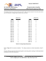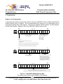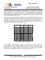
1
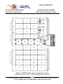
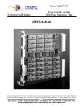
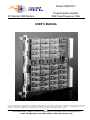
Model VM32PAFF Programmable Amplifier With Fixed Frequency Filter 32 Channel VME Module USER’S MANUAL We hope the information given here will be helpful. The information is based on data and our best knowledge, and we consider the information to be true and accurate. Please read all statements, recommendations or suggestions herein in conjunction with our conditions of sale which apply to all goods supplied by us. We assume no responsibility for the use of these statements, recommendations or suggestions, nor do we intend them as a recommendation for any use which would infringe any patent or copyright. 1 1784 Chessie Lane., Ottawa, IL 61350 • Tel: 800/252-7074, 815/434-7800 • FAX:815/434-8176 e-mail: [email protected] • Web Address: http://www.freqdev.com Model VM32PAFF 32 Channel VME Module Contents, Figures and Tables Programmable Amplifier With Fixed Frequency Filter Contents 1. Introduction .................................................................................................................................................3 Features/Benefits ................................................................................................................................3 2. Specifications..............................................................................................................................................4 3. Description..................................................................................................................................................5 VME Bus Interface and Input/Output Connections .............................................................................5 Programmable Gain Amplifiers ...........................................................................................................7 Anti-Alias Filters ..................................................................................................................................7 Output Amplifiers.................................................................................................................................7 4. Hardware Preparation.................................................................................................................................8 Unpacking and Inspection...................................................................................................................8 Hardware Configuration ......................................................................................................................9 Board Installation ..............................................................................................................................11 I/O Connections and the Front Panel................................................................................................11 Connector/Cable Information and I/O Connections ..........................................................................13 5. Programming ............................................................................................................................................15 Register Level Programming.............................................................................................................15 Programming Procedure ...................................................................................................................17 Programming Considerations............................................................................................................17 6. Troubleshooting and Technical Support ...................................................................................................19 7. Warranty Information ................................................................................................................................20 Limitation of Liability..........................................................................................................................20 8. Ordering Guide .........................................................................................................................................21 Figures Figure 3-1: VM32PAFF Simplified Functional Block Diagram. .......................................................................6 Figure 3-2 (a) and (b): A daughter module. ....................................................................................................7 Figure 4-1: VM32PAFF Base Address Configuration Jumpers. ...................................................................10 Figure 4-2: VM32PAFF Front Panel .............................................................................................................12 Figure 5-1: VM32PAFF VMEbus Memory Map. ...........................................................................................15 Tables Table 4-1: Analog Input Connections. ..........................................................................................................13 Table 4-2: Analog Output Connections.........................................................................................................14 Table 5-1: DATA register gain settings. ........................................................................................................16 2 1784 Chessie Lane., Ottawa, IL 61350 • Tel: 800/252-7074, 815/434-7800 • FAX:815/434-8176 e-mail: [email protected] • Web Address: http://www.freqdev.com Model VM32PAFF 32 Channel VME Module Introduction Programmable Amplifier With Fixed Frequency Filter 1. Introduction The VM32PAFF VMEbus family of amplifier/filter boards from Frequency Devices Inc. offer up to thirty-two channels of software programmable differential input amplifiers combined with precision 3-pole fixed frequency Butterworth or Bessel linear analog filters on each channel. The boards are available in a single width B-size (6U) VME form factor and fully conform to VME Revision C.1 as an A16/D16 Slave. VM32PAFF’s provide simultaneous access to DC-coupled wideband signals. The boards receive up to thirty-two differential signal inputs through two shielded front panel connectors and provide signal buffering, software programmable gain from -12dB to +60dB in 6dB steps, and fixed frequency 3-pole low pass filtering for each channel. The boards may be configured with Butterworth or Bessel filters with cutoff frequencies from 100 Hz to 100 kHz. Available options include AC coupled input and/or differential output. Features/Benefits • Simultaneous access over 32 channels offers a low cost, versatile and convenient way to provide amplification and filtering. • Interchannel crosstalk <-90 dB provides precision per-formance solutions to design engineers, system integrators and OEM’s. • 3-pole Butterworth or Bessel transfer functions with a broad range of corner frequencies are offered to meet a wide range of applications. • High channel count density without sacrificing performance maximizes chassis utilization. 3 1784 Chessie Lane., Ottawa, IL 61350 • Tel: 800/252-7074, 815/434-7800 • FAX:815/434-8176 e-mail: [email protected] • Web Address: http://www.freqdev.com Model VM32PAFF 32 Channel VME Module Specifications Programmable Amplifier With Fixed Frequency Filter 2. Specifications (@ 25oC and Rated Power Input) Analog Input 1. Input Impedance 2. Maximum Input 3. AC Couple (Optional) 1 MΩ//22 pF ±15V Fixed frequency @ 10Hz Analog Output 4. Impedance 5. Linear Operating Range 6. Channel to Channel Crosstalk 7. Maximum Current 8. Offset Voltage 9. Offset Temp. Coeff., RTI 1Ω typ., 10Ω max. ±5V pk, Output clamped to ±9 V <-100 dB @ 1.0 kHz, <-90 dB @ 20 kHz 5.0 mA 2mV RTI, NTE 40mV max. ±(5 +100/G) μV/°C max. Filter Characteristics 10. Anti-alias filtering 11. Cut-off Frequency fc (-3dB) 12. Amplitude Match* 13. Phase Match* 14. Noise Voltage, RTI 15. Distortion PGA5, G=1X @ 1VRMS Output, RL=2kΩ 3-pole low-pass Butterworth or Bessel fixed frequency Fixed frequency from 100 Hz to 100 kHz ±0.1dB @ DC, linear to ±0.25dB at fc 0.2° typ., 1.0° max @ fc 20nV/ Hz @ 1 kHz, G = 1000 -83 dB, 1 kHz single ended -86 dB, 1 kHz differential Gain 16. Gain Programmimg (G) 17. Gain Accuracy @ DC 0.25X to 1024X in factors of 2:1 (before filtering) 32 chls. programmed over VMEbus with read-back ±0.1 dB max. VMEbus 18. Interface 19. Registers A16/D16, D08(EO) Slave Three active R/W registers in 64 byte blocks Power Supply 20. From VME Backplane Environmental 21. Operating 22. Storage 23. Humidity Mechanical 24. Card Size 25. No. of Input Channels 26. No. of Output Channels 27. Differential Output 28. Mating Connectors 29. Weight +5V – 1.0A max. ±12 – 0.7A max. each 0oC to +70oC -25oC to +85oC 0-95% non-condensing VMEbus 6U single slot 9.17 x 6.3 inches, (233 x 160 mm) 32 Differential - DC coupled 32 Single Ended - DC coupled, Two groups of 16 (Optional) Input: Male high density 78-pin D-sub, Quantity 1 Output: Female high density 44-pin D-sub, Quantity 2 1 lbs., (454 grams kg.) * Any two channels set to same gain and loading 4 1784 Chessie Lane., Ottawa, IL 61350 • Tel: 800/252-7074, 815/434-7800 • FAX:815/434-8176 e-mail: [email protected] • Web Address: http://www.freqdev.com Model VM32PAFF 32 Channel VME Module Description Programmable Amplifier With Fixed Frequency Filter 3. Description The VM32PAFF is a single width B-size (6U) VME model that consists of a motherboard and up to 32 daughter modules. The motherboard contains the VMEbus interface and input and output connections. Each daughter module is made up of two boards: a high precision programmable gain amplifier board and a 3-pole filter/buffer amplifier combination board. VME Bus Interface and Input/Output Connections The VM32PAFF appears on the VMEbus as a Revision C.1 compliant A16/D16 slave. The VMEbus backplane offers a software programmable interface to set the gain of each daughter module. Through the interface, a user can also read back individual channel gain settings. This VM32PAFF read/write or bidirectional access to the individual amplifier modules is especially useful when building auto-ranging systems and/or fault tolerant systems. Additionally, it is good for diagnosing system failures, for debugging newly developed systems, and for constructing reliable test header files. The motherboard uses an indexed channel addressing scheme and transfers gain data to/from the selected channel over a simple serial channel. Figure 3-1 is a simplified block diagram of the VM32PAFF showing one amplifier/filter channel and all of the common functions. The serial channel incorporates some features that are especially important when providing precision, low noise signal conditioning. When the board is not being accessed (the normal case during a test) the serial channel is entirely static. When the board is accessed to set or read back a channel gain, only the channel being accessed is clocked, so the other channels on the board see no logic transitions that could inject noise or induce DC offsets. The serial channel is slow compared to VMEbus transfer rates. Rather than hold the VMEbus while gain data is serialized and transferred to the selected channel, the VM32PAFF board uses a BUSY flag interlock while data transfer to/from the selected channel is taking place. The motherboard provides simultaneous access to up to 32 Differential - DC-coupled wideband input signals. It offers up to 32 Single-Ended – DC coupled output channels in four groups of eight. Available options include AC-coupled input channels and/or Differential output channels 5 1784 Chessie Lane., Ottawa, IL 61350 • Tel: 800/252-7074, 815/434-7800 • FAX:815/434-8176 e-mail: [email protected] • Web Address: http://www.freqdev.com Model VM32PAFF 32 Channel VME Module Description Programmable Amplifier With Fixed Frequency Filter Figure 3-1: VM32PAFF Simplified Functional Block Diagram. One out of 32 posible channels is shown. Programmable Gain Amplifiers The programmable gain amplifiers (PGA) are located on daughter modules, see Figure 3-2. There is one PGA for each channel, up to a maximum of 32 channels per VM32PAFF. The input to the gain amplifier is a precision instrumentation amplifier that provides a high impedance differential input with high common mode rejection capability. The differential inputs for the channel are converted to a single ended signal before being applied to the gain amplifier where the signal is amplified or attenuated by the value programmed by the user. The gain can be selected to vary between x0.25 (-12.04dB) to x1024 (+60.21dB) in steps of x2 (6.02dB). When power is first applied to the board, the gain of each channel is arbitrary. The user must program the board in order to established a given gain value. 6 1784 Chessie Lane., Ottawa, IL 61350 • Tel: 800/252-7074, 815/434-7800 • FAX:815/434-8176 e-mail: [email protected] • Web Address: http://www.freqdev.com Model VM32PAFF 32 Channel VME Module Description Programmable Amplifier With Fixed Frequency Filter (a) VMEBus Interface Output Amplifier Ch x IN + Ch x OUT Differential Input PGA 3-pole Low Pass Filter (b) Figure 3-2 (a) and (b): A daughter module. X represents the channel number of 1 up to 32. Anti-Alias Filters Each channel provides a fixed frequency 3-pole Bessel or Butterworth linear analog low-pass filter. The corner frequency for each filter is user specified between 100 Hz and 100 kHz. There is no bypass mode for the anti-alias filter. Output Amplifiers The output of each filter module is applied to the output amplifier. This output stage converts the signal to a differential output with a low output impedance. The output is clamped to ±9V on each wire of the diferential pair. This results in a linear operation range of ±5V. 7 1784 Chessie Lane., Ottawa, IL 61350 • Tel: 800/252-7074, 815/434-7800 • FAX:815/434-8176 e-mail: [email protected] • Web Address: http://www.freqdev.com Model VM32PAFF 32 Channel VME Module Hardware Preparation Programmable Amplifier With Fixed Frequency Filter 4. Hardware Preparation Unpacking and Inspection Before unpacking the VM32PAFF shipping container, carefully inspect the exterior of the package for evidence of damage. After noting areas of possible shipping damage, open and unpack the shipping container, being careful to preserve the container and packing materials in case they are needed later. CAUTION: The VM32PAFF Board is sensitive to STATIC ELECTRICITY. Use proper GROUNDING TECHNIQUES when handling the board. Carefully remove the VM32PAFF board from its anti-static bag and visually inspect for evidence of damage. If the board appears to be damaged in any way, notify the shipping carrier immediately. 8 1784 Chessie Lane., Ottawa, IL 61350 • Tel: 800/252-7074, 815/434-7800 • FAX:815/434-8176 e-mail: [email protected] • Web Address: http://www.freqdev.com Model VM32PAFF 32 Channel VME Module Hardware Preparation Programmable Amplifier With Fixed Frequency Filter Hardware Configuration Once the VM32PAFF VMEbus board has been removed from its anti-static bag and carefully inspected for damage, you are ready to configure the board's base address for your particular system. Communication to all amplifier/filter modules is done through three registers whose Base Address can be set throughout all of A16 space. A VM32PAFF board occupies a 64-byte block in A16 address space and may be configured on any 64-byte boundary. The user will need to set a Base Address that is appropiate for the VME system in which the VM32PAFF will be installed. The Base Address is the only hardware configuration on the VM32PAFF board. The factory set Base Address is 2000(hex). Before attempting to use the board, the user should set/verify the base address using the address jumper JP1 on the board. CAUTION: The VM32PAFF Board is sensitive to STATIC ELECTRICITY. Use proper GROUNDING TECHNIQUES when handling the board. To reconfigure the VM32PAFF Base Address, lay the board flat as shown in Figure 4-1. The ten position jumper block shown in Figure 4-1 is used to set the board's base address in A16 address space. The ten jumper positions correspond to address lines A15 through A06. Jumper position 06 corresponds to address line A06, jumper position 07 corresponds to A07, etc. An installed jumper sets a logic '1' while a missing jumper sets a logic '0'. For example, to set the VM32PAFF Base Adresss to 800(hex), install a jumper on position 11 which corresponds to A11. After the board's base address has been configured, the VM32PAFF is ready for installation in a VME system. 9 1784 Chessie Lane., Ottawa, IL 61350 • Tel: 800/252-7074, 815/434-7800 • FAX:815/434-8176 e-mail: [email protected] • Web Address: http://www.freqdev.com Model VM32PAFF 32 Channel VME Module Hardware Preparation Programmable Amplifier With Fixed Frequency Filter Figure 4-1: VM32PAFF Base Address Configuration Jumpers. An installed jumper sets a logic '1' while a missing jumper sets a logic '0'. 10 1784 Chessie Lane., Ottawa, IL 61350 • Tel: 800/252-7074, 815/434-7800 • FAX:815/434-8176 e-mail: [email protected] • Web Address: http://www.freqdev.com Model VM32PAFF 32 Channel VME Module Hardware Preparation Programmable Amplifier With Fixed Frequency Filter Board Installation Frequency Devices' VM32PAFF conforms mechanically, in every respect, to the single width VME "B" size (6U) form factor. Installation of a VM32PAFF board into a standard VME mainframe can proceed exactly as for any other standard single width "B" size (6U) VME board. CAUTION: The VM32PAFF Board is sensitive to STATIC ELECTRICITY. Use proper GROUNDING TECHNIQUES when handling the board. The VM32PAFF board may be installed in any available mainframe slot except Slot 0 (VMEbus Master). The board does not use VMEbus interrupts or bus mastering capabilities, but passes all VMEbus daisy chained signals automatically. The major considerations in locating the VM32PAFF board in the mainframe are for EMI and I/O signal cabling. To minimize interference from other boards in the system, it is good practice to keep one or more empty slots between analog signal conditioning boards and high speed digital boards in the system. When cabling the system, it is desirable to keep the analog signal cabling as short as possible and physically located away from high speed digital cabling and high voltage switching lines. I/O Connections and the Front Panel The following information is provided to assist the user/integrator in installing and interconnecting a VM32PAFF board into a VME system. Figure 4-2 shows the layout of the VM32PAFF front panel. The following sections provide detailed information about connectors, pinouts, and cabling. There are no front panel indicators or controls on the VM32PAFF. 11 1784 Chessie Lane., Ottawa, IL 61350 • Tel: 800/252-7074, 815/434-7800 • FAX:815/434-8176 e-mail: [email protected] • Web Address: http://www.freqdev.com Model VM32PAFF 32 Channel VME Module Hardware Preparation Programmable Amplifier With Fixed Frequency Filter VM32PAFF Figure 4-2: VM32PAFF Front Panel The analog input connector is a female 78-pin D-shell connector. The analog output connectors are two male 44-pin D-shell connectors. 12 1784 Chessie Lane., Ottawa, IL 61350 • Tel: 800/252-7074, 815/434-7800 • FAX:815/434-8176 e-mail: [email protected] • Web Address: http://www.freqdev.com Model VM32PAFF 32 Channel VME Module Hardware Preparation Programmable Amplifier With Fixed Frequency Filter Connector/Cable Information and I/O Connections The Analog Input connector is a 78-pin female "D" shell connector located near the bottom of the front panel. Analog Input connections are as follows: Function Channel 00 Hi Channel 00 Lo Channel 01 Hi Channel 01 Lo Channel 02 Hi Channel 02 Lo Channel 03 Hi Channel 03 Lo Channel 04 Hi Channel 04 Lo Channel 05 Hi Channel 05 Lo Channel 06 Hi Channel 06 Lo Channel 07 Hi Channel 07 Lo Channel 08 Hi Channel 08 Lo Channel 09 Hi Channel 09 Lo Channel 10 Hi Channel 10 Lo Channel 11 Hi Channel 11 Lo Channel 12 Hi Channel 12 Lo Channel 13Hi Channel 13 Lo Channel 14 Hi Channel 14 Lo Channel 15 Hi Channel 15 Lo Input Connector (J3) 78 Pin Female D-shell 69 70 50 51 31 32 11 12 71 72 52 53 33 34 13 14 73 74 54 55 35 36 15 16 75 76 56 57 37 38 17 18 Function Channel 16 Hi Channel 16 Lo Channel 17 Hi Channel 17 Lo Channel 18 Hi Channel 18 Lo Channel 19 Hi Channel 19 Lo Channel 20 Hi Channel 20 Lo Channel 21 Hi Channel 21 Lo Channel 22 Hi Channel 22 Lo Channel 23 Hi Channel 23 Lo Channel 24 Hi Channel 24 Lo Channel 25 Hi Channel 25 Lo Channel 26 Hi Channel 26 Lo Channel 27 Hi Channel 27 Lo Channel 28 Hi Channel 28 Lo Channel 29Hi Channel 29 Lo Channel 30 Hi Channel 30 Lo Channel 31 Hi Channel 31 Lo Input Connector (J3) (Cont’d) 78 Pin Female D-shell 61 62 42 43 23 24 3 4 63 64 44 45 25 26 5 6 65 66 46 47 27 28 7 8 67 68 48 49 29 30 9 10 Table 4-1: Analog Input Connections. Refer to Figure 4-2 for connector orientation. The mating connector is a male high-density 78-pin D-sub . Frequency Devices recommends that input signals be wired using cable consisting of individually shielded twisted pairs of #22 AWG stranded wire. 13 1784 Chessie Lane., Ottawa, IL 61350 • Tel: 800/252-7074, 815/434-7800 • FAX:815/434-8176 e-mail: [email protected] • Web Address: http://www.freqdev.com Model VM32PAFF 32 Channel VME Module Hardware Preparation Programmable Amplifier With Fixed Frequency Filter The Analog Outputs are carried on two 44-pin male "D" shell connectors located in the center and near the top of the front panel. Analog Output connections are as follows: Function Channel 00 Hi Channel 00 Lo Channel 01 Hi Channel 01 Lo Channel 02 Hi Channel 02 Lo Channel 03 Hi Channel 03 Lo Channel 04 Hi Channel 04 Lo Channel 05 Hi Channel 05 Lo Channel 06 Hi Channel 06 Lo Channel 07 Hi Channel 07 Lo Channel 08 Hi Channel 08 Lo Channel 09 Hi Channel 09 Lo Channel 10 Hi Channel 10 Lo Channel 11 Hi Channel 11 Lo Channel 12 Hi Channel 12 Lo Channel 13Hi Channel 13 Lo Channel 14 Hi Channel 14 Lo Channel 15 Hi Channel 15 Lo Output Connector Channels 00-15 (J1) 44 Pin Male D-shell 33 32 19 18 4 3 35 34 21 20 6 5 37 36 23 22 8 7 39 38 25 24 10 9 41 40 27 26 12 11 43 42 Function Channel 16 Hi Channel 16 Lo Channel 17 Hi Channel 17 Lo Channel 18 Hi Channel 18 Lo Channel 19 Hi Channel 19 Lo Channel 20 Hi Channel 20 Lo Channel 21 Hi Channel 21 Lo Channel 22 Hi Channel 22 Lo Channel 23 Hi Channel 23 Lo Channel 24 Hi Channel 24 Lo Channel 25 Hi Channel 25 Lo Channel 26 Hi Channel 26 Lo Channel 27 Hi Channel 27 Lo Channel 28 Hi Channel 28 Lo Channel 29Hi Channel 29 Lo Channel 30 Hi Channel 30 Lo Channel 31 Hi Channel 31 Lo Output Connector Channels 16-31 (J2) 44 Pin Male D-shell 33 32 19 18 4 3 35 34 21 20 6 5 37 36 23 22 8 7 39 38 25 24 10 9 41 40 27 26 12 11 43 42 Table 4-2: Analog Output Connections. Refer to Figure 4-2 for connector orientation. The mating connectors are female high-density 44-pin Dsubs. Frequency Devices recommends that output signals be wired using cable consisting of individually shielded twisted pairs of #22 AWG stranded wire. 14 1784 Chessie Lane., Ottawa, IL 61350 • Tel: 800/252-7074, 815/434-7800 • FAX:815/434-8176 e-mail: [email protected] • Web Address: http://www.freqdev.com Model VM32PAFF 32 Channel VME Module Programming Programmable Amplifier With Fixed Frequency Filter 5. Programming Register Level Programming A register-based read/write programming interface makes the VM32PAFF family of VMEbus amplifier/filter boards extremely easy to program. All the programmable gain modules on the motherboard may be programmed through three 16-bit registers. These are the Channel Address Register, the Data Register, and the Reset Register. Figure 5-1 shows the VM32PAFF VMEbus memory map. (MSB) (LSB) B15 BUSY B08 B07 0 0 0 0 0 0 0 0 B00 0 0 ‘0’ indicates bit always reads zero Write data is ignored CH4 CH3 CH2 CH1 CH0 Binary address of channel selected for data read or write operation. 00000 = Channel 0 00001 = Channel 1 11110 = Channel 30 11111 = Channel 31 BUSY interlock: ‘1’ indicates on-board serial channel is busy formatting and transferring data. Automatically sets to ‘1’ upon writing gain data to DATA and upon writing to RESET. User writes ‘1’ to initiate readback og gain setting for channel pointed to by CH[4:0]. Automatically clears when transfer to/from the selected channel is complete. (MSB) (LSB) B15 0 B08 B07 0 0 0 0 0 0 0 0 B00 0 0 ‘0’ indicates bit always reads zero Write data is ignored 0 G3 G2 G1 G0 Binary representation of channel gain, in 6dB steps. Writing data to these bits when BUSY is clear sets the gain of the channel pointed to by CH[4:0],. When readback of a channel’s gain setting is requested by setting BUSY along with CH[4:0], the current channel gain setting appears here once BUSY clears. (MSB) (LSB) B15 X B08 B07 X X X X X X X X B00 X X X X X X X Any write to this location (word or byte) causes all channels to reset to the minimum gain, using the BUSY interlock. The data written is irrelevant. Reading this location will return random data. Immediately after a write to RESET completes (BUSY = 0), data read back in DATA, for any channel, will be 0x0000. Figure 5-1: VM32PAFF VMEbus Memory Map. The memory map consists of three VMEbus 16-bit registers. 15 1784 Chessie Lane., Ottawa, IL 61350 • Tel: 800/252-7074, 815/434-7800 • FAX:815/434-8176 e-mail: [email protected] • Web Address: http://www.freqdev.com Model VM32PAFF 32 Channel VME Module Programming Programmable Amplifier With Fixed Frequency Filter The Channel Address Register or CHADR (located at Base Address + 0) holds the address of the daughter module being addressed. The first amplifier channel, Channel 0, has an address of (00)x and the last amplifier channel, Channel 31, has an address of (1F)x. The channel addresses occupy the lowest five LSB’s of CHADR, that is, from B00 up to B04. One bit of this register is also used as a flag to indicate that the serial interface is busy and new data cannot be accepted until this bit is cleared. This BUSY interlock bit is located at the MSB of CHADR, or B15. The Data Register or DATA (located at Base Address + 2) holds the binary representation of a specific channel gain. Only the four lowest LSB’s of DATA are used. Writing data to these bits when BUSY is clear, sets the gain of the channel pointed to by CHADR. When a readback of a channel’s gain setting is requested by setting BUSY, the current channel gain setting appears in DATA once BUSY clears. The lowest gain setting (-12dB) is set by writing a (0)x to DATA and the highest gain setting (+60dB) is set by writing a (C)x to DATA. Table 5-1 shows DATA gain settings. Gain Weight Gain (Vo/Vi) ¼ ½ 1 2 4 8 16 32 64 128 256 512 1024 (dB) -12.04 -6.02 0.00 +6.02 +12.04 +18.06 +24.08 +30.10 +36.12 +42.14 +48.16 +54.19 +60.21 Encoded Value (decimal) 0 1 2 3 4 5 6 7 8 9 10 11 12 Encoded Value (hex) 0 1 2 3 4 5 6 7 8 9 A B C Table 5-1: DATA register gain settings. The Reset Register or RESET (located at Base Address + 4) allows the user to set all channels on the board simultaneously to their minimum gain setting. This is useful for system initialization and in autoranging applications. Writing anything to RESET transfers all zero data to all of the channels simultaneously. The data written is irrelevant. Readback requests on this location return random data. The reset function uses the BUSY interlock just as a normal write to DATA would. 16 1784 Chessie Lane., Ottawa, IL 61350 • Tel: 800/252-7074, 815/434-7800 • FAX:815/434-8176 e-mail: [email protected] • Web Address: http://www.freqdev.com Model VM32PAFF 32 Channel VME Module Programming Programmable Amplifier With Fixed Frequency Filter Programming Procedure To write gain data to a channel, the user first reads the CHADR (Base Address + 0) and tests its BUSY bit to see if the serial interface is busy. If BUSY is set, the user can go on to other things and come back to the board later, or the user can poll CHADR, waiting for BUSY to clear. Once BUSY is found clear the user writes the desired channel address to CHADR. The user must also make sure to write ‘0’ to the BUSY bit. Once the desired channel has been selected, the user then sets that channel’s gain by writing the desired gain data to DATA (Base Address + 2). The VM32PAFF automatically sets the BUSY bit in the CHADR register to indicate that the serial bus is transferring data. The BUSY bit is automatically cleared once the transfer is complete. The serial channel will be busy for approximately 4 microseconds. To read a channel's gain setting, the user first tests the BUSY bit to see if the serial interface is busy by reading CHADR’s BUSY bit. If BUSY is set, the user can go on to other things and come back to the board later, or the user can poll CHADR, waiting for BUSY to clear. Once BUSY is found clear, the user writes the desired channel address to CHADR, making sure to write a '1' to the BUSY bit. The serial interface accesses gain data from the selected channel and clears the BUSY bit in CHADR when the requested data is available in DATA. The requested data is available in DATA approximately 4 microseconds after writing to CHADR. Please note, when a flag can be controlled by two or more systems, instructions that generate read/modify/write cycles (or read followed by write cycles) should be avoided while testing the state of the BUSY bit. The safest way to test BUSY is to read CHADR into a local register and then test the state of the BUSY bit in the registered copy. In addition to VM32PAFF register map, Figure 5-1 also defines the read/write function of each bit. Notice that registers may be accessed as words or as bytes. Programming Considerations There are some considerations that the user must take into account for when trying to program the VM32PAFF. • Attempting to access the VM32PAFF board in other than A16 address space will cause a bus timeout. • Attempting long word access or unaligned transfers will cause the board to respond to the bus cycle with a bus error (BERR). • Changing the channel address while BUSY is set results in erroneous data during a data read operation and will corrupt the settings of two or more channels during a data write operation. • VM32PAFF hardware prevents changing of the channel selection while BUSY. • Writing to the Data Register or the Reset Register while BUSY is set is inhibited in hardware. None of these events are flagged by the board, so it is important to use the BUSY interlock before writing to any register. 17 1784 Chessie Lane., Ottawa, IL 61350 • Tel: 800/252-7074, 815/434-7800 • FAX:815/434-8176 e-mail: [email protected] • Web Address: http://www.freqdev.com Model VM32PAFF 32 Channel VME Module Programming • • • Programmable Amplifier With Fixed Frequency Filter Reading the Data Register while BUSY is set will yield erroneous data but will not impair board operation or contaminate any channel settings. This event is not flagged, so it is important to use the BUSY interlock before reading the Data Register. It is not possible to write '0' to the BUSY bit from the VMEbus, so this is not an error. Attempting to write '1' to the BUSY bit when it is already set is also not an error condition and therefore is not flagged. Attempting to set a channel's gain beyond the normal gain range will cause the channel to automatically set to its maximum gain. If the channel's gain setting is subsequently read back, the proper code for maximum gain will be returned. 18 1784 Chessie Lane., Ottawa, IL 61350 • Tel: 800/252-7074, 815/434-7800 • FAX:815/434-8176 e-mail: [email protected] • Web Address: http://www.freqdev.com Model VM32PAFF 32 Channel VME Module Troubleshooting and Technical Inrformation Programmable Amplifier With Fixed Frequency Filter 6. Troubleshooting and Technical Support If you have difficulty installing the VM32PAFF board, or if the board fails to operate properly, contact Frequency Devices for technical assistance. Technical assistance is available weekdays 8:00 AM to 4:30 PM Central time at 815-434-7800 or 800-252-7074. Inquiries may also be faxed to 815-434-8176 or emailed to [email protected]. If you need to contact Frequency Devices in writing, our address is: 1784 Chessie Lane Ottawa, IL 61350 Attn: Customer Service Please have the following information handy prior to contacting Frequency Devices for assistance: Model Number and Serial Number Purchase Order Number Your "Bill To" and "Ship To" addresses If Frequency Devices determines the board must be returned to the factory, you will be issued a Return Material Authorization (RMA) number. Use this number on all shipping containers, repair purchase orders, and shipping documents. DO NOT ATTEMPT TO RETURN BOARDS WITHOUT FIRST OBTAINING AN RMA NUMBER. CAUTION: The VM32PAFF Board is sensitive to STATIC ELECTRICITY. Use proper GROUNDING TECHNIQUES when handling the board. 19 1784 Chessie Lane., Ottawa, IL 61350 • Tel: 800/252-7074, 815/434-7800 • FAX:815/434-8176 e-mail: [email protected] • Web Address: http://www.freqdev.com Model VM32PAFF 32 Channel VME Module Warranty Information Programmable Amplifier With Fixed Frequency Filter 7. Warranty Information Unless otherwise specified in writing by FDI, all FDI products sold hereunder are warranted against defects in workmanship and material under normal use and service for a period of one (1) year from the date of shipment, except that, where applicable liability for defective components purchased by FDI and are resold to the purchaser hereunder shall conform and be limited to the obligations prescribed by the original manafacturer's warranties applicable to such components. All warranties hereunder are contingent upon proper use in the application for which the product was intended and do not cover products which have been modified or repaired without FDI approval or which have been subjected to neglect, accident, improper installation or application or on which the original identification marks have been removed or altered. These warranties will not apply if adjustment, repair or parts replacement is required because of accident, neglect, misuse, power failure, transportation or other causes other than ordinary use. FDI's responsibility under the above warranty shall be limited to the repair or replacement, at FDI's option, free of charge to the purchaser, of any component which fails during the one-year period; provided that the purchaser has promptly reported such failure to FDI in writing and FDI has, upon inspection, found such components to be defective. The purchaser must obtain shipping instructions for the return of any item under this warranty provision and compliance with such instructions shall be a condition of this waranty. EXCEPT FOR EXPRESS WARRANTIES STATED ABOVE, FDI DISCLAIMS ALL WARRANTIES WITH REGARD TO THE PRODUCTS SOLD HEREUNDER, INCLUDING ALL IMPLIED WARRANTIES OF MERCHANTABILITY AND FITNESS. Limitation of Liability Expressed warranties stated herein are in lieu of all obligations or liabilities on the part of FDI for damages, including but not limited to consequential damages arising out of or in connection with the use or performance of the product. 20 1784 Chessie Lane., Ottawa, IL 61350 • Tel: 800/252-7074, 815/434-7800 • FAX:815/434-8176 e-mail: [email protected] • Web Address: http://www.freqdev.com Model VM32PAFF 32 Channel VME Module Ordering Guide Programmable Amplifier With Fixed Frequency Filter 8. Ordering Guide VM32PAFF Ordering Guide For flexibility in many applications the Frequency Devices VM32PAFF VMEbus Board may be ordered with 8, 16, or 32 amplifier/filter modules. Figure 4-1 indicates the location of each channel. Transfer Function B - Butterworth L - Bessel | | | | | | Options A-AC Coupled Input D-Differential Output VM32PAFF-16-PGAB5-75kHz-D Channels 8, 16 or 32 | | | | -3dB Corner Frequency e.g. 100Hz, 75 kHz, 100 kHz We hope the information given here will be helpful. The information is based on data and our best knowledge, and we consider the information to be true and accurate. Please read all statements, recommendations or suggestions herein in conjunction with our conditions of sale which apply to all goods supplied by us. We assume no responsibility for the use of these statements, recommendations or suggestions, nor do we intend them as a recommendation for any use which would infringe any patent or copyright. 21 1784 Chessie Lane., Ottawa, IL 61350 • Tel: 800/252-7074, 815/434-7800 • FAX:815/434-8176 e-mail: [email protected] • Web Address: http://www.freqdev.com