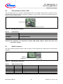
1
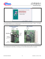
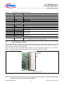
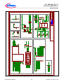
M otor Control Applic ation Kit For XMC1000 Family KIT_XM C1300_DC_V1 XMC1300 Drive Card V1.0 Board User„s M anual Revision 1.0, 2013-11-05 Mic rocontroll er Edition 2013-11-05 Published by Infineon Technologies AG 81726 Munich, Germany © 2013 Infineon Technologies AG All Rights Reserved. Legal Disclaimer The information given in this document shall in no event be regarded as a guarantee of conditions or characteristics. With respect to any examples or hints given herein, any typical values stated herein and/or any information regarding the application of the device, Infineon Technologies hereby disclaims any and all warranties and liabilities of any kind, including without limitation, warranties of non-infringement of intellectual property rights of any third party. Information For further information on technology, delivery terms and conditions and prices, please contact the nearest Infineon Technologies Office (www.infineon.com). Warnings Due to technical requirements, components may contain dangerous substances. For information on the types in question, please contact the nearest Infineon Technologies Office. Infineon Technologies components may be used in life-support devices or systems only with the express written approval of Infineon Technologies, if a failure of such components can reasonably be expected to cause the failure of that life-support device or system or to affect the safety or effectiveness of that device or system. Life support devices or systems are intended to be implanted in the human body or to support and/or maintain and sustain and/or protect human life. If they fail, it is reasonable to assume that the health of the user or other persons may be endangered. KIT_XMC1300_DC_V1 Drive Card XMC1300 V1 Revision History Page or Item Revision 1.0, 2013-11-05 Subjects (major changes since previous revision) Initial release Trademarks of Infineon Technologies AG AURIX™, C166™, CanPAK™, CIPOS™, CIPURSE™, EconoPACK™, CoolMOS™, CoolSET™, CORECONTROL™, CROSSAVE™, DAVE™, EasyPIM™, EconoBRIDGE™, EconoDUAL™, EconoPIM™, EiceDRIVER™, eupec™, FCOS™, HITFET™, HybridPACK™, I²RF™, ISOFACE™, IsoPACK™, MIPAQ™, ModSTACK™, my-d™, NovalithIC™, OptiMOS™, ORIGA™, PRIMARION™, PrimePACK™, PrimeSTACK™, PRO-SIL™, PROFET™, RASIC™, ReverSave™, SatRIC™, SIEGET™, SINDRION™, SIPMOS™, SmartLEWIS™, SOLID FLASH™, TEMPFET™, thinQ!™, TRENCHSTOP™, TriCore™. Other Trademarks Advance Design System™ (ADS) of Agilent Technologies, AMBA™, ARM™, MULTI-ICE™, KEIL™, PRIMECELL™, REALVIEW™, THUMB™, µVision™ of ARM Limited, UK. AUTOSAR™ is licensed by AUTOSAR development partnership. Bluetooth™ of Bluetooth SIG Inc. CAT-iq™ of DECT Forum. COLOSSUS™, FirstGPS™ of Trimble Navigation Ltd. EMV™ of EMVCo, LLC (Visa Holdings Inc.). EPCOS™ of Epcos AG. FLEXGO™ of Microsoft Corporation. FlexRay™ is licensed by FlexRay Consortium. HYPERTERMINAL™ of Hilgraeve Incorporated. IEC™ of Commission Electrotechnique Internationale. IrDA™ of Infrared Data Association Corporation. ISO™ of INTERNATIONAL ORGANIZATION FOR STANDARDIZATION. MATLAB™ of MathWorks, Inc. MAXIM™ of Maxim Integrated Products, Inc. MICROTEC™, NUCLEUS™ of Mentor Graphics Corporation. Mifare™ of NXP. MIPI™ of MIPI Alliance, Inc. MIPS™ of MIPS Technologies, Inc., USA. muRata™ of MURATA MANUFACTURING CO., MICROWAVE OFFICE™ (MWO) of Applied Wave Research Inc., OmniVision™ of OmniVision Technologies, Inc. Openwave™ Openwave Systems Inc. RED HAT™ Red Hat, Inc. RFMD™ RF Micro Devices, Inc. SIRIUS™ of Sirius Satellite Radio Inc. SOLARIS™ of Sun Microsystems, Inc. SPANSION™ of Spansion LLC Ltd. Symbian™ of Symbian Software Limited. TAIYO YUDEN™ of Taiyo Yuden Co. TEAKLITE™ of CEVA, Inc. TEKTRONIX™ of Tektronix Inc. TOKO™ of TOKO KABUSHIKI KAISHA TA. UNIX™ of X/Open Company Limited. VERILOG™, PALLADIUM™ of Cadence Design Systems, Inc. VLYNQ™ of Texas Instruments Incorporated. VXWORKS™, WIND RIVER™ of WIND RIVER SYSTEMS, INC. ZETEX™ of Diodes Zetex Limited. Last Trademarks Update 2011-02-24 Template: IFX_Template_2011-02-24.dot KIT_XMC1300_DC_V1 Drive Card XMC1300 V1 Table of Contents Table of Contents 1 1.1 1.2 Overview ............................................................................................................................................. 7 Key Features ........................................................................................................................................ 7 Block Diagram ...................................................................................................................................... 8 2 2.1 2.2 2.3 2.3.1 2.3.2 2.3.3 2.4 2.5 2.6 2.7 Hardware Description ........................................................................................................................ 9 Power Supply ....................................................................................................................................... 9 Clock Generation ............................................................................................................................... 11 Debug Interface .................................................................................................................................. 11 On-board USB Debugger ................................................................................................................... 11 Debug Connector (8-pin).................................................................................................................... 13 Infineon Debug Connector (16-pin) .................................................................................................... 13 Potentiometer and User LEDs ........................................................................................................... 15 USIC0 Connector ............................................................................................................................... 15 Hall Sensor and Encoder Connectors ................................................................................................ 16 Power Board Connector ..................................................................................................................... 17 3 3.1 3.2 3.3 Production Data................................................................................................................................ 19 Schematics ......................................................................................................................................... 19 Component Placement....................................................................................................................... 22 Bill of Material (BOM) ......................................................................................................................... 23 Board User's Manual 4 Revision 1.0, 2013-11-05 KIT_XMC1300_DC_V1 Drive Card XMC1300 V1 List of Figures List of Figures Figure 1 Figure 2 Figure 3 Figure 4 Figure 5 Figure 6 Figure 7 Figure 8 Figure 9 Figure 10 Figure 11 Figure 12 Figure 13 Figure 14 Figure 15 Figure 16 Figure 17 Block Diagram of KIT_XMC1300_DC_V1 ........................................................................................... 8 XMC1300 Drive Card (KIT_XMC1300_DC_V1) .................................................................................. 9 Power Supply Concept and Powering Options .................................................................................. 10 Block Diagram of Power Supply Concept .......................................................................................... 10 DAVE™ - “BMI Get Set” for XMC1000 Family................................................................................... 11 Installation of Serial Port Driver.......................................................................................................... 12 On-Board USB Debugger .................................................................................................................. 12 Pin Assignment of Debug Connector (8-pin) ..................................................................................... 13 Infineon Debug Connector (16-pin) .................................................................................................... 14 Potentiometer and LEDs .................................................................................................................... 15 USIC Interface Connector .................................................................................................................. 15 Hall Sensor and Encoder Connectors ................................................................................................ 16 Hall Sensor and Encoder Interface Circuitry ...................................................................................... 16 Power Board Connector ..................................................................................................................... 17 XMC1302 MCU, Power Supply, HALL and Encoder Interface, USIC0 interface .............................. 20 Isolated On-board Debugger.............................................................................................................. 21 Component Placement ....................................................................................................................... 22 Board User's Manual 5 Revision 1.0, 2013-11-05 KIT_XMC1300_DC_V1 Drive Card XMC1300 V1 List of Figures List of Tables Table 1 Table 2 Table 3 Table 4 Table 5 Table 6 Table 7 Power status LED‟s .............................................................................................................................. 9 Potentiometer ..................................................................................................................................... 15 USIC0 Connector X104...................................................................................................................... 15 HALL Sensor and Encoder Interfaces ............................................................................................... 17 Power Board Connector ..................................................................................................................... 18 Use Cases of PWM Signals ............................................................................................................... 19 BOM of KIT_XMC1300_DC_V1 Board .............................................................................................. 23 Board User's Manual 6 Revision 1.0, 2013-11-05 KIT_XMC1300_DC_V1 Drive Card XMC1300 V1 Overview Introduction This document describes the features and hardware details of the DriveCard XMC1300 V1 (KIT_XMC1300_DC_V1) designed to work with Infineon‟s inverter boards. This board is part of Infineon‟s Motor Control Application Kits. 1 Overview The drive card KIT_XMC1300_DC_V1 houses the XMC1302 Microcontroller from Infineon Technologies, a power board connector, a set of position interface circuits with hall and encoder connectors, a USIC interface and an isolated on-board debug interface. The board along with a three phase inverter demonstrates the capabilities of the XMC1302. The main use case for this board is to demonstrate the motor control features of the XMC1302 device including tool chain. The focus is safe operation under evaluation conditions. The board is neither cost nor size optimized and does not serve as a reference design. 1.1 Key Features The KIT_XMC1300_DC_V1 board is equipped with the following features Infineon XMC1302 (ARM® Cortex™-M0-based) Microcontroller, 200 kByte on-chip Flash, TSSOP38 Connection to power inverter via the power board connector Combined hall sensor and encoder interface USIC interface connector for connection of UART, SPI or I2C 6 LEDs − 2 Power indicating LEDs − 1 User LED (P0.4) − 1 Encoder enable LED − 2 Debug LEDs (DEBUG, COM) Potentiometer, connected to analog input P2.5 (ADC group 1, channel 7) Isolated Debug options − On-Board Debugger (SEGGER J-Link LITE) via USB connector − Infineon Debug connector 16-pin (0.1”) with DriveMonitor USB Stick V2 (KIT_DRIVEMONI_USB_V2) Isolated Connectivity − UART channel of On-Board Debugger (SEGGER J-Link LITE) via USB connector Power supply of MCU domain − Via power board connector (5V) Power supply of isolated debug domain − Via Debug USB connector − Via Infineon Debug connector 16-pin Board User's Manual 7 Revision 1.0, 2013-11-05 KIT_XMC1300_DC_V1 Drive Card XMC1300 V1 Overview 1.2 Block Diagram Figure 1 shows the functional block diagram of the KIT_XMC1300_DC_V1 board. For more information about the power supply domains please refer to chapter 2.1. The drive card has got the following building blocks: 1 Power Board Connector 1 set of position interface connectors (HALL, ENCODER) Encoder Enable signals via GPIOs (P0.10) 1 User LED connected to GPIOs (P0.4) Variable resistor (POTI) connected to GPIO P2.5 (ADC group 1, channel 7) USIC0 interface connector (P0.10, P0.14, P1.4, P1.5) Isolated On-board Debugger via Debug USB connector (Micro-USB) with UART channel (USIC0, channel 1) Optional Infineon Debug interface connector for Drive Monitor USB Stick V2 (KIT_DRIVEMONI_USB_V2) ENCODER IFX Debug isolation On-board Debugger XMC4200 Debug USB GPIO enable driver KIT_XMC1300_DC_V1 5V POTI POSIF0 USIC U0C0/C1 ADC XMC1300 TSSOP38 SWD/SPD USIC U0C1 11x CCU40 CCU80 Debug USIC0 Figure 1 XMC1300 Drive Card GPIO 1x PWM 6x PWM 1x IN 1x enable Power Board Connector HALL isolation BlockDiagram.emf Block Diagram of KIT_XMC1300_DC_V1 Board User's Manual 8 Revision 1.0, 2013-11-05 KIT_XMC1300_DC_V1 Drive Card XMC1300 V1 Hardware Description 2 Hardware Description The following sections give a detailed description of the hardware and how it can be used. Isolated Debug Domain Debug Connector Potentiometer User LED XMC1300 CPU Power GND Domain Power indicating LED Debug USB Connector Infineon Debug Connector On-board Debugger Encoder Enable LED Debug Encoder Connector Interface Power HALL Interface indicating LED Power Board Connector Board_Interfaces.emf Figure 2 2.1 XMC1300 Drive Card (KIT_XMC1300_DC_V1) Power Supply The KIT_XMC1300_DC_V1 board is designed with two galvanically isolated supply domains. On the left side, there is the debug domain, which contains a XMC4200 MCU as on-board debug controller (OBD) as well as level shifters to a 5V debug interface like the drive monitor USB stick (KIT_DRIVEMONI_USB_V2). The debug domain can be powered via the USB plug (5V) as well as the Infineon debug connector. On the middle to the right side there is the power GND supply domain, which provides the power supply for the MCU and the peripheral components. This supply domain is usually powered from the power board connector. The typical current drawn by the drive card at the power GND domain is about 25 mA. To indicate the power status of the KIT_XMC1300_DC_V1 board two power indicating LEDs are provided on board (see Figure 3). The LED will be “ON” when the corresponding power rail is powered. Table 1 Power status LED’s LED Reference LED101 LED201 Power Rail VDD5 VISO5 Voltage 5V 5V Note Power GND domain, must always be “ON” Debug supply domain, “ON” if debug domain is intened to be used. Figure 3 and Figure 4 show details of the power supply concept of the drive card. Board User's Manual 9 Revision 1.0, 2013-11-05 KIT_XMC1300_DC_V1 Drive Card XMC1300 V1 Hardware Description Isolated Debug Domain IFX1763: 3.3V Linear LDO Voltage Regulator Power GND Domain Debug Connector (5V – GND) Power indicating LED Debug USB Connector Infineon Debug Connector Power indicating LED Debug Connector (5V – GND) Power Board Connector Power.emf Power Supply Concept and Powering Options Power LED Drive Card XMC1300 V1 KIT_XMC1300_DC_V1 Debug USB Power LED VISO5 +5V VUSB5 VDD5 +5V VISO5 VDD5 IFX1763 isolation U202 VISO3.3 U201 XMC4200 OBD IFX Debug 16-pin Level Shifters 3.3V -> 5V IC101 UART SWD XMC1300 TSSOP38 Power Board Connector Figure 3 OBD_OFF# Power_Block.emf Figure 4 Block Diagram of Power Supply Concept Board User's Manual 10 Revision 1.0, 2013-11-05 KIT_XMC1300_DC_V1 Drive Card XMC1300 V1 Hardware Description 2.2 Clock Generation An internal oscillator provides the clock signal to the XMC1300 microcontroller. The CPU can be adjusted to maximum 32MHz (MCLK) whereas the PWM peripherals can be configured to use double of this clock (PCLK). 2.3 Debug Interface The KIT_XMC1300_DC_V1 is designed to use “Serial Wire Debug” (SWD) or “Single Pin Debug” (SPD) as debug interfaces. It supports debugging via different channels which are all galvanically isolated from the power GND supply domain: On-board Debugger Infineon Debug Connector (16-pin) with Debug and UART interface 2.3.1 On-board USB Debugger The on-board debugger [1] supports Serial Wire Debug (SWD) [2] o o SWIO SWCLK o o SWIO SWCLK P0.14 (SWD0) P0.15 (SWD0) or P1.3 (SWD1) P1.2 (SWD1) Single Pin Debug (SPD) [2] o SPD P0.14 (SPD0) or o SPD P1.3 (SPD1) Full Duplex UART communication via a Virtual COM port o o PC_RXD PC_TXD o o PC_RXD PC_TXD P1.2 USIC0CH1.DOUT0 P1.3 USIC0CH1.DX0A or P0.15 USIC0CH0.DOUT0 P0.14 USIC0CH0.DX0A [1] Attention: The firmware of the on-board debugger requires the latest J-Link driver (V4.62 or higher) and a Serial Port Driver (CDC driver) installed on your computer. Please check “Install J-Link Serial Port Driver” when installing the latest J-Link driver (see Figure 6) [2] The debug interface type (SPD or SWD) is selected via boot mode index (BMI) configuration. Changing the BMI is supported by the DAVE™ IDE and the “BMI Get Set” window (see Figure 5). Figure 5 DAVE™ - “BMI Get Set” for XMC1000 Family Board User's Manual 11 Revision 1.0, 2013-11-05 KIT_XMC1300_DC_V1 Drive Card XMC1300 V1 Hardware Description Figure 6 Installation of Serial Port Driver The on-board debugger can be accessed through the Debug USB connector shown in Figure 7. The Debug LED (LED202) shows the status during debugging. SEGGER J-LINK part (isolated) On-board Debugger XMC1300 part Debug Connector Debug LEDs Debug USB Connector isolation SWD & UART Infineon Debug Connector Debug Connector Debugger.emf Figure 7 On-Board USB Debugger When using an external debugger connected to the Infineon Debug Connector (16pin), the on-board debugger has to be switched off. This is done by connecting pin 6 of the Infineon Debug Connector to GNDISO. Board User's Manual 12 Revision 1.0, 2013-11-05 KIT_XMC1300_DC_V1 Drive Card XMC1300 V1 Hardware Description 2.3.2 Debug Connector (8-pin) The KIT_XMC1300_DC_V1 board supports debugging via SWD and SPD with the OBD as described in section 2.3.1. The pin assignment is provided in a way that both SWD ports (SWD0 and SWD1) can be selected. Please refer to Figure 8 for details on pin assignment. OBD Debug Connector (8-pin) Debug Connector (8-pin) SWCLK (SC) 1 2 SWIO (SD) P0.15 1 2 P0.14 +5V (VDD5) 3 4 GND +5V (VDD5) 3 4 GND GND 5 6 +5V (VDD5) GND 5 6 +5V (VDD5) PC_TX 7 8 PC_RX P1.3 7 8 P1.2 Debug_8pin.emf Figure 8 Pin Assignment of Debug Connector (8-pin) The default connection will provide the following set-up: Serial Wire Debug (SWD) o SWIO/SPD P0.14 (SWD0) o SWCLK P0.15 (SWD0) Full Duplex UART communication via a Virtual COM port o PC_RXD P1.2 USIC0CH1.DOUT0 o PC_TXD P1.3 USIC0CH1.DX0A While breaking off the J-LINK part of the PCB and connecting the debug interface with a ribbon cable, the direct connection will provide the same set-up. A reverse connection of the debug connector (pin1 to pin8) provides the other set-up: Serial Wire Debug (SWD) o SWIO/SPD P1.3 (SWD1) o SWCLK P1.2 (SWD1) Full Duplex UART communication via a Virtual COM port o o 2.3.3 PC_RXD PC_TXD P0.15 USIC0CH0.DOUT0 P0.14 USIC0CH0.DX0A Infineon Debug Connector (16-pin) The KIT_XMC1300_DC_V1 board supports debugging via Infineon‟s device access server (DAS), when using KIT_DRIVEMONI_USB_V2 as interface device. The latest release of DAS software can be downloaded from http://www.infineon.com/das. When using an external debugger, the on-board debugger (OBD) has to be switched off. This is done by connecting pin 6 to GNDISO. KIT_DRIVEMONI_USB_V2 already provides this connection and the OBD is disabled as soon as the connector is plugged in. Next to the SWD and SPD debug signals which are provided as unidirectional signals because of the galvanic isolation, UART signals can be accessed through this connector as well. Figure 9 shows the pin assignment of the connector, the following table lists the signals as well. Board User's Manual 13 Revision 1.0, 2013-11-05 KIT_XMC1300_DC_V1 Drive Card XMC1300 V1 Hardware Description Infineon Debug Connector (16-pin) SWD_DIR 1 2 +5V (VISO5) SWD_IN 3 4 GNDISO PC_RXD 5 6 OBD_OFF SWD_OUT 7 8 n.c. n.c. 9 10 n.c. SWCLK 11 12 n.c. n.c. 13 14 PC_TXD n.c. 15 16 n.c. Infineon_Debug_16pin.emf Figure 9 Pin No. 1 2 3 4 5 6 7 8 9 10 11 12 13 14 15 15 Infineon Debug Connector (16-pin) Signal Name SWD_DIR +5V (VISO5) SWD_IN GNDISO PC_RXD OBD_OFF# SWD_OUT n.c. n.c. n.c. SWCLK n.c. n.c. PC_TXD n.c. n.c. Board User's Manual I/O O I I I O O I - Serial Wire Debug Defines the direction of SWIO +5V supply of isolated debug domain Input signal of SWIO Ground of isolated debug domain UART Receive signal (P1.3, DOUT0 USIC0, channel1) Disable on-board debug device (Low active) Output signal of SWIO Not connected Not connected Not connected SWD clock signal Not connected Not connected UART Transmit signal (P1.2, DX0A, USIC0, channel1) Not connected Not connected 14 Revision 1.0, 2013-11-05 KIT_XMC1300_DC_V1 Drive Card XMC1300 V1 Hardware Description 2.4 Potentiometer and User LEDs The KIT_XMC1300_DC_V1 provides a potentiometer which is connected to ADC group1, channel7 and one user LED (P0.4). Next to the LED, a testpoint is available in order to easily connect an oscilloscope‟s probe for software controlled trigger signals. User LED Potentiometer Potentiometer_LED.emf Figure 10 Table 2 Potentiometer and LEDs Potentiometer Potentiometer R103 Connected to Port Pin P2.5 / G1_CH7 (Group 1, channel 7) User LEDs LED102 Connected to Port Pin P0.4 (LED) Attention: The testpoints are referenced to power GND supply domain. Hence they may carry hazzardous voltages. 2.5 USIC0 Connector The USIC Interface provides access to USIC 0 channel 0, which supports SPI, UART and I2C communication protocolls. USIC 0 channel 0 Figure 11 Table 3 Pin X104-1 X10⁴-2 X10⁴-3 X10⁴-4 X10⁴-5 X10⁴-6 USIC0.emf USIC Interface Connector USIC0 Connector X104 Port P1.4 VDD5 P1.5 P0.10 P0.14 GND Board User's Manual Peripherals USIC0_CH0.DX5E 5V USIC0_CH0.DOUT0 USIC0_CH0.SELO1 / DX2C USIC0_CH0.SCLKOUT GND 15 Comment Overlaps with ENENC Overlaps with SWD0/SPD0 Revision 1.0, 2013-11-05 KIT_XMC1300_DC_V1 Drive Card XMC1300 V1 Hardware Description 2.6 Hall Sensor and Encoder Connectors The KIT_XMC1300_DC_V1 provides two pairs of HALL and incremental encoder connectors as indicated in Figure 12. The encoder interface connector provides a differential input which is transformed into single ended signals by an interface IC. The HALL sensor interface provides a pull-up resistor for each HALL sensor signal as well as power supply for the HALL sensors 4 Encoder Enable LED Encoder Interface 6 5 Power Supply LED HALL Interface 7 LED at P0.4 POTI VDD5 LED-GE/D/0603 LED102 VDD5 VDD5 Port 1 - high current port LED101 LED-GN/D/0603 Hall_Encoder.emf IC101_P1 16 EI_POS2/P1.0 Figure 12 Hall Sensor and Encoder TP201Connectors 15 EB_POS1/P1.1 P1.0 P1.1 P1.2 P1.3 P1.4 P1.5 8 14 13 12 11 PC_RXD/P1.2 PC_TXD/P1.3 1 TP203 LED/P0.4 1 A R103 POTI A E 1k5R/0603 R104 1k5/0603 R105 no ass. no ass. Both P1.4 the HALL and the encoder signals are connected to the same POSIF interface. The ENENC-signal is used P1.5 to either enable the output signals of the encoder IC or to activate the powerS supply and pull-up resistor supply VDD5 10 POT VDD of the HALL sensor interface. As a result, both interfaces can be connectedVADC0.G1CH5 at the same time and the user can C101 TP202 220nby software which interface to 1use. Figure 13 shows the HALL sensor and encoder interface circuitry. select 9 VSS no ass.and peripheral GND GND Please refer to Table 4 for GND details on pin assignment. GND GND XMC1302-T038 HALL SENSOR CONNECTOR 330p/0603 f_cutoff = 14.6kHz GND VDD5 3 1k96/0402 5 4 3 2 1 R112 X101 1k96/0402 LED/P0.4 R109 C103 R111 n.m.(33k) V_W 1k96/0402 I_AVG R108 TP1 1 T102 BCR198W R110 V_DC I_PFC 1 T101 BCR198W 3 I_DC n.m./0603 R107 0R/0603 B 2 2 VDD5 ENENC/P0.10 R113 120R/0402 H0_POSIF.INA H0_POSIF.INB H0_POSIF.INI EA_POS0/P0.13 R114 120R/0402 EB_POS1/P1.1 R115 120R/0402 EI_POS2/P1.0 C MPT0,5/5-2,54 1 2 3 4 5 6 7 8 9 10 VDD5 GND ENENC/P0.10 U101 16 4 12 2 1 C107 15nF/0603 6 7 ENC0BGND PWM ENC0I+ R120 120R/0402 ENC0A+ ENC0B+ ENC0I+ ENCODER GND C106 15nF/0603 ENC0AENC0B+ R119 120R/0402 2 4 6 8 10 10 9 C108 15nF/0603 14 15 ENC0I- VCC GND 8 G G# GND 1A 1B 1Y 2A 2B 2Y 3A 3B 3Y 4A 4B 4Y 3 R118 JP101 1 3 5 7 9 LED103 1K5/0603 LED-GN/D/0603 ENC0A+ R116 120R/0402 ENC0AENC0BENC0I- 1k96/0402 V_DC V_U V_V V_W I_DC U_L U_H V_L V_H W_L W_H CTRAP/P0.12 ENPOW/P0.11 X102 C105 100nF/0402 VDD5 ENCODER LINE DRIVER AND CONNECTOR R117 VDD5 GND D 5 GND GND 11 EA_POS0/P0.13 AM26C32IPW 13 EB_POS1/P1.1 EI_POS2/P1.0 GND Figure 13 V1.1 / 28.10.2013 / AR Hall Legal Sensor and Encoder Interface Circuitry Disclaimer KIT_XMC1300_DC_V1 Revision The information given in this document shall in no event be regarded as a guarantee of conditions or characteristics. With respect to any examples or hints given herein, any typical values stated herein and/or any information regarding the application of the device, Infineon Technologies hereby disclaims any and all warranties and liabilities of any kind, including without limitation, warranties of non-infringement of intellectual property rights of any third party. Board User's Manual 4 5 16 6 E XMC1300 28/10/2013 09:34:45 7 Sheet: 2/3 8 1.0, 2013-11-05 KIT_XMC1300_DC_V1 Drive Card XMC1300 V1 Hardware Description Table 4 HALL Sensor and Encoder Interfaces Pin Port HALL Sensor Interface X101 1 GND 2 P1.0 3 P1.1 4 P0.13 5 VDD5 Encoder Interface X102 1 n.c. 2 VDD5 3 GND 4 n.c. 5 ENCA6 ENCA+ 7 ENCB8 ENCB+ 9 ENCI10 ENCI+ Enable Encoder LED103 P0.10 2.7 Peripheral POSIF0.IN2A POSIF0.IN1B POSIF0.IN0B HALL sensor power supply Encoder power supply POSIF0.IN0B POSIF0.IN1B POSIF0.IN2A High: Low: Enable Encoder Interface Enable HALL Interface including supply Power Board Connector The KIT_XMC1300_DC_V1 board provides a power board connector with all the signals required to control the power inverter. Next to the PWM output signals of CCU4 and CCU8 as well as the ADC signals, there are the power supply pins for the power GND domain. Figure 14 shows a picture of the power board connector. The pin and peripheral assignment can be found in Table 5. In addition, different use cases for three phase inverters can be found in Table 6. Power Board Connector PowerBoard_Con.emf Figure 14 Power Board Connector Attention: The power board connector is also providing the power supply for the power GND supply domain. Hence it may carry hazzardous voltages. Board User's Manual 17 Revision 1.0, 2013-11-05 KIT_XMC1300_DC_V1 Drive Card XMC1300 V1 Hardware Description Table 5 Power Board Connector X302 Female MAB32B2 FAB32Q2 A1 A16 A2 A15 A3 A14 A4 A13 A5 A12 A6 A11 A7 A10 A8 A9 A9 A8 A10 A7 A11 A6 A12 A5 A13 A4 A14 A3 A15 A2 A16 A1 B1 B16 B2 B15 B3 B14 B4 B13 B5 B12 B6 B11 B7 B10 B8 B9 B9 B8 B10 B7 B11 B6 B12 B5 B13 B4 B14 B3 B15 B2 B16 B1 Function on Power Inverter GND PFC Gate IPFC VPFC VBEMF_U / IU (2) VBEMF_V / IV (2) VBEMF_W / IW (2) I_AVG / IDClink (2) U1_L U1_H V1_L V1_H W1_L W1_H CTRAP1 ENPOW1 VCC 5V Brake Gate Brake temp VDClink VBEMF_U / IU (1) VBEMF_V / IV (1) VBEMF_W / IW (1) IDClink (1) U0_L U0_H V0_L V0_H W0_L W0_H CTRAP0 ENPOW0 Port Peripherals VSS, VSSP P0.5 P2.2 P2.4 P2.9 P2.10 P2.11 P2.1 VDD, VDDP P2.3 P2.6 P2.8 P2.0 P2.7 P0.1 P0.0 P0.6 P0.7 P0.9 & P0.3 P0.8 & P0.2 P0.12 P0.11 CCU40.CC40 VADC0.G0CH7 VADC0.G0CH2 VADC0.G0CH3 VADC0.G0CH4 VADC0.G0CH6 CMP2.OUT ACMP2.INN VADC0.G1CH6 VADC0.G1CH4 VADC0.G1CH2 VADC0.G1CH3 VADC0.G1CH5 VADC0.G0CH0 VADC0.G0CH1 VADC0.G0CH5 VADC0.G1CH0 VADC0.G1CH1 CCU80.OUT01 CCU80.OUT00 CCU80.OUT11 CCU80.OUT10 CCU80.OUT21 CCU80.OUT03 CCU80.OUT20 CCU80.OUT02 CCU80.IN0A,IN1A,IN2A,IN3A GPIO Note: Please note that the numbering of the power board connector at the drive card is inverse to the numbering at the power board. Board User's Manual 18 Revision 1.0, 2013-11-05 KIT_XMC1300_DC_V1 Drive Card XMC1300 V1 Production Data Table 6 Use Cases of PWM Signals X302 (MAB32B2) Function Port 2-Level Inverter with CCU80 B9 U0_L P0.1 B10 U0_H P0.0 B11 V0_L P0.6 B12 V0_H P0.7 B13 W0_L P0.9 B14 W0_H P0.8 B15 CTRAP0 P0.12 B16 ENPOW0 P0.11 2-Level Inverter with CCU80 (2 slices only) B9 U0_L P0.1 B10 U0_H P0.0 B11 V0_L P0.6 B12 V0_H P0.7 B13 W0_L P0.3 B14 W0_H P0.2 B15 CTRAP0 P0.12 B16 Enable0 P0.11 3 Production Data 3.1 Schematics Peripheral CCU80.OUT01 CCU80.OUT00 CCU80.OUT11 CCU80.OUT10 CCU80.OUT21 CCU80.OUT20 CCU80.IN0A,IN1A,IN2A,IN3A GPIO CCU80.OUT01 CCU80.OUT00 CCU80.OUT11 CCU80.OUT10 CCU80.OUT03 CCU80.OUT02 CCU80.IN0A,IN1A,IN2A,IN3A GPIO This chapter contains the schematics for the drive card: XMC1302 MCU, Power Supply, HALL and Encoder Interface, USIC0 interface Isolated On-board Debugger The board has been designed with Eagle. The full PCB design data of this board can also be downloaded from www.infineon.com/xmc-dev. Board User's Manual 19 Revision 1.0, 2013-11-05 E D C B A 1 P1.4 P1.5 SWIO/P0.14 SSC and ASC GND 1 2 3 4 5 6 7 8 n.m. 1 3 5 X10⁴ 2 4 6 25 100n XMC1302-T038 VSSP VDDP ORC 2 C104 S&H1 G1.CH1 G1.CH0 G1.CH4 G1.CH2 G1.CH3 G1.CH6 G1.CH7 CMP0 S&H1 G1.CH5 S&H0 G0.CH7 G0.CH6 G0.CH5 100nF/0402 ACMP CMP2 CMP1 3 MAB32B2 MAB32B2 X103-A1 X103-B1 X103-A2 X103-B2 X103-A3 X103-B3 X103-A4 X103-B4 X103-A5 X103-B5 X103-A6 X103-B6 X103-A7 X103-B7 X103-A8 X103-B8 X103-A9 X103-B9 X103-A10 X103-B10 X103-A11 X103-B11 X103-A12 X103-B12 X103-A13 X103-B13 X103-A14 X103-B14 X103-A15 X103-B15 X103-A16 X103-B16 S&H0 G0.CH1 G0.CH2 G0.CH3 G0.CH4 G0.CH0 XMC1302-T038 P2.4 P2.5 P2.6 P2.7 P2.8 P2.9 P2.10 P2.11 ENENC/P0.10 GND 26 C102 Port 2 - analogue features IC101_P2 GND VDD5 0R PFC_GATE/CMP2.OUT I_PFC V_PFC I_U I_V I_W I_AVG Power Board Connector V_PFC POT V_U I_DC V_V I_U I_V I_W LED/P0.4 PFC_GATE/CMP2.OUT V_L V_H W_H W_L ENENC/P0.10 ENPOW/P0.11 CTRAP/P0.12 EA_POS0/P0.13 SWIO/P0.14 R106 SWCLK/P0.15 R101 R102 P0.0 P0.1 P0.2 P0.3 P0.4 P0.5 P0.6 P0.7 P0.8 P0.9 P0.10 P0.11 P0.12 P0.13 P0.14 P0.15 Port 0 - standard port 38 37 36 35 BLM18PG600 L101 ORC P2.3 P2.2 P2.1 P2.0 IC101_P1 V_DC V_U V_V V_W I_DC U_L U_H V_L V_H W_L W_H CTRAP/P0.12 ENPOW/P0.11 V_W V_DC I_PFC 9 10 16 15 14 13 12 11 GND 220n C101 GND PWM 4 LED/P0.4 330p/0603 f_cutoff = 14.6kHz R109 C103 JP101 1 2 3 4 5 6 7 8 9 10 R108 n.m.(33k) GND TP1 I_AVG VDD5 EI_POS2/P1.0 EB_POS1/P1.1 PC_RXD/P1.2 PC_TXD/P1.3 P1.4 P1.5 I_DC n.m./0603 R107 0R/0603 XMC1302-T038 VSS VDD P1.0 P1.1 P1.2 P1.3 P1.4 P1.5 Port 1 - high current port VDD5 GND no ass. 1 TP202 no ass. 1 TP201 T102 BCR198W GND 1 1 C108 15nF/0603 C107 15nF/0603 C106 15nF/0603 GND 14 15 10 9 6 7 2 1 4 12 16 GND 5 6 1 7 4Y 3Y 2Y 1Y GND no ass. AM26C32IPW 4A 4B 3A 3B 2A 2B 1A 1B G G# VCC U101 The information given in this document shall in no event be regarded as a guarantee of conditions or characteristics. With respect to any examples or hints given herein, any typical values stated herein and/or any information regarding the application of the device, Infineon Technologies hereby disclaims any and all warranties and liabilities of any kind, including without limitation, warranties of non-infringement of intellectual property rights of any third party. Legal Disclaimer ENC0I- ENC0I+ R120 120R/0402 ENC0B- ENC0B+ R119 120R/0402 ENC0A- ENC0A+ R116 120R/0402 7 TP203 H0_POSIF.INA H0_POSIF.INB H0_POSIF.INI GND ENCODER LINE DRIVER AND CONNECTOR MPT0,5/5-2,54 5 4 3 2 1 X101 T101 BCR198W LED/P0.4 LED at P0.4 HALL SENSOR CONNECTOR GND R105 IC101_P0 LED101 LED-GN/D/0603 1k5/0603 6 VDD5 17 18 4k7 19 4k7 20 21 22 23 24 27 28 29 30 31 32 33 34 P0.15 VDD5 Power Supply LED 2 3 U_H U_L 5 R110 R104 4 VDD5 3 R111 1k5R/0603 2 1k96/0402 LED-GE/D/0603 LED102 1k96/0402 2 3 R112 1 VDD5 VDD5 VDD5 1k96/0402 POTI 13 11 5 3 8 GND GND ENC0AENC0BENC0I- GND Sheet: 2/3 8 28/10/2013 09:34:45 KIT_XMC1300_DC_V1 XMC1300 V1.1 / 28.10.2013 / AR EI_POS2/P1.0 EB_POS1/P1.1 EA_POS0/P0.13 GND ENENC/P0.10 ENC0A+ ENC0B+ ENC0I+ EI_POS2/P1.0 EB_POS1/P1.1 EA_POS0/P0.13 ENENC/P0.10 2 4 6 8 10 ENCODER 1 3 5 7 9 X10² R115 120R/0402 R114 120R/0402 R113 120R/0402 8 S POT VADC0.G1CH5 GND VDD5 R103 POTI R117 C105 100nF/0402 E A 1k96/0402 20 R118 Board User's Manual LED103 1K5/0603 LED-GN/D/0603 Figure 15 VDD5 XMC1300 CORTEX-M0 Microcontroller in TSSOP38 Package E D C B A KIT_XMC1300_DC_V1 Drive Card XMC1300 V1 Production Data XMC1302 MCU, Power Supply, HALL and Encoder Interface, USIC0 interface Revision 1.0, 2013-11-05 E D C B DEBUG_LED# COM_LED# RXD TXD VISO3.3 Q201 12MHZ/S/3.2X2.5 1 GNDISO T202 BCR148W VISO3.3 T201 BSS223PW VISO3.3 VISO3.3 27 EPAD 32 34 33 29 30 8 9 18 17 24 25 26 no ass. GNDISO GNDISO 1 2 3 4 5 VISO3.3 X205 OBD_OFF# OBD_TCK OBD_TMS 510R/0603 GNDISO 100nF/0402 C201 21 RX SWD_IN 2 VCCB VCCA B1 A1 B2 ---> A2 GND DIR VCCB VCCA B1 A1 B2 ---> A2 GND DIR U206 VCCB VCCA B1 A1 B2 <--A2 GND DIR U207 3 GNDISO SN74LVC2T45DCT 8 7 6 4 GNDISO SN74LVC2T45DCT 8 SWCLK_ISO 7 6 TX 4 GNDISO GNDISO 100nF/0402 C218 8 7 6 4 Supply GNDISO SN74LVC2T45DCT SWD_DIR SWD_OUT U205 Analog Digital 1 2 3 5 1 2 3 5 1 2 3 5 USB_D- HIB_IO_0 VBAT P14.9 P14.8 P14.7 P14.6 P14.5 P14.4 P14.3 P14.0 P1.5 P1.4 P1.3 P1.2 P1.1 P1.0 P0.8 P0.7 P0.6 P0.5 P0.4 P0.3 P0.2 P0.1 P0.0 PC_RXD5 SWD_IN5 VISO5 GNDISO SWCLK5 PC_TXD5 VISO5 GNDISO SWD_DIR5 SWD_OUT5 VISO5 VDDC1 VDDC VDDP2 VDDP1 VDDP USB USB_D+ Hibernate/RTC XMC4200_QFN48 VSS EPAD PORST# TCK TMS XTAL1 XTAL2 RTC_XTAL_1 RTC_XTAL_2 VAREF VAGND P2.5 P2.4 P2.3 P2.2 P2.1 P2.0 The board includes an On-Board-Debugger (OBD) using a XMC microcontroller plus the J-link SW from Segger. The OBD may be designed as break-out or non break-out option. In both cases, the license usage of this OBD with the J-Link SW is limited to the delivered board. Segger J-Link OBD R205 CONTROL GPIOs RESET# GPIO-P0.3 DEBUG_LED# GPIO-P0.2 AUX_LED# GPIO-P0.1 OBD Voltage Level Shifter OBD_OFF# P14.9 UART2 (DM2) U1C0 RXD DX0A-P0.4 TXD DOUT0-P0.5 TX_ENABLE GPIO-P0.7 TXACTIVE# GPIO-P0.6 ADC AIN GNDISO GNDISO C206 15pF/0402 22 SWCLK_ISO 23 CS 31 6 41 28 5 3 4 7 10 19 20 11 12 13 14 15 16 35 36 37 38 39 40 42 43 44 45 46 47 48 1 2 TX RX R204 R206 4 GNDISO Isolation 33R/0402 33R/0402 GNDISO SWCLK_ISO CS SWD_OUT SWD_IN SWD_DIR DEBUG_LED# COM_LED# COM LED Level Shifter No RESET Pin UART SPD SWV JTAG C210 100nF/0402 SPI Slave U0C1 CS_IN DX2A-P2.3 CLK_IN DX1A-P2.4 PULL Select GPIO-P0.8 C211 100nF/0402 A C212 4.7uF/X7R/0805 U201 C213 100nF/0402 U0C0 GPIO-P1.3 DX0B-P1.4 DOUT0-P1.5 SCLKOUT-P1.1 SELO0-P1.0 R210 4 GNDISO C214 100nF/0402 3 C215 100nF/0402 SPI Master SWD DIR MISO MOSI CLK_OUT CS_OUT R213 GNDISO VISO3.3 VISO3.3 SWIO/P0.14/2.1E PC_RXD/P1.2/2.5A VISO5 8 6 4 2 1 X203 7 5 3 1 debug GND GND2 B1 B2 B3 B4 B5 B6 VDD2 Si8462BB-B-IS1 GND1 A1 A2 A3 A4 A5 A6 VDD1 U204 SWCLK/P0.15/2.1B 3 6 7 5 8 5 6 OUT BYP EXP SENSE/ADJ SWCLK5 SWD_DIR5 SWD_IN5 PC_RXD5 SWD_OUT5 VDD5 9 15 14 13 12 11 10 16 GND VDD5 GND OE A C202 10nF/0402 VCC GND Y U203 SWIO/P0.14/2.1E 5 3 4 GNDISO 4 9 2 1 TMS VDDP TDO GND1 NC1 GND2 TDI RESET TRST BRKOUT TCLK GND3 BRKIN NC3 NC2 NC4 PC_RXD/P1.2/2.5A 7 8 8 6 4 2 GND debug V1.1 / 28.10.2013 / AR SWCLK/P0.15/2.1B Sheet: 3/3 8 28/10/2013 09:34:45 KIT_XMC1300_DC_V1 OBD X204 PC_TXD/P1.3 PC_RXD/P1.2 SWIO/P0.14 GND R212 n.m./0402 R211 4k7/0402 PC_TXD/P1.3/2.5A 0R/0402 SWCLK/P0.15 GNDISO R215 VISO5 PC_TXD5 GNDISO VISO3.3 7 5 3 1 C OBD_OFF# A BAS3010A-03W X201 V201 DriveMonitor2 74LVC1G126GW 2 1 IFX1763_PADNOP GND GND GND EN IN U202 C209 1uF/0402 GNDISO PC_TXD/P1.3/2.5A GNDISO 8 SWCLK5 2 SWD_DIR5 3 SWD_OUT5 4 PC_TXD5 5 PC_RXD5 6 SWD_IN5 7 VISO5 OBD Isolation VUSB5 OBD 3.3V Power Supply GNDISO 7 Debug and UART Interface The information given in this document shall in no event be regarded as a guarantee of conditions or characteristics. With respect to any examples or hints given herein, any typical values stated herein and/or any information regarding the application of the device, Infineon Technologies hereby disclaims any and all warranties and liabilities of any kind, including without limitation, warranties of non-infringement of intellectual property rights of any third party. Legal Disclaimer GND VDD5 OBD Debug Connector GNDISOGNDISO 1 2 3 4 5 X202C L201 BLM18PG600 1k5/0603 LED201 LED-GN/D/0603 OBD Power Supply LED 6 R203 5 3 D1 C A R201 VUSB5 V203 ESD8V0L2B-03L 1 VISO3.3 C216 10uF/10V/0805 R202 R209 VISO5 V202 R207 R208 LED202 680R/0603 LED-GN/D/0603 2 D2 BAS3010A-03W 4k7/0402 10k/0402 LED203 680R/0603 LED-RT/D/0603 1M/0402 SWD_DIR SWD_IN SWD_OUT SWCLK C207 15pF/0402 10k/0402 10k/0402 ZX62-AB-5PA C208 100nF/0402 C203 10uF/10V/0805 On-board Debugger (OBD) and UART IF R214 1uF/0402 C204 10uF/10V/0805 2 1k/0402 21 C217 VDD5 Board User's Manual C205 100nF/0402 Figure 16 VDD5 1 E D C B A KIT_XMC1300_DC_V1 Drive Card XMC1300 V1 Production Data Isolated On-board Debugger Revision 1.0, 2013-11-05 1 2 3 KIT_XMC1300_DC_V1 Drive Card XMC1300 V1 Production Data C211 U204 C215 R205 C103 JP101 U_L POTI P2.5 G1CH7R117 R104 LED102 U101 R118 LED103 ENENC U_H V_L C108 R120 C107 R119 C106 R116 1 V_H X102 X102 W_L U203 X201 X203 SD 0 + Rx SC + 0 Tx +5V HA0 HA1 T101 GND R211 R112 R113 ADJ_301 HA2 C209 X203 GND R212 V201 Figure 17 ENABLE T102 1 2 3 4 5 R111 R114 R110 R115 X101 X101 HALL R105 T202 R214 1 W_H CTRAP U205 1 R108 R107 TP203 R210 U207 R109 DIN 41612-B/2 C102 LED P0.4 TP1 TP1 R213 C218 T201 C206 U206 XMC1300 LED101 X205 Q201 P1.4 C105 C217 C201 U201 C214 5V 1 L101 IC101 R103 R215 C207 P0.10 R106 R206 R204 LED203 LED202 R202 C210 C216 DEBUG C212 R201 COM C205 C202 X103 C104 b A1 a B1 C101 P0. 14 P1.5 GND C213 V203 X104 USIC0 X104 R101 C203 R207 R208 L201 U202 C204 C208 V202 X202 X204 debug X204 ADJ_303 P0.14 GND 5V P1.2 P0.15 5V GND P1.3 R203 Drive Card XMC1300 R102 Debug & COM (isolated) LED201 R209 Component Placement X202 3.2 GND 16 X103 ADJ_302 TP201 TP202 GND +5V Component Placement 1 2 Board User's Manual 22 3 Revision 1.0, 2013-11-05 KIT_XMC1300_DC_V1 Drive Card XMC1300 V1 Production Data 3.3 Bill of Material (BOM) Table 7 BOM of KIT_XMC1300_DC_V1 Board Pos. Qty No. Value Device Reference Des. R101, R102 R103 R104 R105, R203 R106 R107 R108 R109 R110, R111, R112, R117 R113, R114, R115, R116, R119, R120 R118 R201, R202 R204, R206 R205 R207, R211 R208, R210, R213 R209 R212 R214 R215 C101 C102 C103 C104, C105, C201, C205, C208, C210, C211, C213, C214, C215, C218 C106, C107, C108 C202 C203, C204, C216 C206, C207 C209, C217 C212 1 2 3 4 5 6 7 8 9 10 11 12 13 14 15 16 17 18 19 20 21 22 23 24 2 1 1 2 1 1 1 1 4 6 1 2 2 1 2 3 1 1 1 1 1 1 1 11 4k7 10k 1k5R/0603 1k5/0603 0R n.m./0603 0R/0603 n.m.(33k) 1k96/0402 120R/0402 1K5/0603 680R/0603 33R/0402 510R/0603 4k7/0402 10k/0402 1M/0402 n.m./0402 1k/0402 0R/0402 220n 100n 330p/0603 100nF/0402 RESISTOR 0603 25 26 27 28 29 30 31 32 33 34 35 36 37 38 39 40 41 42 3 1 3 2 2 1 2 2 4 1 1 2 1 1 1 1 1 1 15nF/0603 10nF/0402 10uF/10V/0805 15pF/0402 1uF/0402 4.7uF/X7R/0805 12MHZ/S/3.2X2.5 BLM18PG600 LED-GN/D/0603 LED-GE/D/0603 LED-RT/D/0603 BCR198W BSS223PW BCR148W XMC1302_TSSOP38 IFX1763 AM26C32IPW XMC4200_QFN48 CAPACITOR 0603 CAPACITOR 0402 CAPACITOR 0805K CAPACITOR 0402 CAPACITOR 0402 CAPACITOR 0805K CRYSTAL FERRIT BEAD LEDCHIPLED 0603 LEDCHIPLED 0603 LEDCHIPLED 0603 TRANSISTOR TRANSISTOR TRANSISTOR INFINEON MCU INFINEON LDO ENCODER IC INFINEON MCU Board User's Manual potentiometer RESISTOR 0603 RESISTOR 0603 RESISTOR 0603 RESISTOR 0603 RESISTOR 0603 RESISTOR 0603 RESISTOR 0402 RESISTOR 0402 RESISTOR 0603 RESISTOR 0603 RESISTOR 0402 RESISTOR 0603 RESISTOR 0402 RESISTOR 0402 RESISTOR 0603 RESISTOR 0402 RESISTOR 0402 RESISTOR 0402 CAPACITOR 0603 CAPACITOR 0603 CAPACITOR 0603 CAPACITOR 0402 23 Q201 L101, L201 LED101, LED103, LED201, LED202 LED102 LED203 T101, T102 T201 T202 IC101 U202 U101 U201 Revision 1.0, 2013-11-05 KIT_XMC1300_DC_V1 Drive Card XMC1300 V1 Production Data 43 44 45 46 47 48 49 50 51 52 53 54 1 1 3 2 1 1 1 1 1 1 2 1 Si8462BB-B-IS1 74LVC1G126GW SN74LVC2T45DCT BAS3010A-03W ESD8V0L2B-03L ZX62-AB-5PA W1*10 CONP_2X05 MAB32B2 MPT0,5/5-2,54 W2*4 W2*3 Board User's Manual ISOLATED DIGITAL LOGIC LOGIC BAT60 ESD DIODE MICRO-USB CONNECTOR CONNECTOR CONNECTOR CONNECTOR CONNECTOR (DEBUG) CONNECTOR (USIC) 24 U204 U203 U205, U206, U207 V201, V202 V203 X202 JP101 X102 X103 X101 X203, X204 X104 Revision 1.0, 2013-11-05 w w w . i n f i n e o n . c o m Published by Infineon Technologies AG