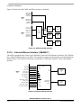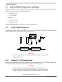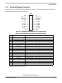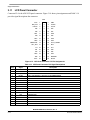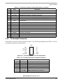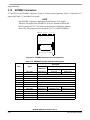
1
Freescale Semiconductor
User’s Manual
UMS-20956
Rev A, 08/2006
i.MX27 Application
Development System
User’s Manual
© Freescale Semiconductor, Inc., 2006. All rights reserved.
How to Reach Us:
Home Page:
www.freescale.com
E-mail:
[email protected]
USA/Europe or Locations Not Listed:
Freescale Semiconductor
Technical Information Center, CH370
1300 N. Alma School Road
Chandler, Arizona 85224
+1-800-521-6274 or +1-480-768-2130
[email protected]
Europe, Middle East, and Africa:
Freescale Halbleiter Deutschland GmbH
Technical Information Center
Schatzbogen 7
81829 Muenchen, Germany
+44 1296 380 456 (English)
+46 8 52200080 (English)
+49 89 92103 559 (German)
+33 1 69 35 48 48 (French)
[email protected]
Japan:
Freescale Semiconductor Japan Ltd.
Headquarters
ARCO Tower 15F
1-8-1, Shimo-Meguro, Meguro-ku,
Tokyo 153-0064
Japan
0120 191014 or +81 3 5437 9125
[email protected]
Asia/Pacific:
Freescale Semiconductor Hong Kong Ltd.
Technical Information Center
2 Dai King Street
Tai Po Industrial Estate
Tai Po, N.T., Hong Kong
+800 2666 8080
[email protected]
For Literature Requests Only:
Freescale Semiconductor Literature Distribution Center
P.O. Box 5405
Denver, Colorado 80217
1-800-441-2447 or 303-675-2140
Fax: 303-675-2150
[email protected]
UMS-20956
Rev A, 08/2006
RoHS-compliant and/or Pb-free versions of Freescale products have the functionality
and electrical characteristics of their non-RoHS-compliant and/or non-Pb-free
counterparts. For further information, see http://www.freescale.com or contact your
Freescale sales representative.
For information on Freescale’s Environmental Products program, go to
http://www.freescale.com/epp.
Information in this document is provided solely to enable system and software
implementers to use Freescale Semiconductor products. There are no express or
implied copyright licenses granted hereunder to design or fabricate any integrated
circuits or integrated circuits based on the information in this document.
Freescale Semiconductor reserves the right to make changes without further notice to
any products herein. Freescale Semiconductor makes no warranty, representation or
guarantee regarding the suitability of its products for any particular purpose, nor does
Freescale Semiconductor assume any liability arising out of the application or use of any
product or circuit, and specifically disclaims any and all liability, including without
limitation consequential or incidental damages. “Typical” parameters that may be
provided in Freescale Semiconductor data sheets and/or specifications can and do vary
in different applications and actual performance may vary over time. All operating
parameters, including “Typicals”, must be validated for each customer application by
customer’s technical experts. Freescale Semiconductor does not convey any license
under its patent rights nor the rights of others. Freescale Semiconductor products are
not designed, intended, or authorized for use as components in systems intended for
surgical implant into the body, or other applications intended to support or sustain life,
or for any other application in which the failure of the Freescale Semiconductor product
could create a situation where personal injury or death may occur. Should Buyer
purchase or use Freescale Semiconductor products for any such unintended or
unauthorized application, Buyer shall indemnify and hold Freescale Semiconductor and
its officers, employees, subsidiaries, affiliates, and distributors harmless against all
claims, costs, damages, and expenses, and reasonable attorney fees arising out of,
directly or indirectly, any claim of personal injury or death associated with such
unintended or unauthorized use, even if such claim alleges that Freescale
Semiconductor was negligent regarding the design or manufacture of the part.
Freescale™ and the Freescale logo are trademarks of Freescale Semiconductor, Inc.
All other product or service names are the property of their respective owners.
© Freescale Semiconductor, Inc. 2006. All rights reserved.
Chapter 1 General Information
1.1
1.2
1.3
1.4
1.5
Description . . . . . . . . . . . . . . . . . . . . . . . . . . . . . . . . . . . . . . . . . . . . . . . . . . . . . . . . . . . . . . . . .
MCIMX27ADSE Features . . . . . . . . . . . . . . . . . . . . . . . . . . . . . . . . . . . . . . . . . . . . . . . . . . . . .
System and User Requirements . . . . . . . . . . . . . . . . . . . . . . . . . . . . . . . . . . . . . . . . . . . . . . . . .
MCIMX27ADSE Diagram . . . . . . . . . . . . . . . . . . . . . . . . . . . . . . . . . . . . . . . . . . . . . . . . . . . . .
ADS Specifications. . . . . . . . . . . . . . . . . . . . . . . . . . . . . . . . . . . . . . . . . . . . . . . . . . . . . . . . . . .
1-1
1-1
1-2
1-3
1-6
Chapter 2 Configuration and Operation
2.1
2.2
2.2.1
2.2.2
2.2.3
2.2.4
2.2.5
2.2.6
2.2.7
2.2.8
2.2.9
2.3
2.3.1
2.3.2
2.3.3
2.3.4
2.3.5
2.3.6
2.3.7
2.3.8
2.3.9
2.3.10
2.3.11
2.3.12
2.3.13
2.3.14
2.3.15
2.4
2.4.1
2.4.2
2.4.3
2.4.4
2.4.5
2.4.6
2.4.7
2.4.8
Introduction. . . . . . . . . . . . . . . . . . . . . . . . . . . . . . . . . . . . . . . . . . . . . . . . . . . . . . . . . . . . . . . . . 2-1
Configuring Board Components . . . . . . . . . . . . . . . . . . . . . . . . . . . . . . . . . . . . . . . . . . . . . . . . . 2-1
DIP Switch S7 - Li-Cell select switch . . . . . . . . . . . . . . . . . . . . . . . . . . . . . . . . . . . . . . . . . 2-1
DIP Switch S18 - Boot Mode Switches . . . . . . . . . . . . . . . . . . . . . . . . . . . . . . . . . . . . . . . . 2-1
DIP Switch S9 - MC13783 USB Mode Switches. . . . . . . . . . . . . . . . . . . . . . . . . . . . . . . . . 2-2
DIP Switch S3 - MC13783 Audio Clock Source Select. . . . . . . . . . . . . . . . . . . . . . . . . . . . 2-2
DIP Switch S15 - User Defined Switches . . . . . . . . . . . . . . . . . . . . . . . . . . . . . . . . . . . . . . 2-3
DIP Switch S16 - UART Enable Switches . . . . . . . . . . . . . . . . . . . . . . . . . . . . . . . . . . . . . . 2-3
Variable resistor R425 - Battery emulation output control. . . . . . . . . . . . . . . . . . . . . . . . . . 2-3
ADS Jumper Headers . . . . . . . . . . . . . . . . . . . . . . . . . . . . . . . . . . . . . . . . . . . . . . . . . . . . . . 2-3
ADS Jumper Connectors . . . . . . . . . . . . . . . . . . . . . . . . . . . . . . . . . . . . . . . . . . . . . . . . . . . 2-4
Operation . . . . . . . . . . . . . . . . . . . . . . . . . . . . . . . . . . . . . . . . . . . . . . . . . . . . . . . . . . . . . . . . . . 2-5
Functional Block Diagram . . . . . . . . . . . . . . . . . . . . . . . . . . . . . . . . . . . . . . . . . . . . . . . . . . 2-5
ADS Memory Map . . . . . . . . . . . . . . . . . . . . . . . . . . . . . . . . . . . . . . . . . . . . . . . . . . . . . . . . 2-6
Peripheral Bus Control CPLD . . . . . . . . . . . . . . . . . . . . . . . . . . . . . . . . . . . . . . . . . . . . . . . 2-6
On-Board Memory . . . . . . . . . . . . . . . . . . . . . . . . . . . . . . . . . . . . . . . . . . . . . . . . . . . . . . . . 2-6
USB On-The-Go Interface (Full Speed) . . . . . . . . . . . . . . . . . . . . . . . . . . . . . . . . . . . . . . . . 2-7
USB On-The-Go Interface (High Speed) . . . . . . . . . . . . . . . . . . . . . . . . . . . . . . . . . . . . . . . 2-8
USB Host Interface (High Speed) . . . . . . . . . . . . . . . . . . . . . . . . . . . . . . . . . . . . . . . . . . . . 2-8
USB Host Interface (Full Speed) . . . . . . . . . . . . . . . . . . . . . . . . . . . . . . . . . . . . . . . . . . . . . 2-9
UART (Internal) and IrDA Interfaces. . . . . . . . . . . . . . . . . . . . . . . . . . . . . . . . . . . . . . . . . . 2-9
External Ethernet Interface (10BASE-T) . . . . . . . . . . . . . . . . . . . . . . . . . . . . . . . . . . . . . . 2-10
Fast Ethernet Controller (FEC) Interface . . . . . . . . . . . . . . . . . . . . . . . . . . . . . . . . . . . . . . 2-11
1-Wire EEPROM . . . . . . . . . . . . . . . . . . . . . . . . . . . . . . . . . . . . . . . . . . . . . . . . . . . . . . . . 2-11
Power management and Audio Chip . . . . . . . . . . . . . . . . . . . . . . . . . . . . . . . . . . . . . . . . . 2-12
Audio Indicator (Buzzer) . . . . . . . . . . . . . . . . . . . . . . . . . . . . . . . . . . . . . . . . . . . . . . . . . . 2-12
LED Indicators . . . . . . . . . . . . . . . . . . . . . . . . . . . . . . . . . . . . . . . . . . . . . . . . . . . . . . . . . . 2-13
Add-On Module Connections and Usage . . . . . . . . . . . . . . . . . . . . . . . . . . . . . . . . . . . . . . . . . 2-14
Using a NAND Flash Card . . . . . . . . . . . . . . . . . . . . . . . . . . . . . . . . . . . . . . . . . . . . . . . . . 2-14
Using a TFT LCD Display Panel . . . . . . . . . . . . . . . . . . . . . . . . . . . . . . . . . . . . . . . . . . . . 2-14
Using a Keypad. . . . . . . . . . . . . . . . . . . . . . . . . . . . . . . . . . . . . . . . . . . . . . . . . . . . . . . . . . 2-15
Using an Image Sensor Module . . . . . . . . . . . . . . . . . . . . . . . . . . . . . . . . . . . . . . . . . . . . . 2-17
Using a TV Encoder Card. . . . . . . . . . . . . . . . . . . . . . . . . . . . . . . . . . . . . . . . . . . . . . . . . . 2-17
Using Plug-in Memory Cards . . . . . . . . . . . . . . . . . . . . . . . . . . . . . . . . . . . . . . . . . . . . . . . 2-18
Using a Plug-in PCMCIA Card . . . . . . . . . . . . . . . . . . . . . . . . . . . . . . . . . . . . . . . . . . . . . 2-19
Using a Mini ATA hard Drive . . . . . . . . . . . . . . . . . . . . . . . . . . . . . . . . . . . . . . . . . . . . . . 2-19
MCIMX27ADSE User’s Manual, Rev. A
Freescale Semiconductor
i
2.4.9
2.4.10
Using an ETM Connector . . . . . . . . . . . . . . . . . . . . . . . . . . . . . . . . . . . . . . . . . . . . . . . . . . 2-19
Using a Samtec Logic Analyzer Connectors . . . . . . . . . . . . . . . . . . . . . . . . . . . . . . . . . . . 2-19
Chapter 3 Support Information
3.1
3.2
3.3
3.3.1
3.3.2
3.3.3
3.4
3.5
3.6
3.7
3.8
3.9
3.10
3.11
3.12
3.13
3.14
3.15
3.16
3.17
3.18
3.19
3.20
Introduction. . . . . . . . . . . . . . . . . . . . . . . . . . . . . . . . . . . . . . . . . . . . . . . . . . . . . . . . . . . . . . . . . 3-1
Logic Analyzer Connectors . . . . . . . . . . . . . . . . . . . . . . . . . . . . . . . . . . . . . . . . . . . . . . . . . . . . 3-1
UART/RS-232 Connectors . . . . . . . . . . . . . . . . . . . . . . . . . . . . . . . . . . . . . . . . . . . . . . . . . . . . . 3-5
UARTA Connector . . . . . . . . . . . . . . . . . . . . . . . . . . . . . . . . . . . . . . . . . . . . . . . . . . . . . . . . 3-6
UARTB Connector . . . . . . . . . . . . . . . . . . . . . . . . . . . . . . . . . . . . . . . . . . . . . . . . . . . . . . . . 3-6
External UART Connector . . . . . . . . . . . . . . . . . . . . . . . . . . . . . . . . . . . . . . . . . . . . . . . . . . 3-7
Multi-ICE Connector . . . . . . . . . . . . . . . . . . . . . . . . . . . . . . . . . . . . . . . . . . . . . . . . . . . . . . . . . 3-7
Ethernet Connector . . . . . . . . . . . . . . . . . . . . . . . . . . . . . . . . . . . . . . . . . . . . . . . . . . . . . . . . . . . 3-8
FET Connector . . . . . . . . . . . . . . . . . . . . . . . . . . . . . . . . . . . . . . . . . . . . . . . . . . . . . . . . . . . . . . 3-9
USB OTG Connectors . . . . . . . . . . . . . . . . . . . . . . . . . . . . . . . . . . . . . . . . . . . . . . . . . . . . . . . . 3-9
USB Host Connectors . . . . . . . . . . . . . . . . . . . . . . . . . . . . . . . . . . . . . . . . . . . . . . . . . . . . . . . . 3-10
NAND Flash Connectors . . . . . . . . . . . . . . . . . . . . . . . . . . . . . . . . . . . . . . . . . . . . . . . . . . . . . 3-11
External Keypad Connector . . . . . . . . . . . . . . . . . . . . . . . . . . . . . . . . . . . . . . . . . . . . . . . . . . . 3-13
LCD Panel Connector . . . . . . . . . . . . . . . . . . . . . . . . . . . . . . . . . . . . . . . . . . . . . . . . . . . . . . . . 3-14
TV Encoder Connector . . . . . . . . . . . . . . . . . . . . . . . . . . . . . . . . . . . . . . . . . . . . . . . . . . . . . . . 3-15
SD/MMC Connectors . . . . . . . . . . . . . . . . . . . . . . . . . . . . . . . . . . . . . . . . . . . . . . . . . . . . . . . . 3-16
Memory Stick Connector . . . . . . . . . . . . . . . . . . . . . . . . . . . . . . . . . . . . . . . . . . . . . . . . . . . . . 3-17
PCMCIA Connector . . . . . . . . . . . . . . . . . . . . . . . . . . . . . . . . . . . . . . . . . . . . . . . . . . . . . . . . . 3-17
ATA Connector. . . . . . . . . . . . . . . . . . . . . . . . . . . . . . . . . . . . . . . . . . . . . . . . . . . . . . . . . . . . . 3-20
ETM Connector . . . . . . . . . . . . . . . . . . . . . . . . . . . . . . . . . . . . . . . . . . . . . . . . . . . . . . . . . . . . 3-22
CPLD Programming Connector . . . . . . . . . . . . . . . . . . . . . . . . . . . . . . . . . . . . . . . . . . . . . . . . 3-24
Audio Jacks. . . . . . . . . . . . . . . . . . . . . . . . . . . . . . . . . . . . . . . . . . . . . . . . . . . . . . . . . . . . . . . . 3-24
Extension and Image Sensor Connectors . . . . . . . . . . . . . . . . . . . . . . . . . . . . . . . . . . . . . . . . . 3-26
MCIMX27ADSE User’s Manual, Rev. A
ii
Freescale Semiconductor
About This Book
This manual explains how to connect and operate the i.MX27 Application Development System
(MCIMX27ADSE).
Audience
The audience for this manual is handheld communication device designers. It is assumed that users are
engineers or technicians with experience using development systems.
Organization
The manual consists of three chapters.
• Chapter 1 General Information introduces the user to the features and capabilities of the ADS.
• Chapter 2 Configuration and Operation contains configuration information, connection
descriptions, and other operational information that may be useful during the development process.
• Chapter 3 Support Information contains connector pin assignments, connector signal descriptions,
and other useful information about the ADS.
Revision History
The following table summarizes changes to this document since the previous release (Rev. A).
Table 0-1. Revision History
Revision
A
Description
First release
Conventions
Units and measures in this manual conform to the International System of Units (SI) as defined by
National Institute of Standards and Technology Special Publication 811.
MCIMX27ADSE User’s Manual, Rev. A
Freescale Semiconductor
iii
Disposal Information
This symbol means this product may be subject to special disposal requirment.
For product disposal information, please refer to http://www.freescale.com/productdisposal.
MCIMX27ADSE User’s Manual, Rev. A
iv
Freescale Semiconductor
Definitions, Acronyms, and Abbreviations
The following acronyms and abbreviations are used in this manual. This list does not include signal,
register, and software mnemonics.
ADS
Application Development System
ATA
Advanced Technology Attachment
CD
Compact Disk
CMOS
Complementary Metal Oxide Semiconductor
CODEC
Code/Decode
CPLD
Complex Programmable Logic Device
CPU
Central Processing Unit
DCE
Data Communications Equipment
DDR-SDRAM
Double Data Rate-Synchronous DRAM
DIN
DIP
DTE
DUART
ETM
I2C
ICE
I/O
IrDA
JTAG
LCD
LED
MB
MCU
MCP
Mini-AB
MMC
MS
NAND
NVDD
OTG
PC
PCMCIA
Deutsches Institut für Normung
Dual In-line Package
Data Terminal Equipment
Dual Universal Asynchronous Receiver/Transmitter
Embedded Trace Macrocell
Inter-Integrated Circuit
In-Circuit Emulator
Input/Output
Infrared Data Association
Joint Test Access Group
Liquid Crystal Display
Light Emitting Diode
Megabyte
Microcontroller Unit
Multi-chip package
USB receptacle for mini-A plug and mini-B plug
Multi-media Card
Memory Stick
Negative AND
Noisy Supply
On the Go
Personal Computer
Personal Computer Memory Card International Association
MCIMX27ADSE User’s Manual, Rev. A
Freescale Semiconductor
v
PSRAM
SD
SDRAM
SI
SPST SW
SSI
TFT
UART
USB
USB OTG
VDC
Pseudo Static RAM
Secure Digital
Synchronous Dynamic Random Access Memory
System International (international system of units and measures)
Single Pole Single Throw Switch
Synchronous Serial Interface
Thin Film Transistor
Universal Asynchronous Receiver/Transmitter
Universal Serial Bus
Universal Serial Bus On-The-Go
Volts Direct Current
MCIMX27ADSE User’s Manual, Rev. A
vi
Freescale Semiconductor
Chapter 1 General Information
1.1
Description
The i.MX27 Application Development System (MCIMX27ADSE) is a development tool which is
designed to run software applications designed for i.MX27 microcontroller unit.
The MCIMX27ADSE includes a main board, an LCD display panel, a keypad, a NAND flash card, an
image sensor, a TV encoder card, etc. It supports application software, target-board debugging or optional
extra memory.
1.2
MCIMX27ADSE Features
ADS features include:
• i.MX27 Multimedia Application Processor
• Two clock-source crystals, 32.000 KHz and 26 MHz
• Power management & Audio IC (MC13783) included battery changing, 10bit ADC, buck
switchers, boost switcher, regulators, amplifiers, CODEC, SSI audio bus, real time clock, SPI
control bus, USB OTG transceiver & touchscreen interface
• Multi-ICE debug support
• Two 512Mbit DDR-SDRAM devices, configured as one 128MB, 32-bit device
• One 256Mbit Burst Flash with 128Mbit Pseudo Static RAM (PSRAM) memory device, configured
as one 16MB flash with 8MB PSRAM, 16-bit device
• An single board system with connections for LCD display panel, Keypad and Image sensor.
• Complex Programmable Logic Device (CPLD) for reducing the glue logics
• Software readable board revisions
• Configuration and user definable DIP switches
• Two SD/MMC, MS memory card connectors
• PCMCIA & ATA Hard Disk Drive (HDD)
• Two RS-232 transceivers and DB9 connectors (one configured for DCE and one for DTE
operation) supporting on-chip UART ports
• External UART with RS-232 transceiver and DB9 connector
• Infrared transceiver that conforms to Specification 1.4 of the Infrared Data Association
• USB Host (HS & FS), USB OTG (HS & HS) interface
• Separate LCD panel assembly that connects to the main board
• Separate keypad unit with 36 push button keys
• Separate CMOS Image Sensor Card
MCIMX27ADSE User’s Manual, Rev. A
Freescale Semiconductor
1-1
General Information
•
•
•
•
•
•
•
•
•
•
•
1.3
A 3.5 mm headset jack, a 3.5 mm line out jack, a 3.5 mm line in jack, a 3.5 mm microphone jack
and a 2.5 mm microphone and headset jack
Cirrus Logic CS8900A-CQ3Z Ethernet controller (10BASE-T), with RJ-45 connector
AMD AM79C874 NetPHY (10BASE-T & 100BASE-X), with RJ-45 connector
Two 32 × 3-pin DIN expansion connectors with most i.MX27 I/O signals
Variable resistor for emulation of a battery voltage level
NAND Flash card (Plugs into Main Board) which is included in the ADS kit
LED indicators for power, Ethernet activity, and two LEDs for user defined status indication
Universal power supply with 5 volt output @ 5 Amperes
USB cable
RS-232 serial cable
Two RJ-45 Ethernet cables, network, and crossover
System and User Requirements
To use the ADS, you need:
• An IBM PC or compatible computer that has:
— A Windows® 98, Windows ME™, Windows XP™, Windows 2000, or Windows NT® (version
4.0) operating system
— A parallel port
• A Multi-ICE device (not included with your ADS)
• A 5 VDC power supply @ 5A, with a 2 mm female (inside positive) power connector (included in
your ADS)
CAUTION
Never supply more than 5.5 volt power to your MCIMX27ADSE. Doing so
can damage board components.
MCIMX27ADSE User’s Manual, Rev. A
1-2
Freescale Semiconductor
General Information
1.4
MCIMX27ADSE Diagram
Figure 1-1 shows the connectors and other major parts of the ADS.
J79
J78
J8
J7
T3
T1
J10
J19
J22
J9
J17
JP73
J18
J20
F1
JP56
R464 R463
J80
D8
S16
R460
D12
J23
J71
S1
JP69
D25
D9
D10
D11
P13
D3
D4
D24
J89
J4
S7
D26
U7
R425
P23
S18
JP67
J91
CN5
JP68
JP65
JP62
S5
S6
S4
S3
S2
U1
JP71
D5
S9
U59
P14
JP70
S17
J74
J75
J77
J76
J72
J73
P18
J90
JP66
JP72
D29
D30
P8
P9
J24
P15
JP63
BZ1
PM2
i.MX27ADS
P17
PM1
S15
P22
J16
J12
J13
J14
Figure 1-1. MCIMX27ADSE Application Development System
Important components on the top side of ADS are:
• BZ1 — Buzzer
• CN5 — Battery connector
• D3 — 5 volt power LED (green)
• D4 — MC13783 power LED (green)
• D5 — Hard disk power LED (green)
• D8, D12— Ethernet activity LEDs (Dual color LED, green and orange)
• D9, D10, D11 — Ethernet activity LEDs (green)
• D15 — Trickle charge LED (green)
• D24, D25, D26 — Tri-Color LED for MC13783
• D29, D30 — General-purpose LEDs (orange)
• F1 — 5A Fuse
MCIMX27ADSE User’s Manual, Rev. A
Freescale Semiconductor
1-3
General Information
•
•
•
•
•
•
•
•
•
•
•
•
•
•
•
•
•
•
•
•
•
•
•
•
•
•
•
•
•
•
•
•
•
•
•
•
•
J4 — 5 volt input power connector
J7 — USB HOST2 (High Speed) connector
J8 — USB HOST1 (Full Speed) connector
J9 — USB OTG (High Speed) connector
J10 — USB OTG (Full Speed) connector
J12 — Connector to an Image Sensor card
J13, J14 — I/O Extension connectors
J17 — Microphone 1 In to MC13783
J18 — Microphone and Headset to MC13783
J19 — Headset to MC13783
J20 — Line out to MC13783
J22 — Line in to MC13783
J23 — A/D connector for MC13783
J24 — CPLD In-Circuit-Programming connector
J71 — EEPROM enable for external ethernet controller
J72-J77 — SD/MMC2 enable jumpers
J78 — RS-232 DB9 connector for UARTA, DCE pinout
J79 — RS-232 DB9 connector for UARTB, DTE pinout
J80 — RS-232 DB9 connector for the External UART, DCE pinout
J89 — ARM® Multi-ICE connector
J90 — External audio amplifier connector
J91 — Battery select
JP56 — Charging enable
JP62 — One wire interface
JP63 — Buzzer enable
JP65 — Battery emulation enable
JP66 — Fuse voltage select for CPU
JP67 — Handset loudspeaker amplifier output connector
JP68 — Handset earpiece speaker amplifier output connector
JP69 — External Li-Cell connector
JP70 — External audio bus clock input connector
JP71, JP72 — 1.8V (NVDD2~4) Power enable for logic analyzer connector (P8, P9)
JP73 — Jumper for microphone input
P8, P9 — connections to Logic Analyzer
P14 — LCD panel connector
P15 — TV Encoder connector
P22 — Keypad module connector
MCIMX27ADSE User’s Manual, Rev. A
1-4
Freescale Semiconductor
General Information
•
•
•
•
•
•
•
•
•
•
•
•
•
•
•
•
•
•
•
•
•
•
•
P23 — Embedded Trace Macrocell (ETM) connector
PM1 & PM2 — NAND Flash card connectors
R425 (Variable resistor) — Adjust the voltage level of the battery emulation regulator
R460 (Variable resistor) — Adjust the discharge rate for the Super Capacitor (SC1)
R463 (Variable resistor) — Adjust the charge rate for the Super Capacitor (SC1)
R464 (Variable resistor) — Adjust the peak charge for the Super Capacitor (SC1)
S1 — 5V Power switch
S2 — 3.3V Power switch for Hard Disk Drive
S3 — Audio Clock Select DIP switches
S4 — Power button for MC13783
S5 — Accessory Power button for MC13783
S6 — Third Power button for MC13783
S7 — Li-Cell Select for MC13783
S9 — MC13783 USB mode select
S15 — User define DIP switches
S16 — UART enable DIP switches
S17 — Reset button
S18 — Boot mode, JTAG Control DIP switches
T1 — RJ-45 External Ethernet connectors (10BASE-T)
T3 — RJ-45 Ethernet connectors (10/100BASE-T)
U1 — i.MX27 MCU
U7 — IrDA transceiver
U59 — PCMCIA socket
Important components on the bottom side of ADS are:
• J16 — Memory Stick card connector
• P13 — ATA Hard Disk Drive Connector
• P17 — SD/MMC1 card connector
• P18 — SD/MMC2 card connector
• J92 — USB OTG (Full Speed) connector for MC13783
MCIMX27ADSE User’s Manual, Rev. A
Freescale Semiconductor
1-5
General Information
1.5
ADS Specifications
Table 1-1 shows MCIMX27ADSE specifications.
Table 1-1. Specifications
Characteristic
Specifications
Clock speed
CPU 400MHz, System 133MHz
Ports
10/100Base-T (RJ-45), RS-232 serial, USB HOST, USB OTG
Temperature:
operating
storage
0° to +50° C
-40° to +85° C
Relative humidity
0 to 90% (noncondensing)
Power requirements
4.75V — 5.25 VDC @ 5A
Dimensions
12 x 8.5 in (30.5 x 21.6 cm)
MCIMX27ADSE User’s Manual, Rev. A
1-6
Freescale Semiconductor
Configuration and Operation
Chapter 2 Configuration and Operation
2.1
Introduction
This section consists of configuration information, connection descriptions, and other operational
information that may be useful during the development process.
2.2
2.2.1
Configuring Board Components
DIP Switch S7 - Li-Cell select switch
The four Single Pole Single Throw (SPST) slide switches of S7 control MC13783 back-up power.
Table 2-1 shows valid switch combinations (other combinations must not be used). The Super Cap backup
source is on the board. Set S7-1 and S7-3 to ON to charge the Super Cap. Variable resistor (R464) controls
peak charge and variable resistor (R463) controls charge rate. Set S7-3 to OFF when charging is complete.
Set S7-4 to ON to allow the Super Cap to discharge. The rate of discharge is controlled by R460.
Connection to an external lithium cell is optional. If a lithium cell is used, it must be connected to JP69
and S7-2 must be set to ON. Otherwise S7-2 must be OFF.
.
Table 2-1. Li-Cell select switch
Function
Charge Super Cap (SC1)
2.2.2
S7-1
S7-2
S7-3
S7-4
ON
OFF
ON
OFF
Hold Charge (default factory setting)
ON
OFF
OFF
OFF
Discharge Super Cap (SC1)
ON
OFF
OFF
ON
External Li-Cell (JP69)
OFF
ON
OFF
OFF
DIP Switch S18 - Boot Mode Switches
S18-1 to S18-4 settings determine where the processor begins program execution. Table 2-2 shows all
valid combinations of the switches. Other combinations are reserved.
.
Table 2-2. Boot Mode Switch Settings
Boot0
S18-1
Boot1
S18-2
Boot2
S18-3
Boot3
S18-4
Bootstrap (USB/UART), default factory
setting
ON
ON
ON
ON
8 bit, 2K byte, NAND flash
ON
OFF
ON
ON
16 bit, 2K byte, NAND flash
OFF
OFF
ON
ON
16 bit, 512 Byte, NAND flash
ON
ON
OFF
ON
16 bit CS0 at D[15:0], NOR flash
OFF
ON
OFF
ON
32 bit CS0 at D[31:0], NOR flash
ON
OFF
OFF
ON
8 bit 512 Byte, NAND flash
OFF
OFF
OFF
ON
Boot Mode
MCIMX27ADSE User’s Manual, Rev. A
Freescale Semiconductor
2-1
Configuration and Operation
S18-5 selects the JTAG operation mode and S18-6 is reserved. Table 2-3 shows the functionality.
Table 2-3. S18-5 and S18-6 Switch Settings
Switch Name
2.2.3
Setting
Effect
ON
Internal test only.
S18-5, JTAG _CTRL
OFF
ARM Multi-ICE mode selected after TRST; default
factory setting.
S18-6, NC
-
No Connection
DIP Switch S9 - MC13783 USB Mode Switches
S9-1 to S9-4 control USB port functions. Table 2-4 shows the valid switch combinations.
.
Table 2-4. MC13783 USB Mode Switches
USB Mode Select
S9-1
S9-2
S9-3
S9-4
OFF
OFF
ON
OFF
Differential, Bidirectional (4 wire)
ON
OFF
OFF
ON
Single Ended, Unidirectional (6 wire)
OFF
ON
OFF
ON
Single Ended, Bidirectional (4 wire)
OFF
OFF
OFF
ON
Differential, Unidirectional (6 wire)
S9-5 ON disables the MC13783’s USB OTG transceiver, OFF enables it. This device is disabled in the
default factory setting. S9-6 is not used in the ADS.
NOTE
The MC13783 OTG transceiver disconnects from i.MX27 CPU by RP24
and RP25. Because Philips ISP1301 (U37) is the default OTG transceiver in
the ADS. If the user needs to use the USBOTG connector (J92), RP24 and
RP25 needs to be installed and RP3-5 and RP11-12 removed
2.2.4
DIP Switch S3 - MC13783 Audio Clock Source Select
The six SPST slide switches in S3 control the source of the CLIA and CLIB audio bus clock inputs of the
MC13783. Table 2-5 and Table 2-6 show the valid switch functions.
Table 2-5. MC13783 CLIA Source Select
CLIA clock source
S3-1
S3-3
S3-5
CLKO (Pin AD17 of MX27, U1); default
factory setting.
ON
OFF
OFF
On-board 26MHz oscillator (Y9)
OFF
ON
OFF
External clock input from JP70
OFF
OFF
ON
Table 2-6. MC13783 CLIB Source Select
CLIB clock source
S3-2
S3-4
S3-6
CLKO (Pin AD17 of MX27, U1); default
factory setting.
ON
OFF
OFF
On-board 26MHz oscillator (Y9)
OFF
ON
OFF
External clock input from JP70
OFF
OFF
ON
MCIMX27ADSE User’s Manual, Rev. A
2-2
Freescale Semiconductor
Configuration and Operation
2.2.5
DIP Switch S15 - User Defined Switches
Table 2-7 shows S15 switch functions. The settings of the four SPST slide switches in S15 may be read by
software to implement user-defined functions. The switch settings are read on data bits D[3:0].
.
Table 2-7. S15 Switch Settings
Switch Designation
Setting
S15-[4:1]
2.2.6
Effect
ON
D[3:0] reads zero.
OFF
D[3:0] reads one.
DIP Switch S16 - UART Enable Switches
Table 2-8 shows S16 switch functions. It controls the power up status of the UART’s transceiver and the
UARTA transceiver baud rate.
Table 2-8. S16 UART Enable Switches function
Switch Designation
Setting
Effect
ON
UARTA transceiver is enabled; default factory
setting.
OFF
UARTA transceiver is disabled.
S16-1, UARTA_EN
S16-2, UARTA_SHDN
ON
UARTA transceiver is in shutdown mode.
OFF
UARTA transceiver is in wake up mode; default
factory setting.
ON
UARTA baud rate limits to 250Kbps; default
factory setting.
OFF
UARTA baud rate limits to 1Mbps.
ON
UARTB transceiver is enabled; default factory
setting.
OFF
UARTB transceiver is disabled.
S16-3, UARTA_MBAUD
S16-4, UARTB_EN
2.2.7
Variable resistor R425 - Battery emulation output control
In ADS, many circuits are supplied by the battery emulation circuit. This variable resistor (R425) is used
to adjust the output voltage of the battery emulation circuit. It turns to around 4V in the default factory
setting. This voltage can measure by a voltmeter in the test point TL79.
2.2.8
ADS Jumper Headers
Table 2-9 explains the ADS jumpers.
.
Table 2-9. ADS Jumper Headers
Pin
Connection
Jumper Designation
Enable EEPROM for external
ethernet controller, J71
SD/MMC2 enable jumpers, J72-J77
Effect
1-2
Enable the EEPROM (U45) for the External
Ethernet; default factory setting.
2-3
Disable the EEPROM (U45) for the External
Ethernet.
1-2
Enable the SD/MMC2.
MCIMX27ADSE User’s Manual, Rev. A
Freescale Semiconductor
2-3
Configuration and Operation
Table 2-9. ADS Jumper Headers (continued)
Pin
Connection
Jumper Designation
Battery Select, J91
1-2
Selects the on-board battery emulator; default
factory setting.
2-3
Select the external battery power from CN5
1-2
Enable one wire EEPROM.
2-3
Enable RTCK function in JTAG; default factory
setting.
Buzzer Enable, JP63
1-2
Enable the buzzer.
Jumper in is the default factory setting.
Battery Emulation Enable, JP65
1-2
Connect 5V power source to battery emulation
circuit.
Jumper in is the default factory setting.
Fuse Voltage Select, JP66
1-2
Select 1.8V for fuse read operation; default
factory setting
One Wire EEPROM Enable, JP62
2.2.9
Effect
2-3
Select 3.15V for fuse program operation
Logic Analyzer power enable, JP71
1-2
Enable the NVDD2~4 in Logic Analyzer
Connector P8
Logic Analyzer power enable, JP72
1-2
Enable the NVDD2~4 in Logic Analyzer
Connector P9
ADS Jumper Connectors
Table 2-10 describes the ADS jumper connectors
.
Table 2-10. ADS Jumper Connectors
Jumper Designation
Pin
External Amplifier, J90
1
2,3
Handset loudspeaker output, JP67
Handset earpiece speaker amplifier
output, JP68
External Li-Cell header, JP69
External Audio Clock In, JP70
External Microphone In, JP73
Description
Low power left channel audio output
No Connection
4
Low power voice codec channel output
1
Handset loudspeaker amplifier positive output.
2
Handset loudspeaker amplifier negative
output.
1
Handset earpiece speaker amplifier positive
output.
2
Handset earpiece speaker amplifier negative
output.
1
Connect to the positive terminal of external
Li-Cell.
2
Connect to the negative terminal of external
Li-Cell.
1
External clock input for MC13783 audio bus
2
Ground
1
External microphone input for MC13783
MC2IN
2
Ground
MCIMX27ADSE User’s Manual, Rev. A
2-4
Freescale Semiconductor
Configuration and Operation
2.3
Operation
This section explains how the system functions and how to use the boards.
2.3.1
Functional Block Diagram
1.5V
Buck 2A
1.8V
Buck 2B
DVDD1.8V
32MB NOR FLASH + 16MB PSRAM
VRF1
CVDD_2.775V
VRF2
CVDD_2.775V_1
PM_VIOHI
2.775V
1.8V to
3.3V
Transceiver
Protection,
Charger
Charging
A[23:0],
D[15:0]
USB OTG Transceiver
USB OTG
PCMCIA
NAND flash
(3.3V) Card
Regulators
Charging
USB OTG
2 x 64MB DDR RAM
LA Connectors
3.15V DC/DC
Converter
3.3V DC/DC
Converter
Buck 1A/1B
NAND flash
Connectors
Battery
Emulation
ESDRAMC
Switchers
Battery
WEIM, NANDF
Power Supply
(DC 5V)
Figure 2-1 is an ADS block diagram.
1.8V to 3.3V Transceiver
PCMCIA
Buffers
Buffers
ATA Connector
User Switches,
Board Rev. &
LEDs
Peripheral
Controls
CPLD
Ext. UART
(SC16C652)
MIC1 Jack (Stereo)
ATA/FEC
Reset
VOIP Headset
NetPHY (AM79C874)
Headset Jack
RXOUT Jack
Pri. SPI
Audio
CSPI1
UART1
Sec. SPI
RXIN Jack
LSP OUT, SP OUT,
EXT AMP
LED drivers
UART A
UART B
SSI 1
SSI1
SSI 2
SSI2
UART3
IrDA
i.MX27
SD1
MC13783
Funlight LEDs,
Backlight
Ext. Ethernet
(CS8900A)
10 bit A/D
Convertor
A/D
Connector
SD/MMC1
SD/MMC2
SD2
Memory stick
Touchscreen Interface
ULPI Transceiver
ISP1504
USB H2
Sharp LCD
LCDC
TV Encoder Connector
I2C,
26M CLK
CSI Connector
CSI
Dual Ch. Power Switch
MIC2026
USB H1
Two Expansion Conn.
6x6 Keypad
KP
Buzzer
PWMO
One Wire EEPROM
OWIRE
32K, 26M Clocks
USB
HS Host
USB Transceiver
ISP1105
USB
FS Host
ULPI Transceiver
ISP1504
USB OTG
HS Host
Dual Ch. Power Switch
MIC2026
USB OTG
USB OTG Transceiver
ISP1301
ETM
ETM Debug Interface
JTAG
Multi-ICE / JTAG Interface
USB OTG
FS Host
Figure 2-1. Functional Block Diagram of MCIMX27ADSE
MCIMX27ADSE User’s Manual, Rev. A
Freescale Semiconductor
2-5
Configuration and Operation
2.3.2
ADS Memory Map
Table 2-11 shows the memory map for the ADS. None of the peripherals take up the entire address space
of the associated chip selects. Software can access the same physical memory location at more that one
range of addresses. For instance, DDR SDRAM occupies only 128M Byte of the 256M Byte space
available to CSD0, so it appears in two different ranges of addresses.
Table 2-11. ADS Memory Map
Peripheral
Chip Select
Address Range (Hex)
Memory Size (Byte)
CSD0
0xA0000000 - 0xA7FFFFFF
128M
DDR SDRAM
2.3.3
Burst FLASH
CS0
0xC0000000 - 0xC1FFFFFF
32M
PSRAM
CS5
0xD6000000 - 0xD0FFFFFF
16M
CPLD
CS4
0xD4000000 - 0xD5FFFFFF
-
External Ethernet Controller
CS4
0xD4000000 - 0xD5FFFFFF
-
External UART
CS4
0xD4000000 - 0xD5FFFFFF
-
Peripheral Bus Control CPLD
Please refer to the CPLD document (Peripheral Bus Control CPLD_BONO_ADS.doc) for the details. The
document can be found in the Documentation CD inside the ADS kit.
2.3.4
On-Board Memory
The ADS has several on-board memory devices. A single Multi-chip package (MCP) U28 contains both
a 16M x 16 Burst NOR Flash and a 8M x16 Burst PSRAM (see Figure 2-2). The ADS is also equipped
with a 32M x 32 DDR SDRAM (see Figure 2-3) made up of two 32M x 16 parts (U20 and U21). A plug-in
NAND flash card with 1G bit storage capacity and a 8-bit data bus interface is also included.
Vcc
U28
Burst NOR FLASH
PSRAM
WP
U1
i.MX27
CS0_B
FCE
CS1_B
FCE2
EB0_B
LB
EB1_B
HB
WAIT_B
RDY
BCLK
CLI
OE_B
OE
LBA_B
ADV
RW_B
WE
FLASH_RST_B
RST
A[25:0]
A[25:0]
D[15:0]
D[15:0]
CS5_B
PCE
Figure 2-2. Burst Flash Interface
MCIMX27ADSE User’s Manual, Rev. A
2-6
Freescale Semiconductor
Configuration and Operation
32M x 16 Bit DDR
U1
i.MX27
CSD0_B
CS
SDCKE0
CKE
SDCLK
CLK
SDCLK_B
CLK
RAS_B
RAS
CAS_B
CAS
SDWE_B
WE
MA10
A10
SDBA0
BA0
U20
SDBA1
BA1
DQM0
LDM
DQM1
UDM
DSQ0
LDQS
DSQ1
UDQS
SDA[13:0]
A[13:0]
SD[15:0]
D[15:0]
DQM2
LDM
DQM3
UDM
DSQ2
LDQS
DSQ3
UDQS
SD[31:16]
U21
D[15:0]
Figure 2-3. DDR SDRAM Interface
2.3.5
USB On-The-Go Interface (Full Speed)
The ADS provides a USB On-The-Go (OTG) Full Speed interface that uses a Phillips ISP1301BS USB
transceiver connected to J10, a mini AB USB connector. The interface can function as either a USB host
or USB device. The interface provides power to the USB bus in host mode. This power may be supplied
by the Phillips part or from the external 5 volt power source through a MIC2536 power switch. For details
on the operation of this USB interface, refer to the i.MX27 data sheet. Figure 2-4 shows this USB interface
connection.
MCIMX27ADSE User’s Manual, Rev. A
Freescale Semiconductor
2-7
Configuration and Operation
Note that another USB OTG transceiver is reserved in the ADS which provides by MC13783 (U86). In
the default factory setting, it disconnects from CPU by zero ohm resistor packs (RP24 and RP25). This
transceiver is reserved for some users to evaluate the MC13783 (U86).
i.MX27
(U1)
DD+
ISP1301BS
(U37)
VBUS
USBOTG_D[7:0]
Mini AB
(J10)
ID
CPLD_OTG_VBUSEN_B
CPLD_OTG_FS_OVR
CPLD
(U92)
ENA
FLGA
MIC2536
(U35)
Figure 2-4. USB OTG (FS) Interface
2.3.6
USB On-The-Go Interface (High Speed)
The ADS provides a USB On-The-Go (OTG) High Speed (480M bps) interface that uses a Phillips
ISP1504 USB ULPI transceiver connected to J9, a mini AB USB connector. It can also operate at Full
Speed (12M bps). The interface can function as either a USB host or USB device. The interface provides
power on the USB bus in host mode. This power may be supplied by the Phillips part or from the external
5 volt power source through a MIC2536 power switch. For details on the operation of this USB interface,
refer to the i.MX27 data sheet. Figure 2-5 shows this USB interface connection.
DD+
ISP1504BS
(U36)
VBUS
USBOTG_D[7:0]
Mini AB
(J9)
ID
ENB
FLGB
i.MX27
(U1)
MIC2536
(U36)
Figure 2-5. USB OTG (HS) Interface
NOTE
Due to the pin conflict with the USBOTG (FS) interface, RP11 and RP12
must be removed before enable this device.
2.3.7
USB Host Interface (High Speed)
The ADS provides a USB High Speed (480M bps) interface that uses a Phillips ISP1504 USB ULPI
transceiver connected to a type A USB connector, J7. It can also operate at Full Speed (12M bps). The
interface can function only as a USB host. The interface provides power on the USB bus. This power may
MCIMX27ADSE User’s Manual, Rev. A
2-8
Freescale Semiconductor
Configuration and Operation
be supplied by the Phillips part or from the external 5 volt power source through a MIC2536 power switch.
For details on the operation of this USB interface, refer to the i.MX27 data sheet. Figure 2-6 shows the
USB HOST interface connection.
DD+
ISP1504BS
(U30)
VBUS
USBH2 sigals
USB A
(J7)
ID
ENB
FLGB
i.MX27
(U1)
MIC2536
(U33)
Figure 2-6. USB Host (HS) Interface
2.3.8
USB Host Interface (Full Speed)
The ADS provides a USB HOST interface that uses a Phillips ISP1105W USB transceiver connected to a
type A USB connector, J8. The interface can function only as a USB host. The interface provides power
on the USB bus. This power is supplied by from the external 5 volt power source through a MIC2536
power switch. For details on the operation of this USB interface, refer to the i.MX27 data sheet. Figure 2-7
shows the USB interface connection.
i.MX27
(U1)
DISP1105W
(U34)
USBH1 signls
D+
VBUS
USB A
(J8)
ID
CPLD_FSH_VBUSEN_B
CPLD_FSH_FS_OVR
CPLD
(U92)
ENA
FLGA
MIC2536
(U33)
Figure 2-7. USB Host (HS) Interface
2.3.9
UART (Internal) and IrDA Interfaces
The ADS has two RS-232 compatible UART Interfaces that service the internal UARTs of the i.MX27.
UARTA is DCE and UARTB is DTE. Both UARTs have full modem signals support. These two interfaces connect to UART1 and UART3 signals from i.MX27.
There is also a FIR (Fast Infra Red) transceiver connected to UART3 of the i.MX27 which shares with
the UARTB. The UART Transceivers can be enabled on power up based on S16 DIP switch settings.
Mux and enable controls of IrDA can be software controlled through the CPLD.
MCIMX27ADSE User’s Manual, Rev. A
Freescale Semiconductor
2-9
Configuration and Operation
Figure 2-8 shows how the UART and IrDA circuits are connected.
CPLD
(U92)
UARTA_DCD
UARTA_DSR
UARTA_RI
UARTA_DTR
UARTB_DCD
UARTB_DSR
UARTB_RI
UARTB_DTR
UART1_TXD
UART1_RXD
UART1_RTS
UART1_CTS
i.MX27
(U1)
UART3_TXD
UART3_RXD
UART3_RTS
UART3_CTS
Transceiver
(U67)
UART A
(J78)
Transceiver
(U101)
UART A
(J79)
Buffers
(U80,
U102)
IrDA
(U7)
Level
Translator
(U110)
Figure 2-8. UARTs and IrDA Interface
2.3.10
External Ethernet Interface (10BASE-T)
The ADS is equipped with a Cirrus Logic CS8900A Crystal LAN ISA Ethernet Controller. The CS8900A
has a 10BaseT transmit and receive filters. The interface can operate in interrupt-driven mode and perform
DMA transfers. The Chip-select function is controlled by CPLD logic. Figure 2-9 shows the Ethernet
interface.
i.MX27
(U1)
B_A[11:0]
SA[12:1]
B_D[15:0]
SD[15:0]
CPLD_AEN
AEN
CPLD_IOR_B
IOR
CPLD_IOW_B
IOW
CPLD_MEMR_B
MEMR
CPLD_MEMW_B
MEMW
BEB1_B
CPLD_ENET_CSEL_B
ENET_INT_B
ENET_DMAREQ
CPLD_ENET_RESET
CPLD_ENET_SLEEP_B
CS8900A
(U44)
TX
RX
RJ45
Connector
(T1)
EEDATAIN
EEDATAOUT
EECS
EEPROM
(U45)
SBHE
CHIPSEL
INTRQ0
DMARQ0
RESET
HWSLEEP
Figure 2-9. External Ethernet Interface
MCIMX27ADSE User’s Manual, Rev. A
2-10
Freescale Semiconductor
Configuration and Operation
2.3.11
Fast Ethernet Controller (FEC) Interface
The ADS provides a Ethernet interface (10/100BASE-T) that uses an AMD AM79C874VD transceiver
connected to an RJ45 connector, T3. It can operate on 10MHz and 100Mbps Ethernet / IEEE 802.3
networks. The FEC supports 10/100Mbps MII and 10Mbps-only 7-wire interface. Figure 2-10 shows the
USB HOST interface connection.
i.MX27
(U1)
ATA signals
ATA module
Demux Bus
Switch
(U46, U49,
U50, U51)
ATA_D[15:0]
FEC signals
MII
NetPHY
AM79C874
(U48)
RJ45
Connector
(T3)
Figure 2-10. Fast Ethernet Controller Interface
2.3.12
1-Wire EEPROM
The ADS provides a 1-Wire EEPROM (U98) that uses a MAXIM DS2433. This is a 4K bits 1-Wire
EEPROM. The power to read and write the EEPROM is derived entirely from the i.MX27 1-Wire interface
(RTCK/OWIRE pin). However, this pin is also used in the CPLD and Multi-ICE. Figure 2-11 shows the
1-Wire EEPROM and other devices connected to this pin. The ADS cannot support all these devices
simultaneously. In the default factory setting, the RTCK/OWIRE pin is connected to CPLD via a resistor
(R501) for the CS8900 DMA request. If the user needs to test the 1-Wire EEPROM or Multi-ICE RTCK
function, R501 must be removed and set the jumper JP62 (see Table 2-9).
R501
GPIO
CS8900 DMA
RQ
i.MX27
(U1)
RTCK/OWIRE
JP62
CPLD
(U92)
DATA
1-Wire
EEPROM
(U98)
RTCK_JTAG
Multi-ICE
Connector
J89
OWIRE
RTCK
Figure 2-11. 1-Wire Interface and other connections
MCIMX27ADSE User’s Manual, Rev. A
Freescale Semiconductor
2-11
Configuration and Operation
2.3.13
Power management and Audio Chip
The MC13783 Power management and Audio chip is a highly integrated power management, audio and
user interface component dedicated to handset and portable applications. The MC13783 features include:
•
Battery charger interface
•
10 bit ADC
•
Buck switchers for direct supply of i.MX27 MCU
•
Regulators for different external peripherals in ADS
•
Transmit amplifiers for two handset microphones and a headset microphone
•
Receive amplifiers for earpiece, loudspeaker, headset and line out
•
13 bit Voice CODEC
•
16 bit Stereo DAC
•
Dual SSI audio bus
•
Real time clock
•
Multiple backlight drivers and LED control including funlight support
•
USBOTG transceiver
•
Touchscreen interface
For details how the MC13783 operates, refer to its data sheet, available at http://www.freescale.com.
2.3.14
Audio Indicator (Buzzer)
The ADS includes an audio indicator or buzzer, BZ1. If a jumper is installed in header JP63 pin 1-2, the
PWMO pin of the i.MX27 controls this function. This buzzer operates from 1 KHz to 10 KHz. The
maximum sound level is reached when the frequency is 3 KHz and the duty cycle is 50%.
MCIMX27ADSE User’s Manual, Rev. A
2-12
Freescale Semiconductor
Configuration and Operation
2.3.15
LED Indicators
Table 2-12 shows the ADS LED indicators and their associated functions.
Table 2-12. Function of LED Indicators
Reference #
Color
Name
D3
Green
5V
D4
Green
5V PM PWR
D8
Green, Red
10BASE-T
D9
Green
LNK
LED is on when the link is established.
D10
Green
COL
Blinking when there is a collision in half-duplex operation.
D11
Red
RX
D12
Green, Red
100BASE-T
D15
Orange
Trickle Charge
D17-D20
Yellow
LEDMD[1:4]
MC13783 main display backlight driving output
D21, D22
Yellow
LEDAD[1:2]
MC13783 auxiliary display backlight driving output
D23
Yellow
LEDKP
D24-D25
Orange, Blue,
Green
-
D28
Green
Vibrator
MC13783 vibrator driving output
D29
Green
STAT 2
User status controlled by CPLD
D30
Green
STAT 1
User status controlled by CPLD
T1
Green
-
Blinking indicates LAN Activity
Yellow
-
Link good or host controlled output
Red
-
Blinking indicates external bus activity
Green
LENLNK
Blinking indicates LAN Activity
Yellow
LEDRX
Blinking when data is received
T3
Function
5 V power is ON
5V power for MC13783 is ON
10Mbps speed LED and duplex LED
Blinking when data is received
100Mbps speed LED and transmit LED
Trickle charging is ON
MC13783 keypad backlight driving output
Tri-color LED for the pre-programmed lighting patterns
from MC13783.
MCIMX27ADSE User’s Manual, Rev. A
Freescale Semiconductor
2-13
Configuration and Operation
2.4
Add-On Module Connections and Usage
There are ten add-on interfaces in the ADS. Five major add-on modules come with the ADS kit. The other
modules do not include. The available modules are:
•
NAND flash card
•
TFT LCD Panel
•
Keypad
•
Image Sensor Card
•
TV Encoder Card
The following paragraphs describe how to connect and use them.
2.4.1
Using a NAND Flash Card
The ADS kit includes a 1Gbit NAND flash card. To use it, connect PN1 & PN2 of the NAND Flash card
to PM1 & PM2 of the ADS board as shown in Figure 2-12.
NAND Flash Card
PN1
PN2
P8
JP63
P9
J24
BZ1
PM2
PM1
S15
i.MX27ADS
J13
J14
Figure 2-12. Installing the NAND flash card
CAUTION
To avoid circuit damage, do not plug-in the NAND Flash card with power
applied to the board.
2.4.2
Using a TFT LCD Display Panel
The ADS is equipped with a Sharp LQ035Q7DB02 touch control enabled TFT LCD display assembly. The
ADS documentation CD contains specifications for the TFT LCD component.
CAUTION
Make sure that the input power to the main board is disconnected or
switched off before connecting the LCD module. Connecting the module
with power applied can damage the LCD module and/or the main board.
MCIMX27ADSE User’s Manual, Rev. A
2-14
Freescale Semiconductor
Configuration and Operation
To use the TFT LCD display, connect the 34 conductor ribbon cable supplied with the ADS from J11 of
the LCD module to P14 of the ADS as shown in Figure 2-13.
JP73
J18
J20
F1
R464 R463
R460
J4
S1
JP69
S7
CN5
R425
J91
LCD BOARD
J11
JP65
i.MX27ADS
P14
TFT LCD PANEL
(240 x 320 dots)
34 CONDUCTOR
RIBBON CABLE
P15
VR1
JP63
BZ1
P22
Figure 2-13. Installing the LCD board
The potentiometer VR1 on the LCD board controls flickering of the display screen. If the TFT LCD
display flickers, you may adjust VR1 to stabilize the display. Use a suitable flat head or phillips head
screwdriver. Because the adjustment is normally done with power applied, we recommend use of a plastic
blade tool.
2.4.3
Using a Keypad
The ADS includes an external keypad module. The interface reads via the KCOL[5:0] and KROW[5:0]
signals. The interface has chording diodes to prevent ghost key presses. The keys labeled with numeric,
cursor control, soft key, and spare key functions. The default keypad can be replaced by a custom design.
The UART2 signals that are multiplexed internally with the KCOL[7,6] and KROW[7,6] signals are
brought out to keypad connector P22. This allows the use of an 8x8 keypad matrix. Table 2-13 shows the
key switch connections to the keypad signals by function name and the switch reference designators.
MCIMX27ADSE User’s Manual, Rev. A
Freescale Semiconductor
2-15
Configuration and Operation
Table 2-13. Keypad Layout and Connections
KCOL5
KCOL4
KCOL3
KCOL2
KCOL1
KCOL0
KROW5
APP1
SW1
SEND
SW2
KEY 1
SW3
UP
SW4
KEY 2
SW5
END
SW6
KROW4
APP2
SW7
HOME
SW8
LEFT
SW9
ACTION
SW10
RIGHT
SW11
BACK
SW12
KROW3
DOWN
SW13
APP3
SW14
1SW15
2 ABC
SW16
3 DEF
SW17
EXTRA 2
SW18
KROW2
VOL UP
SW19
APP4
SW20
4 GHI
SW21
5 JKL
SW22
6 MNO
SW23
EXTRA 3
SW24
KROW1
VOL DOWN
SW25
EXTRA 1
SW26
7 PQRS
SW27
8 TUV
SW28
9 WXYZ
SW29
EXTRA 4
SW30
KROW0
POWER
SW31
RECORD
SW32
*
SW33
0+
SW34
#
SW35
EXTRA 5
SW36
To use the keypad module, connect the 20 conductor ribbon cable supplied with the ADS from connector
P1 of the Keypad module to P22 of the ADS board as shown in Figure 2-14.
i.MX27ADS
P14
P15
JP63
20 CONDUCTOR
RIBBON CABLE
BZ1
P22
KEYPAD
P1
Send
Key 1
Home
Left
Key 2
End
Up
Action
Back
Right
Down
App1
App2
App3
App4
Vol Up
Vol Down
Extra 1
Power
Record
1
2
3
Extra 2
4
5
6
Extra 3
7
8
9
Extra 4
*
0
#
Extra 5
Figure 2-14. Installing the keypad
MCIMX27ADSE User’s Manual, Rev. A
2-16
Freescale Semiconductor
Configuration and Operation
2.4.4
Using an Image Sensor Module
Connector J12 is pre-configured to operate directly with the IM8012 image sensor module supplied with
the ADS. Communication with this card takes place through the I2C interface. For details on image sensor
operation, refer to the data sheet on the documentation CD.
CAUTION
To avoid circuit damage, do not plug-in the image sensor card with power
applied to the board.
To install the image sensor card, plug its 48 position DIN connector into J12 of the ADS board. When the
image sensor card is installed, the two boards are at a right angle to each other, with the image sensor facing
away from the ADS as shown in Figure 2-15.
P8
P9
PM2
PM1
S15
i.MX27ADS
J12
J13
J14
IMAGE SENSOR
Figure 2-15. Installing the image sensor module
2.4.5
Using a TV Encoder Card
A TV encoder card comes with the ADS. The main component is a FS453LF (PC to TV Video Scan
converter) from FOCUS Enhancements Semiconductor. For details on TV encoder operation, refer to its
data sheet, available at http://www.focusinfo.com/
CAUTION
Make sure that input power is disconnected or switched off before the TV
encoder card is installed. Connecting the card with power applied can
damage the TV encoder card and the ADS board.
MCIMX27ADSE User’s Manual, Rev. A
Freescale Semiconductor
2-17
Configuration and Operation
This TV encoder cannot be used at the same time as the LCD display because they share connector P14
on the ADS board. To use the TV encoder module, you must disconnect the LCD board from P14 on the
ADS board and install the TV encoder module in P14 and P15 of the ADS board as shown in Figure 2-16.
CN5
R425
J91
P1
P14
VGA
CVBS
P2
J1
S-VIDEO
JP65
TV ENCODER CARD
J2
P15
J3
P22
J14
Figure 2-16. Installing the TV Encoder Card
2.4.6
Using Plug-in Memory Cards
Three plug-in memory cards support by the ADS: a memory stick and two SD/MMC cards. The
corresponding card holders, connectors J16, P17, and P18, are on the bottom of the board. The same
i.MX27 signals control the memory stick connector J16 and SD/MMC2 connector P18. In order to reduce
the bus loading, the signals from SD/MMC2 connector disconnected by the headers J72-J77. To direct
these signals to P18 (that is, to use SD/MMC2 cards), insert jumpers into these connectors
Interface signals are provided by the i.MX27 but write protect but the card detect inputs are read through
the CPLD.
NOTE
Since the signals of the memory stick and SD/MMC2 are multiplexed in
i.MX27, it cannot use both memory cards at the same time.
MCIMX27ADSE User’s Manual, Rev. A
2-18
Freescale Semiconductor
Configuration and Operation
2.4.7
Using a Plug-in PCMCIA Card
The ADS comes equipped with a PCMCIA card holder, U59. Most of the PCMCIA interface signals are
buffered including the data and address that are shared with other system peripherals. The card is powered
by a LTC1472CS power switch. Only 3.3V cards are supported. The CPLD controls the LTC1472CS. It
can turn VCC power ON and OFF and VPP power can be set to +5V or left unconnected (Hi-Z). These
default to OFF and unconnected at reset. You must supply a compatible PCMCIA card for use with the
i.MX27 ADS.
2.4.8
Using a Mini ATA hard Drive
The ADS provides an ATA compatible interface designed to work with 1.8 inch mini hard drives. P13 is a
44 pin header designed to be compatible with ATA/ATAPI-6 standard. The mini hard drive installs into the
dual row, 2mm spaced connector which is on the bottom side of the ADS. Ribbon cable is not required.
Most of the ATA signals are multiplexed and then translated to 3.3V levels for the mini hard drive. The
CPLD controls the multiplexer enables and selects.
CAUTION
Make sure that input power is disconnected or switched off before the mini
hard drive is connected. Connecting it with power applied can damage the
mini hard drive and the ADS board.
2.4.9
Using an ETM Connector
The ADS provides an ETM connector (P23) for connecting the ARM based i.MX27 CPU to an ARM
supplied ETM (Embedded Trace Macrocell). Since this capability is normally needed only during
development, the ETM functions are pin shared with other modules. Using these pins for ETM will
prohibit their use with the other modules. The modules include ATA and NAND flash.
2.4.10
Using a Samtec Logic Analyzer Connectors
The ADS has two specialized Samtec connectors (P8 and P9) designed to be compatible with Logic
Analyzer cables from HP that use the mating connector. All CPU connections required for memory
interfacing are brought to these connectors.
MCIMX27ADSE User’s Manual, Rev. A
Freescale Semiconductor
2-19
Configuration and Operation
MCIMX27ADSE User’s Manual, Rev. A
2-20
Freescale Semiconductor
Chapter 3 Support Information
3.1
Introduction
This chapter describes connector pin assignments and signals for the M9328MX27 ADS board. The tables
in this section list signal names as they appear in the board schematics. The use of “_B” at the end of a
name indicates an active low signal.
3.2
Logic Analyzer Connectors
P8 and P9 are the logic analyzer connectors. All are 100-pin SAMTEC connectors.
Figure 3-1 shows P8 pin assignments and Table 3-1 describes P8 signals.
Figure 3-2 shows P9 pin assignments and Table 3-2 describes P9 signals.
MCIMX27ADSE User’s Manual, Rev. A
Freescale Semiconductor
3-1
Support Information
GND
NC
GND
A0
GND
A1
GND
A2
GND
A3
GND
A4
GND
A5
GND
A6
GND
A7
GND
A8
GND
A9
GND
A10
GND
A11
GND
A12
GND
A13
GND
A14
GND
A15
GND
NC
GND
NC
GND
BCLK
GND
NC
GND
NC
GND
NC
GND
GND
NC
NVDD2~4
1
3
5
7
9
11
13
15
17
19
21
23
25
27
29
31
33
35
37
39
41
43
45
47
49
51
53
55
57
59
61
63
65
67
69
71
73
75
77
79
81
83
85
87
89
91
93
95
97
99
P8
• •
• •
• •
• •
• •
• •
• •
• •
• •
• •
• •
• •
• •
• •
• •
• •
• •
• •
• •
• •
• •
• •
• •
• •
• •
• •
• •
• •
• •
• •
• •
• •
• •
• •
• •
• •
• •
• •
• •
• •
• •
• •
• •
• •
• •
• •
• •
• •
• •
• •
2
4
6
8
10
12
14
16
18
20
22
24
26
28
30
32
34
36
38
40
42
44
46
48
50
52
54
56
58
60
62
64
66
68
70
72
74
76
78
80
82
84
86
88
90
92
94
96
98
100
GND
NC
GND
A16
GND
A17
GND
A18
GND
A19
GND
A20
GND
A21
GND
A22
GND
A23
GND
A24
GND
A25
GND
RESET_OUT_B
GND
PM_RESETB_MCU
GND
PM_RESETB
GND
NC
GND
NC
GND
NC
GND
NC
GND
NC
GND
PC_POE
GND
NC
GND
NC
GND
NC
GND
GND
NC
NC
Figure 3-1. Logic Analyzer Connector P8 Pin Assignment Assignments
MCIMX27ADSE User’s Manual, Rev. A
3-2
Freescale Semiconductor
Support Information
Table 3-1. Logic Analyzer Connector P8 Signal Description
Pin(s)
Signal
Description
1, 2, 5, 6, 9, 10, 13, 14, 17,
18, 21, 22, 25, 26, 29, 30,
33, 34, 37, 38, 41, 45, 46,
49, 50, 53, 54, 57, 58, 61,
62, 65, 66, 69, 70, 73, 74,
77, 78, 81, 82, 85, 86, 89,
90, 93, 94, 95, 96
GND
SIGNAL GROUND
3, 4, 60, 64, 68, 71, 72, 75,
76, 83, 84, 87, 88, 91, 92,
97, 98, 100
NC
NO CONNECTION
7, 8, 11, 12, 15, 16, 19, 20,
23, 24, 27, 28, 31, 32, 35,
36, 39, 40, 43, 44, 47, 51,
55, 59, 63, 67
A0-A25
EMI ADDRESS
48
RESET_OUT_B
RESET OUT - Active low reset signal from the MCU
52
PM_RESETB_MCU
POWER MANAGEMENT MCU POWER ON RESET
56
PM_RESETB
POWER MANAGEMENT MCU RESET
79
BCLK
CLOCK SIGNAL FOR BURST FLASH
80
PC_POE
PCMCIA CONTROL
99
NVDD2~4
EMI INTERFACE POWER SUPPLY
MCIMX27ADSE User’s Manual, Rev. A
Freescale Semiconductor
3-3
Support Information
P9
2 GND
• •
4 NC
• •
6 GND
• •
8 D0
• •
10
GND
• •
12
D1
• •
• • 14 GND
• • 16 D2
• • 18 GND
• • 20 D3
• • 22 GND
• • 24 D4
• • 26 GND
• • 28 D5
• • 30 GND
• • 32 D6
• • 34 GND
• • 36 D7
• • 38 GND
• • 40 D8
• • 42 GND
• • 44 D9
• • 46 GND
• • 48 D10
• • 50 GND
• • 52 D11
• • 54 GND
• • 56 D12
• • 58 GND
• • 60 D13
• • 62 GND
• • 64 D14
• • 66 GND
• • 68 D15
• • 70 GND
• • 72 NC
• • 74 GND
• • 76 NC
• • 78 GND
• • 80 NC
• • 82 GND
• • 84 NC
• • 86 GND
• • 88 NC
• • 90 GND
• • 92 NC
• • 94 GND
• • 96 GND
• • 98 NC
• • 100 NC
Figure 3-2. Logic Analyzer Connector P9 Pin Assignment Assignments
GND
NC
GND
WAIT_B
GND
LBA_B
GND
OE_B
GND
RW_B
GND
CS0_B
GND
CS1_B
GND
CS4_B
GND
CS5_B
GND
EB0_B
GND
EB1_B
GND
NFCE_B
GND
NFCLE
GND
NFALE
GND
NFRE_B
GND
NFWP_B
GND
NFWE_B
GND
NFRB
GND
NC
GND
NC
GND
NC
GND
NC
GND
NC
GND
GND
NC
NVDD2~4
1
3
5
7
9
11
13
15
17
19
21
23
25
27
29
31
33
35
37
39
41
43
45
47
49
51
53
55
57
59
61
63
66
67
69
71
73
77
77
79
81
83
88
87
89
91
93
95
97
99
MCIMX27ADSE User’s Manual, Rev. A
3-4
Freescale Semiconductor
Support Information
Table 3-2. Logic Analyzer Connector P9 Signal Description
Pin(s)
3.3
Signal
Description
1, 2, 5, 6, 9, 10, 13, 14, 17,
18, 21, 22, 25, 26, 29, 30,
33, 34, 37, 38, 41, 45, 46,
49, 50, 53, 54, 57, 58, 61,
62, 65, 66, 69, 70, 73, 74,
77, 78, 81, 82, 85, 86, 89,
90, 93, 94, 95, 96
GND
SIGNAL GROUND
3, 4, 72, 75, 76, 79, 80, 83,
84, 87, 88, 91, 92, 97, 98,
100
NC
NO CONNECTION
7
WAIT_B
EMI CONTROL
8, 12, 16, 20, 24, 28, 32,
36, 40, 44, 48, 52, 56, 60,
64, 68
D0-D15
EMI DATA
11
LBA_B
EMI CONTROL
15
OE_B
EMI CONTROL
19
RW_B
EMI CONTROL
23
CS0_B
BUFFERED CHIP SELECT
27
CS1_B
BUFFERED CHIP SELECT
31
CS4_B
BUFFERED CHIP SELECT
35
CS5_B
BUFFERED CHIP SELECT
39
EB0_B
EMI CONTROL
43
EB1_B
EMI CONTROL
47
NFCE_B
NAND FLASH CONTROL
51
NFCLE
NAND FLASH CONTROL
55
NFALE
NAND FLASH CONTROL
59
NFRE_B
NAND FLASH CONTROL
63
NFWP_B
NAND FLASH CONTROL
67
NFWE_B
NAND FLASH CONTROL
71
NFRB_B
NAND FLASH CONTROL
99
NVDD2~4
EMI INTERFACE POWER SUPPLY
UART/RS-232 Connectors
This section describes the DB9 RS-232 serial interface connectors on the ADS. Each serial interface is
controlled by an UART that is either inside the i.MX27 processor or part of an external device.
MCIMX27ADSE User’s Manual, Rev. A
Freescale Semiconductor
3-5
Support Information
3.3.1
UARTA Connector
5
4
3
2
CD
DT
R
RX
D
TX
D
G
ND
Connector J78 connects to the UART1 pins of the i.MX27 MCU. UART1 is the primary functionality of
the pins. This female DB9 connector is configured for RS-232 DCE operation. Figure 3-3 shows pin
assignments and Table 3-3 provides signal descriptions for the connector.
1
7
6
RT
S
DS
R
8
CT
RI
9
S
J78
Figure 3-1
Figure 3-3. Connector J78 (UART1) DCE Pin Assignments
Table 3-3. Connector J78 (UART1) DCE Signal Descriptions
Pin(s) Signal
3.3.2
Description
1
CD
CARRIER DETECT — RS-232 output signal, pulled active positive
2
TXD
TRANSMITTED DATA — RS-232 serial data output signal
3
RXD
RECEIVED DATA — RS-232 serial data input signal
4
DTR
DATA TERMINAL READY — RS-232 input signal
5
GND
GROUND
6
DSR
DATA SET READY — RS-232 output signal, pulled active positive
7
RTS
READY TO SEND — RS-232 input signal, active positive
8
CTS
CLEAR TO SEND — RS-232 output signal, active positive
9
RI
RING INDICATOR — RS-232 output signal, forced inactive negative
UARTB Connector
RX
TX
D
DT
R
G
ND
CD
D
Connector J79 connects to the UART3 pins of the i.MX27 MCU. UART3 is the secondary functionality
of these pins. This male DB9 connector is configured for RS-232 DTE operation. Figure 3-4 shows pin
assignments and Table 3-4 provides signal descriptions for the connector.
1
2
3
4
5
J79
7
8
9
RT
S
CT
S
RI
DS
R
6
Figure 3-4. Connector J79 (UART4) DTE Pin Assignments
MCIMX27ADSE User’s Manual, Rev. A
3-6
Freescale Semiconductor
Support Information
Table 3-4. Connector J79 (UART4) DTE Signal Descriptions
Pin Signal
3.3.3
Description
1
CD
CARRIER DETECT — RS-232 input signal
2
RXD
RECEIVED DATA — RS-232 serial data input signal
3
TXD
TRANSMITTED DATA — RS-232 serial data output signal
4
DTR
DATA TERMINAL READY — RS-232 output signal
5
GND
GROUND
6
DSR
DATA SET READY — RS-232 input signal
7
RTS
READY TO SEND — RS-232 output signal
8
CTS
CLEAR TO SEND — RS-232 input signal
9
RI
RING INDICATOR — RS-232 input signal
External UART Connector
5
4
3
2
CD
DT
R
RX
D
TX
D
G
ND
Connector J80 is connected to Port A of U111, an Philips SC16C652IB48 DUART. This female DB9
connector is configured for RS-232 Data Communications Equipment (DCE) operation. Figure 3-5 shows
the pin assignments and Table 3-5 provides signal descriptions for the connector.
1
J80
7
6
RT
S
DS
R
S
8
CT
RI
9
Figure 3-5. Connector J80 (EXT UART) DCE Pin Assignments
Table 3-5. Connector J80 (EXT UART) DCE Signal Descriptions
Pin(s) Signal
1
3.4
Description
CD
CARRIER DETECT — RS-232 output signal, pulled active positive
2
TXD
TRANSMITTED DATA — RS-232 serial data output signal
3
RXD
RECEIVED DATA – RS-232 serial data input signal
4
DTR
DATA TERMINAL READY — RS-232 serial data input signal
5
GND
GROUND
6
DSR
DATA SET READY — RS-232 output signal, pulled active positive
7
RTS
READY TO SEND — RS-232 input signal, active positive,
8
CTS
9
RI
CLEAR TO SEND — RS-232 output signal, active positive,
RING INDICATOR — RS-232 output signal, forced inactive negative
Multi-ICE Connector
Connector J89 is the ADS Multi-ICE connector. Figure 3-6 shows pin assignments and Table 3-6 provides
signal descriptions for the connector.
MCIMX27ADSE User’s Manual, Rev. A
Freescale Semiconductor
3-7
Support Information
P20
1
• •
2
5V
TRST_B
3
• •
4
GND
TDI
5
• •
6
GND
TMS
7
• •
8
GND
TCK
9
• •
10
GND
RTCK
11
• •
12
GND
TDO
13
• •
14
GND
PM_RESETB
15
• •
16
GND
NC
17
• •
18
GND
NC
19
• •
20
GND
NVDD8
Figure 3-6. Multi-ICE Connector P20 (on the CPU) Pin Assignments
Table 3-6. Multi-ICE Connector P20 (on the CPU) Signal Descriptions
Pin(s)
Signal
1
NVDD8
2
5V
3
TRST_B
4, 6, 8, 10, 12,
14, 16, 18, 20
GND
NVDD8 power
+5.0 VDC power
TARGET RESET — Active low output signal that resets the target
GROUND
5
TDI
TEST DATA INPUT — Serial data output line, sampled on the rising edge of the TCK signal
7
TMS
TEST MODE SELECT – Output signal that sequences the target’s JTAG state machine,
sampled on the rising edge of the TCK signal
9
TCK
TEST CLOCK — Output timing signal, for synchronizing test logic and control register
access
11
RTCK
RETURN CLOCK
13
TDO
JTAG TEST DATA OUTPUT — Serial data input from the target
15
PM_RESETB Active low reset signal to the processor
17, 19
3.5
Description
NC
NO CONNECTION
Ethernet Connector
T1 is the RJ-45 Ethernet connector for the ADS. Figure 3-7 shows pin numbering and Table 3-7 provides
signal descriptions for the connector.
1
8
Figure 3-7. Ethernet Connector T1 Pin Numbers
Table 3-7. Ethernet Connector T1 Signal Descriptions
Pin(s)
1
Signal
Description
TPO+ DIFFERENTIAL OUTPUT PLUS
MCIMX27ADSE User’s Manual, Rev. A
3-8
Freescale Semiconductor
Support Information
Table 3-7. Ethernet Connector T1 Signal Descriptions (continued)
Pin(s)
3.6
Signal
Description
2
TPO- DIFFERENTIAL OUTPUT MINUS
3
TPI+
DIFFERENTIAL INPUT PLUS
4, 5, 7, 8
NC
NO CONNECTION
6
TPI-
DIFFERENTIAL INPUT MINUS
FET Connector
T3 is the RJ-45 Ethernet connector for the ADS. Figure 3-8 shows pin numbering and Table 3-8 provides
signal descriptions for the connector.
1
8
Figure 3-8. FEC Connector T3 Pin Numbers
Table 3-8. FEC Connector T3 Signal Descriptions
3.7
Pin(s)
Signal
Description
1
TPO+
DIFFERENTIAL OUTPUT PLUS
2
TPO-
DIFFERENTIAL OUTPUT MINUS
3
TPI+
DIFFERENTIAL INPUT PLUS
4
-
CENTER TAP OF DIFFERENTIAL OUTPUT
5
-
CENTER TAP OF DIFFERENTIAL INPUT
6
TPI-
DIFFERENTIAL INPUT MINUS
7
NC
NO CONNECTION
8
GND
GROUND
USB OTG Connectors
J9 and J10 are the USB OTG connector. J9 is a high-speed connector, and J10 is a full-speed connector.
Figure 3-9 shows pin assignments and Table 3-9 provides signal descriptions for the connector.
MCIMX27ADSE User’s Manual, Rev. A
Freescale Semiconductor
3-9
Support Information
1
5
Figure 3-9. USB OTG Connector J9 and J10 Pin Assignments
Table 3-9. USB OTG Connector J9 and J10 Signal Descriptions
Pin(s) Signal
1
3.8
Description
VBUS VBUS
2
D-
USB DATA MINUS
3
D+
USB DATA PLUS
4
ID
ID
5
GND
GROUND
USB Host Connectors
J7 and J8 are the USB OTG connector. J7 is a high-speed connector, and J8 is a full-speed connector.
Figure 3-10 shows pin assignments and Table 3-10 provides signal descriptions for the connector.
4
1
Figure 3-10. USB Host Connector J7 and J8 Pin Assignments
Table 3-10. USB Host Connector J7 and J8 Signal Descriptions
Pin(s) Signal
1
Description
VBUS VBUS
2
D-
USB DATA MINUS
3
D+
USB DATA PLUS
4
ID
5
GND
ID
GROUND
MCIMX27ADSE User’s Manual, Rev. A
3-10
Freescale Semiconductor
Support Information
3.9
NAND Flash Connectors
PM1 and PM2 on the CPU board allow the ADS to interface with a NAND Flash module. Figure 3-11 and
Figure 3-12 show pin assignments for PM1 and PM2 respectively. Table 3-11 and Table 3-12 provide
signal descriptions for the PM1 and PM2 connector respectively.
DVDD_1.8V
TP98
CVDD_2.775V
TP77
3V15
NC
NC
NC
NF_DET_B
GND
1
3
5
7
9
11
13
15
17
19
PM1
• •
• •
• •
• •
• •
• •
• •
• •
• •
• •
2
4
6
8
10
12
14
16
18
20
NC
BNFRB
BNFRE_B
BNFCE_B
BNFCLE
BNFALE
BNFWE_B
BNFWP_B
GND
GND
Figure 3-11. NAND Flash Connector PM1 (on the CPU Board) Pin Assignments
Table 3-11. NAND Flash Connector PM1 Signal Descriptions
Pin(s)
Signal
Description
1
DVDD_1.8V
2, 11, 13, 15
NC
3
TP98
4
BNFRB
5
CVDD_2.775V
6
BNFRE_B
Test point
BUFFERED NAND FLASH READY/BUSY
7
TP77
8
BNFCE_B
9
3V15
10
BNFCLE
+1.8 VDC power
Not Connect
+ 2.775 VDC power
NAND FLASH READ ENABLE
Test point
BUFFERED NAND FLASH CHIP ENABLE
+3.15 VDC power
BUFFERED NAND FLASH COMMAND LATCH ENABLE
12
BNFALE
14
BNFWE_B
BUFFERED NAND FLASH WRITE ENABLE
BUFFERED NAND FLASH ADDRESS LATCH ENABLE
16
BNFWP_B
BUFFERED NAND FLASH WRITE PROTECT
17, 18, 19,
20
GND
GROUND
MCIMX27ADSE User’s Manual, Rev. A
Freescale Semiconductor
3-11
Support Information
NC
B_D0
B_D1
B_D2
B_D3
B_D4
B_D5
B_D6
B_D7
GND
1
3
5
7
9
11
13
15
17
19
PM2
• •
• •
• •
• •
• •
• •
• •
• •
• •
• •
2
4
6
8
10
12
14
16
18
20
NC
B_D15
B_D14
B_D13
B_D12
B_D11
B_D10
B_D9
B_D8
GND
Figure 3-12. NAND Flash Connector PM2 (on the CPU) Pin Assignments
Table 3-12. NAND Flash Connector PM2 Signal Descriptions
Pin(s)
Signal
Description
1, 2
NC
3
B_D0
No Connect
NAND FLASH DATA BUS
4
B_D15
NAND FLASH DATA BUS
5
B_D1
NAND FLASH DATA BUS
6
B_D14
NAND FLASH DATA BUS
7
B_D2
NAND FLASH DATA BUS
8
B_D13
NAND FLASH DATA BUS
9
B_D3
NAND FLASH DATA BUS
10
B_D12
NAND FLASH DATA BUS
11
B_D4
NAND FLASH DATA BUS
12
B_D11
NAND FLASH DATA BUS
13
B_D5
NAND FLASH DATA BUS
14
B_D10
NAND FLASH DATA BUS
15
B_D6
NAND FLASH DATA BUS
16
B_D9
NAND FLASH DATA BUS
17
B_D7
NAND FLASH DATA BUS
18
B_D8
NAND FLASH DATA BUS
19, 20
GND
GROUND
MCIMX27ADSE User’s Manual, Rev. A
3-12
Freescale Semiconductor
Support Information
3.10
External Keypad Connector
Connector P22 is the ADS External Keypad connector. Figure 3-13 shows pin assignments and Table 3-13
provides signal descriptions for the connector.
P22
3V15
1
• •
2
NC
UART2_CTS
3
• •
4
UART2_RTS
UART2_TXD
5
• •
6
UART2_RXD
KP_COL5
7
• •
8
KP_ROW5
KP_COL4
9
• •
10
KP_ROW4
KP_COL3
11
• •
12
KP_ROW3
KP_COL2
13
• •
14
KP_ROW2
KP_COL1
15
• •
16
KP_ROW1
KP_COL0
17
• •
18
KP_ROW0
NC
19
• •
20
GND
Figure 3-13. External Keypad Connector P22 Pin Assignments
Table 3-13. External Keypad Connector P22 Signal Descriptions
Pin(s)
Signal
1
3V15
2, 19
NC
Description
3.15 volt power
NO CONNECTION
3
UART2_CTS (KEY_COL7)
KEYPAD COLUMN 7 — Bidirectional signal used to scan a keypad
4
UART2_RTS (KEY_ROW7)
KEYPAD ROW 7— Bidirectional signal used to scan a keypad
5
UART2_TXD (KEY_COL6)
KEYPAD COLUMN 6 — Bidirectional signal used to scan a keypad
6
UART2_RXD (KEY_ROW6)
KEYPAD ROW 6— Bidirectional signal used to scan a keypad
7
KP_COL5
KEYPAD COLUMN 5 — Bidirectional signal used to scan a keypad
8
KP_ROW5
KEYPAD ROW 5 — Bidirectional signal used to scan a keypad
9
KP_COL4
KEYPAD COLUMN 4 — Bidirectional signal used to scan a keypad
10
KP_ROW4
KEYPAD ROW 4 — Bidirectional signal used to scan a keypad
11
KP_COL3
KEYPAD COLUMN 3 — Bidirectional signal used to scan a keypad
12
KP_ROW3
KEYPAD ROW 3 — Bidirectional signal used to scan a keypad
13
KP_COL2
KEYPAD COLUMN 2 — Bidirectional signal used to scan a keypad
14
KP_ROW2
KEYPAD ROW 2 — Bidirectional signal used to scan a keypad
15
KP_COL1
KEYPAD COLUMN 1 — Bidirectional signal used to scan a keypad
16
KP_ROW1
KEYPAD ROW 1 — Bidirectional signal used to scan a keypad
17
KP_COL0
KEYPAD COLUMN 0 — Bidirectional signal used to scan a keypad
18
KP_ROW0
KEYPAD ROW 0 — Bidirectional signal used to scan a keypad
20
GND
GROUND
* The signal name in italics is the function intended for operation with this connector. It is multiplexed in the
i.MX27 processor with the listed signal.
MCIMX27ADSE User’s Manual, Rev. A
Freescale Semiconductor
3-13
Support Information
3.11
LCD Panel Connector
Connector P14 is the ADS LCD panel connector. Figure 3-14 shows pin assignments and Table 3-14
provides signal descriptions the connector.
P14
3V15
1
• •
2
GND
OE_ACD
3
• •
4
VSYNC
HSYNC
5
• •
6
LSCLK
LD5
7
• •
8
LD4
LD3
9
• •
10
LD2
LD11
11
• •
12
LD10
LD9
13
• •
14
LD8
LD17
15
• •
16
LD16
LD15
17
• •
18
LD14
CONTRAST
19
• •
20
CPLD_LCDON
SPL_SPR
21
• •
22
REV
PS
23
• •
24
CLS
LD1
25
• •
26
LD0
LD7
27
• •
28
LD6
LD13
29
• •
30
LD12
TOP
31
• •
32
BOTTOM
LEFT
33
• •
34
RIGHT
Figure 3-14. LCD Panel Connector P14 Pin Assignments
Table 3-14. LCD Panel Connector P14 Signal Descriptions
Pin(s)
Signal
Description
1
3V15
3.15 volt power
2
GND
GROUND
3
OE_ACD
OUTPUT ENABLE / ALTERNATE CRYSTAL DIRECTION
4
VSYNC
FIRST LINE MARKER / VERTICAL SYNCHRONIZATION
5
HSYNC
LINE PULSE / HORIZONTAL SYNCHRONIZATION
6
LSCLK
LCD SHIFT CLOCK — Output to LCD
7
LD5
LCD DATA BUS
8
LD4
LCD DATA BUS
9
LD3
LCD DATA BUS
10
LD2
LCD DATA BUS
11
LD11
LCD DATA BUS
12
LD10
LCD DATA BUS
13
LD9
LCD DATA BUS
14
LD8
LCD DATA BUS
15
LD17
LCD DATA BUS
16
LD16
LCD DATA BUS
17
LD15
LCD DATA BUS
MCIMX27ADSE User’s Manual, Rev. A
3-14
Freescale Semiconductor
Support Information
Table 3-14. LCD Panel Connector P14 Signal Descriptions (continued)
Pin(s)
Signal
Description
18
LD14
19
CONTRAST
20
CPLD_LCDON
21
SPL_SPR
22
REV
23
PS
24
CLS
Start signal output for gate driver. This signal is inverted version of PS (Sharp panel
dedicated signal)
25
LD1
LCD DATA BUS
26
LD0
LCD DATA BUS
27
LD7
LCD DATA BUS
28
LD6
LCD DATA BUS
29
LD13
LCD DATA BUS
30
LD12
LCD DATA BUS
31
TOP
Negative pen-Y analog input
32
BOTTOM
Positive pen-Y analog input
33
LEFT
Negative pen-X analog input
34
RIGHT
Positive pen-X analog input
3.12
LCD DATA BUS
LCD bias voltage used as contrast control
LCD enable from CPLD — Active High, Enables the Sharp LCD
SAMPLING LEFT to RIGHT— Horizontal scan direction
Signal for common electrode driving signal preparation (Sharp panel dedicated signal)
Control signal output for source driver (Sharp panel dedicated signal)
TV Encoder Connector
Connector P13 is the TV encoder connector. Figure 3-15 gives the pin assignments and Table 3-15 gives
the signal descriptions for this connector.
P13
3V15
1
• •
2
5V
I2C_CLK
3
• •
4
NC
I2C_DATA
5
• •
6
NC
GND
7
• •
8
GND
CLK_26M
9
• •
10
GND
Figure 3-15. TV encoder Connector P13 Pin Assignments
Table 3-15. TV encoder Connector P13 Signal Descriptions
Pin(s)
Signal
1
3V15
2
5V
3
I2C_CLK
4,6
NC
5
I2C_DATA
7, 8, 10
GND
9
CLK_26M
Description
+3.15 VDC power
+5 VDC power
I SQUARED C CLOCK — Serial clock, bidirectional
NO CONNECTION
I SQUARED C DATA — Serial data, bidirectional
GROUND
26M Clock signal from TV encoder card
MCIMX27ADSE User’s Manual, Rev. A
Freescale Semiconductor
3-15
Support Information
3.13
SD/MMC Connectors
P17 and P18 are the SD/MMC connectors. Figure 3-16 shows pin assignments. Table 3-16 describes P17
signals and Table 3-17 describes P18 signals.
NOTE
The SD/MMC2 signals are multiplexed with Memory Stick signals.
Therefore, the signals from SD/MMC2 (P18) are disconnected from the
MCU by jumpers (J72-J77) in order to reduce the bus loading from Memory
Stick (J16). The jumpers need to install in J72-J77 to enable SD/MMC2.
1110 8 7 6 5 4 3
12
2 1 9
13
16
Figure 3-16. SD/MMC Connector P6 Pin Assignments
Table 3-16. SD/MMC Connector P6 Signal Descriptions
Description
Pin(s)
Signal
SD Card
MMC Card
1
SD1_DAT3
2
SD1_CMD
DATA LINE 3
1-Bit Mode
4-Bit Mode
Not Used
DATA LINE 3
COMMAND/RESPONSE
3
GND
GROUND
4
PM_VMMC1
Card power supply from MC13783
5
SD1_CLK
CLOCK INPUT
6
GND
GROUND
7
SD1_DAT0
8
SD1_DAT1
DATA LINE 1
DATA LINE 2
DATA LINE 0
INTERRUPT (IRQ)
DATA LINE 1 or IRQ
READWAIT (RW)
DATA LINE 2or IRQ
9
SD1_DAT2
10
CPLD_SD1_DET
11
GND
GROUND
12
NC
NO CONNECTION
16
CPLD_SD1_WP
WRITE PROTECT DETECT FROM CPLD
CARD DETECT FROM CPLD
MCIMX27ADSE User’s Manual, Rev. A
3-16
Freescale Semiconductor
Support Information
Table 3-17. SD/MMC Connector P18 Signal Descriptions
Description
Pin(s)
Signal
SD Card
MMC Card
3.14
DATA LINE 3
1-Bit Mode
4-Bit Mode
Not Used
DATA LINE 3
1
SD2_DAT3
2
SD2_CMD
COMMAND/RESPONSE
3
GND
GROUND
4
PM_VMMC2
Card power supply from MC13783
5
SD2_CLK
CLOCK INPUT
6
GND
GROUND
7
SD2_DAT0
DATA LINE 0
8
SD2_DAT1
DATA LINE 1
INTERRUPT (IRQ)
DATA LINE 1 or IRQ
9
SD2_DAT2
DATA LINE 2
READWAIT (RW)
DATA LINE 2or IRQ
10
CPLD_SD2_DET
CARD DETECT FROM CPLD
11
GND
GROUND
12
NC
NO CONNECTION
16
CPLD_SD2_WP
WRITE PROTECT DETECT FROM CPLD
Memory Stick Connector
The ADS provides a Memory Stick Connector (J16) on the bottom side. Table 3-18 describes J16 signals.
Table 3-18. Memory Stick Connector J16 Signal Description
3.15
Pin(s)
Signal
1
GND
Description
GROUND SIGNAL
2
MSHC_BS
3
MSHC_DATA1
DATA BUS
PROTOCOL BUS STATE SIGNAL
4
MSHC_DATA0
DATA BUS
5
MSHC_DATA2
DATA BUS
6
CPLD_MSHC_DET
7
MSHC_DATA3
8
MSHC_SCLK
CLOCK SIGNAL
9
3V15
+3.15V POWER
10
GND
GROUND SIGNAL
CARD DETECT
DATA BUS
PCMCIA Connector
U59 is a standard 88-pin PCMCIA socket. Table 3-19 describes U59 signals.
Table 3-19. PCMCIA Connector U59 Signal Descriptions
Pin(s)
Signal
Description
1
GND
2
PC_D3
DATA 3
3
PC_D4
DATA 4
4
PC_D5
DATA 5
SIGNAL GROUND
MCIMX27ADSE User’s Manual, Rev. A
Freescale Semiconductor
3-17
Support Information
Table 3-19. PCMCIA Connector U59 Signal Descriptions (continued)
Pin(s)
Signal
Description
5
PC_D6
DATA 6
6
PC_D7
DATA 7
7
PC_CE1_B
8
PC_A10
DATA 8
ADDRESS 10
9
OE_B
10
PC_A11
OUTPUT ENABLE
ADDRESS 11
11
PC_A9
ADDRESS 9
12
PC_A8
ADDRESS 8
13
PC_A13
ADDRESS 13
14
PC_A14
ADDRESS 14
15
WE_B
WRITE ENABLE
16
READY
READY
17
VCC
SWITCHED POWER
18
VPP
SWITCHED POWER
19
PC_A16
ADDRESS 16
20
PC_A15
ADDRESS 15
21
PC_A12
ADDRESS 12
22
PC_A7
ADDRESS 7
23
PC_A6
ADDRESS 6
24
PC_A5
ADDRESS 5
25
PC_A4
ADDRESS 4
26
PC_A3
ADDRESS 3
27
PC_A2
ADDRESS 2
28
PC_A1
ADDRESS 1
29
PC_A0
ADDRESS 0
30
PC_D0
DATA 0
31
PC_D1
DATA 1
32
PC_D2
DATA 2
33
IOIS16/WP
34
GND
SIGNAL GROUND
35
GND
SIGNAL GROUND
36
R_PC_CD1_B
37
PC_D11
DATA 11
38
PC_D12
DATA 12
39
PC_D13
DATA 13
40
PC_D14
DATA 14
41
PC_D15
42
PC_CE2_B
PCMCIA control signal
PCMCIA Card Detect 1
DATA 15
PCMCIA CARD ENABLE2
43
VS1
44
IORD_B
PCMCIA Voltage Sense 1 signal
INPUT/OUTPUT READ
45
IOWR_B
INPUT/OUTPUT WRITE
46
PC_A17
ADDRESS 17
MCIMX27ADSE User’s Manual, Rev. A
3-18
Freescale Semiconductor
Support Information
Table 3-19. PCMCIA Connector U59 Signal Descriptions (continued)
Pin(s)
Signal
Description
47
PC_A18
ADDRESS 18
48
PC_A19
ADDRESS 19
49
PC_A20
ADDRESS 20
50
PC_A21
ADDRESS 21
51
VCC
SWITCHED POWER
52
VPP
SWITCHED POWER
53
PC_A22
ADDRESS 22
54
PC_A23
ADDRESS 23
55
PC_A24
ADDRESS 24
56
PC_A25
ADDRESS 25
57
VS2
58
RST_PC
PCMCIA Voltage Sense 2signal
59
WAIT
60
NC
61
REG_B
62
BVD2
PCMCIA Battery Voltage Detect 2
63
BVD1
PCMCIA Battery Voltage Detect 1
64
PC_D8
DATA 8
65
PC_D9
DATA 9
66
PC_D10
DATA 10
67
R_PC_CD2_B
68
GND
SIGNAL GROUND
69-88
NC
NO CONNECTION
PCMCIA RESET
PCMCIA WAIT
NO CONNECTION
PCMCIA REGISTER ACCESS OUTPUT
PCMCIA Card Detect 2
MCIMX27ADSE User’s Manual, Rev. A
Freescale Semiconductor
3-19
Support Information
3.16
ATA Connector
P13 is a 44-pin, 2-row keyed header with 2mm pin spacing. It supports connection of 1.8 inch ATA Hard
Disk Drive. Figure 3-17 shows pin assignments and Figure 3-20 describes the signals.
P13
ATA_RESET_B
1
• •
2
GND
HDD_DD7
3
• •
4
HDD_DD8
HDD_DD6
5
• •
6
HDD_DD9
HDD_DD5
7
• •
8
HDD_DD10
HDD_DD4
9
• •
10
HDD_DD11
HDD_DD3
11
• •
12
HDD_DD12
HDD_DD2
13
• •
14
HDD_DD13
HDD_DD1
15
• •
16
HDD_DD14
HDD_DD0
17
• •
18
HDD_DD15
GND
19
• •
20
NC
HDD_DMARQ
21
• •
22
GND
HDD_DIOW
23
• •
24
GND
HDD_DIOR
25
• •
26
GND
HDD_IORDY
27
• •
28
HDD_CSEL
HDD_DMACK
29
• •
30
GND
HDD_INTRQ
31
• •
32
HDD_IOCS16
HDD_DA1
33
• •
34
HDD_CBLID
HDD_DA0
35
• •
36
HDD_DA2
HDD_CS0
37
• •
38
HDD_CS1
CPLD_ATA_DASP
39
• •
40
GND
HDD_3V3D
41
• •
42
HDD_3V3D
GND
43
• •
44
GND
Figure 3-17. ATA Connector P13 Pin Assignments
Table 3-20. ATA Connector P13 Signal Descriptions
Pin(s)
Signal
1
ATA_RESET_B
Description
ATA RESET SIGNAL
2
GND
3
HDD_DD7
GROUND SIGNAL
ATA DATA BUS
4
HDD_DD8
ATA DATA BUS
5
HDD_DD6
ATA DATA BUS
6
HDD_DD9
ATA DATA BUS
7
HDD_DD5
ATA DATA BUS
8
HDD_DD10
ATA DATA BUS
9
HDD_DD4
ATA DATA BUS
10
HDD_DD11
ATA DATA BUS
11
HDD_DD3
ATA DATA BUS
12
HDD_DD12
ATA DATA BUS
MCIMX27ADSE User’s Manual, Rev. A
3-20
Freescale Semiconductor
Support Information
Table 3-20. ATA Connector P13 Signal Descriptions (continued)
Pin(s)
Signal
Description
13
HDD_DD2
ATA DATA BUS
14
HDD_DD13
ATA DATA BUS
15
HDD_DD1
ATA DATA BUS
16
HDD_DD14
ATA DATA BUS
17
HDD_DD0
ATA DATA BUS
18
HDD_DD15
ATA DATA BUS
19
GND
GROUND SIGNAL
20
NC
NO CONNECTION
21
HDD_DMARQ
22
GND
23
HDD_DIOW
24
GND
25
HDD_DIOR
26
GND
27
HDD_IORDY
ATA DATA INPUT/OUTPUT READY
28
HDD_CSEL
CHIP SELECT
29
HDD_DMACK
30
GND
31
HDD_INTRQ
32
CPLD_HDD_IOCS16
ATA DMA REQUEST
GROUND SIGNAL
ATA DATA INPUT/OUTPUT WRITE
GROUND SIGNAL
ATA DATA INPUT/OUTPUT READ
GROUND SIGNAL
ATA DMA ACKNOWLEDGE
GROUND SIGNAL
ATA INTERRUPT REQUEST
ATA - IO PORT IS 16 BIT
33
HDD_DA1
34
CPLD_HDD_CBLID
ATA REGISTER ADDRESS SIGNAL
35
HDD_DA0
ATA REGISTER ADDRESS SIGNAL
36
HDD_DA2
ATA REGISTER ADDRESS SIGNAL
37
HDD_CS0
ATA CHIP SELECT
38
HDD_CS1
ATA CHIP SELECT
39
CPLD_ATA_DASP
40
GND
41
HDD_3V3D
+3.3VDC POWER SUPPLY FOR LOGIC CIRCUIT
42
HDD_3V3D
+3.3VDC POWER SUPPLY FOR MOTOR
43
GND
GROUND SIGNAL
44
GND
GROUND SIGNAL
ATA CABLE ID
ATA DRIVE 1 IS PRESENT
GROUND SIGNAL
MCIMX27ADSE User’s Manual, Rev. A
Freescale Semiconductor
3-21
Support Information
3.17
ETM Connector
P23 is the ETM connector. Figure 3-18 shows pin assignments and Table 3-21 describes the signals.
P23
NC
1
• •
2
NC
NC
3
• •
4
NC
GND
5
• •
6
TRACECLK
DBGRQ
7
• •
8
DBGACK
SRST_B
9
• •
10
EXTTRIG
TDO
11
• •
12
VTREF
RTCK
13
• •
14
5V
TCK
15
• •
16
TRACEPKT7
TMS
17
• •
18
TRACEPKT6
TDI
19
• •
20
TRACEPKT5
TRST_B
21
• •
22
TRACEPKT4
TRACEPKT15
23
• •
24
TRACEPKT3
TRACEPKT14
25
• •
26
TRACEPKT2
TRACEPKT13
27
• •
28
TRACEPKT1
TRACEPKT12
29
• •
30
TRACEPKT0
TRACEPKT11
31
• •
32
TRACESYNC
TRACEPKT10
33
• •
34
PIPESTAT2
TRACEPKT9
35
• •
36
PIPESTAT1
TRACEPKT8
37
• •
38
PIPESTAT0
GND
39
• •
40
GND
GND
41
• •
42
GND
GND
43
• •
44
NC
Figure 3-18. ETM Connector P23 Pin Assignments
Table 3-21. ETM Connector P23 Signal Descriptions
Pin(s)
Signal
Description
1
NC
NO CONNECTION
2
NC
NO CONNECTION
3
NC
NO CONNECTION
4
NC
NO CONNECTION
5
GND
GROUND SIGNAL
6
TRACECLK
ETM TRACE CLOCK
7
DBGRQ
TRACE REQUEST
8
DBGACK
ETM DEBUG ACKNOWLEDGE
9
SRST_B
RESET SIGNAL
10
EXTTRIG
ETM EXTERNAL TRIGGER INPUT
11
TDO
JTAG DATA OUT
12
VTREF
LOGIC LEVEL REFERENCE VOLTAGE FROM TARGET SYSTEM
13
RTCK
JTAG RETURN CLOCK
MCIMX27ADSE User’s Manual, Rev. A
3-22
Freescale Semiconductor
Support Information
Table 3-21. ETM Connector P23 Signal Descriptions (continued)
Pin(s)
Signal
Description
14
5V
+5VDC POWER
15
TCK
JTAG CLOCK
16
TRACEPKT7
TRACE DATA
17
TMS
JTAG MODE
18
TRACEPKT6
TRACE DATA
19
TDI
JTAG DATA IN
20
TRACEPKT5
TRACE DATA
21
TRST_B
JTAG RESET
22
TRACEPKT4
TRACE DATA
23
TRACEPKT15
TRACE DATA
24
TRACEPKT3
TRACE DATA
25
TRACEPKT14
TRACE DATA
26
TRACEPKT2
TRACE DATA
27
TRACEPKT13
TRACE DATA
28
TRACEPKT1
TRACE DATA
29
TRACEPKT12
TRACE DATA
30
TRACEPKT0
TRACE DATA
31
TRACEPKT11
TRACE DATA
32
TRACESYNC
TRACE SYNCHRONIZATION
33
TRACEPKT10
TRACE DATA
34
PIPESTAT2
TRACE PIPLINE STATUS
35
TRACEPKT9
TRACE DATA
36
PIPESTAT1
TRACE PIPLINE STATUS
37
TRACEPKT8
TRACE DATA
38
PIPESTAT0
TRACE PIPLINE STATUS
39
GND
GROUND SIGNAL
40
GND
GROUND SIGNAL
41
GND
GROUND SIGNAL
42
GND
GROUND SIGNAL
43
GND
GROUND SIGNAL
44
NC
NO CONNECTION
MCIMX27ADSE User’s Manual, Rev. A
Freescale Semiconductor
3-23
Support Information
3.18
CPLD Programming Connector
P23 is the ETM connector. Figure 3-18 shows pin assignments and Table 3-21 describes the signals.
J24
TCK
1
• •
2
GND
TMS
3
• •
4
GND
TDI
5
• •
6
3V15
TDO
7
• •
8
GND
NC
9
• •
10
NC
Figure 3-19. ETM Connector P23 Pin Assignments
Table 3-22. ETM Connector P23 Signal Descriptions
Pin(s)
3.19
Signal
Description
1
TCK
JTAG CLOCK
2
GND
GROUND
3
TMS
JTAG MODE
4
GND
GROUND
5
TDI
JTAG DATA IN
6
3V15
+3.15V POWER
7
TDO
JTAG DATA OUT
8
GND
GROUND
9
NC
NO CONNECTION
10
NC
NO CONNECTION
Audio Jacks
Audio connectors (J17-J20 and J22) are standard stereo audio jacks. J18 is a 2.5mm stereo jack and the
others are 3.5mm stereo jacks. Figure 3-20 and Figure 3-21 show the stereo jacks terminals. Table 3-23
and Table 3-24 describe the signals and termination.
1
3 11
10 2
Figure 3-20. The bottom view of 3.5mm audio jack (J17, J19, J20 and J22)
1
4
6
3
5
2
Figure 3-21. The bottom view of 2.5mm audio jack (J18)
MCIMX27ADSE User’s Manual, Rev. A
3-24
Freescale Semiconductor
Support Information
Table 3-23. Audio Jacks (J17, J19, J20 and J22) Signal Descriptions
Termination
Jack
1
2
3
10
11
17
GND
MC1LIN
MC1RIN
NC
NC
19
GND
HSR
HSL
NC
NC
20
GND
RXOUTR
RXOUTL
NC
NC
22
GND
RXINR
RXINL
NC
NC
Name
Signal Description
MC1LIN
MICROPHONE 1 INPUT LEFT
MC1RIN
MICROPHONE 1 INPUT RIGHT
HSL
HEADSET ANALOG OUTPUT LEFT
HSR
HEADSET ANALOG OUTPUT RIGHT
RXOUTL
RX OUT LEFT
RXOUTR
RX OUT RIGHT
RXINL
RX IN LEFT
RXINR
RX IN RIGHT
NC
NO CONNECTION
Table 3-24. Audio Jack (J18) Signal Descriptions
Jack
18
Termination
1
2
3
4
5
6
GND
MC2IN
PM_HSR
HSDETL
MIC
NC
Name
GND
MC2IN
HSR
HSDETL
Signal Description
GROUND
MICROPHONE 2 INPUT
HEADSET ANALOG OUTPUT RIGHT
HEADSET DETECT
MIC
MICROPHONE INPUT FROM JUMPER (JP73)
NC
NO CONNECTION
MCIMX27ADSE User’s Manual, Rev. A
Freescale Semiconductor
3-25
Support Information
3.20
Extension and Image Sensor Connectors
Connectors J12, J13 and J14 are 16 x 3-pin DIN type connectors. J12 is a connector for the Image Sensor
module included with the ADS. J13 and J14 are Extension connectors that provide most of the
MC9328MX27 signals other than data bus, address bus, EIM control signals, and SDRAM control signals.
Figure 3-22 shows the pin numbering for the J12, J13, and J14 connectors. Table 3-25 through Table 3-27
provide signal descriptions. Table 3-25 covers J12, Table 3-26 covers J13 and Table 3-27 covers J14.
16
1
C
B
A
Figure 3-22. Connectors J12, J13, and J14 Pin Numbering
Table 3-25. Image Sensor Connector J12 Signal Description
Pin(s)
Signal
Description
A1
GND
A2
CSI_D0
CMOS SENSOR INTERFACE DATA 0— Image Sensor input data
A3
CSI_D2
CMOS SENSOR INTERFACE DATA 2— Image Sensor input data
A4
CSI_D4
CMOS SENSOR INTERFACE DATA 4— Image Sensor input data
A5
CSI_D6
CMOS SENSOR INTERFACE DATA 6— Image Sensor input data
A6
CSI_PIXCLK
CMOS SENSOR INTERFACE PIXAL CLOCK — Data latch strobe
A7
CSI_VSYNC
CMOS SENSOR INTERFACE VERTICAL SYNC — Control input
A8
I2C_CLK
A9
NC
NO CONNECTION
A10
NC
NO CONNECTION
A11
NC
NO CONNECTION
A12
NC
NO CONNECTION
A13
NC
NO CONNECTION
A14
NC
NO CONNECTION
A15
NC
NO CONNECTION
A16
NVDD11
CSI Power Supply
B1
GND
B2
CSPI3_MOSI
CSPI3 Master Out Slave In — bidirectional signal
B3
CSPI3_MISO
CSPI3 Master In Slave Out — bidirectional signal
B4
CSPI3_SCLK
CSPI3 Clock — bidirectional signal
B5
CSPI3_SS
GROUND
I2C CLOCK — Serial clock, bidirectional
GROUND
CSPI3 Slave Select — bidirectional signal
MCIMX27ADSE User’s Manual, Rev. A
3-26
Freescale Semiconductor
Support Information
Table 3-25. Image Sensor Connector J12 Signal Description (continued)
Pin(s)
Signal
Description
B6
I2C2_SDA
I2C2 DATA — Serial data, bidirectional
B7
I2C2_SCL
I2C2 CLOCK — Serial clock, bidirectional
B8
NC
NO CONNECTION
B9
NC
NO CONNECTION
B10
NC
NO CONNECTION
B11
NC
NO CONNECTION
B12
NC
NO CONNECTION
B13
NC
NO CONNECTION
B14
NC
NO CONNECTION
B15
NC
NO CONNECTION
B16
NVDD11
CSI Power Supply
C1
GND
C2
CSI_D1
CMOS SENSOR INTERFACE DATA 1— Image Sensor input data
C3
CSI_D3
CMOS SENSOR INTERFACE DATA 3— Image Sensor input data
C4
CSI_D5
CMOS SENSOR INTERFACE DATA 5— Image Sensor input data
C5
CSI_D7
CMOS SENSOR INTERFACE DATA 7— Image Sensor input data
C6
CSI_HSYNC
C7
CSI_MCLK
CMOS SENSOR INTERFACE MASTER CLOCK — Clock output to the sensor card
C8
I2C_DATA
I SQUARED C DATA — Serial data, bidirectional
C9
NC
C10
CPLD_CSI_CTL0
CMOS SENSOR CONTORL 0 — Control output from CPLD
C11
CPLD_CSI_CTL1
CMOS SENSOR CONTORL 1 — Control output from CPLD
C12
CPLD_CSI_CTL2
CMOS SENSOR CONTORL 2 — Control output from CPLD
C13
NC
NO CONNECTION
C14
NC
NO CONNECTION
C15
NC
NO CONNECTION
C16
NVDD11
CSI Power Supply
GROUND
CMOS SENSOR INTERFACE HORIZONTAL SYNC— Control input
NO CONNECTION
MCIMX27ADSE User’s Manual, Rev. A
Freescale Semiconductor
3-27
Support Information
Table 3-26. Extension Connector J13 Signal Description
Pin(s)
Signal
Description
A1
SD1_CLK
SD/MMC CLOCK — Clock output to SD/MMC card
A2
SD1_CMD
SD/MMC COMMAND — Serial command bit to SD/MMC card, bidirectional
A3
SD1_D3
SD/MMC DATA BIT 3 — Serial data bit to SD/MMC card, bidirectional
A4
SD1_D2
SD/MMC DATA BIT 2 — Serial data bit to SD/MMC card, bidirectional
A5
SD1_D1
SD/MMC DATA BIT 1 — Serial data bit to SD/MMC card, bidirectional
A6
SD1_D0
SD/MMC DATA BIT 0 — Serial data bit to SD/MMC card, bidirectional
A7
UART1_RTS
UART1 REQUEST TO SEND — Active low input signal
A8
UART1_CTS
UART1 CLEAR TO SEND — Active low output signal
A9
UART1_RXD
UART1 RECEIVED DATA — Serial input signal
A10
UART1_TXD
UART1 TRANSMITTED DATA — Serial output signal
A11
UART3_RTS
UART3 REQUEST TO SEND — Active low input signal
A12
UART3_CTS
UART3 CLEAR TO SEND — Active low output signal
A13
UART3_RXD
UART3 RECEIVED DATA — Serial input signal
A14
UART3_TXD
UART3 TRANSMITTED DATA — Serial output signal
A15
UART2_RTS
UART2 REQUEST TO SEND — Active low input signal
A16
UART2_CTS
UART2 CLEAR TO SEND — Active low output signal
B1
KP_ROW5
KEYPAD ROW 5 — Bidirectional signal used to scan a keypad
B2
KP_ROW4
KEYPAD ROW 4 — Bidirectional signal used to scan a keypad
B3
KP_ROW3
KEYPAD ROW 3 — Bidirectional signal used to scan a keypad
B4
KP_ROW2
KEYPAD ROW 2 — Bidirectional signal used to scan a keypad
B5
KP_ROW1
KEYPAD ROW 1 — Bidirectional signal used to scan a keypad
B6
KP_ROW0
KEYPAD ROW 0 — Bidirectional signal used to scan a keypad
B7
KP_COL5
KEYPAD COLUMN 5 — Bidirectional signal used to scan a keypad
B8
KP_COL4
KEYPAD COLUMN 4 — Bidirectional signal used to scan a keypad
B9
KP_COL3
KEYPAD COLUMN 3 — Bidirectional signal used to scan a keypad
B10
KP_COL2
KEYPAD COLUMN 2 — Bidirectional signal used to scan a keypad
B11
KP_COL1
KEYPAD COLUMN 1 — Bidirectional signal used to scan a keypad
B12
KP_COL0
KEYPAD COLUMN 0 — Bidirectional signal used to scan a keypad
B13
SSI4_RXD
SYCHRONOUS SERIAL INTERFACE 4 RECEIVED DATA — Serial input signal
B14
SSI4_FS
SYCHRONOUS SERIAL INTERFACE 4 FRAME SYNC
MCIMX27ADSE User’s Manual, Rev. A
3-28
Freescale Semiconductor
Support Information
Table 3-26. Extension Connector J13 Signal Description (continued)
Pin(s)
Signal
Description
B15
UART2_RXD
UART2 RECEIVED DATA — Serial input signal
B16
UART2_TXD
UART2 TRANSMITTED DATA — Serial output signal
C1
GND
C2
CSPI1_MOSI
MASTER OUT / SLAVE IN — CSPI data signal (bidirectional)
C3
CSPI1_MISO
MASTER IN / SLAVE OUT — CSPI data signal (bidirectional)
C4
CSPI1_SCLK
SERIAL CLOCK — Bidirectional
C5
CSPI1_SS0
SLAVE SELECT 0 — CSPI signal (bidirectional)
C6
CSPI1_SS1
SLAVE SELECT 1 — CSPI signal (bidirectional)
C7
CSPI1_SS2
SLAVE SELECT 2 — CSPI signal (bidirectional)
C8
CSPI1_RDY
READY — CSPI serial burst trigger, active low input
C9
SSI1_CLK
C10
SSI1_TXDAT
SYCHRONOUS SERIAL INTERFACE 1 TRANSMITTED DATA — Serial output signal
C11
SSI1_RXDAT
SYCHRONOUS SERIAL INTERFACE 1 RECEIVED DATA — Serial input signal
C12
SSI1_FS
C13
SSI4_CLK
SYCHRONOUS SERIAL INTERFACE 4 TRANSMITTER CLOCK — Bidirectional, output
in master mode and input in slave mode
C14
SSI4_TXD
SYCHRONOUS SERIAL INTERFACE 4 TRANSMITTED DATA — Serial output signal
C15
NC
NO CONNECTION
C16
3V15
+ 3.15 VDC power
GROUND
SYCHRONOUS SERIAL INTERFACE 1 TRANSMITTER CLOCK — Bidirectional, output
in master mode and input in slave mode
SYCHRONOUS SERIAL INTERFACE 1 FRAME SYNC
Table 3-27. Extension Connector J14 Signal Description
Pin(s)
Signal
Description
A1
R_CSPI2_MOSI
CSPI2 MASTER OUT / SLAVE IN — CSPI signal (bidirectional)
A2
R_CSPI2_MISO
CSPI2 MASTER IN / SLAVE OUT — CSPI signal (bidirectional)
A3
R_CSPI2_SCLK
CSPI2 SERIAL CLOCK — CSPI signal (bidirectional)
A4
R_CSPI2_SS0
CSPI2 SLAVE SELECT 0 — CSPI signal (bidirectional)
A5
R_CSPI2_SS1
CSPI2 SLAVE SELECT 1 — CSPI signal (bidirectional)
A6
R_CSPI2_SS2
CSPI2 SLAVE SELECT 2 — CSPI signal (bidirectional)
A7
I2C_CLK
I2C CLOCK — Serial clock, bidirectional
A8
I2C_DATA
I2C DATA — Serial data, bidirectional
MCIMX27ADSE User’s Manual, Rev. A
Freescale Semiconductor
3-29
Support Information
Table 3-27. Extension Connector J14 Signal Description (continued)
Pin(s)
Signal
Description
A9
SSI3_CLK
A10
SSI3_TXDAT
SYCHRONOUS SERIAL INTERFACE 3 TRANSMITTED DATA — Serial output
signal
A11
SSI3_RXDAT
SYCHRONOUS SERIAL INTERFACE 3 RECEIVED DATA — Serial input signal
A12
SSI3_FS
A13
SSI2_CLK
A14
SSI2_TXDAT
SYCHRONOUS SERIAL INTERFACE 2 TRANSMITTED DATA — Serial output
signal
A15
SSI2_RXDAT
SYCHRONOUS SERIAL INTERFACE 2 RECEIVED DATA — Serial input signal
A16
SSI2_FS
B1
TP116
TEST POINT
B2
TP117
TEST POINT
B3
TP118
TEST POINT
B4
TP119
TEST POINT
B5
TP120
TEST POINT
B6
TP121
TEST POINT
B7
CPLD_USBG_ON_B
B8
USBG_SCL
USB OTG SERIAL CLOCK
B9
USBG_SDA
USB OTG SERIAL DATA
B10
TP122
TEST POINT
B11
TP123
TEST POINT
B12
TP124
TEST POINT
B13
TP125
TEST POINT
B14
TP126
TEST POINT
B15
TP127
TEST POINT
B16
CPLD_USB_FSH_ON_B
C1
GND
C2
TIN
C3
TOUT1
TIMER OUTPUT COMPARE — Timer output
C4
TP136
TEST POINT
C5
TP137
TEST POINT
SYCHRONOUS SERIAL INTERFACE 3 TRANSMITTER CLOCK —
Bidirectional, output in master mode and input in slave mode
SYCHRONOUS SERIAL INTERFACE 3 FRAME SYNC
SYCHRONOUS SERIAL INTERFACE 2 TRANSMITTER CLOCK —
Bidirectional, output in master mode and input in slave mode
SYCHRONOUS SERIAL INTERFACE 2 FRAME SYNC
USB OTG transceiver ON from CPLD
USB Full Speed Host Transceiver On from CPLD
GROUND
TIMER INPUT CAPTURE — Timer input
MCIMX27ADSE User’s Manual, Rev. A
3-30
Freescale Semiconductor
Support Information
Table 3-27. Extension Connector J14 Signal Description (continued)
Pin(s)
Signal
Description
C6
TP138
TEST POINT
C7
TP139
TEST POINT
C8
TP140
TEST POINT
C9
TP141
TEST POINT
C10
PWMO
PULSE WIDTH MODULATOR OUTPUT
C11
RESET_OUT_B
C12
TP142
C13
USB_OC_B
USB OVER CURRENT input active low
C14
USB_PWR
USB POWER
C15
CPLD USB_BYP_B
C16
3V15
RESET OUT — Active low reset signal from the processor
TEST POINT
USB BY PASS input active low from CPLD
+3.15 VDC power
MCIMX27ADSE User’s Manual, Rev. A
Freescale Semiconductor
3-31
Support Information
MCIMX27ADSE User’s Manual, Rev. A
3-32
Freescale Semiconductor
How to Reach Us:
Home Page:
www.freescale.com
E-mail:
[email protected]
USA/Europe or Locations Not Listed:
Freescale Semiconductor
Technical Information Center, CH370
1300 N. Alma School Road
Chandler, Arizona 85224
+1-800-521-6274 or +1-480-768-2130
[email protected]
Europe, Middle East, and Africa:
Freescale Halbleiter Deutschland GmbH
Technical Information Center
Schatzbogen 7
81829 Muenchen, Germany
+44 1296 380 456 (English)
+46 8 52200080 (English)
+49 89 92103 559 (German)
+33 1 69 35 48 48 (French)
[email protected]
Japan:
Freescale Semiconductor Japan Ltd.
Headquarters
ARCO Tower 15F
1-8-1, Shimo-Meguro, Meguro-ku,
Tokyo 153-0064
Japan
0120 191014 or +81 3 5437 9125
[email protected]
Asia/Pacific:
Freescale Semiconductor Hong Kong Ltd.
Technical Information Center
2 Dai King Street
Tai Po Industrial Estate
Tai Po, N.T., Hong Kong
+800 2666 8080
[email protected]
For Literature Requests Only:
Freescale Semiconductor Literature Distribution Center
P.O. Box 5405
Denver, Colorado 80217
1-800-441-2447 or 303-675-2140
Fax: 303-675-2150
[email protected]
UMS-20956
Rev A, 08/2006
RoHS-compliant and/or Pb-free versions of Freescale products have the functionality
and electrical characteristics of their non-RoHS-compliant and/or non-Pb-free
counterparts. For further information, see http://www.freescale.com or contact your
Freescale sales representative.
For information on Freescale’s Environmental Products program, go to
http://www.freescale.com/epp.
Information in this document is provided solely to enable system and software
implementers to use Freescale Semiconductor products. There are no express or
implied copyright licenses granted hereunder to design or fabricate any integrated
circuits or integrated circuits based on the information in this document.
Freescale Semiconductor reserves the right to make changes without further notice to
any products herein. Freescale Semiconductor makes no warranty, representation or
guarantee regarding the suitability of its products for any particular purpose, nor does
Freescale Semiconductor assume any liability arising out of the application or use of any
product or circuit, and specifically disclaims any and all liability, including without
limitation consequential or incidental damages. “Typical” parameters that may be
provided in Freescale Semiconductor data sheets and/or specifications can and do vary
in different applications and actual performance may vary over time. All operating
parameters, including “Typicals”, must be validated for each customer application by
customer’s technical experts. Freescale Semiconductor does not convey any license
under its patent rights nor the rights of others. Freescale Semiconductor products are
not designed, intended, or authorized for use as components in systems intended for
surgical implant into the body, or other applications intended to support or sustain life,
or for any other application in which the failure of the Freescale Semiconductor product
could create a situation where personal injury or death may occur. Should Buyer
purchase or use Freescale Semiconductor products for any such unintended or
unauthorized application, Buyer shall indemnify and hold Freescale Semiconductor and
its officers, employees, subsidiaries, affiliates, and distributors harmless against all
claims, costs, damages, and expenses, and reasonable attorney fees arising out of,
directly or indirectly, any claim of personal injury or death associated with such
unintended or unauthorized use, even if such claim alleges that Freescale
Semiconductor was negligent regarding the design or manufacture of the part.
Freescale™ and the Freescale logo are trademarks of Freescale Semiconductor, Inc.
All other product or service names are the property of their respective owners.
© Freescale Semiconductor, Inc. 2006. All rights reserved.