1
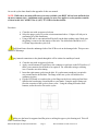
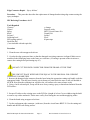
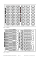
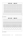
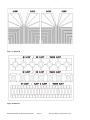
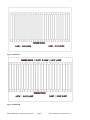
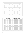
Introduction The knowledge and skills needed for PCB repair are practiced and taught daily by BEST Inc. The procedures in this instruction manual comply with the IPC-the governing body dealing with the standards for printed circuit board manufacturing. These standards include the following J-STD-001 IPC-7711 IPC-7721 IPC-610 IPC-600 Requirements for Soldered Electrical Connections Rework of Electronic Assemblies Repair and Modification of Printed Boards and Assemblies Acceptability of Electronic Assemblies Acceptability of Printed Boards General handling guidelines for printed circuit boards are applicable to any rework or repair done to PCBs. These guidelines are referred to in the following: 1. 2. 3. 4. 5. Electronic components and assemblies need to be handled and cared for per the J-STD033 MSD guidelines IPC-A-610 IPC 7721 Section 2.1 Handling Electronic Assemblies Proper Care for Electrostatic Discharge (ESD) Proper Care for EOS Electrical Overstress (EOS) Why BEST Inc Repair Kits? BEST repair kits feature the right “tools of the trade” selected by BEST Inc repair technicians who have repaired thousands of PCBs over the years. For instance, “tools of the trade” such as dental pics are great for digging out burnt PCB laminate materials and are included in our standard PCB repair kit. Compare the number of patterns available on BEST frames with those of other manufacturers and you will agree that you get more for your money with BEST circuit frames. You will get MORE repairs out of BEST circuit frames. Easy to follow instructions including “how to” photos allows you to more accurately repeat the procedures followed by professional PCB repair instructors and technicians. Instruction, either through a video medium or in person, is available from an IPC master instructor in 7721 procedures Repair procedures are highly labor intensive and as such rely on the individual skills of the operator. Repair of printed circuit boards is based on the experience of the operators and should not be performed by personnel who are only performing the repairs a few hours per week or on a rotational basis with other job functions. PCB repairs are highly specialized requiring the skill, caring and creativity normally found and practiced by artisans. Compliance of products to IPC Procedures Most of the products herein are designed to comply with procedures referenced in IPC 7721 Modification and Repair of Printed Boards and Assemblies BEST PCB Repair Kit Instructional Booklet Page 1 Revision Dated 2/9/2010 Version 1.0 Table of Contents Section Pages Introduction…………………………………………………1 Trace Repair-Epoxy Method…………….………………...3-4 Trace Repair-Dry Film Method…………….……………...5-6 Plated Hole Repair…………………………………………7-9 Lifted Pad Repair…………………………………….……. 10 Edge Connector Repair-Epoxy Method…………………..11-12 Edge Connector Repair-Dry Film Method……………….13-14 Base Board Repair………………………………………….15 Solder Mask Repair…………………………………………16 Damaged Corner or Laminate Edge Repair…..…………...17 Gold Replating ………………..……..…………...………18-20 Epoxy Mixing and Curing………………………………….21 Repair Kits Available……………………………………..22 Accessories/Spares……………………………………...23-47 References…………………………………………….…….48 BEST PCB Repair Kit Instructional Booklet Page 2 Revision Dated 2/9/2010 Version 1.0 Trace Repair –Epoxy Method Procedure: This procedure is designed to repair damaged SMT land/trace combinations using the epoxy method. The traces you cut from the BEST circuit frame library are joined to existing printed circuit board traces. IPC Referring Procedures: IPC 7721 4.2.1 Tools Required Small c-clamps Cleaning solvent* BEST Circuit Frame #3A BEST epoxy Kapton tape* Knife ESD-safe cutting surface* Orange sticks (* not included with standard repair kit) Flux* Microscope* Dental pics Solder* Soldering Iron* Wipes* Popsicle sticks Procedure a. Clean the area with an approved solvent. b. Remove the damaged circuitry from the board utilizing the cutting knife supplied in the repair kit. The damaged conductor should be trimmed on the PCB to a point where it is still wellbonded to the PCB. Heat can be applied to the damaged conductor using a soldering iron to allow the trace to be removed more easily c. Clean any excess solder off the existing trace for a distance of 2-3 trace widths.. Apply flux and tin this area. d. Clean the board with an approved solvent. e. Match up the trace from the BEST Frame. Be sure to remember the identifying letter or number on the circuit frame for any further procedures which may be required For custom sizes use a knife to trim the proper trace from the circuit frame of call BEST (847) 797-9250 for custom trace requirements. DO NOT CUT THE SELECTED REPLACMENT CIRCUIT AT THIS TIME f. Scrape the excess oxides from the copper surface where you will be lapping to the existing circuit trace g. Cut the replacement circuitry from the frame using the knife provided. Do not stretch or damage the trace prior to placement. BEST PCB Repair Kit Instructional Booklet Page 3 Revision Dated 2/9/2010 Version 1.0 h. Position the replacement trace section at the proper location. If necessary bend the trace using the orange sticks as needed to match the shape of the existing conductor. Wooden sticks can be used to help bend the new traces. Use one orange stick to hold the new trace at the location of the bend while using the other to bend the other wood stick to form the shape as needed. For wider traces you may need to fold over the trace to produce sharp bends. k. Form the final trace shape holding it into place with ESD-safe tape. l. Apply flux and form a lap solder joint at the overlap. Remove the tape. m. Mix the epoxy. Coat the bottom of the trace with epoxy using the ends of the wooden orange sticks. In order to continue to apply even pressure over the bonded area use the appropriate small c-clamp and popsicle sticks. Cut and stack the sticks on both sides of the PCB. Clamp against these popsicle stick wedges to apply firm even pressure over the bond area. Be careful to not apply too much pressure as components and coatings can be crushed. n. o. p. q. Cure the epoxy per the manufacturer’s directions Clean the repair area with an approved solvent. Apply any coating to the board that was previously existent. Visually examine the repair. Tape test as per IPC-TM-650 (ANSI/IPC-FC-250A) test method 2.4.1. r. Visually examine the proper alignment of the trace and the overlap of the trace. s. Visually examine the area of the epoxy coating for texture matches. t. Test the site for electrical continuity as applicable. BEST PCB Repair Kit Instructional Booklet Page 4 Revision Dated 2/9/2010 Version 1.0 Trace Repair –Dry Film Method Procedure: This procedure is designed to repair damaged SMT land/trace combinations using the dry film method. The traces you cut from the BEST circuit frame library are joined to existing printed circuit board traces. IPC Referring Procedures: IPC 7721 4.5.2????? Tools Required Small c-clamps Cleaning solvent* BEST Circuit Frame #3ADF BEST epoxy Kapton tape* Knife ESD-safe cutting surface* Orange sticks (* not included with standard repair kit) Flux* Microscope* Dental pics Solder* Soldering Iron* Wipes* Popsicle sticks Bonding iron and tips* Procedure i. Clean the area with an approved solvent. j. Remove the damaged circuitry from the board utilizing the cutting knife supplied in the repair kit. The damaged conductor should be trimmed on the PCB to a point where it is still wellbonded to the PCB. Heat can be applied to the damaged conductor using a soldering iron to allow the trace to be removed more easily k. Clean any excess solder off the existing trace for a distance of 2-3 trace widths.. Apply flux and tin this area. l. Clean the board with an approved solvent. m. Match up the trace from the BEST dry film adhesive frame. Be sure to remember the identifying letter or number on the circuit frame for any further procedures which may be required For custom sizes use a knife to trim the proper trace from the circuit frame of call BEST (847) 797-9250 for custom trace requirements. DO NOT CUT THE SELECTED REPLACMENT CIRCUIT AT THIS TIME n. Scrape the excess oxides from the copper surface where you will be lapping to the existing circuit trace o. Cut the replacement circuitry from the frame using the knife provided. BEST PCB Repair Kit Instructional Booklet Page 5 Revision Dated 2/9/2010 Version 1.0 Do not stretch or damage the trace prior to placement. p. Position the replacement trace section at the proper location. If necessary bend the trace using the orange sticks as needed to match the shape of the existing conductor. Wooden sticks can be used to help bend the new traces. Use one orange stick to hold the new trace at the location of the bend while using the other to bend the other wood stick to form the shape as needed. For wider traces you may need to fold over the trace to produce sharp bends. k. Form the final trace shape holding it into place with ESD-safe tape. u. Apply flux and form a lap solder joint at the overlap. Remove the tape. v. Select the proper bonding tip with the shape matching the new trace as closely as possible. w. Place the bonding tip directly on to the new trace pattern. Apply pressure as recommended for approximately 30 seconds. After this bonding operation has been completely remove the tape used for alignment. x. Clean the repair area with an approved solvent. y. Apply any coating to the board that was previously existent. z. Visually examine the repair. Tape test as per IPC-TM-650 (ANSI/IPC-FC-250A) test method 2.4.1. aa. Visually examine the proper alignment of the trace and the overlap of the trace. bb. Visually examine the area of the epoxy coating for texture matches. cc. Test the site for electrical continuity as applicable. BEST PCB Repair Kit Instructional Booklet Page 6 Revision Dated 2/9/2010 Version 1.0 Via Repair-see “PlatedHole Instructions” instructional slides Procedure: This procedure is designed to repair damaged vias/holes with no interlayer connections. Damage to the hole is repaired with an eyelet with the eyelet flanges replacing the pads on the PCB. IPC Referring Procedures: IPC 7721 5.1 Tools Required Caliper* Cleaning solvent* Knife Eyelet kit Eyelet forming tools Soldering Iron* Hammer Flux* Microscope* Drill Press or hand drill* Wipes* Solder* Drill bits or ball mills* (* not included with std repair kit) Choosing the right eyelet for the repair: FD ID OD LUF Chose the proper eyelet keeping the following in mind: LUF The length of the eyelet barrel under the flange should be 0.630-0.890mm greater than the thickness of PCB(this allows the for the right length after the flange is formed) ID Eyelet inside diameter should be 0.075-0.500mm greater than the component lead diameter for proper fit of the through-hole component lead. FD The flange diameter should be sized so that it does not protrude out onto other pads or conductors in the vicinity OD The clearance in the PCB hole should allow the eyelet to be inserted without undue force but, but should not exceed 0.125mm greater than the eyelet outside diameter. BEST PCB Repair Kit Instructional Booklet Page 7 Revision Dated 2/9/2010 Version 1.0 Or use the eyelet chart found in the appendix of this user manual. NOTE: While there are many different eyelet sizes available your BEST kit has been outfitted with the most common sizes. A minimum order quantity for new sizes applies to eyelet purchase outside of those in this kit. Call BEST Inc @ (847) 797-9250 for further details. Procedure a. Clean the area with an approved solvent. b. Select the proper eyelet as per the criteria mentioned above. Calipers will aid you in confirming all of the dimensions c. Using a ball mill or conventional drill bit, drill out the hole needing repair. Make sure the plating is removed on the interior of the hole. The drilled hole should be 0.025 – 0.125mm larger than the eyelet O.D. Drill should enter from the undamaged side of the PCB to exit on the damaged side. This prevents further PCB damage. Any internal connections to the plated throughole will be isolated on multilayer boards d. Clean the area with an approved solvent. e. Apply a small amount of liquid flux to the conductor or pad area on the PCB surface (if there is one connected to the hole to be repaired). Tin with solder using a soldering iron. Clean the area after tinning. f. Insert the replacement eyelet into the hole. If a replacement conductor is required it may extend into the drilled hole. The flange of the new eyelet will hold the new conductor in place. g. Flip the PCB board over and rest the eyelet flange on the lower setting tool/tool base. Stabilize the board using a board holder or your hands. Using the upper flaring tool flare the extension of the eyelet to form a cone. Using the setting tool and a small hammer, strike the tool to flat set the eyelet. Make sure the board is supported and flat prior to striking the upper eyelet forming tool. This will insure a uniform flange. BEST PCB Repair Kit Instructional Booklet Page 8 Revision Dated 2/9/2010 Version 1.0 Inspect eyelet per IPC 610 Acceptability Criteria h. Apply a small amount of liquid flux and solder the eyelet flanges to the pads of the PCB if necessary. The solder should go up 75% of the height of the flared flange. Clean the area. Inspect for a good solder connection. It should be properly wetted and should have flowed to the proper areas. i. Inspect the pad diameter both inside and outside. j. Make any electrical continuity measurements BEST PCB Repair Kit Instructional Booklet Page 9 Revision Dated 2/9/2010 Version 1.0 Lifted Pad Repair- see “Pad Trace Instructions” instructional slides Procedure: This procedure describes how to rebond a lifted conductor using the epoxy technique. Liquid epoxy is inserted under and around the conductor in order to bond it back down to the PCB surface. IPC Referring Procedures: IPC 4.1.1. Tools Required Cleaning Solvent* Wipes* Epoxy Knife Dental Pick Kapton 2” wide tape* c-clamp Popsicle sticks (* not included with std repair kit) Procedure a. Clean the area with an approved solvent. b. Remove any items preventing the lifted conductor from making contact with the base PCB material c. Clean the area with an approved solvent d. Mix the epoxy per the specified instructions 1. Before mixing, prepare surfaces to be clean, dry and free of oil, grease or wax. 2. Mix both resin and hardener on a clean, dry, flat surface which can later be discarded. 3. Squeeze an even amount of Resin and Hardener parallel to each other onto the mixing surface. 4. Mix thoroughly until both the Resin and Hardener blend into one uniform color 5. Apply adhesive within 50 minutes after mixing. e. Carefully apply a small amount of epoxy under the entire lifted area of the conductor. Use either a knife tip or a small orange stick to get the epoxy underneath the conductor area. f. Press the lifted pad or conductor down into the epoxy and into contact with the base PCB material g. Apply additional epoxy to the surface of the lifted pad/conductor and to all sides as needed In order to continue to apply even pressure over the bonded area use the appropriate small c-clamp and popsicle sticks. Cut and stack the sticks on both sides of the PCB. Clamp against these popsicle stick wedges to apply firm even pressure over the bond area. Be careful to not apply too much pressure as components and coatings can be crushed. h. Cure the epoxy per the instructions i. If there was previously a surface coating, re-apply the same coating dd. Visually examine the repair. Tape test as per IPC-TM-650 (ANSI/IPC-FC-250A) test method 2.4.1. j. Make appropriate electrical tests. BEST PCB Repair Kit Instructional Booklet Page 10 Revision Dated 2/9/2010 Version 1.0 Edge Connector Repair – Epoxy Method Procedure: This procedure describes the replacement of damaged and missing edge contacts using the epoxy technique. IPC Referring Procedures: 4.6.2 Tools Required Cleaner* Wipes* Epoxy Knife Solvent* Soldering Iron* ESD cutting surface* Small flat file* (* not included with std repair kit) c-clamps Popsicle sticks BEST Circuit Frame #2A Dental Pick Solder* Flux* Kapton tape Procedure 1. Clean the area with an approved solvent. 2. Overlay the edge connector frame so that the damaged or missing connector is aligned. Make sure to mark down the identifying letter on the frame as a reference. (If coating is present on the circuit trace , remove the coating before performing step #3) DO NOT CUT THE EDGE CONNECTOR FROM THE FRAME AT THIS TIME’ THE CIRCUIT TRACE WIDTH MUST BE EQUAL TO THE ORIGINAL FOR CURRENT HANDLING CAPABILTIIES 3. Remove the damaged edge connector from the board using the appropriate cutting tool handle (with the appropriate blade). Trim the trace from the circuit frame to a point where the trace is still well bonded to the PCB. Heat from the soldering iron will allow the old contact to be removed more easily 4. Using a knife or dental pick, scrape off the area of any coating, epoxy or burnt board material from the PCB surface 5. Scrape off oxides on the existing trace on the PCB for a length of at least 3 trace widths using the knife to remove any oxides and mask. Tin the trace end by first fluxing the area and then applying solder. 6. Clean the board using an approved solvent. 7. Cut the replacement edge connector (with trace) from the circuit frame BEST #2. Use the cutting tool handle and an ESD safe cutting surface. BEST PCB Repair Kit Instructional Booklet Page 11 Revision Dated 2/9/2010 Version 1.0 8. Position the replacement edge connector at the proper location. The area where the new connector will be placed should be flat and smooth. If NOT then refer to other laminate repair procedures. Kapton tape can be used at the replacement edge connector in order to properly hold it into position. The trace overlap should be at least 2 times the circuit trace width. In order to continue to apply even pressure over the bonded area use the appropriate small c-clamp and popsicle sticks. Cut and stack the sticks on both sides of the PCB. Clamp against these popsicle stick wedges to apply firm even pressure over the bond area. Be careful to not apply too much pressure as components and coatings can be crushed. 9.Mixing and Preparing the epoxy 1. Before mixing, prepare surfaces to be clean, dry and free of oil, grease or wax. 2. Mix both resin and hardener on a discardable, clean, dry, flat surface. 3. Squeeze an even amount of Resin and Hardener parallel to each other onto the mixing surface. 4. Mix thoroughly until both the Resin and Hardener blend into one uniform color 5. Apply adhesive within 50 minutes after mixing. 10.Apply a small amount of epoxy to the surface where the new contact will be placed. Place the trace onto the PCB. 11. After the epoxy has cured, remove any tape that was used. Inspect for placement. Chamfer the edge of the replacement edge connector with a file. This will help provide a smooth surface while lessening edge damage not causing the edge connector. ADDITONAL EPOXY CAN BE APPLIED TO THE PERIMETER OF THE NEW EDGE CONTACT TO PROVIDE BOND STRENGTH. 12. Flux the area where the trace is attached to the PCB. Create a lap joint by soldering the circuit traces together overlapping one with the other. 13. Clean the area with an approved solvent. 14. If sealing of the lap joint is required, coat the lap solder joint solder connections with solder mask. 15. If plating is required refer to the appropriate procedures. 16. Examine visually. Confirm pad and trace dimensions. 17. Check electrical continuity BEST PCB Repair Kit Instructional Booklet Page 12 Revision Dated 2/9/2010 Version 1.0 Edge Connector Repair – Dry Film Method Procedure: This procedure describes the replacement of damaged and missing edge contacts using the dry film technique. IPC Referring Procedures: 4.6.2 Tools Required Cleaner* Wipes* Bonding Iron/Tips* Knife Solvent* Soldering Iron* ESD cutting surface* Small flat file* (* not included with std repair kit) c-clamps Popsicle sticks BEST Circuit Frame #2ADF Dental Pick Solder* Flux* Kapton tape Procedure 1. Clean the area with an approved solvent. 2. Overlay the edge connector frame so that the damaged or missing connector is aligned. Make sure to mark down the identifying letter on the frame as a reference. (If coating is present on the circuit trace , remove the coating before performing step #3) DO NOT CUT THE EDGE CONNECTOR FROM THE FRAME AT THIS TIME’ THE CIRCUIT TRACE WIDTH MUST BE EQUAL TO THE ORIGINAL FOR CURRENT HANDLING CAPABILTIIES 3. Remove the damaged edge connector from the board using the appropriate cutting tool handle (with the appropriate blade). Trim the trace from the circuit frame to a point where the trace is still well bonded to the PCB. Heat from the soldering iron will allow the old contact to be removed more easily 4. Using a knife or dental pick, scrape off the area of any coating, epoxy or burnt board material from the PCB surface 5. Scrape off oxides on the existing trace on the PCB for a length of at least 3 trace widths using the knife to remove any oxides and mask. Tin the trace end by first fluxing the area and then applying solder. 6. Clean the board using an approved solvent. 7. Cut the replacement edge connector (with trace) from the circuit frame BEST #2ADF. Use the cutting tool handle and an ESD safe cutting surface. BEST PCB Repair Kit Instructional Booklet Page 13 Revision Dated 2/9/2010 Version 1.0 8. Position the replacement edge connector at the proper location. The area where the new connector will be placed should be flat and smooth. If NOT then refer to other laminate repair procedures. Kapton tape can be used at the replacement edge connector in order to properly hold it into position. The trace overlap should be at least 2 times the circuit trace width. 9.Match up the edge connector from the BEST dry film adhesive frame. Be sure to remember the identifying letter or number on the circuit frame for any further procedures which may be required For custom sizes use a knife to trim the proper edge connector from the circuit frame or call BEST (847) 797-9250 for custom edge connector requirements. DO NOT CUT THE SELECTED REPLACMENT CIRCUIT AT THIS TIME 11. Remove any tape that was used. Inspect for placement. Chamfer the edge of the replacement edge connector with a file. This will help provide a smooth surface while lessening edge damage not causing the edge connector. ADDITONAL EPOXY CAN BE APPLIED TO THE PERIMETER OF THE NEW EDGE CONTACT TO PROVIDE BOND STRENGTH. 12. Flux the area where the trace is attached to the PCB. Create a lap joint by soldering the circuit traces together overlapping one with the other. 13. Clean the area with an approved solvent. 14. If sealing of the lap joint is required, coat the lap solder joint solder connections with solder mask. 15. If plating is required refer to the appropriate procedures. 16. Examine visually. Confirm pad and trace dimensions. 17. Check electrical continuity BEST PCB Repair Kit Instructional Booklet Page 14 Revision Dated 2/9/2010 Version 1.0 Base Board RepairProcedure: This procedure describes how to “fill” holes, gouges or large scratches in the PCB laminate. Liquid epoxy is selectively filled in to areas of the PCB where scratches, holes, gouges are located. IPC Referring Procedures: IPC 7711 4.1.1. Tools Required Cleaning Solvent* Wipes* Epoxy Knife Dental Pick Ball mill, large and small* (* not included with std repair kit) Kapton 2” wide tape* c-clamp Popsicle sticks Scraper* Hand drill* Procedure 1. Clean the area with an approved solvent. 2. Remove any components or materials preventing access to the area requiring repair. 3. Clean the area with an approved solvent 4. Remove the laminate or any sharp edges or exposed fibers on the corner of that laminate 5. Use oversized ball mill to remove any signs of the damaged or charred laminate. Follow this with a smaller ball mill to “smoothen out” the edges of the repair 6. Use a scraper to “flatten out” the bottom of the hollowed out area of the removed area such that it is parallel to the surface of the laminate 7. Clean the area with an approved solvent 8. Prepare the two-part epoxy resin supplied as per the instructions. a. Before mixing, prepare surfaces to be clean, dry and free of oil, grease or wax. b. Mix both resin and hardener on a discardable, clean, dry, flat surface. c. Squeeze an even amount of Resin and Hardener parallel to each other onto the mixing surface. d. Mix thoroughly until both the Resin and Hardener blend into one uniform color e. Prepare the color of the epoxy using the color agents provided (if required) f. Apply adhesive within 50 minutes after mixing. 9. Cure the epoxy as per the manufacturers' guidelines. It will dry somewhat concave (protruding from the surface of the circuit board) NOTE: Protect heat sensitive components or remove them prior to heat curing the epoxy 10. Wet sand with a fine grit emery paper 11. Apply butter coat finish. Use some of the epoxy /resin previously mixed and add a small amount of isopropyl alcohol to the mixture. Mix this in with the epoxy/resin compound. Apply a “skim coat” or very thin layer to the top of the PCB in order to smooth out the surface finish. 12. If there was previously a surface coating, re-apply the same coating 13. Visually examine the repair. 14. Make appropriate electrical tests. BEST PCB Repair Kit Instructional Booklet Page 15 Revision Dated 2/9/2010 Version 1.0 Solder Mask Repair Procedure: The procedure described below is used to replace solder mask on printed circuit boards. The repair uses the brushing technique to apply the repair material. IPC Referring Document: IPC 7721 2.4.1 Cleaning Solvent* Drill bits or ball mills * Color agent, variety of colors* Epoxy Kapton tape* Utility knife Microscope* Oven* Wipes* (* not included with std repair kit) Procedure 1. Clean the damaged area with an approved solvent NOTE: This repair method can only be used for surface damages or those into the base board material. However, this method should not be used when the damage is completely through the board. 2. Remove the laminate or any sharp edges or exposed fibers on the corner of the laminate NOTE: In order to make sure all of the damaged laminate and PCB solder mask are “seen”, flood the area being repaired with alcohol. If any of the PCB internal fibers are damaged, then they will likely show up at this time. 3. Clean the area with an approved solvent 4. Apply Kapton tape to protect the parts of the PCB that need protection and as a “mask” to the area being repaired. 5. Prepare the two-part epoxy resin supplied as per the instructions. 6. Mix the epoxy per the specified instructions a. Before mixing, prepare surfaces to be clean, dry and free of oil, grease or wax. b. Mix both resin and hardener on a clean, dry, flat surface which can later be discarded. c. Squeeze an even amount of Resin and Hardener parallel to each other onto the mixing surface. d. Prepare the color of the epoxy using the color agents provided (if required) e. Mix thoroughly until both the Resin and Hardener blend into one uniform color 7. Apply adhesive within 50 minutes after mixing. 8. Cure the epoxy as per the manufacturers' guidelines. It will dry somewhat concave (protruding from the surface of the circuit board) NOTE: Protect heat sensitive components or remove them 9. Remove the Kapton tape 10. If there was previously a surface coating, re-apply the same coating 11. Visually examine the repair. Tape test as per per IPC-TM-650 (ANSI/IPC-FC-250A) test method 12. Make appropriate electrical tests. BEST PCB Repair Kit Instructional Booklet Page 16 Revision Dated 2/9/2010 Version 1.0 Damaged Corner or Laminate Edge Repair Procedure: This procedure describes how to repair a damaged PCB laminate edge or corners. These damages are usually the result of handling or packaging damage. IPC Referring Document: IPC 7721 3.5.3 Tools Required: Cleaning solvent* Drill bits or ball mills* Color agent, variety of colors* Epoxy Hand-held drill* Kapton tape* (* not included with std repair kit) Utility knife Microscope* Oven* Scraper* Wipes* Plastic box* Procedure 1. Clean the area with an approved solvent Remove any items preventing you from having complete access to area requiring repair. 2. Remove the laminate or any sharp edges or exposed fibers on the corner of that laminate 3. Find a small plastic box such as used in holding electronic components. All you will need is a single corner of the box matching the peripheral lengths of the corner area of the PCB. 4. Align the PCB with the damaged corner “nestled into” the corner of the plastic box. Make sure to align these edges. Fixture or tape the PCB into place. 5. Mix the epoxy per the specified instructions a. Before mixing, prepare surfaces to be clean, dry and free of oil, grease or wax. b. Mix both resin and hardener on a clean, dry, flat surface which can later be discarded. c. Squeeze an even amount of Resin and Hardener parallel to each other onto the mixing surface. d. Mix thoroughly until both the Resin and Hardener blend into one uniform color e. Add colorant if required f. Apply adhesive within 50 minutes after mixing. 6. Backfill the mixed epoxy into the corner of the box until the level of the epoxy is even with the level of the PCB laminate surface. 7. Cure the epoxy as per the manufacturers' guidelines. It will dry somewhat concave (protruding from the surface of the circuit board) NOTE: Protect heat sensitive components or remove them 8. Wet sand with a fine grit Emory paper 9. Apply butter coat finish. This is done by taking some of the epoxy /resin previously mixed and adding a small amount of isopropyl alcohol to the mixture. Mix this in with the epoxy/resin compound. Apply a “skim coat” or very thin layer to the top of the PCB in order to smooth out the surface finish. 10. Clean the repair area using isopropyl alcohol 11. Dry with antistatic wipes 12. Visually inspect 16. Make the appropriate electrical test BEST PCB Repair Kit Instructional Booklet Page 17 Revision Dated 2/9/2010 Version 1.0 Gold Finger Replating Procedure: This procedure is designed to replate gold edge contacts by selective brush plating via a clean, preloaded pen system. When edge contacts are scratched or become “splashed” with excess solder or they do not meet the minimum thickness specifications they need to be replated. This electroplating process uses an easy-to-use cleaning and replating system. It includes a miniature variable DC power supply. One lead is connected to the connector edge contacts that need plating. A second lead is connected to the plating pen. These pens have the metallic cleaning or plating material in solution in a swab tip where solution is absorbed into the tip. When the top of this pen is swabbed across the edge connector contacts the material contained in the tip of the pen is plated wherever electrical contact has been made. All areas to be plated need to be prepared such that any contamination is removed. IPC Referring Procedures: IPC 7721 4.6.3 Tools Required Rinse bottle* Microscope* Solder wick* Dental pics* Work sink* Solder* Wipes * Soldering Iron* Safety Glasses * Wipes* Peel testing tape Absorbent pen Cleaning solvent* Nickel pen Gold pen Power supply with 2 integrated cables Cerium oxide Water (* not included with standard repair kit) Procedure q. Clean the area with an approved solvent. r. Make sure all of the contact areas have been wicked using a soldering iron and braid such that the surfaces to be replated are flat. s. Plug the power supply in and switch output voltage to 10 V for the absorbent pen. The absorbent pen is designed to provide a clean, residue and oxide free surface. t. Touch the contact probe end (BLACK - ) to the inboard edge of each contact being replated or to the connecting circuit as each pen tipped metal is applied to during the plating process. The pen end will be applied to where the plating material needs to be added. Using the cleaning pen (PP1) attached to the (red) probe, clean the entire surface which will be replated. Clean by moving the service end of the pen over the area back and forth. Once dry, burnish all small imperfections from the surface to be replated using a lint free cloth and a cerium oxide mixture. Mix water with cerium oxide until it has a milky consistency. Buff the contacts unit all defective or poor plating is removed. Wait until the liquids seeps into the ends of the pen. Do not shake the pen in order to try to get the material down into the swab tip of the pen. BEST PCB Repair Kit Instructional Booklet Page 18 Revision Dated 2/9/2010 Version 1.0 Thoroughly rinse the entire area with water until all of the residue is removed. A conductive bus must be made to all contacts that need plating. While there are other connection options the above method produces the highest quality replating. For other connection methods call BEST (847) 797-9250. The plating process u. Plug the power supply into the proper outlet. Make sure the output voltage setting is correct as given in the chart in this manual. Set the power supply to 6 V for the nickel pen. v. Make the connection to the circuit board. Touch the contact probe end to the inboard edge of each contact being replated or to the connecting circuit as previous. w. Connect the nickel plating material pen to the red cable. Swab the entire surface to be plated by brushing the surface with the pen. The plating pen should be moved back and forth briskly to prevent burning and to provide even coverage. Refer to the plating thickness vs time chart in this manual for approximate coating thickness. Reattach the pen cap when this step is completed. Disconnect the nickel plating pen. Unplug the power supply. x. Buff with the powder slurry provided as previously described. Rinse the contact pads thoroughly with water. y. Connect the gold plating material pen to the red cable. Plug the power supply into the outlet. Set the output voltage of the power supply to 8V. Swab the entire surface to be plated by brushing the surface with the pen. The plating probe should be moved back and forth briskly to prevent burning and to provide even coverage. Refer to the plating thickness vs time chart in this manual for approximate coating thickness. Reattach the pen cap when this step is completed. Disconnect the gold plating pen. z. Buff with the powder slurry as previously described. Rinse the contact pads. aa. Rinse thoroughly with water. bb. Evaluate/inspect the replating area i. Measure the nickel and gold thicknesses via the proper measuring equipment ii. Using IPC TM-650 check the peel strength of the plating material using the peel tape test a. Use 3M brand 600 tape ½” in width b. Apply 50 mm length of tape to plated area. Make sure all entrapped air out from underneath the tape. The time from application until the peel test shall be less than 1 minute. The strip must be unused to perform this test c. Remove the tape by rapid perpendicular pull force relative to the board. BEST PCB Repair Kit Instructional Booklet Page 19 Revision Dated 2/9/2010 Version 1.0 d. Visually examine tape and test area for any remnant plating material. Remnants on either shall be a fail. iii. Examine the rework area for color and luster at 1.75x magnification. iv. Inspect the surrounding area for any defects a. Make sure the coverage is complete and the finish is uniform on the surface to be plated. No extraneous plating or nickel foot or edge pull back nor skip plating shall be on the plated surfaces (See IPC A610 Acceptability Requirements) b. The nickel thickness shall be between 3 and 6 um (118.1 to 236.2 ư in) c. Gold thickness shall be a minimum of 0.05um (1.97 ư in). The typical range is 0.075 to 0.125 um (2.955 to 4.925 ư in of gold) v. Test the site for electrical continuity as applicable. Plating Time - s Contact Area vs Plating Time 35 30 25 20 15 10 5 0 Nickel Gold 5 10 15 20 25 Contact Area - sq mm Recommended Output Voltage for Each of Plating Pens BEST P/N PP1 PP2 PP3 Description Absorbent Pen Gold-24K Nickel Voltage 10-12V 6-8V 5-6V BEST PCB Repair Kit Instructional Booklet Usage Cleaning of metals prior to plating Plating over gold and nickel Plating over copper Page 20 Revision Dated 2/9/2010 Version 1.0 Epoxy Curing Instructions Procedure: The BEST 2-part epoxy is used to adhere replacement pads, traces and lads to the PCB as well as being used as a media for the repair of the PCB base. The epoxy system has been used for 20 plus years and features: a clear color, room temp or heat cure and is easy to mix. Tools Required: Premixed epoxy/resin package Flat plate for mixing epoxy Orangewood stick for mixing epoxy Dental pick or other device for applying mixed epoxy to small areas Procedure 1. Clean the area with an approved solvent. Make sure it is dry. Remove any items preventing you from having complete access to the area requiring repair. 2. Combine the Resin and the hardener in the correct ratio and mix thoroughly until the color and consistency are uniform. EQUAL BEAD LENGTHS OF BOTH THE RESIN AND HARDNER WILL GIVE YOU THE RIGHT RATIO! Mixing the adhesive just prior to use is recommended Heat build up during or after mixing is normal. Mixing smaller quantities will minimize the heat buildup. 3. The bonded parts should be held in contact until the part has developed holding strength. 4. This adhesive system can be completely cured with heat such as 2 hours at 60ºC (140ºF), 1 hour at 60ºC (180º F) of 30 minutes at 121ºC (250º F). Heat cures can be used to achieved a desired degree of cure from handling strength to the full cure. After 24 hours at room temperature 90% of the full cure properties are obtained. The parts will be completely cured after 3 days at room temperature. Store the epoxy elements in an unopened container in a cool dry location. Ideal storage conditions are between 8 and 21º C (46 to 70º F). Exposure to temperatures over 28ºC (82º F) for prolonged periods should be avoided as this can adversely impact product properties. BEST PCB Repair Kit Instructional Booklet Page 21 Revision Dated 2/9/2010 Version 1.0 PCB REPAIR KITS AVAILABLE BEST PCB Repair Kit BEST PCB repair kits give you the tools you need for fast repair and modification of lands, traces, contact fingers, SMT pads, plated hole connections and PCB base board material. These materials, packaged together and designed by one of the premier PCB repair companies, BEST Inc., allow you to meet original PCB quality standards. Both dry film and epoxy circuit frames are available. BEST Circuit Trace Repair Kit BEST PCB circuit trace repair kit give you the tools you need for fast repair and modification of circuit traces. These materials, packaged together and designed by one of premier PCB repair companies, BEST Inc, allows you to meet original PCB quality standards BEST Epoxy Repair Kit This kit contains 10 packages of clear, low viscosity, superior strength epoxy, precisely measured out into two-compartment plastic packages so it’s easy to use and there’s no measuring. Once cured, this epoxy makes an effective electrical insulator with good high temperature mechanical and impact resistance properties. The epoxy can be used to fill in holes, gaps, burns or to inject into delaminated locations. The kit also contains mixing sticks, mixing cups and foam swabs. BEST Baseboard Repair Kit The BEST baseboard repair kit gives you the tools to repair nearly all types of base board defects including impact damage, burns, delamination, blistering, measling, warp, routing errors and more. We can also repair defects in coatings, solder mask and legend BEST Solder Mask Repair Kit The BEST solder mask repair kit gives you all of the supplies you need to repair damaged solder mask. BEST Plated hole Repair Kit Here are all the tools and materials you'll need to repair damaged plated holes in circuit boards. Kit includes 8 different sizes of eyelets. BEST Pad Repair Kit This kit includes everything you need to reliably replace damaged surface mount and BGA pads. The replacement pads use the epoxy technique. Both dry film and epoxy circuit frames are available. BEST Land Repair Kit You'll find the solution in this kit specifically designed to make the process of land repair as simple and effective as possible. Both dry film and epoxy circuit frames are available. BEST Gold Replating Kit In this kit you will find all of the necessary materials for the replating of gold plated contact fingers and gold plated areas. BEST PCB Repair Kit Instructional Booklet Page 22 Revision Dated 2/9/2010 Version 1.0 ACCESSORY PARTS/SPARES Part Number ResinHarnerforPCBRepKit2gm PopSickleStickWood-10 OrangeStickWood-10 SwageToolBase SwageToolFixture Eylt021030078-100 Eylt034046093-100 Eylt058068102-100 Eylt076040093-100 Eylt064076091-100 Eylt048059093-100 BEST1ACktTrack BEST1BCktTrack BEST1CCktTrack BEST1ACktTrackDF BEST1BCktTrackDF BEST1CCktTrackDF BEST2ACktTrack BEST2BCktTrack BEST2ACktTrackDF BEST2BCktTrackDF BEST3ACktTrack BEST3BCktTrack BEST3ACktTrackDF BEST3BCktTrackDF BEST4ACktTrack BEST4BCktTrack BEST4ACktTrackDF BEST4BCktTrackDF BEST5ACktTrack BEST5BCktTrack BEST5CCktTrack BEST5ACktTrackDF BEST5BCktTrackDF BEST5CCktTrackDF BEST6ACktTrack BEST6BCktTrack BEST6ACktTrackDF BEST6BCktTrackDF BEST7ACktTrack BEST7BCktTrack BEST7CCktTrack BEST7ACktTrackDF BEST7BCktTrackDF BEST7CCktTrackDF BEST8ACktTrack BEST PCB Repair Kit Instructional Booklet Description Resin/Hardner, 2gms with divider Popsicle sticks for clamping down for PCB repairs, 10 count Orange sticks for mixing, 10 count Swaging tool for through hole repairs-base Swaging tool for through hole repairs-fixture Eyelet .021" ID, .030" OD, .078" LUF 100 pcs Eyelet .034" ID, .046" OD, .093" LUF 100 pcs Eyelet .058" ID, .068" OD, .102" LUF 100 pcs Eyelet .076" ID, .040" OD, .093" LUF 100 pcs Eyelet .064" ID, .076" OD, .091" LUF 100 pcs Eyelet .048" ID, .059" OD, .093" LUF 100 pcs Surface Mount Pad Circuit Frame, tin plated, for epoxy use Surface Mount Pad Circuit Frame, tin plated, for epoxy use Surface Mount Pad Circuit Frame, tin plated, for epoxy use Surface Mount Pad Circuit Frame, tin plated, for dry film Surface Mount Pad Circuit Frame, tin plated, for dry film Surface Mount Pad Circuit Frame, tin plated, for dry film Edge Connector Circuit Frame, tin plated, for epoxy use Edge Connector Circuit Frame, tin plated, for epoxy use Edge Connector Circuit Frame, tin plated, for dry film Edge Connector Circuit Frame, tin plated, for dry film SMT Trace Circuit Frame, tin plated, for epoxy use SMT Trace Circuit Frame, tin plated, for epoxy use SMT Trace Circuit Frame, tin plated, for dry film SMT Trace Circuit Frame, tin plated, for dry film Through Hole Circuit Frame, tin plated, for epoxy use Through Hole Circuit Frame, tin plated, for epoxy use Through Hole Circuit Frame, tin plated, for dry film Through Hole Circuit Frame, tin plated, for dry film BGA Pad Circuit Frame, tin plated, for epoxy use BGA Pad Circuit Frame, tin plated, for epoxy use BGA Pad Circuit Frame, tin plated, for epoxy use BGA Pad Circuit Frame, tin plated, for dry film BGA Pad Circuit Frame, tin plated, for dry film BGA Pad Circuit Frame, tin plated, for dry film Surface Mount pad Circuit Frame, tin plated, for epoxy use Surface Mount pad Circuit Frame, tin plated, for epoxy use Surface Mount pad Circuit Frame, tin plated, for dry film Surface Mount pad Circuit Frame, tin plated, for dry film Surface Mount pad Circuit Frame, tin plated, for epoxy use Surface Mount pad Circuit Frame, tin plated, for epoxy use Surface Mount pad Circuit Frame, tin plated, for epoxy use Surface Mount pad Circuit Frame, tin plated, for dry film Surface Mount pad Circuit Frame, tin plated, for dry film Surface Mount pad Circuit Frame, tin plated, for dry film Land Repair Circuit Frame, tin plated, for epoxy use Page 23 Revision Dated 2/9/2010 Version 1.0 BEST8BCktTrack BEST8CCktTrack BEST8ACktTrackDF BEST8BCktTrackDF BEST8CCktTrackDF BEST9ACktTrack BEST9BCktTrack BEST9CCktTrack BEST9ACktTrackDF BEST9BCktTrackDF BEST9CCktTrackDF BEST10ACktTrack BEST10BCktTrack BEST10CCktTrack BEST10ACktTrackDF BEST10BCktTrackDF BEST10CCktTrackDF BEST11ACktTrack BEST11BCktTrack BEST11ACktTrackDF BEST11BCktTrackDF BEST12ACktTrack BEST12ACktTrackDF BEST13ACktTrack BEST13ACktTrackDF BEST14ACktTrack BEST14BCktTrack BEST14ACktTrackDF BEST14BCktTrackDF BEST15ACktTrack BEST15ACktTrackDF BEST16ACktTrack BEST16BCktTrack BEST16CCktTrack BEST16DCktTrack BEST16ACktTrack BEST16BCktTrackDF BEST16CCktTrackDF BEST16DCktTrackDF BEST17ACktTrackDF BEST17BCktTrack BEST17ACktTrackDF BEST17BCktTrackDF CircuitTrk.002x.005 CircuitTrk.002x.006 CircuitTrk.002x.008 BEST PCB Repair Kit Instructional Booklet Land Repair Circuit Frame, tin plated, for epoxy use Land Repair Circuit Frame, tin plated, for epoxy use Land Repair Circuit Frame, tin plated, for dry film Land Repair Circuit Frame, tin plated, for dry film Land Repair Circuit Frame, tin plated, for dry film Surface Mount pad Circuit Frame, tin plated, for epoxy use Surface Mount pad Circuit Frame, tin plated, for epoxy use Surface Mount pad Circuit Frame, tin plated, for epoxy use Surface Mount pad Circuit Frame, tin plated, for dry film Surface Mount pad Circuit Frame, tin plated, for dry film Surface Mount pad Circuit Frame, tin plated, for dry film Surface Mount pad Circuit Frame, tin plated, for epoxy use Surface Mount pad Circuit Frame, tin plated, for epoxy use Surface Mount pad Circuit Frame, tin plated, for epoxy use Surface Mount pad Circuit Frame, tin plated, for dry film Surface Mount pad Circuit Frame, tin plated, for dry film Surface Mount pad Circuit Frame, tin plated, for dry film Trace Repair Circuit Frame, tin plated, for epoxy use Trace Repair Circuit Frame, tin plated, for epoxy use Trace Repair Circuit Frame, tin plated, for dry film Trace Repair Circuit Frame, tin plated, for dry film Through-Hole repair Circuit Frame, tin plated, for epoxy use Through-Hole repair Circuit Frame, tin plated, for dry film Surface Mount pad Circuit Frame, tin plated, for epoxy use Surface Mount pad Circuit Frame, tin plated, for dry film SMT + TH Variety Circuit Frame, tin plated, for epoxy use SMT + TH Variety Circuit Frame, tin plated, for epoxy use SMT + TH Variety Circuit Frame, tin plated, for dry film SMT + TH Variety Circuit Frame, tin plated, for dry film Surface Mount pad Circuit Frame, tin plated, for epoxy use Surface Mount pad Circuit Frame, tin plated, for dry film Surface mount pad Circuit Frame, tin plated, for epoxy use Surface mount pad Circuit Frame, tin plated, for epoxy use Surface mount pad Circuit Frame, tin plated, for epoxy use Surface mount pad Circuit Frame, tin plated, for epoxy use Surface mount pad Circuit Frame, tin plated, for dry film Surface mount pad Circuit Frame, tin plated, for dry film Surface mount pad Circuit Frame, tin plated, for dry film Surface mount pad Circuit Frame, tin plated, for dry film Pad surface mount pad Circuit Frame, tin plated, for epoxy use Pad surface mount pad Circuit Frame, tin plated, for epoxy use Pad surface mount pad Circuit Frame, tin plated, for dry film Pad surface mount pad Circuit Frame, tin plated, for dry film Circuit Tracks, copper .002" (.051mm) x .005" (.127mm), 72" (1,829mm) total length Circuit Tracks, copper .002" (.051mm) x .006" (.152mm), 72" (1,829mm) total length Circuit Tracks, copper .002" (.051mm) x .008" (.203mm), 72" (1,829mm) total length Page 24 Revision Dated 2/9/2010 Version 1.0 CircuitTrk.002x.010 Circuit Tracks, copper .002" (.051mm) x .010" (.254mm), 72" (1,829mm) total length CircuitTrk.003x.015 Circuit Tracks, copper .003" (.076mm) x .015" (.381mm), 72" (1,829mm) total length CircuitTrk.005x.020 Circuit Tracks, copper .005" (.127mm) x .020" (.508mm), 72" (1,829mm) total length CircuitTrk.005x.030 Circuit Tracks, copper .005" (.127mm) x .030" (.762mm), 72" (1,829mm) total length PP1 Absorbent pen used prior to plating PP2 24K Gold pen used for plating PP3 Nickel pen used as undercoating to gold Plating Power Supply Plating power supply for re-plating gold contacts BEST PCB Repair Kit Instructional Booklet Page 25 Revision Dated 2/9/2010 Version 1.0 A. Frames Frame Material: Frame Size: Plating: Copper foil 0.036 mm (0.0014")-backside micro-etched for adhesion Frame Size: 57 x 38 mm (2.25" x 1.50") Tin coating standard an all except edge connector frames Plating Thickness: Tin – 0.0036mm (0.002 inches)-lead-free compatible Gold- 0.0013 mm (0.001 inches) over Pull/Peel Strength: RoHS Compliance: Greater than 11lbs/in (1.61 kg/cm) post cure to FR-4 YES The dry film backing is a low stress epoxy film adhesive with a Tg at –60ºC. This minimizes the thermal stress on bonded parts during thermal cycling or shock testing from –55 to 150ºC. It is a clear 1mil (0.0254mm) in thickness material which helps to make for an aesthetically pleasing repair. It has a 6 month minimum shelf life and is date-coded on the circuit frame. Adhesive Backing: Phenolic film adhesive 0.0254 mm (0.001") thick. Electrical Resistivity: Greater than 1014 ohm-cm Dieletric Strength : 750 Volts/mil Glass Transition Temp: -60º C Device push off strength: Greater than 2,000psi, or 13.8N/mm2 Peel Strength: Greater than 9lbs/in (1.61 kg/cm) post cure to FR-4 Hardness: 65 Type A Cured density: 1.2 gm/cc Thermal Conductivity: 1.2 BUT-in/hr-ft2-ºF Linear Therm Expansion: 110 ppm/ºC Max Cont Oper Temp: 150ºC Bonding Time: 15 seconds Bonding Temperature: 200ºC BEST PCB Repair Kit Instructional Booklet Page 26 Revision Dated 2/9/2010 Version 1.0 SMT Replacement Pads C A Figure 1 BEST 1A Figure 2- Format 1B BEST PCB Repair Kit Instructional Booklet Page 27 Revision Dated 2/9/2010 Version 1.0 Figure 3-BEST2A Figure 4-BEST2B BEST PCB Repair Kit Instructional Booklet Page 28 Revision Dated 2/9/2010 Version 1.0 Figure 5- BEST3A Figure 6-BEST3B BEST PCB Repair Kit Instructional Booklet Page 29 Revision Dated 2/9/2010 Version 1.0 Figure 9-BEST5A Figure 10-BEST5B BEST PCB Repair Kit Instructional Booklet Page 30 Revision Dated 2/9/2010 Version 1.0 Figure 11-BEST5C Figure 12-BEST6A BEST PCB Repair Kit Instructional Booklet Page 31 Revision Dated 2/9/2010 Version 1.0 Figure 13-BEST6B Figure 14-BEST7A BEST PCB Repair Kit Instructional Booklet Page 32 Revision Dated 2/9/2010 Version 1.0 Figure 15-BEST7B Figure 16-BEST7C BEST PCB Repair Kit Instructional Booklet Page 33 Revision Dated 2/9/2010 Version 1.0 Figure 17-BEST8A Figure 18-BEST8B BEST PCB Repair Kit Instructional Booklet Page 34 Revision Dated 2/9/2010 Version 1.0 Figure 19-BEST8C Figure 20-BEST9A BEST PCB Repair Kit Instructional Booklet Page 35 Revision Dated 2/9/2010 Version 1.0 Figure 21-BEST9B Figure 22-BEST9C BEST PCB Repair Kit Instructional Booklet Page 36 Revision Dated 2/9/2010 Version 1.0 Figure 23-BEST10A Figure 24-BEST10B BEST PCB Repair Kit Instructional Booklet Page 37 Revision Dated 2/9/2010 Version 1.0 Figure 25-BEST10C Figure 26-BEST11A BEST PCB Repair Kit Instructional Booklet Page 38 Revision Dated 2/9/2010 Version 1.0 Figure 27 BEST11B Figure 28-BEST12A BEST PCB Repair Kit Instructional Booklet Page 39 Revision Dated 2/9/2010 Version 1.0 Figure 29-BEST13A Figure 30-BEST13B BEST PCB Repair Kit Instructional Booklet Page 40 Revision Dated 2/9/2010 Version 1.0 Figure 31-BEST13C Figure 32-BEST14A BEST PCB Repair Kit Instructional Booklet Page 41 Revision Dated 2/9/2010 Version 1.0 Figure 33-BEST14B Figure 34-BEST15A BEST PCB Repair Kit Instructional Booklet Page 42 Revision Dated 2/9/2010 Version 1.0 Figure 35-BEST16A Figure 36-BEST16B BEST PCB Repair Kit Instructional Booklet Page 43 Revision Dated 2/9/2010 Version 1.0 Figure 37-BEST16C Figure 38-BEST16D BEST PCB Repair Kit Instructional Booklet Page 44 Revision Dated 2/9/2010 Version 1.0 Figure 39-BEST17A Figure 40-BEST17B BEST PCB Repair Kit Instructional Booklet Page 45 Revision Dated 2/9/2010 Version 1.0 B> Eyelets BEST Eyelet Part Number PCB Thickness (inches) Eylt021030078 Eylt034046093 Eylt048059093 Eylt058068102 Eylt064076091 Eylt035040093 PCB Thickness (mm) 0.01 0.06 0.06 0.06 0.06 0.06 Max'm Lead Diameter (inches) 0.38 1.6 1.6 1.6 1.6 1.6 Max'm Lead Diameter (mm) 0.02 0.02 0.03 0.04 0.06 0.05 Flange Diameter (inches) 0.5 0.64 0.89 1.14 1.63 1.47 Flange Diameter (mm) 0.046 0.06 0.078 0.09 0.11 0.114 Length Under Length Under Flange Flange (inches) (mm) 1.17 1.52 1.98 2.29 2.79 2.9 0.088 0.093 0.0925 0.093 0.084 0.102 2.24 2.36 2.35 2.36 2.13 2.59 C> Reference Material Basics of IPC-TM-650 Tape Test Method (for adherence of new patterns to PCB) Press a strip of pressure-sensitive tape (3M Brand 600 ½ “ wide) , 50mm in length, firmly across the test area making sure to remove any entrapped air Within 1 minute of application test by rapidly pulling the tape perpendicular to the board from the test area Visually examine tape and look for evidence of any portion of the material tested having been removed from the specimen Where to go for assitance on PCB repair techniques. BEST can provide PCB repair technician training through IPC 7721 PCB repair technician training. Product Sale Terms All products sold by BEST are warranted to be free of manufacturing and design defects. Any warranty claim must be presented to BEST by Purchaser within six months of Purchaser's receipt of the goods purchased from BEST. Upon receipt of a warranty claim, and due inquiry by BEST, the product will be replaced, or a refund issued for the purchase price as deemed appropriate by BEST. All other warranties of merchantability and/or fitness are specifically disclaimed by BEST. The express warranty made by BEST is specifically limited to product replacement and/or the return of the purchase price. No other remedies are available to a Purchaser under the terms of this limited warranty. Any and all claims for direct or consequential damages against BEST for any breach of the limited product warranty contained herein are specifically disclaimed and released by Purchaser in conjunction with the purchase of goods from BEST. This limited warranty and its exclusions are material parts of each product transaction by and between Purchaser and BEST. For questions and comments: BEST Inc 3603 Edison Place Rolling Meadows IL 60008 www.solder.net E-Mail: [email protected] Phone: (847) 797-9250 Fax: (847) 797-9255 BEST PCB Repair Kit Instructional Booklet Page 46 Revision Dated 2/9/2010 Version 1.0