1
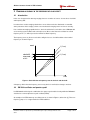
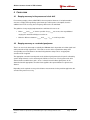
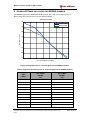
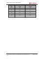
APPLICATION NOTE: APS011
APS011 APPLICATION NOTE
SOURCES OF ERROR IN
DW1000 BASED TWO-WAY
RANGING (TWR) SCHEMES
Version 1.0
This document is subject to change without
notice
© DecaWave 2014 This document is confidential and contains information which is proprietary to
DecaWave Limited. No reproduction is permitted without prior express written permission of the
author
APS011: Sources of error in TWR schemes
TABLE OF CONTENTS
1
INTRODUCTION ........................................................................................................................................4
1.1
1.2
2
RANGING ACCURACY IN THE PRESENCE OF CLOCK DRIFT .........................................................................5
2.1
2.2
2.3
2.4
2.5
3
OVERVIEW ................................................................................................................................................. 4
ABOUT THIS DOCUMENT................................................................................................................................ 4
INTRODUCTION ........................................................................................................................................... 5
DW1000 OSCILLATOR AND QUARTZ CRYSTAL.................................................................................................... 5
TWO-WAY RANGING (TWR) WITH CLOCK DRIFT................................................................................................. 6
SYMMETRIC DOUBLE-SIDED TWO-WAY RANGING (SDS-TWR) WITH CLOCK DRIFT..................................................... 8
SYMMETRIC DOUBLE-SIDED TWO-WAY RANGING (SDS-TWR) WITH FREQUENCY DRIFT ............................................. 9
RANGING ACCURACY VS RECEIVED SIGNAL LEVEL .................................................................................. 10
3.1
INTRODUCTION ......................................................................................................................................... 10
3.2
DECARANGING IMPLEMENTATION................................................................................................................. 10
3.3
DESIGN SPECIFIC DETAILS ............................................................................................................................ 11
3.4
FRIIS' PATH LOSS FORMULA AND RANGE BIAS CORRECTION VALUE ........................................................................ 11
3.4.1
Example Calculation...................................................................................................................... 14
4
CONCLUSION .......................................................................................................................................... 15
4.1
4.2
5
RANGING ACCURACY IN THE PRESENCE OF CLOCK DRIFT ..................................................................................... 15
RANGING ACCURACY VS. RECEIVED SIGNAL POWER ........................................................................................... 15
REFERENCES ........................................................................................................................................... 16
5.1
LISTING .................................................................................................................................................... 16
6
ABOUT DECAWAVE ................................................................................................................................ 17
7
APPENDIX A: DERIVING THE ERROR IN RANGING ACCURACY DUE TO DRIFT .......................................... 18
7.1
7.2
7.3
8
TWR WITH CLOCK DRIFT ............................................................................................................................. 18
SDS-TWR WITH CLOCK DRIFT ...................................................................................................................... 18
SDS-TWR WITH FREQUENCY DRIFT............................................................................................................... 19
APPENDIX B: RANGE BIAS FIGURES FOR 900 MHZ CHANNELS ................................................................ 20
LIST OF TABLES
TABLE 1: SAMPLE RANGE BIAS CORRECTION TABLE FROM DECARANGING TWR SOFTWARE FOR CHANNEL 2 ................................ 11
TABLE 2: RELATIONSHIP BETWEEN RSL AND RANGE BIAS CORRECTION FACTOR ...................................................................... 13
TABLE 3: CALIBRATION DISTANCE FOR CHANNELS AND PRF................................................................................................ 13
TABLE 4: TABLE OF REFERENCES .................................................................................................................................. 16
TABLE 5: RANGE BIAS CORRECTION FACTORS VS. RECEIVED SIGNAL LEVEL FOR 900MHZ CHANNELS ........................................... 20
© DecaWave 2014 This document is confidential and contains information which is proprietary to
DecaWave Limited. No reproduction is permitted without prior express written permission of the
author
Page 2 of 21
APS011: Sources of error in TWR schemes
LIST OF FIGURES
FIGURE 1: CLOCK DRIFT DUE TO FREQUENCY ERROR IN DEVICE A AND DEVICE B........................................................................ 5
FIGURE 2: RTXO FREQUENCY CHANGE AT TURN-ON ........................................................................................................... 6
FIGURE 3: EVB1000 CRYSTAL OSCILLATOR START-UP IN THE FREQUENCY DOMAIN. .................................................................. 6
FIGURE 4: TWO-WAY RANGING SCHEME .......................................................................................................................... 7
FIGURE 5: RANGING ERROR IN TWR SCHEME.................................................................................................................... 7
FIGURE 6: SYMMETRIC TWO-WAY RANGING SCHEME .......................................................................................................... 8
FIGURE 7: RANGING ERROR IN SDS-TWR SCHEME ............................................................................................................ 8
FIGURE 8: FREQUENCY DRIFT IN DEVICE A DURING QUARTZ CRYSTAL WARM-UP ....................................................................... 9
FIGURE 9: RANGING ERROR OF SDS-TWR SCHEME WITH FREQUENCY DRIFT IN DEVICE A .......................................................... 9
FIGURE 10: DIAGRAM ILLUSTRATING THE EFFECT OF RANGE BIAS ON THE REPORTED DISTANCE .................................................. 10
FIGURE 11: RANGE BIAS ERROR FOR A GIVEN RECEIVED SIGNAL LEVEL................................................................................... 12
© DecaWave 2014 This document is confidential and contains information which is proprietary to
DecaWave Limited. No reproduction is permitted without prior express written permission of the
author
Page 3 of 21
APS011: Sources of error in TWR schemes
1 INTRODUCTION
1.1
Overview
DecaWave’s DW1000, a multi-channel transceiver based on Ultra Wideband radio communications,
allows very accurate time-stamping of messages as they leave from and arrive at the transceiver.
This allows the construction of a number of different system topologies in the area of real time
location systems and proximity measurement devices.
The simplest of such topologies is where two nodes communicate between themselves, exchange
messages and based on transmit and receive timestamps of those messages they can calculate the
round trip time of the signal between the two nodes and hence the time of flight and therefore the
distance between the two nodes.
A complete description of DecaWave’s two-way ranging protocol is described in other documents
available from DecaWave. This Application Note focuses on the sources of error in the reported
timestamps and what corrections / mitigation strategies the system designer can employ to report as
accurate a result as possible.
1.2
About this document
This document deals with two fundamental sources of error: •
•
Errors related to clock drift in the two nodes
Errors related to incident signal level at a node
These are dealt with in individual sections.
Other application notes are available from DecaWave and you should contact your local
representative or [email protected] for more information.
© DecaWave 2014 This document is confidential and contains information which is proprietary to
DecaWave Limited. No reproduction is permitted without prior express written permission of the
author
Page 4 of 21
APS011: Sources of error in TWR schemes
2 RANGING ACCURACY IN THE PRESENCE OF CLOCK DRIFT
2.1
Introduction
In the case of tag-to-anchor two-way ranging, there are a number of sources of error due to clock drift
and frequency drift.
In order to have a robust ranging solution these errors either need to be eliminated or controlled.
Some parameters in the ranging scheme can exacerbate the ranging error if not chosen correctly.
If we consider two ranging capable devices, device A and device B, each device has a DW1000 with
a free running crystal oscillator and a microprocessor. We assume that each oscillator has a fixed
frequency error , with respect to the nominal oscillator frequency.
The frequency errors or offset on each device will give rise to a clock drift relative to the nominal
frequency as shown in Figure 1.
count
f.(1+eA)
f
clock drift A
measured
B
at t=t 1
f.(1+eB)
t0
t1
time
Figure 1: Clock drift due to frequency error in device A and device B
A frequency drift is when the frequency error on any device is not fixed, but changes over time.
2.2
DW1000 oscillator and quartz crystal
In a DW1000 based design the combination of a quartz crystal and the circuitry within the DW1000 is
classified as a room temperature crystal oscillator (RTXO).
An example of an RTXO warm-up at oscillator turn-on is shown in Figure 2, taken from [3]. There are
frequency jumps of +/- 0.5 ppm before the RTXO stabilizes.
© DecaWave 2014 This document is confidential and contains information which is proprietary to
DecaWave Limited. No reproduction is permitted without prior express written permission of the
author
Page 5 of 21
APS011: Sources of error in TWR schemes
+0.5
∆f/f (ppm)
-0.5
time (min)
Figure 2: RTXO frequency change at turn-on
DecaWave’s EVB1000 evaluation board, two of which are included in our EVK1000 evaluation kit,
uses such an RTXO. Measurements of the frequency of the crystal oscillator on the EVB1000 were
taken during crystal warm-up and are plotted in Figure 3. This shows a similar effect of frequency
jumps before it reaches stability.
0 .2
0 .1
∆f/f (ppm)
-0 .1
0
-0 .2
0
200
400
600
800
1000
1200
1400
time (ms)
Figure 3: EVB1000 crystal oscillator start-up in the frequency domain.
2.3
Two-way ranging (TWR) with clock drift
Consider the ranging scheme shown in Figure 4; the start of the ranging transaction begins by device
A sending a message to device B. Now device B waits a known amount of time and sends a response
back to device A.
© DecaWave 2014 This document is confidential and contains information which is proprietary to
DecaWave Limited. No reproduction is permitted without prior express written permission of the
author
Page 6 of 21
APS011: Sources of error in TWR schemes
device A
device B
350
treplyB = 10 us
treplyB = 100 us
treplyB = 1000 us
300
TOF
treplyB
TOF
Ranging error (cm)
250
troundA
200
150
100
50
0
0
5
10
15
20
eA-eB (ppm)
time
time
Figure 4: Two-way ranging scheme
Figure 5: Ranging error in TWR scheme
The dominant error in the ranging accuracy of this scheme is given by,
1
= ( − )
2
We can see that there is a strong dependence on in this equation. A plot of this error is shown
in Figure 5.
For practical values of and frequency offset, the error in the accuracy of the range is large.
© DecaWave 2014 This document is confidential and contains information which is proprietary to
DecaWave Limited. No reproduction is permitted without prior express written permission of the
author
Page 7 of 21
APS011: Sources of error in TWR schemes
2.4
Symmetric double-sided two-way ranging (SDS-TWR) with clock drift
The error in ranging accuracy in the simple two-way ranging scheme is large even with small
frequency offsets. An alternative scheme to minimize the error by introducing another message in the
ranging transaction is shown in Figure 6.
device A
device B
16
∆reply = 1 us
∆reply = 10 us
∆reply = 100 us
14
TOF
troundA
treplyB
TOF
TOF
Ranging error (cm)
12
10
8
6
4
treplyA
troundB
2
0
0
TOF
5
10
15
20
eA-eB (ppm)
time
time
Figure 6: Symmetric two-way ranging
scheme
Figure 7: Ranging error in SDS-TWR scheme
The dominant error in the ranging accuracy of this scheme is given by;
=
1
∆
( − )
4 Now we can see that the dependence on has been eliminated, the error is now dependent
upon ∆ , which is the difference between and . As a result, the error in the ranging
accuracy is much smaller as plotted in Figure 7.
© DecaWave 2014 This document is confidential and contains information which is proprietary to
DecaWave Limited. No reproduction is permitted without prior express written permission of the
author
Page 8 of 21
APS011: Sources of error in TWR schemes
2.5
Symmetric double-sided two-way ranging (SDS-TWR) with frequency drift
For lowest power operation, battery powered devices remain in the SLEEP mode with the crystal
oscillator off, so to perform a ranging transaction, the device is switched on, the transaction is
completed and the device is switched off again.
In this case the ranging transaction is performed while one of the devices is transitioning through the
crystal warm-up phase. This means there is a frequency drift on one of the devices during the ranging
transaction. The frequency error on device B remains constant.
We assume that the cumulative error of the frequency drift on device A can be approximated as two
separate frequency errors, , as shown in Figure 8.
16
count
f.(1+eAD )
treply = 1 ms
treply = 10 ms
treply = 100 ms
14
f
f.(1+eA)
Ranging error (cm)
12
f.(1+eB)
10
8
6
4
2
frequency drift
0
0
t0
time
Figure 8: Frequency drift in device A during
quartz crystal warm-up
0.005
0.01
0.015
0.02
eA-eAD (ppm)
Figure 9: Ranging error of SDS-TWR scheme
with frequency drift in device A
The dominant error in the ranging accuracy with frequency drift is now given by: 1
= ( − )
4
Now due to the frequency drift, the error in the ranging accuracy is dependent upon , this error
is plotted in Figure 9.
The deceptive problem with this ranging error is that it will be slightly different on each oscillator startup and from crystal to crystal. In essence this can be considered as a random frequency offset,
therefore its effect needs to be minimized.
© DecaWave 2014 This document is confidential and contains information which is proprietary to
DecaWave Limited. No reproduction is permitted without prior express written permission of the
author
Page 9 of 21
APS011: Sources of error in TWR schemes
3 RANGING ACCURACY VS RECEIVED SIGNAL LEVEL
3.1
Introduction
Ideally there should be no relationship between the reported timestamp of a received signal and the
received signal level. In practice a bias which varies with received signal level (RSL) can be observed
in the reported time-stamp compared with the correct value and this leads to a bias in the calculated
time of flight based on those time-stamps. This is illustrated in Figure 10 below where the red line,
labelled “Ideal” indicates the ideal result (constant) and the blue line, labelled “Actual” indicates the
actual measured result (which varies with received signal level).
500 MHz Bandwidth
reported distance
-5
0
Actual
-5
Ideal
-95
-90
-85
-80
Range Bias Effect (cm)
-10
-10
-75
-70
-65
-60
-55
-50
Received Signal Level (dBm)
Figure 10: Diagram illustrating the effect of range bias on the reported distance
For most applications this bias can be ignored, however higher precision ranging applications must
correct for this effect. This can be achieved in software by applying a correction factor.
3.2
DecaRanging Implementation
DecaRanging ARM-based source code, which includes DW1000 driver code, includes range bias
adjustment software to allow for this effect. This allows DecaWave's EVK1000 two way ranging
demonstration kit to achieve its target accuracy.
The DecaRanging ARM based source code takes a simple approach to compensating for this range
bias effect. The reported range from the TWR operation is used as an index to a table of range
© DecaWave 2014 This document is confidential and contains information which is proprietary to
DecaWave Limited. No reproduction is permitted without prior express written permission of the
author
Page 10 of 21
APS011: Sources of error in TWR schemes
adjustment figures which are used to adjust the reported range to allow for the effect. This adjusted
figure is then reported as the result of the TWR operation. Table 1 gives a sample of such a table
where the measured TWR distance is related to the correction factor for a given PRF. These tables
can be investigated in the DecaRanging source code.
Table 1: Sample range bias correction table from DecaRanging TWR software for channel 2
Measured TWR distance
(m)
3.3
Range Bias Correction Factor Applied
For channel 2 (cm)
PRF 16 MHz
PRF 64 MHz
1.00
-21
-13
1.25
-20
-11
1.50
-19
-11
1.75
-19
-10
2.00
-18
-10
Design Specific Details
The description of the EVK1000’s DecaRanging software above presents a simplified example of
compensating for this range bias effect. This explanation describes getting the measured distance of
the system and applying a correction factor to correct for the range bias effect, which is dependent on
the measured distance.
However, the effect of range bias is actually dependant on received signal level (RSL) at the pins of
the chip. This is affected by antenna gain, transmitted power and any other sources of loss or gain in
the system. The EVK1000 has a transmit power of -41.3 dBm/MHz and a 0dB antenna gain.
Should your system transmit at a different power level, use a low noise amplifier (LNA) or have other
sources of power gain or loss in the system then the correction factor you need to apply will be
different. A more in-depth understanding will be required in this scenario
The RSL can be calculated using the formula described in the next section and this can be used in a
table relating RSL to range bias figure, also presented in the next section, to determine what range
bias correction factor you need to apply.
3.4
Friis' path loss formula and range bias correction value
In the case of a line-of-sight channel, the signal power of the unobstructed first path as it arrives at the
receiver can be calculated based on the distance reported by the chip using Friis' path loss formula:
PR [dBm] = PT [dBm] + G[dB] + 20 log10(c)-20 log10(4πfcR)
Where: •
•
PR is the received signal level;
PT is the transmitted power. In a properly calibrated system, the DW1000 transmits
-41.3 dBm / MHz into a 500 MHz bandwidth channel, corresponding to a total power PT of 14.3 dBm;
© DecaWave 2014 This document is confidential and contains information which is proprietary to
DecaWave Limited. No reproduction is permitted without prior express written permission of the
author
Page 11 of 21
APS011: Sources of error in TWR schemes
•
•
•
•
G includes the antenna gains of the transmitting and receiving antennas, as well as any other
gain from external amplifiers and / or PCB losses;
c is the speed of light, 299792458 m/s;
fc is the centre frequency of the channel used, expressed in Hertz;
R is the reported distance in meters returned from the TWR operation.
Knowing your system parameters such as antenna gain G, PT etc. it is possible to calculate PR
the received signal level (RSL). Using this RSL in
Table 2 the range bias correction can be determined.
The reported distance can then be corrected such that: Actual distance = Reported distance - Range Bias Correction
Where: Actual distance
=
the physical distance being measured
Reported distance
=
the distance reported by the un-corrected TWR operation
Range Bias Correction =
the adjustment figure in cm taken from Table 2
500 MHz Bandwidth
15
16 MHz PRF
64 MHz PRF
10
5
Range Bias (cm)
0
-5
-10
-15
-20
-95
-90
-85
-80
-75
-70
Received Signal Level (dBm)
-65
-60
Figure 11: Range bias error for a given received signal level
© DecaWave 2014 This document is confidential and contains information which is proprietary to
DecaWave Limited. No reproduction is permitted without prior express written permission of the
author
Page 12 of 21
APS011: Sources of error in TWR schemes
Table 2: Relationship between RSL and range bias correction factor
PRF 16 MHz
PRF 64 MHz
500 MHz
500 MHz
(cm)
(cm)
-61
-19.8
-11.0
-63
-18.7
-10.5
-65
-17.9
-10.0
-67
-16.3
-9.3
-69
-14.3
-8.2
-71
-12.7
-6.9
-73
-10.9
-5.1
-75
-8.4
-2.7
-77
-5.9
0.0
-79
-3.1
2.1
-81
0.0
3.5
-83
3.6
4.2
-85
6.5
4.9
-87
8.4
6.2
RSL
(dBm)
-89
9.7
7.1
-91
10.6
7.6
-93
11.0
8.1
Figure 11 and Table 2 use an antenna delay calibration (see [2] for an explanation of this) that places
the zero point of the range bias (i.e. where the actual and ideal curves in Figure 10 intersect) at -81
dBm for a PRF of 16 MHz and -77 dBm for a PRF of 64 MHz. In this way, the zero point is towards
the middle of the range bias variation. This is to ensure we have the minimum error for applications
that do not correct for range bias. You may choose to calibrate the antenna delay such that the zero
point of the range bias moves towards higher or lower signal levels depending on your application and
whether you need accuracy at very short ranges or not.
Table 3 below lists the corresponding calibration distances used for the different channels and
different PRFs.
Table 3: Calibration distance for channels and PRF
Channel Number
fc (MHz)
Bandwidth
(MHz)
PRF (MHz)
Calibration Distance
(m)
2
3993.6
499.2
16
12.9
2
3993.6
499.2
64
8.1
3
4492.8
499.2
16
11.5
3
4492.8
499.2
64
7.2
4
3993.6
900
16 / 64
8.7
5
6489.6
499.2
16
7.9
© DecaWave 2014 This document is confidential and contains information which is proprietary to
DecaWave Limited. No reproduction is permitted without prior express written permission of the
author
Page 13 of 21
APS011: Sources of error in TWR schemes
Channel Number
fc (MHz)
Bandwidth
(MHz)
5
6489.6
499.2
64
5.0
7
6489.6
499.2
16 / 64
5.3
PRF (MHz)
Calibration Distance
(m)
Also included in Appendix B is the corresponding figure and table for the two 900 MHz channels
included in the DW1000.
3.4.1
Example Calculation
For a system with the following parameters
G = +1 dB; in the TWR case we must allow for two antenna gains, so +2 dB.
PT = -14.3 dBm
R=2m
6
fc = 3993.6 x 10 for channel number 2, see Table 3.
and using this formula: PR [dBm] = PT [dBm] + G[dB] + 20 log10(c) - 20 log10(4πfcR)
we find that: 6
PR = -14.3 + 2 +20 log10(299792458) - 20 log10(4 x 3.1415926 x 3993.6 x10 x 2)
PR = -14.3 + 2 + 169.536 - 220.032
PR = -62.8 dBm
Using this result in Table 2 (rounding up to -63 dBm) gives a correction of -18.7 cm for this
measurement.
© DecaWave 2014 This document is confidential and contains information which is proprietary to
DecaWave Limited. No reproduction is permitted without prior express written permission of the
author
Page 14 of 21
APS011: Sources of error in TWR schemes
4 CONCLUSION
4.1
Ranging accuracy in the presence of clock drift
For a two-way ranging scheme, SDS-TWR is the most practical. However, if an implementation
executes a ranging exchange during crystal warm-up to reduce power consumption, then the
additional error in the accuracy due to frequency drift needs to be minimized.
The guidelines for any ranging implementation to minimize this error are to: -
4.2
•
Make and as short as possible. If say was 10 ms, then any additional
ranging error would be unlikely to exceed 2 cm.
•
Make the difference between and , ∆ as small as possible.
Ranging accuracy vs. received signal power
There is an error in the timestamp recorded by the DW1000 that is dependent on incident signal level
and in particular on high signal levels. This leads to an error in the reported time-stamp and a
corresponding error in the distance calculated using that time-stamps unless an appropriate
correction factor is applied.
The appropriate correction factor depends on the incident signal power at the chip and is affected by
system design elements such as antenna gain, PCB losses and so on. Each system needs to be
characterized to establish these gains / losses so that the actual incident signal power can be
determined and the appropriate correction factor applied to the reported distance to give the true
distance.
Depending on the required accuracy of the distance measurements for the particular application, this
correction may not be necessary.
© DecaWave 2014 This document is confidential and contains information which is proprietary to
DecaWave Limited. No reproduction is permitted without prior express written permission of the
author
Page 15 of 21
APS011: Sources of error in TWR schemes
5 REFERENCES
5.1
Listing
Reference is made to the following documents in the course of this Application Note: Table 4: Table of References
Ref
Author
Date
Version
Title
[1]
DecaWave
Current
DW1000 Data Sheet
[2]
DecaWave
Current
DW1000 User Manual
[3]
Hewlett
Packard
Current
Fundamentals of Quartz Oscillators, Application
Note AN200-2
© DecaWave 2014 This document is confidential and contains information which is proprietary to
DecaWave Limited. No reproduction is permitted without prior express written permission of the
author
Page 16 of 21
APS011: Sources of error in TWR schemes
6 ABOUT DECAWAVE
DecaWave is a pioneering fabless semiconductor company whose flagship product, the DW1000, is a
complete, single chip CMOS Ultra-Wideband IC based on the IEEE 802.15.4-2011 UWB standard.
This device is the first in a family of parts that will operate at data rates of 110 kbps, 850 kbps and
6.8 Mbps.
The resulting silicon has a wide range of standards-based applications for both Real Time Location
Systems (RTLS) and Ultra Low Power Wireless Transceivers in areas as diverse as manufacturing,
healthcare, lighting, security, transport, inventory & supply chain management.
Further Information
For further information on this or any other DecaWave product contact a sales representative as
follows: DecaWave Ltd
Adelaide Chambers
Peter Street
Dublin 8
t: +353 1 6975030
e: [email protected]
w: www.decawave.com
© DecaWave 2014 This document is confidential and contains information which is proprietary to
DecaWave Limited. No reproduction is permitted without prior express written permission of the
author
Page 17 of 21
APS011: Sources of error in TWR schemes
7 APPENDIX A: DERIVING THE ERROR IN RANGING ACCURACY DUE TO DRIFT
7.1
TWR with clock drift
With the final response message device A can measure the round trip time of the transaction as
follows: = 2 + And extract the time of flight (TOF): 2 = − Because of the clock drift, device A actually measures an estimated TOF which is given by: 2 = (1 + ) − (1 + )
The difference between the true TOF and the estimated TOF gives the error in the ranging
transaction: 2 − 2 = (1 + ) − (1 + ) − ( − )
Substituting for yields the final error: (
" #$ − !#$ = !#$. &' + *+&,-./ (&' − &/ )
!
)
7.2
SDS-TWR with clock drift
Now each device measures a round trip time as follows: = 2 + = 2 + We can extract the TOF by combining these two round trip times as follows: 4 = − + − As before due to clock drift, device A and device B measure estimated round trip times, so the
estimated TOF is given by: 4 = ( − )(1 + ) + ( − )(1 + )
The difference between the estimated TOF and the true TOF gives the error in the ranging transaction
as: 4 − 4 = ( − )(1 + ) + ( − )(1 + ) − ( − + − )
4 − 4 = ( − ) + ( − )
© DecaWave 2014 This document is confidential and contains information which is proprietary to
DecaWave Limited. No reproduction is permitted without prior express written permission of the
author
Page 18 of 21
APS011: Sources of error in TWR schemes
If we assume that = and = + ∆ then: = 2 + + ∆
= 2 + So the error becomes: 4 − 4 = (2 + + ∆ − ) + (2 + − − ∆ )
Which reduces to: " #$ − !#$ =
!
7.3
(
(
!#$(&' + &/ ) + ∆+&,-. (&' − &/ )
)
0
SDS-TWR with frequency drift
The true TOF is the same as for the SDS-TWR scheme: 4 = − + − However, now we have frequency drift in device A, represented by and , so the estimated TOF,
based on the round trip time measurements, becomes: 4 = ( )(1 + ) − (1 + ) + ( − )(1 + )
Again, the difference between the true TOF and estimated TOF gives the error for the ranging
transaction: 4 − 4 = ( )(1 + ) − (1 + ) + 1 − 2(1 + ) − ( −
+ − )
4 − 4 = ( ) − ( ) + 1 − 2( )
If we assume that = and = + ∆ then: = 2 + + ∆
= 2 + Then the error becomes: 4 − 4 = 12 + + ∆ 2( ) − ( ) + 12 + − − ∆ 2( )
Which reduces to: " #$ − !#$ = ( !#$(&' + &/ ) + ( ∆+&,-. (&' − &/ ) + ( *+&,-. (&' − &'3 )
!
)
0
0
© DecaWave 2014 This document is confidential and contains information which is proprietary to
DecaWave Limited. No reproduction is permitted without prior express written permission of the
author
Page 19 of 21
APS011: Sources of error in TWR schemes
8 APPENDIX B: RANGE BIAS FIGURES FOR 900 MHZ CHANNELS
The DW1000 supports two 900 MHz bandwidth channels (Ch 4 & 6). These channels have a
different range bias characteristic due to their wider bandwidth.
900 MHz Bandwidth
40
PRF 16 MHz
PRF 64 MHz
30
Range Bias (cm)
20
10
0
-10
-20
-30
-95
-90
-85
-80
-75
-70
Received Signal Level (dBm)
-65
-60
Figure 17: Range bias error vs. received signal level for 900MHz channels.
Table 5: Range bias correction factors vs. received signal level for 900MHz channels
PRF 16 MHz
PRF 64 MHz
900 MHz
900 MHz
(cm)
(cm)
-61
-27.5
-29.5
-63
-24.4
-26.6
-65
-21.0
-23.5
-67
-17.6
-19.9
-69
-13.8
-15.0
-71
-9.5
-10.0
-73
-5.1
-5.8
-75
0.0
0.0
-77
4.2
4.9
-79
9.7
9.1
-81
15.8
12.7
RSL
(dBm)
© DecaWave 2014 This document is confidential and contains information which is proprietary to
DecaWave Limited. No reproduction is permitted without prior express written permission of the
author
Page 20 of 21
APS011: Sources of error in TWR schemes
PRF 16 MHz
PRF 64 MHz
900 MHz
900 MHz
(cm)
(cm)
-83
21.0
15.3
-85
25.4
17.5
-87
29.4
19.7
-89
32.1
23.3
-91
33.9
24.5
-93
35.6
26.4
-95
39.4
28.4
RSL
(dBm)
© DecaWave 2014 This document is confidential and contains information which is proprietary to
DecaWave Limited. No reproduction is permitted without prior express written permission of the
author
Page 21 of 21