1
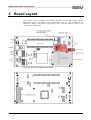
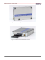
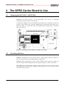
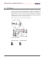
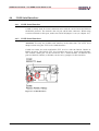
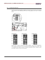
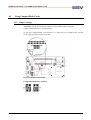
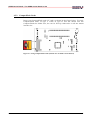
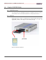
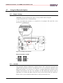
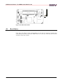
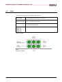
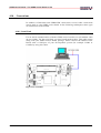
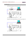
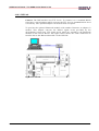
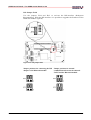
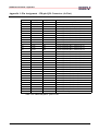
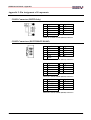
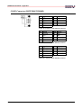
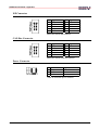
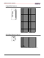
GPRS Carrier Board – Documentation
GPRS Carrier Board CAB/GPRS1
User Manual
GPRS Carrier Board – Content
Content
1
INTRODUCTION ...........................................................................................................................3
1.1
1.2
1.3
Conventions Used in this Document ..........................................................................................3
Checklist.....................................................................................................................................4
Main Features .............................................................................................................................5
2
BOARD LAYOUT...........................................................................................................................6
3
BOARD COMPONENTS ...............................................................................................................8
3.1
3.2
3.3
3.4
3.5
3.6
3.7
3.8
3.9
3.10
3.11
4
THE GPRS CARRIER BOARD IN USE....................................................................................11
4.1
4.2
4.3
4.4
4.5
4.6
4.7
4.8
4.9
4.10
5
128-pin QIL socket.....................................................................................................................8
GSM/GPRS Modem...................................................................................................................8
Bluetooth Option ........................................................................................................................8
CompactFlash Interface..............................................................................................................9
10/100Mbps Ethernet .................................................................................................................9
CAN-Bus Option........................................................................................................................9
COM Serial Interfaces................................................................................................................9
Onboard Jumper .........................................................................................................................9
LEDs.........................................................................................................................................10
Reset Button .............................................................................................................................10
Power Connector ......................................................................................................................10
Mounting the DIL/NetPC (ADNP/1520) .................................................................................11
Providing with Power...............................................................................................................11
RCM Jumper ............................................................................................................................12
COM Serial Interfaces..............................................................................................................13
Using CompactFlash Cards ......................................................................................................16
Using the GSM/GPRS Modem ................................................................................................18
Using the Bluetooth Option......................................................................................................19
Reset Button .............................................................................................................................20
LEDs.........................................................................................................................................21
Connections ..............................................................................................................................22
APPENDIX ....................................................................................................................................26
SSV EMBEDDED SYSTEMS
2
GPRS Carrier Board – Introduction
1 Introduction
The GPRS Carrier Board is an universal carrier board for industrial applications
such like process automation, remote support and services. The central element is
a modular computer of the DIL/NetPC series. The board offers possibilities to use
a GPRS modem as well as an optional module for Bluetooth ® wireless technology
or a CompactFlash™ interface.
This document describes how to start with the GPRS Carrier Board. For further
information about the individual components of this product you may follow the
links from our website at: http://www.dilnetpc.com
Our Website contains a lot of technical information, which will be updated in
regular periods.
1.1
Conventions Used in this Document
Convention
Usage
italic
Filenames, as well as Internet addresses such as www.ssvembedded.de
italic
User inputs, command lines and pathnames
bold
New terms
monospace text
Program code
Table 1-1: Convention usage
SSV EMBEDDED SYSTEMS
3
GPRS Carrier Board – Introduction
1.2
Checklist
Compare the content of your GPRS Carrier Board package with the standard
checklist below. If any item is missing or appears to be damaged, please contact
SSV Embedded Systems.
Standard Items
•
GPRS Carrier Board
•
DIL/NetPC ADNP/1520
•
Null modem cable
•
Power supply
•
Power cable
•
User manual
•
Support CD-ROM
Optional Items
•
ISP adapter (Bluetooth option only)
Please note that SSV does not include a Bluetooth or GSM/GPRS antenna.
SSV EMBEDDED SYSTEMS
4
GPRS Carrier Board – Introduction
1.3
Main Features
GPRS Carrier Board
•
128-pin QIL socket for one DIL/NetPC (like the ADNP/1520)
•
10/100Base-T Ethernet Interface
•
RS232 Serial interface (COM1)
•
RS232/422/485 Serial interfaces (COM2 and COM3)
•
In-System Programming interface (Bluetooth option only)
•
HF-Out interface to connect an external antenna (Bluetooth option
only)
•
Dual Band GSM/GPRS modem E-GSM 900/1800
•
RF connector type MMCX (Miniature Micro Connector) to connect an
external GSM/GPRS antenna
•
CAN-bus interface (only with DNP/5280)
•
CompactFlash card interface
•
6 LEDs
•
1 Reset switch
•
5VDC Power Input Connector
•
Size 180 x 100 mm
DIL/NetPC ADNP/1520 (standard)
•
AMD™ SC520 CPU with 133 MHz Clock Speed and FPU
•
32/64 MByte SDRAM Memory
•
16 MByte Flash Memory
•
10/100Mbps Ethernet Interface
•
Real Time Clock
•
IDE Support
•
Two 16C550 UART Serial Ports
•
20-bit General Purpose High-Speed Parallel I/O
•
7 Interrupt Inputs, 4 Chip Select Outputs
•
In-System Programming Features
•
128-pin QIL connector
•
3.3 Volt Low Power Design, Single 3.3 VDC Supply
•
Size 82 x 36 mm
SSV EMBEDDED SYSTEMS
5
GPRS Carrier Board – Board Layout
2 Board Layout
The design of your GPRS Carrier Board depends on the DIL/NetPC and the
Bluetooth option. Therefore some components like the ISP connector, the
Bluetooth chipset, the antenna connector, or the CAN-bus interface may not be
mounted on your board.
Figure 2-1: Top view of GPRS Carrier Board
Figure 2-2: Bottom view of GPRS Carrier Board
SSV EMBEDDED SYSTEMS
6
GPRS Carrier Board – Board Layout
Figure 2-3: Wavecom® Integra® GSM/GPRS modem
Figure 2-4: SIM card slot and MMCX antenna connector
SSV EMBEDDED SYSTEMS
7
GPRS Carrier Board – Board Components
3 Board Components
3.1
128-pin QIL socket
The QIL socket with 128 pins can hold one DIL/NetPC like the ADNP/1520.
Please refer to chapter 4.1 how to mount your DIL/NetPC safely. If you are
interested in pin signals please refer to the appendix.
3.2
GSM/GPRS Modem
The board contains a GSM/GPRS modem made by Wavecom®. Some basic
features are:
3.3
•
Dual Band integrated GSM modem (EGSM900/1800 MHz)
•
Fully Type Approved
•
Compliant with ETSI GSM Phase 2+ standard (Normal MS)
•
Class 4 (2W at 900 MHz)
•
Class 1 (1W at 1800 MHz)
•
MMCX antenna connector for 900 and 1800 MHz
•
Internal 3V SIM reader (5V SIM with external level shifter)
Bluetooth Option
The Bluetooth technology is a standard for short-range wireless communications
between different devices. The module option on the carrier board is a complete
baseband/RF solution that allows you a quick and easy integration of Bluetooth
wireless technology outgoing from Handheld, PDA, Cell Phone or Laptop into
embedded or standard devices. The Bluetooth option follows the Bluetooth
standard with all its included advantages like transmission security and noise
immunity in the industrial environment area.
The onboard Bluetooth module allows the connection between the ADNP/1520
and other devices via Bluetooth. To use all features offered by the Bluetooth
module it is necessary to connect a standard Bluetooth antenna to the GPRS
Carrier Board. For this, any standard 2.4 GHz Bluetooth antenna with an
impedance of 50 ohm and SMA connector can be used with the HF-out connector.
The GPRS Carrier Board offers an ISP interface. This interface is used to
communicate with the onboard Bluetooth module, e.g. to load a new firmware.
SSV EMBEDDED SYSTEMS
8
GPRS Carrier Board – Board Components
3.4
CompactFlash Interface
On the back side of the GPRS Carrier Board a CompactFlash interface is located,
that will operate with 3.3V.
3.5
10/100Mbps Ethernet
The ADNP/1520 is using an SMSC™ LAN91C111 chip that allows Ethernet
connectivity with a speed up to 100Mbps. The RJ45 Ethernet interface on the
GPRS Carrier Board is just a simple connection over a transformer to the 128 QIL
interface pins, which are connected to the SMSC LAN controller on the
ADNP/1520.
3.6
CAN-Bus Option
The GPRS carrier board offers a CAN-bus option. The CAN-bus interface will be
available if using the DIL/NetPC DNP/5280.
3.7
COM Serial Interfaces
The GPRS Carrier Board is equipped with 3 serial COM interfaces: COM1 (9-pin
sub-D male connector), COM2 (10-pin boxed header), and COM3 (9-pin sub-D
male connector).
COM1 is used for initial communication with the carrier board. It follows the
RS232 protocol.
COM2 can either be used with RS232 TTL level or with the RS232, RS485 or
RS422 protocol.
COM3 can be used with the RS232, RS485 or RS 422 protocol.
3.8
Onboard Jumper
JP1:
JP2/3:
JP4 - JP8
JP9 - JP13
JP14/15
SSV EMBEDDED SYSTEMS
RCM jumper for terminal mode
Chip select (CS) jumper
Jumper field for setting COM2 to RS232/RS485/RS422
Jumper field for setting COM3 to RS232/RS485/RS422
Jumpers for using the ISP interface (Bluetooth option only)
9
GPRS Carrier Board – Board Components
3.9
LEDs
You will find 6 LEDs on your GPRS Carrier Board, which are illustrated in figure
3-1.
Figure 3-1: LEDs
3.10
Reset Button
Press the reset button if the system hangs or you need to restart it. Pressing the
reset button will only restart the ADNP/1520. To reset connected devices, turn off
power from the system.
3.11
Power Connector
Caution: Providing the GPRS Carrier Board with a voltage higher than the
regular 5V DC ±10% could resolve in damaged board components.
The GPRS Carrier Board needs a supply voltage of 5V DC to work. In your
carrier board package you will find a plug-in power supply unit to provide the
system with the necessary power.
SSV EMBEDDED SYSTEMS
10
GPRS Carrier Board – The GPRS Carrier Board in Use
4 The GPRS Carrier Board in Use
4.1
Mounting the DIL/NetPC (ADNP/1520)
Caution: Too high pressure on the DIL/NetPC can resolve in damaged
components and/or in bent or broken pins.
To mount the ADNP/1520 on the GPRS Carrier Board set it carefully on the 128pin QIL socket. Please note, that the ADNP/1520 is positioned in the right way as
shown in figure 4-1. After that, press the ADNP/1520 carefully down, so that the
QIL socket fixes it.
Figure 4-1: Mounting the ADNP/1520 on the GPRS Carrier Board
4.2
Providing with Power
Caution: Providing the Carrier Board with a voltage higher than the regular 5V
DC ±10% could resolve in damaged board components.
Caution: SSV recommends to power off the GPRS carrier board every time you
alter or modify board configurations like jumper settings or cable connections.
The GPRS Carrier Board needs a supply voltage of 5VDC to work. In your carrier
board package you will find a plug-in power supply unit to provide the system
with the necessary power.
SSV EMBEDDED SYSTEMS
11
GPRS Carrier Board – The GPRS Carrier Board in Use
4.3
RCM Jumper
Use this jumper to activate the RCM mode of the ADNP/1520. The RCM mode
(Remote Console Mode) offers the possibility to control the ADNP/1520 via
terminal program. To activate the RCM mode place a jumper cap on both pins of
the RCM jumper, so that it is short. If you remove the jumper cap, or place the
jumper cap on just one pin, the jumper is open and you can not use the RCM
mode.When closed you will see some boot messages on the serial port COM1. If
the RCM jumper is open, these messages are blocked.
Figure 4-2 shows the exact position of the RCM jumper.
Figure 4-2: RCM jumper
RCM mode enabled
SSV EMBEDDED SYSTEMS
RCM mode disabled
12
GPRS Carrier Board – The GPRS Carrier Board in Use
4.4
COM Serial Interfaces
4.4.1 COM1 Serial Interface
COM1 is mostly used for initial communication with the carrier board and follows
the RS232 protocol. The interface has a 9-pin sub-D male connector. When using
a remote terminal on this port, make sure the RCM jumper is set (see chapter 4.3).
4.4.2 COM2 Serial Interfaces
Attention: Use only one COM2 serial interface at the same time. Use a TTL level
adapter when using the TTL level COM2 interface.
COM2 can either be used with RS232 TTL level or with the RS232, RS485 or
RS422 protocol. The RS232 TTL level interface has got a 10-pin boxed header.
The second COM2 port on the board has also a boxed header. In addition the
protocol (RS232, RS485, or RS422) can be set by jumpers for this interface.
Figure 4-3: COM2 interfaces
SSV EMBEDDED SYSTEMS
13
GPRS Carrier Board – The GPRS Carrier Board in Use
With jumpers JP4 to JP8 the COM2 protocol can be set as shown in figure 4-4.
Figure 4-4: COM2 jumper field
COM2 RS232
COM2 RS485
COM2 RS422
Jumper JP8 is used as termination jumper (default = off). To use termination,
three optional resistors have to be onboard. Set the JP8 jumper cap on pins 1 and 2
to terminate the COM2 interface for RS485 and RS422 mode. In RS232 mode the
COM2 interface can not be terminated.
SSV EMBEDDED SYSTEMS
14
GPRS Carrier Board – The GPRS Carrier Board in Use
4.4.3 COM3 Serial Interface
COM3 can be used with RS232, RS485 or RS 422 protocol. It has a 9-pin sub-D
male connector. The COM3 protocols can be set by jumpers JP9 to JP13 as shown
below.
Figure 4-5: COM3 jumper field
COM3 RS232
COM3 RS485
COM3 RS422
Jumper JP13 is used as termination jumper (default = off). To use termination,
three optional resistors have to be onboard. Set the JP13 jumper cap on pins 1 and
2 to terminate the COM3 interface for RS485 and RS422 mode. In RS232 mode
the COM3 interface can not be terminated.
SSV EMBEDDED SYSTEMS
15
GPRS Carrier Board – The GPRS Carrier Board in Use
4.5
Using CompactFlash Cards
4.5.1 Jumper Settings
Attention: Using the Bluetooth option is not possible when using the
CompactFlash interface simultaneously.
To use the CompactFlash card interface it is required to set jumpers JP2 and JP3
to the right positions as shown below.
Figure 4-6: Jumpers JP2 and JP3
CompactFlash interface enabled
SSV EMBEDDED SYSTEMS
16
GPRS Carrier Board – The GPRS Carrier Board in Use
4.5.2 CompactFlash Cards
Insert your CompactFlash card (CF card) as shown in the figure below. Use only
CompactFlash cards of type I. Cards of type II will not mount into the
CompactFlash slot. Make sure, the card is face-up. Otherwise it will not mount
into the slot.
Figure 4-7: Using CompactFlash cards (bottom view of GPRS Carrier Board)
SSV EMBEDDED SYSTEMS
17
GPRS Carrier Board – The GPRS Carrier Board in Use
4.6
Using the GSM/GPRS Modem
4.6.1 GSM/GPRS Antenna
The Integra Wavecom GSM/GPRS modem has an MMCX connector to hold an
antenna. Please refer to the antenna manual how to safely mount and use it.
4.6.2 SIM Card
Push in the pin lever with e.g. a ballpoint pen to open the SIM card slot of the
GSM/GPRS modem. Take out the card sledge and insert your SIM card
appropriately. Push the card sledge back into the modem softly.
Figure 4-8: Insertion of a SIM card
SSV EMBEDDED SYSTEMS
18
GPRS Carrier Board – The GPRS Carrier Board in Use
4.7
Using the Bluetooth Option
4.7.1 Jumper Settings
Attention: Using the Bluetooth option is not possible when using the
CompactFlash interface simultaneously.
To use the Bluetooth module it is required to set jumpers JP2 and JP3 to the
positions as shown below.
Figure 4-9: Jumpers JP2 and JP3
Bluetooth module enabled
4.7.2 Antenna
The optional onboard Bluetooth module allows the connection between the
ADNP/1520 and other devices via Bluetooth. To use all features offered by the
Bluetooth module it is necessary to connect a standard Bluetooth antenna to the
GPRS Carrier Board. For this, any standard 2.4 GHz Bluetooth antenna with an
impedance of 50 ohm and SMA connector can be used with the HF-out connector.
Please refer to your antenna manual how to safely mount and use it.
SSV EMBEDDED SYSTEMS
19
GPRS Carrier Board – The GPRS Carrier Board in Use
Figure 4-10: Bluetooth antenna
4.8
Reset Button
Press the reset button if the system hangs or you need to restart it. Pressing the
reset button will only restart the ADNP/1520. To reset any connected devices turn
off power from the system.
SSV EMBEDDED SYSTEMS
20
GPRS Carrier Board – The GPRS Carrier Board in Use
4.9
LEDs
Six LEDs are placed on your GPRS carrier board:
Power-LED
This LED lights when the board is powered.
The baseband activity LED flickers or lights up if there is some
Bluetooth
Baseband Activity traffic via the Bluetooth interface.
GPRS Flashing
The GPRS flashing LED flickers or lights up if there is some traffic
via the GPRS/GSM modem.
ADNP
PORT A/0
PORT A/1
PORT A/2
The function of these LEDs are user definable.
Table 4-1: LEDs
Figure 4-11: LEDs
SSV EMBEDDED SYSTEMS
21
GPRS Carrier Board – The GPRS Carrier Board in Use
4.10
Connections
In addition to Bluetooth and GPRS/GSM connections several cable connections
can be made to your GPRS carrier board. In the following subchapters three types
of connections are described.
4.10.1 Serial Link
For an initial communication with the GPRS carrier board use a null modem cable
on port COM1. For the serial link, you need a null modem cable. This cable comes
along with your GPRS Carrier Board package. Please connect the GPRS Carrier
Board with a COM port of your development system (for example COM1 or
COM2) by using this cable.
Figure 4-12: Serial link
SSV EMBEDDED SYSTEMS
22
GPRS Carrier Board – The GPRS Carrier Board in Use
4.10.2 Ethernet Link
The Ethernet link requires two standard 10 Base-T patch cables, one hub or switch
and an Ethernet LAN adapter for your development system.
Figure 4-13: Ethernet link with hub or switch
If you want to connect your development system directly to the GPRS Carrier
Board place a crossover cable between these two systems as shown in figure 4-14.
Figure 4-14: Ethernet link with crossover cable
SSV EMBEDDED SYSTEMS
23
GPRS Carrier Board – The GPRS Carrier Board in Use
4.10.3 ISP Link
Caution: The ISP interface uses TTL levels. To connect it to a standard RS232
serial port a special adapter which converts the TTL level to standard RS232 level
is necessary. This optional adapter can be delivered on request.
To provide the optional Bluetooth module with another firmware an adapter is
needed. This adapter converts the RS232 signal levels provided by the
development system into TTL signal levels which are needed by the Bluetooth
module on the Carrier Board. The figure below shows the cable connection to
transfer data to the Bluetooth module via the ISP link.
Figure 4-15: ISP link
SSV EMBEDDED SYSTEMS
24
GPRS Carrier Board – The GPRS Carrier Board in Use
ISP Jumper Field
Use the jumpers JP14 and JP15 to activate the ISP-interface (In-System
Programming). With the ISP interface it is possible to upgrade the firmware of the
Bluetooth module (option).
Figure 4-16: ISP jumper field
Jumper positions for connecting the ISP
adapter to the Bluetooth module
SSV EMBEDDED SYSTEMS
Jumper positions for normal
communication between the onboard
UART and the Bluetooth module
25
GPRS Carrier Board – Appendix
5 Appendix
The Appendices give you more detailed information about the signals on the
individual connectors. Table cells marked with NC indicate signals, which may be
not connected.
Appendix 1: Pin Assignment – 128-pin QIL Connector (1st Part)
Pin
1
2
3
4
5
6
7
8
9
10
11
12
13
14
15
16
17
18
19
20
21
22
23
24
25
26
27
28
29
30
31
32
Name
PA0
PA1
PA2
PA3
PA4
PA5
PA6
PA7
PB0
PB1
PB2
PB3
PB4
PB5
PB6
PB7
PC0
PC1
PC2
PC3
RXD1
TXD1
CTS1
RTS1
DCD1
DSR1
DTR1
RI1
RESIN
TX+
TXGND
Group
PIO
PIO
PIO
PIO
PIO
PIO
PIO
PIO
PIO
PIO
PIO
PIO
PIO
PIO
PIO
PIO
PIO
PIO
PIO
PIO
SIO
SIO
SIO
SIO
SIO
SIO
SIO
SIO
RESET
LAN
LAN
----
Function
Parallel I/O, Port A, Bit 0 *
Parallel I/O, Port A, Bit 1*
Parallel I/O, Port A, Bit 2*
Parallel I/O, Port A, Bit 3*
Parallel I/O, Port A, Bit 4*
Parallel I/O, Port A, Bit 5*
Parallel I/O, Port A, Bit 6*
Parallel I/O, Port A, Bit 7*
Parallel I/O, Port B, Bit 0*
Parallel I/O, Port B, Bit 1*
Parallel I/O, Port B, Bit 2*
Parallel I/O, Port B, Bit 3*
Parallel I/O, Port B, Bit 4*
Parallel I/O, Port B, Bit 5*
Parallel I/O, Port B, Bit 6*
Parallel I/O, Port B, Bit 7*
Parallel I/O, Port C, Bit 0*
Parallel I/O, Port C, Bit 1*
Parallel I/O, Port C, Bit 2*
Parallel I/O, Port C, Bit 3*
COM1 Serial Port, RXD Pin
COM1 Serial Port, TXD Pin
COM1 Serial Port, CTS Pin
COM1 Serial Port, RTS Pin
COM1 Serial Port, DCD Pin
COM1 Serial Port, DSR Pin
COM1 Serial Port, DTR Pin
COM1 Serial Port, RI Pin
Reset Input
Ethernet Interface, TX+ Pin
Ethernet Interface, TX- Pin
Ground
Table A1-1: ADNP/1520 pinout – pin 1 to 32
The PIO pins 1 to 20 are driven by an in-system programmable (ISP) high density
PLD (ispMACH256 or similar). It is possible to change the function of these pins
over the ADNP/1520 JTAG interface. Please contact our support staff for more
information.
SSV EMBEDDED SYSTEMS
26
GPRS Carrier Board – Appendix
Appendix 1: Pin Assignment – 128-pin QIL Connector (2nd Part)
Pin
33
34
35
36
37
38
39
40
41
42
43
44
45
46
47
48
49
50
51
52
53
54
55
56
57
58
59
60
61
62
63
64
Name
RX+
RXRESOUT
VBAT
CLKOUT
TXD2
RXD2
INT5
INT4
INT3
INT2
INT1
CS4
CS3
CS2
CS1
IOCHRDY
IOR
IOW
SA3
SA2
SA1
SA0
SD7
SD6
SD5
SD4
SD3
SD2
SD1
SD0
Vcc
Group
LAN
LAN
RESET
PSP
PSP
PSP
PSP
PSP
PSP
PSP
PSP
PSP
PSP
PSP
PSP
PSP
PSP
PSP
PSP
PSP
PSP
PSP
PSP
PSP
PSP
PSP
PSP
PSP
PSP
PSP
PSP
PSP
Function
Ethernet Interface, RX+ Pin
Ethernet Interface, RX- Pin
Reset Output
SC520 Real Time Clock Battery Input
Clock Output (Default 1.8432 MHz)
COM2 Serial Port, TXD Pin
COM2 Serial Port, RXD Pin
Programmable Interrupt Input 5
Programmable Interrupt Input 4
Programmable Interrupt Input 3
Programmable Interrupt Input 2
Programmable Interrupt Input 1
Programmable Chip Select Output 4
Programmable Chip Select Output
Programmable Chip Select Output 2
Programmable Chip Select Output 1
I/O Channel Ready
I/O Read Signal, I/O Expansion Bus
I/O Write Signal, I/O Expansion Bus
System Expansion Bus, Address Bit 3
System Expansion Bus, Address Bit 2
System Expansion Bus, Address Bit 1
System Expansion Bus, Address Bit 0
System Expansion Bus, Data Bit 7
System Expansion Bus, Data Bit 6
System Expansion Bus, Data Bit 5
System Expansion Bus, Data Bit 4
System Expansion Bus, Data Bit 3
System Expansion Bus, Data Bit 2
System Expansion Bus, Data Bit 1
System Expansion Bus, Data Bit 0
3.3 Volt Power Input
Table A1-2: ADNP/1520 pinout – pin 33 to 64
SSV EMBEDDED SYSTEMS
27
GPRS Carrier Board – Appendix
Appendix 1: Pin Assignment –128-pin QIL Connector (3rd Part)
Pin
65
66
67
68
69
70
71
72
73
74
75
76
77
78
79
80
81
82
83
84
85
86
87
88
89
90
91
92
93
94
95
96
Name
SBHE
IOCS16
MEMCS16
MEMW
MEMR
BALE
AEN
Reserved
RCME
Reserved
Reserved
Reserved
Reserved
Reserved
Reserved
Reserved
Reserved
Reserved
Reserved
Reserved
INT6
INT7
IDERES
IDECS0
IDECS1
Reserved
Reserved
Reserved
Reserved
Reserved
Reserved
GND
Group
PSP
PSP
PSP
PSP
PSP
PSP
PSP
PSP
PSP
PSP
PSP
PSP
PSP
PSP
PSP
PSP
PSP
PSP
PSP
PSP
PSP
PSP
PSP
PSP
PSP
PSP
PSP
PSP
PSP
PSP
PSP
---
Function
System Byte High Enable, Sys. Exp. Bus
I/O Chip Select 16, Sys. Expansion Bus
Memory Chip Select 16, Sys. Exp. Bus
Memory Write Signal, Sys. Expansion Bus
Memory Read Signal, Sys. Expansion Bus
Bus Address Latch Enable, Sys. Exp. Bus
Address Enable Signal, Sys. Expansion Bus
Reserved. Don’t use
Remote Console Mode Enable
Reserved. Don’t use
Reserved. Don’t use
Reserved. Don’t use
Reserved. Don’t use
Reserved. Don’t use
Reserved. Don’t use
Reserved. Don’t use
Reserved. Don’t use
Reserved. Don’t use
Reserved. Don’t use
Reserved. Don’t use
Programmable Interrupt Input 6
Programmable Interrupt Input 7
IDE Interface Reset Output
IDE Interface Chip Select 0
IDE Interface Chip Select 1
Reserved. Don’t use
Reserved. Don’t use
Reserved. Don’t use
Reserved. Don’t use
Reserved. Don’t use
Reserved. Don’t use
Ground
Table A1-3: ADNP/1520 pinout – pin 65 to 96
SSV EMBEDDED SYSTEMS
28
GPRS Carrier Board – Appendix
Appendix 1: Pin Assignment –128-pin QIL Connector (4th Part)
Pin
97
98
99
100
101
102
103
104
105
106
107
108
109
110
111
112
113
114
115
116
117
118
119
120
121
122
123
124
125
126
127
128
Name
LANLED
Reserved
RSTDRV
SA23
SA22
SA21
SA20
SA19
SA18
SA17
SA16
SA15
SA14
SA13
SA12
SA11
SA10
SA9
SA8
SA7
SA6
SA5
SA4
SD15
SD14
SD13
SD12
SD11
SD10
SD9
SD8
Vcc
Group
PSP
PSP
PSP
PSP
PSP
PSP
PSP
PSP
PSP
PSP
PSP
PSP
PSP
PSP
PSP
PSP
PSP
PSP
PSP
PSP
PSP
PSP
PSP
PSP
PSP
PSP
PSP
PSP
PSP
PSP
PSP
---
Function
LAN Interface Activity LED
Reserved. Don’t use
Reset Output, System Expansion Bus
System Expansion Bus, Address Bit 23
System Expansion Bus, Address Bit 22
System Expansion Bus, Address Bit 21
System Expansion Bus, Address Bit 20
System Expansion Bus, Address Bit 19
System Expansion Bus, Address Bit 18
System Expansion Bus, Address Bit 17
System Expansion Bus, Address Bit 16
System Expansion Bus, Address Bit 15
System Expansion Bus, Address Bit 14
System Expansion Bus, Address Bit 13
System Expansion Bus, Address Bit 12
System Expansion Bus, Address Bit 11
System Expansion Bus, Address Bit 10
System Expansion Bus, Address Bit 9
System Expansion Bus, Address Bit 8
System Expansion Bus, Address Bit 7
System Expansion Bus, Address Bit 6
System Expansion Bus, Address Bit 5
System Expansion Bus, Address Bit 4
System Expansion Bus, Data Bit 15
System Expansion Bus, Data Bit 14
System Expansion Bus, Data Bit 13
System Expansion Bus, Data Bit 12
System Expansion Bus, Data Bit 11
System Expansion Bus, Data Bit 10
System Expansion Bus, Data Bit 9
System Expansion Bus, Data Bit 8
3.3 Volt Power Input
Table A1-4: ADNP/1520 pinout - pin 97 to 128
SSV EMBEDDED SYSTEMS
29
GPRS Carrier Board – Appendix
Appendix 2: Pin Assignment of Components
COM1 Connector (RS232 Only)
Pin
1
2
3
4
5
Signal
DCD
RXD
TXD
DTR
GND
Pin
6
7
8
9
Signal
DSR
RTS
CTS
RI
Table A2-1: Pinout COM1 (RS232) connector
COM2 Connectors (RS232/RS422/RS485)
Pin
1
2
3
4
5
Signal
DCD
RXD
TXD
DTR
GND
Pin
6
7
8
9
Signal
DSR
RTS
CTS
RI
Table A2-2: Pinout COM2 (RS232) connectors
Pin
1
2
3
4
5
Signal
reserved
TX+
TXreserved
GND
Pin
6
7
8
9
Signal
RX+
RXreserved
reserved
Table A2-3: Pinout COM2 (RS422) connectors
Pin
1
2
3
4
5
Signal
reserved
RX+/TX+
RX+/TX+
reserved
GND
Pin
6
7
8
9
Signal
RX-/TXRX-/TXreserved
reserved
Table A2-4: Pinout COM2 (RS485) connectors
SSV EMBEDDED SYSTEMS
30
GPRS Carrier Board – Appendix
COM3 Connector (RS232/RS422/RS485)
Pin
1
2
3
4
5
Signal
DCD
RXD
TXD
DTR
GND
Pin
6
7
8
9
Signal
DSR
RTS
CTS
RI
Table A2-5: Pinout COM3 (RS232) connector
Pin
1
2
3
4
5
Signal
reserved
TX+
TXreserved
GND
Pin
6
7
8
9
Signal
RX+
RXreserved
reserved
Table A2-6: Pinout COM3 (RS422) connector
Pin
1
2
3
4
5
Signal
reserved
RX+/TX+
RX+/TX+
reserved
GND
Pin
6
7
8
9
Signal
RX-/TXRX-/TXreserved
reserved
Table A2-7: Pinout COM3 (RS485) connector
SSV EMBEDDED SYSTEMS
31
GPRS Carrier Board – Appendix
ISP Connector
Pin
1
2
3
4
5
Signal
RXD
TXD
GND
Pin
6
7
8
9
10
Signal
RTS
CTS
Vcc
Table A2-8: Pinout ISP connector
CAN-Bus Connector
Pin
1
2
3
4
5
Signal
GND
CAN-L
CAN-H
GND
Pin Signal
6
7
8
9
10
Table A2-9: Pinout CAN-bus connector
Power Connector
Pin
1
2
3
Name
Vcc
GND
GND
Signal
Power In
PowerPower
Table A2-10: Pinout power connector
SSV EMBEDDED SYSTEMS
32
GPRS Carrier Board – Appendix
CompactFlash Connector
Pin
1
2
3
4
5
6
7
8
9
10
11
12
13
14
15
16
17
18
19
20
21
22
23
24
25
Signal
GND
D3
D4
D5
D6
D7
/CS0
A10
/ATASEL
A9
A8
A7
VCC
A6
A5
A4
A3
A2
A1
A0
D0
D1
D2
/IOCS16
/CD2
Pin
26
27
28
29
30
31
32
33
34
35
36
37
38
39
40
41
42
43
44
45
46
47
48
49
50
Signal
/CD1
D11
D12
D13
D14
D15
/CS1
/VS1
/IOR
/IOW
/WE
IRQ
VCC
/CSEL
VS2
RESET
/WAIT
/INPACK
/REG
/DASP
/PDIAG
D8
D9
D10
GND
Table A2-11: Pinout CompactFlash connector
10/100 Mbps Ethernet Connector
Pin
1
2
3
4
5
6
7
8
S1..2
Name
TX+
TXRX+
NC
NC
RXNC
NC
Shield
Signal
TXD+
TXDRXD+
–
–
RXD–
–
–
Table A2-12: Pinout 10/100 Mbps Ethernet connector
SSV EMBEDDED SYSTEMS
33
GPRS Carrier Board – Appendix
List of Figures
FIGURE 2-1: TOP VIEW OF GPRS CARRIER BOARD.................................................................6
FIGURE 2-2: BOTTOM VIEW OF GPRS CARRIER BOARD .......................................................6
FIGURE 2-3: WAVECOM® INTEGRA® GSM/GPRS MODEM ...................................................7
FIGURE 2-4: SIM CARD SLOT AND MMCX ANTENNA CONNECTOR...................................7
FIGURE 3-1: LEDS ..............................................................................................................................10
FIGURE 4-1: MOUNTING THE ADNP/1520 ON THE GPRS CARRIER BOARD....................11
FIGURE 4-2: RCM JUMPER .............................................................................................................12
FIGURE 4-3: COM2 INTERFACES..................................................................................................13
FIGURE 4-4: COM2 JUMPER FIELD..............................................................................................14
FIGURE 4-5: COM3 JUMPER FIELD..............................................................................................15
FIGURE 4-6: JUMPERS JP2 AND JP3 .............................................................................................16
FIGURE 4-7: USING COMPACTFLASH CARDS (BOTTOM VIEW OF GPRS CARRIER
BOARD).................................................................................................................................................17
FIGURE 4-8: INSERTION OF A SIM CARD ..................................................................................18
FIGURE 4-9: JUMPERS JP2 AND JP3 .............................................................................................19
FIGURE 4-10: BLUETOOTH ANTENNA ........................................................................................20
FIGURE 4-11: LEDS ............................................................................................................................21
FIGURE 4-12: SERIAL LINK ............................................................................................................22
FIGURE 4-13: ETHERNET LINK WITH HUB OR SWITCH.......................................................23
FIGURE 4-14: ETHERNET LINK WITH CROSSOVER CABLE ................................................23
FIGURE 4-15: ISP LINK .....................................................................................................................24
FIGURE 4-16: ISP JUMPER FIELD .................................................................................................25
SSV EMBEDDED SYSTEMS
34
GPRS Carrier Board – Appendix
List of Tables
TABLE 1-1: CONVENTION USAGE ..................................................................................................3
TABLE 4-1: LEDS ................................................................................................................................21
TABLE A1-1: ADNP/1520 PINOUT – PIN 1 TO 32 .........................................................................26
TABLE A1-2: ADNP/1520 PINOUT – PIN 33 TO 64 .......................................................................27
TABLE A1-3: ADNP/1520 PINOUT – PIN 65 TO 96 .......................................................................28
TABLE A1-4: ADNP/1520 PINOUT - PIN 97 TO 128......................................................................29
TABLE A2-1: PINOUT COM1 (RS232) CONNECTOR .................................................................30
TABLE A2-2: PINOUT COM2 (RS232) CONNECTORS ...............................................................30
TABLE A2-3: PINOUT COM2 (RS422) CONNECTORS ...............................................................30
TABLE A2-4: PINOUT COM2 (RS485) CONNECTORS ...............................................................30
TABLE A2-5: PINOUT COM3 (RS232) CONNECTOR .................................................................31
TABLE A2-6: PINOUT COM3 (RS422) CONNECTOR .................................................................31
TABLE A2-7: PINOUT COM3 (RS485) CONNECTOR .................................................................31
TABLE A2-8: PINOUT ISP CONNECTOR......................................................................................32
TABLE A2-9: PINOUT CAN-BUS CONNECTOR ..........................................................................32
TABLE A2-10: PINOUT POWER CONNECTOR...........................................................................32
TABLE A2-11: PINOUT COMPACTFLASH CONNECTOR ........................................................33
TABLE A2-12: PINOUT 10/100 MBPS ETHERNET CONNECTOR............................................33
SSV EMBEDDED SYSTEMS
35
GPRS Carrier Board – Appendix
List of Appendices
APPENDIX 1: PIN ASSIGNMENT – 128-PIN QIL CONNECTOR (1ST PART) .........................26
APPENDIX 1: PIN ASSIGNMENT – 128-PIN QIL CONNECTOR (2ND PART).........................27
APPENDIX 1: PIN ASSIGNMENT –128-PIN QIL CONNECTOR (3RD PART)..........................28
APPENDIX 1: PIN ASSIGNMENT –128-PIN QIL CONNECTOR (4TH PART)..........................29
APPENDIX 2: PIN ASSIGNMENT OF COMPONENTS................................................................30
LIST OF FIGURES ..............................................................................................................................34
LIST OF TABLES ................................................................................................................................35
LIST OF TABLES ................................................................................................................................35
LIST OF APPENDICES ......................................................................................................................36
LIST OF APPENDICES ......................................................................................................................36
CONTACT.............................................................................................................................................37
TRADEMARK ANNOTATIONS .......................................................................................................37
DOCUMENT HISTORY .....................................................................................................................37
SSV EMBEDDED SYSTEMS
36
GPRS Carrier Board – Appendix
Contact
SSV Embedded Systems
Heisterbergallee 72
D-30453 Hannover
Tel. +49-(0)511-40000-0
Fax. +49-(0)511-40000-40
e-mail: [email protected]
Web: www.dilnetpc.com
Trademark Annotations
The Bluetooth® word mark and logos are owned by the Bluetooth SIG, Inc.
The CompactFlash®, CFA(logo) and CF(logo) are owned by the CompactFlash
Association (CFA).
Wavecom®, WISMO® and Integra® are trademarks of Wavecom S.A.
AMD, the AMD logo, and combinations thereof are trademarks of Advanced
Micro Devices, Inc.
Standard Microsystems and SMSC are registered trademarks of Standard
Microsystems Corporation.
Other word marks and logos are owned by their respective holders.
Document History
Revision
Date
Name
1.00
30.07.03
First Version
BKA
1.01
06.08.03
Minor corrections
BKA
This document is written only for the internal application. The contents of this
document can change any time without announcement. There is taken over no
guarantee for the accuracy of the statements. Copyright © SSV EMBEDDED
SYSTEMS 2003. All rights reserved.
INFORMATION PROVIDED IN THIS DOCUMENT IS PROVIDED 'AS IS'
WITHOUT WARRANTY OF ANY KIND. The user assumes the entire risk as to
the accuracy and the use of this document.
SSV EMBEDDED SYSTEMS
37