1
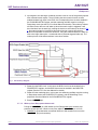
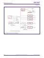
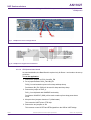
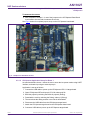
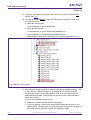
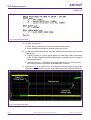
AN11027
Using the LPC1100 low power modes and wake-up times on
the LPCXpresso
Rev. 1 — 7 January 2011
Application note
Document information
Info
Content
Keywords
LPC11xx, LPC11xx(L) and LPC11Cxx , Low Power Modes, Power
Consumption, Wake-up, code example, LPCXpresso
Abstract
This application note introduces the various low power modes of the
LPC11xx series, LPC11xx(L) series, and the LPC11Cxx series, the steps
required to enter the low power modes, wake-up implementation, and
helpful hints to reduce power consumption.
This application note also provides a software example to enter the low
power modes, and demonstrates how to measure the power consumption
and wake-up times using the LPC1114 LPCXpresso board.
AN11027
NXP Semiconductors
Using the LPC1100 low power modes and wake-up times on the
LPCXpresso
Revision history
Rev
Date
Description
1
Initial version.
20110107
Contact information
For additional information, please visit: http://www.nxp.com
For sales office addresses, please send an email to: [email protected]
AN11027
Application note
All information provided in this document is subject to legal disclaimers.
Rev. 1 — 7 January 2011
© NXP B.V. 2011. All rights reserved.
2 of 25
AN11027
NXP Semiconductors
Using the LPC1100 low power modes and wake-up times on the
LPCXpresso
1. Introduction
The LPC1100 microcontroller family is based on the ARM Cortex-M0 CPU architecture
for 8/16-bit microcontroller applications, offering performance, low power, simple
instruction and memory addressing together with reduced code size compared to existing
8/16-bit architectures.
The peripheral complement of the LPC1100 family includes up to 32 kB of flash memory,
up to 8 kB of data memory, one C_CAN controller (LPC11Cxx), one Fast-mode Plus I2C
bus interface, one RS-485/EI-485UART, up to two SPI interfaces with SSP Features,
four general purpose timers, a 10-bit ADC, and up to 42 general purpose I/O pins.
On-chip C_CAN drivers and flash In-System Programming tools via C_CAN are included
on the LPC11Cxx series; in addition, an on-chip, high speed CAN transceiver is available
on the LPC11C2x series.
On-chip power profiles are included on the LPC11xx(L) series.
The LPC1100 family targets a wide range of applications, including eMetering, lighting,
industrial networking, alarm systems, and white goods.
This application note introduces the various low power modes of the LPC11xx,
LPC11xx(L) and LPC11Cxx parts, the steps required to enter the low power modes,
wake-up implementation, and helpful hints to reduce power consumption. This
application note also provides software examples to enter and wake-up from the low
power modes, and demonstrates how to measure the power consumption and wake-up
times using the LPC1114 LPCXpresso board.
The various topics covered in this application note are as follows:
1. Low Power Modes
2. Entering Low Power Modes
3. Wake-Up Implementation
4. Additional hints to reduce power consumption
5. Low power mode demos using the LPC1114 LPCXpresso board
AN11027
Application note
All information provided in this document is subject to legal disclaimers.
Rev. 1 — 7 January 2011
© NXP B.V. 2011. All rights reserved.
3 of 25
AN11027
NXP Semiconductors
Using the LPC1100 low power modes and wake-up times on the
LPCXpresso
2. Low power modes
On the LPC11xx, LPC11xx(L) and LPC11Cxx series, there are three reduced power
modes: Sleep, Deep-Sleep, and Deep Power-down modes. The following sections cover
the features and configurations for the low power modes.
2.1.1 Sleep mode
In Sleep mode, the system clock to the ARM Cortex-M0 core is stopped, and execution
of instructions is suspended until either a reset or an enabled interrupt occurs.
Peripheral functions, if selected to be clocked in the SYSAHBCLKCTRL register,
continue operation during Sleep mode and may generate interrupts to cause the
processor to resume execution. Sleep mode eliminates dynamic power used by the
processor itself, memory systems and their related controllers, and internal buses. The
processor state and registers, peripheral registers, and internal SRAM values are
maintained, and the logic levels of the pins remain static.
2.1.2 Deep-sleep mode
In Deep-sleep mode, the system clock to the processor is disabled as in Sleep mode. All
analog blocks are powered down, except for the BOD circuit and the watchdog oscillator,
which must be selected or deselected during Deep-sleep mode in the PDSLEEPCFG
register. See section 3.5 for more details.
Deep-sleep mode eliminates all power used by the flash, analog peripherals and all
dynamic power used by the processor itself, memory systems and their related
controllers, and internal buses. The processor state and registers, peripheral registers,
and internal SRAM values are maintained, and the logic levels of the pins remain static.
2.1.3 Deep power-down mode
In Deep Power-down mode, power and clocks are shut off to the entire chip with the
exception of the WAKEUP pin.
During Deep power-down mode, the contents of the SRAM and registers are not retained
except for a small amount of data which can be stored in five 32-bit general purpose
registers of the power management unit block.
All functional pins are tri-stated in Deep power-down mode except for the WAKEUP
pin.
3. Entering the low power modes
This section describes the mechanism to put the LPC11xx, LPC11xx(L) and LPC11Cxx
series into the three low power modes (sleep, deep-sleep, deep power-down).
3.1 System Control Register (SCR)
The SCR register controls features of entry to and exit from low power modes.
Sleep mode and Deep Sleep mode are selected by the SLEEPDEEP bit in the CortexM0 System Control Register (SCR).
The bit assignments are shown in Fig 1.
AN11027
Application note
All information provided in this document is subject to legal disclaimers.
Rev. 1 — 7 January 2011
© NXP B.V. 2011. All rights reserved.
4 of 25
AN11027
NXP Semiconductors
Using the LPC1100 low power modes and wake-up times on the
LPCXpresso
019aab347
Fig 1. System Control Register (SCR, 0xE000ED10)
If the SLEEPDEEP bit in the Cortex-M0 System Control Register (SCR) is 0, Sleep mode
is selected.
If the SLEEPDEEP bit in the Cortex-M0 System Control Register (SCR) is 1, Deep-sleep
mode is selected.
3.2 Power Control Register (PCON)
The PCON register selects whether one of the ARM Cortex-M0 controlled power-down
modes (Sleep mode or Deep-Sleep mode) or the Deep power-down mode is entered. It
also provides the flags for Sleep or Deep-sleep modes and Deep power-down modes
respectively. See Fig 2 below.
AN11027
Application note
All information provided in this document is subject to legal disclaimers.
Rev. 1 — 7 January 2011
© NXP B.V. 2011. All rights reserved.
5 of 25
AN11027
NXP Semiconductors
Using the LPC1100 low power modes and wake-up times on the
LPCXpresso
019aab348
Fig 2. Power Mode Control Register (PCON)
3.3 Wait For Interrupt (WFI) instruction
Execution of the WFI instruction will cause immediate entry to any of the low reduced
power modes based on the SLEEPDEEP bit and PCON register settings mentioned
above.
The WFI instruction is a Cortex-M0 instruction which cannot be directly accessible by
ANSI C. The CMSIS (Cortex Microcontroller Software Interface Standard) provides an
intrinsic function to generate a WFI instruction and is supported by C compiler.
If a C compiler does not support the WFI intrinsic function, then the user will have to use
assembly code to execute WFI instruction.
3.4 Programming steps to enter sleep mode
The following steps must be performed to enter sleep mode:
1. The DPDEN bit in the PCON register must be set to zero.
2. The SLEEPDEEP bit in the ARM Cortex-M0 SCR register must be set to zero.
3. Use the ARM Cortex-M0 Wait-For-Interrupt (WFI) instruction.
Fig 3 below shows code example to enter sleep mode.
AN11027
Application note
All information provided in this document is subject to legal disclaimers.
Rev. 1 — 7 January 2011
© NXP B.V. 2011. All rights reserved.
6 of 25
AN11027
NXP Semiconductors
Using the LPC1100 low power modes and wake-up times on the
LPCXpresso
019aab349
Fig 3. Code example (Sleep mode)
3.5 Programming steps to enter Deep-sleep mode
The following steps must be performed to enter Deep-sleep mode:
1. The DPDEN bit in the PCON register must be set to zero.
2. Select the power configuration in Deep-sleep mode in the PDSLEEPCFG register.
This register controls the behavior of the WatchDog (WD) oscillator and the BOD
circuit when the device enters the Deep-sleep mode. This register must be initialized
at least once before entering Deep-sleep mode with one of the four values shown
below. Failure to initialize and program this register correctly may result in undefined
behavior of the microcontroller. The values listed in the Fig 4 below are the only
values allowed for PDSLEEPCFG register.
019aab350
Fig 4. PDSLEEPCFG register settings (Deep-sleep mode)
a. If a timer controlled self wake-up is needed, ensure the watchdog oscillator is
powered in the PDRUNCFG register and switch the clock source to WD oscillator
in the MAINCLKSEL register (see LPC11xx User Manual for details).
b. The watchdog oscillator can be left running in Deep-sleep mode to provide a clock
for the watchdog timer or a general purpose timer if they are needed for selfwake-up purposes. See section 3.7 for more details. In this case, the watchdog
oscillator analog output frequency must be set to its lowest value (bits FREQSEL
in the WDTOSCCTRL = 0001, see LPC11xx User Manual) and all peripheral
clocks other than timer clock must be disabled in the SYSAHBCLKCTRL register
before entering Deep-sleep mode. The watchdog oscillator, if running, contributes
an additional current drain in Deep-sleep mode.
c. If no timer-controlled self wake-up is needed and the watchdog oscillator is shut
down, ensure that the IRC is powered in the PDRUNCFG register and switch the
clock source to IRC in the MAINCLKSEL register before entering deep sleep
mode. This ensures that the system clock is shut down glitch-free (see the
LPC11xx User Manual for details).
AN11027
Application note
All information provided in this document is subject to legal disclaimers.
Rev. 1 — 7 January 2011
© NXP B.V. 2011. All rights reserved.
7 of 25
AN11027
NXP Semiconductors
Using the LPC1100 low power modes and wake-up times on the
LPCXpresso
d. Leaving the BOD circuit enabled will protect the device from a low voltage event
occurring while the micro is in Deep-sleep mode. However, the BOD circuit
causes an additional current drain in Deep-sleep mode.
3. Select the power configuration after wake-up in the PDAWAKECFG register. The bits
in this register can be programmed to determine the state the chip must enter when it
is waking up from Deep-sleep mode.
4. If an external pin is used for wake-up, enable and clear the wake-up pin in the start
logic registers, and enable the interrupt associated to that start logic in the NVIC.
5. In the SYSAHBCTRL register, disable all peripherals except the counter/timer or
WDT if needed.
6. Write one to the SLEEPDEEP bit in the ARM Cortex-M0 SCR register.
7. Use the ARM Cortex-M0 Wait-For-Interrupt (WFI) instruction.
Fig 5 shows code example to enter Deep-sleep mode.
019aab351
Fig 5. Code example (Deep-sleep mode)
AN11027
Application note
All information provided in this document is subject to legal disclaimers.
Rev. 1 — 7 January 2011
© NXP B.V. 2011. All rights reserved.
8 of 25
AN11027
NXP Semiconductors
Using the LPC1100 low power modes and wake-up times on the
LPCXpresso
3.6 Programming steps to enter Deep power-down mode
The following steps must be performed to enter Deep power-down mode:
1. Write one to the DPDEN bit in the PCON register.
2. Store data to be retained in the general purpose registers (see the LPC11xx User
Manual for details).
3. Write one to the SLEEPDEEP bit in the ARM Cortex-M0 SCR register.
4. Ensure that the IRC is powered by setting bits IRCOUT_PD and IRC_PD to zero in
the PDRUNCFG register before entering Deep power-down mode.
5. Use the ARM Cortex-M0 Wait-For-Interrupt (WFI) instruction.
Please note that the WAKEUP pin needs to be externally pulled HIGH before entering
deep power-down mode.
019aab352
Fig 6. Code example (Deep power-down mode)
3.7 Wake-up implementation
The following section describes the wake-up implementation for each low power mode on
the LPC11xx, LPC11xx(L) and LPC11Cxx series.
3.7.1.1 Wake-up from Sleep mode
Sleep mode is exited automatically when an interrupt enabled by the NVIC arrives at the
processor or a reset occurs. Please see the LPC11xx User Manual for details on which
interrupt sources are connected to NVIC. After wake-up due to an interrupt, the
microcontroller returns to its original power configuration defined by the contents of the
PDRUNCFG and the SYSAHBCLKDIV registers. If a reset occurs, the microcontroller
enters the default configuration in Active mode.
3.7.1.2 Wake-up from Deep-sleep mode
The microcontroller can wake up from Deep-sleep mode in the following ways:
1. Signal on an external pin which is connected to start logic. For this purpose, certain
port pins can be enabled as inputs to the start logic. Please see the LPC11xx User
Manual for which port pins are connected to the start logic and serve as wake-up
pins. The start logic does not require any clocks and generates the interrupt if
enabled in the NVIC to wake up from Deep-sleep mode.
AN11027
Application note
All information provided in this document is subject to legal disclaimers.
Rev. 1 — 7 January 2011
© NXP B.V. 2011. All rights reserved.
9 of 25
AN11027
NXP Semiconductors
Using the LPC1100 low power modes and wake-up times on the
LPCXpresso
2. Input signal to the start logic created by a match event on one of the general purpose
timer external match outputs. The pin holding the timer match function must be
enabled as start logic input in the NVIC, the corresponding timer must be enabled in
the SYSAHBCLKCTRL register, and the watchdog oscillator must be running in
Deep-sleep mode (see the LPC11xx User Manual for details). This wake-up scheme
will allow for the device to self wake-up when the match output is triggered. It will
then feed back into the start logic causing the device to self wake-up as shown in Fig
7. No external trigger is required for this method and as a result, this reduces
external components on the board. However, using this method causes the wake-up
time to be longer than option 1 mentioned above (external triggered wake-up). The
wake-up times will be discussed later in the demo section.
019aab369
Fig 7. Self wake-up diagram
3. Reset from the BOD circuit. In this case, the BOD circuit must be enabled in the
PDSLEEPCFG register, and the BOD reset must be enabled in the BODCTRL
register (See the LPC11xx User Manual for details).
4. Reset from the watchdog timer. In this case, the watchdog oscillator must be running
in Deep-sleep mode (see PDSLEEPCFG register), and the WatchDog Timer
peripheral must be enabled in the SYSAHBCLKCTRL register.
5. External RESET pin.
3.7.1.3 Wake-up from Deep power-down mode
Pulling the WAKEUP pin LOW wakes up from Deep power-down, and the chip
performs a reset process. Minimum low pulse width for WAKEUP pin is 50 ns.
1. WAKEUP is generated when an external HIGH to LOW transition occurs on the
WAKEUP pin (level-sensitive).
AN11027
Application note
All information provided in this document is subject to legal disclaimers.
Rev. 1 — 7 January 2011
© NXP B.V. 2011. All rights reserved.
10 of 25
AN11027
NXP Semiconductors
Using the LPC1100 low power modes and wake-up times on the
LPCXpresso
a. The Power Management Unit (PMU) will turn on the on-chip voltage regulator.
When the core voltage reaches the power-on-reset (POR) trip point, a system
reset will be triggered and the chip re-boots.
b. All registers except the GPREG0 to GPREG4 and PCON will be in their reset
state.
2. Once the chip has booted, the deep power-down flag can be read in the PCON
register to verify that the reset was caused by a wake-up event from Deep powerdown.
3. Clear the deep power-down flag in the PCON register.
4. (Optional) Read the stored data in the general purpose registers.
Please note that the RESET pin has no functionality in Deep power-down mode.
3.8 Additional tips to reduce power consumption
The current consumption can be further reduced by considering the following points:
3.8.1.1 CPU clock rate
The CPU clock rate can be controlled as needed, which allows a trade-off of power
versus processing speed based on application requirements.
1. Changing clock sources: Internal Oscillator (12 MHz +/− 1 %), System Oscillator
(1 MHz to 25 MHz), Watchdog Oscillator (7.8 kHz to 1.7 MHz +/− 40 %).
2. Reconfiguring PLL values, and/or altering the AHB Clock Divider (SYSAHBCLKDIV)
value.
3. Lowering the PLL’s output frequency (FCCO, 156 MHz to 320 MHz) can also save
power.
4. An 8-bit system AHB clock divider register (SYSAHBCLKDIV) allows a range of
options, including slowing CPU operation to a low rate for temporary power savings
without turning off SYS PLL. See Fig 8 below.
AN11027
Application note
All information provided in this document is subject to legal disclaimers.
Rev. 1 — 7 January 2011
© NXP B.V. 2011. All rights reserved.
11 of 25
AN11027
NXP Semiconductors
Using the LPC1100 low power modes and wake-up times on the
LPCXpresso
019aab370
Fig 8. Clock Generation Unit (CGU) diagram
AN11027
Application note
All information provided in this document is subject to legal disclaimers.
Rev. 1 — 7 January 2011
© NXP B.V. 2011. All rights reserved.
12 of 25
AN11027
NXP Semiconductors
Using the LPC1100 low power modes and wake-up times on the
LPCXpresso
3.9 System AHB Clock Control Register (AHBCLKCTRL)
As shown in the Fig 8, the SYSAHBCLKCTRL register enables the clocks to individual
system and peripheral blocks. Depending upon application requirements, the user can
use this register to reduce power by disabling clocks to unused peripherals. See the
LPC11xx User Manual for details.
3.10 Peripheral clock dividers
Selected peripherals have their own clock divider (SPI0CLKDIV, UARTCLKDIV,
SPI1CLKDIV, WDTCLKDIV, CLKOUTDIV) which controls the rate of the peripheral clock
signal that will be supplied to the corresponding peripheral (see Fig 8). Depending on
application requirements, the user can use these divider registers to reduce the
peripheral clock frequency or shut down the clock to reduce power. See the LPC11xx
User Manual for details.
3.11 Power-down Configuration register (PDRUNCFG)
PDRUNCFG Register contains control bits that power on or off individual analog blocks,
allowing elimination of power consumption by analog peripherals that are not needed.
See the LPC11xx User Manual for details.
3.12 Miscellaneous
3.12.1 Software
Most embedded applications terminate with a while(1) loop, and they service interrupts
whenever needed. In this case, code is still constantly fetched from the on-chip flash and
executed which adds to the power consumption. A better solution would be to switch to
the sleep power saving mode and then wait for interrupts. An interrupt from a peripheral
would then wake the device from Sleep mode. Considerable power savings can be
achieved by keeping the core in Sleep mode while it is waiting for interrupts.
3.12.2 Port pins
Additional steps can be used to reduce current consumption on the IO current in the low
power modes. The general purpose port pins on the LPC11xx, LPC11xx(L) and
LPC11Cxx series have programmable internal pull-ups enabled by default. Before
entering low power modes, reduce the IO current as follows:
1. All General Purpose I/O pins (GPIO) default to input with pull-up resistor enabled.
Using the IOCON registers, first, disable the internal pull-ups on all general port pins.
Second, configure the IOs as GPIO outputs and drive them low. Make sure the pins
are not being externally pulled high, OR
2. All General Purpose I/O pins (GPIO) default to input with pull-up resistor enabled.
Using the IOCON registers, first, disable the internal pull-ups on all general port pins.
Second, configure the IOs as GPIO outputs and drive them high. Make sure the pins
are not being externally pulled low, OR
3. Using the IOCON registers, first disable the internal pull-ups on all general port pins.
Second, configure the IOs as GPIO inputs and using an external resistor, pull the IOs
high or low.
Please note that in deep power-down mode, state of the port pins does not affect the
current consumption and the steps mentioned above do not need to be considered in this
mode.
AN11027
Application note
All information provided in this document is subject to legal disclaimers.
Rev. 1 — 7 January 2011
© NXP B.V. 2011. All rights reserved.
13 of 25
AN11027
NXP Semiconductors
Using the LPC1100 low power modes and wake-up times on the
LPCXpresso
3.12.3 CAN pins
On the LPC11C1x devices, when not using the CAN device, the CAN pins (CAN_RXD
and CAN_TXD) should be externally pulled low to reduce the IO current.
3.12.4 RESET_N/PIO0_0 pin
On the LPC11xx, LPC11xx(L) and LPC11Cxx parts, the RESET /PIO0_0 pin needs to
be externally pulled up via 10k – 47k resistor when in deep power-down mode. If the pin
is left floating, user will see an increase in current consumption.
3.12.5 Debug notes
The user should be aware of certain limitations during debugging. The most important is
that, due to limitations of the Cortex-M0 integration, the LPC11xx, LPC11xx(L) and
LPC11Cxx parts cannot wake up in the usual manner from Sleep, Deep Sleep, or Deep
power-down modes. It is recommended not to use these modes during debug. Once an
application is downloaded via SWD interface, the USB to SWD debug adapter should be
removed from the target board. Another issue is that debug mode changes the way in
which reduced power modes are handled by the Cortex-M0 CPU. This causes power
modes at the device level to be different from normal modes operation. These
differences mean that power measurements should not be made while debugging; the
results will be higher than during normal operation in an application.
AN11027
Application note
All information provided in this document is subject to legal disclaimers.
Rev. 1 — 7 January 2011
© NXP B.V. 2011. All rights reserved.
14 of 25
AN11027
NXP Semiconductors
Using the LPC1100 low power modes and wake-up times on the
LPCXpresso
4. Low power mode demos
4.1 Objective
This application note provides two low power mode examples using the LPCXpresso
platform:
Demo 1: Low Power Modes (sleep, deep sleep, deep power-down) using the
UART interface.
This example allows the user to enter the low power modes and wake-up using
an external port pin.
Demo2: Self Wake-up Demo
This example configures the watchdog oscillator at lowest frequency to clock the
16-bit Timer 0 in run mode and deep-sleep mode. The device generates a
repetitive self wake-up from deep-sleep mode and toggles a port pin when in run
mode.
Both examples show the user how to measure the current and wake-up times. The
following sections provide the necessary steps to set-up the low power mode demos on
the LPCXpresso platform. Both project demos are CMSIS (Cortex Microcontroller
Software Interface Standard) compliant.
4.2 LPCXpresso demonstrations
4.2.1.1 Requirements
1. LPCXpresso IDE.
2. LPCXpresso Target Board (LPC1114) (see Fig 9).
3. LPCXpresso Base Board (see Fig 11)
The LPCXpresso Base Board contains a USB-to-Serial bridge chip (FT232R from FTDI)
that connects the UART channel on the LPCXpresso target LPC1114 to a virtual COM
port on the PC (via USB).
Please note that the Base Board is required only for Demo 1 which uses UART interface
to display a power mode selection menu.
4.2.1.2 Terminal window
For Demo 1, terminal window like TeraTerm or HyperTerminal window is needed to
display the options to enter low power modes.
4.2.1.3 LPCXpresso target board (LPC1114)
To measure the current:
The LPCXpresso Target Board requires the following set-up for both demos:
1. The LPCXpresso target board includes an integrated JTAG debugger (LPC-Link). By
default, the power is shared between the LPC1114 and LPC-Link. Trace connection
between J4.1 and J4.2 needs to be cut to separate the power supply and thereafter,
a user can connect an external supply on J4.2 to measure the current using an
ammeter. The current should be measured at the VIO_3V3X which supplies the
power to the LPC1114. See Fig 9 below.
2. Since the software example is configuring all the pins as GPIO outputs and driving
the GPIOs low, the external 12K pull-up resistor on RESET /PIO0_0 needs to be
removed. See Fig 9 below.
AN11027
Application note
All information provided in this document is subject to legal disclaimers.
Rev. 1 — 7 January 2011
© NXP B.V. 2011. All rights reserved.
15 of 25
AN11027
NXP Semiconductors
Using the LPC1100 low power modes and wake-up times on the
LPCXpresso
019aab371
Fig 9. LPCXpresso LPC1114 target board
019aab372
Fig 10. LPCXpresso target board schematics
4.2.1.4 LPCXpresso base board
As mentioned before, the Base Board is required only for Demo 1 and needs to be set-up
as follows:
To run the application:
1. Remove the jumpers on PIO0_2 and BL_EN
2. Put a jumper between PIO0_2 and BL_EN
PIO0_2 is used as wake-up source for sleep and deep sleep.
Push button ‘BL_EN’ (SW3) will be used for sleep and deep sleep.
3. Remove the jumper on PIO1_4.
PIO1_4 is multiplexed with WAKEUP functionality.
Push button ‘WAKEUP’ (SW2) will be used to wake-up from deep power-down
mode.
4. Keep the three jumpers closed on J7 (default state).
This routes the UART pins to FTDI chip.
5. Remove the two jumpers on J54
This removes control of DTR and RTS signals from the USB to UART bridge.
AN11027
Application note
All information provided in this document is subject to legal disclaimers.
Rev. 1 — 7 January 2011
© NXP B.V. 2011. All rights reserved.
16 of 25
AN11027
NXP Semiconductors
Using the LPC1100 low power modes and wake-up times on the
LPCXpresso
To measure the current:
6. After completion of steps 1-4, rest of the jumpers on the LPCXpresso Base Board
would need to be removed to measure the current.
See Fig 11 below for complete jumper set-up on the LPCXpresso base board.
019aab373
Fig 11. LPCXpresso Base Board board
4.2.1.5 LPCXpresso Application Set-up for Demo 1
As mentioned before, demo 1 allows the user to enter the low power modes using UART
interface, and wake-up using an external port pin.
Application is set-up as follows:
1. Connect the USB cable to power up the LPCXpresso LPC1114 target board.
2. Open LPCXpresso IDE and import LPC1100 wakeup.zip file.
3. Build the project by selecting the Build ‘all projects’ (Debug).
4. Download the code by selecting the Debug ‘wake-up’ (Debug).
5. Then terminate the debug session once code is downloaded.
6. Disconnect the USB cable from the LPCXpresso target board.
7. Attach the LPCXpresso target board to the LPCXpresso base board.
8. Connect a USB cable to power up the LPCXpresso target board.
AN11027
Application note
All information provided in this document is subject to legal disclaimers.
Rev. 1 — 7 January 2011
© NXP B.V. 2011. All rights reserved.
17 of 25
AN11027
NXP Semiconductors
Using the LPC1100 low power modes and wake-up times on the
LPCXpresso
9. Connect a USB cable to the USB to UART connector. (on the LPCXpresso Base
Board). See Fig 11.
10. User will be prompted twice to install the FTDI drivers for the USB to Serial chip
(FT232R) to function.
a. Select the following path:
C:\nxp\lpcxpresso_3.3\Drivers\RedProbe
b. Select the following files:
C:\nxp\lpcxpresso_3.3\Drivers\RedProbe\i386\ftdibus.sys
C:\nxp\lpcxpresso_3.3\Drivers\RedProbe\i386\ftser2k.sys
c. Once installed, should see the following in device manager/properties (Fig 12):
019aab374
Fig 12. USB Serial Port / Converter
11. Some terminal programs need a low COM port number, for example between 1 and
5. Very often the COM port number for the USB Serial Port is higher than this,
therefore this needs to be changed manually. If this is the case, then follow the
additional steps as below. Further details can be found in the LPCXpresso Base
Board User’s Guide.
a. Go to Device Manager and Ports List.
b. Right click on USB Serial Port and select Properties.
c. Go to Port Settings > Advanced to change COM Port Number as shown in the
diagram below. COM port number will vary depending on the terminal program. In
this example below, COM port number was changed to COM4.
AN11027
Application note
All information provided in this document is subject to legal disclaimers.
Rev. 1 — 7 January 2011
© NXP B.V. 2011. All rights reserved.
18 of 25
AN11027
NXP Semiconductors
Using the LPC1100 low power modes and wake-up times on the
LPCXpresso
019aab375
Fig 13. Changing the COM number for USB serial port
12. Demo 1 uses the terminal program and the settings for the serial port are shown in
Fig 14.
019aab376
Fig 14. Terminal program set-up
13. Hit RESET button.
14. The output of the code is shown in Fig 15. The menu below shows how to enter the
three low power modes (use lower case to enter modes).
AN11027
Application note
All information provided in this document is subject to legal disclaimers.
Rev. 1 — 7 January 2011
© NXP B.V. 2011. All rights reserved.
19 of 25
AN11027
NXP Semiconductors
Using the LPC1100 low power modes and wake-up times on the
LPCXpresso
019aab377
Fig 15. Low power mode demo
15. To wake up the device:
a. Press ‘BL_EN’ push button to exit sleep and deep-sleep modes.
b. Press WAKEUP push button to exit deep power-down mode.
16. For Sleep and Deep Sleep modes, the wake-up times can be measured by using the
following pins:
a. Trigger pin (PIO0_2) - Used to get the device out of the sleep mode or deep-sleep
mode. The pin is triggered externally (falling edge) to wake the device up using an
external push button.
b. Strobe pin (PIO2_0) – After wake-up, the device returns into run mode, and this
pin is set high within the WAKEUP_IRQHANDLER() subroutine.
17. As shown in Fig 16, the wakeup time is the difference between the falling edge of the
trigger pin (yellow waveform) and the rising edge of the Strobe pin (green waveform).
019aab378
Fig 16. Low power mode demo
AN11027
Application note
All information provided in this document is subject to legal disclaimers.
Rev. 1 — 7 January 2011
© NXP B.V. 2011. All rights reserved.
20 of 25
AN11027
NXP Semiconductors
Using the LPC1100 low power modes and wake-up times on the
LPCXpresso
4.2.1.6 Power measurements and Wake-Up measurements using Demo 1
Table 1 shows the typical power consumption and wake-up measurements using demo
1.
Table 1.
Typical power consumption (3.3 V, Temp = 25 °C)
Low power modes
Ivdd current
Wake-up
Sleep mode (IRC (12 MHz), all
peripherals off)
2 mA
4.7 μs
Sleep mode (System Osc (12 MHz), all
peripherals off)
2 mA
4.7 μs
Sleep mode (System Osc with PLL
enabled (50 MHz), all peripherals off)
6 mA
1.18 μs
2 μA (LPC11xx(L) series)
56 μs
Deep-sleep Mode (Watchdog Osc off
and BOD off)
6 μA (LPC 11xx and LPC11Cxx series)
Deep Power-down Mode (note 1)
220 nA
240 μs
Note 1: Wake-up from deep power-down behaves like a chip reset. Demos provided with
this application note are not readily set-up to measure the wake-up time for deep powerdown mode. Using demo 1, user can set the strobe pin to be high in the reset handler
(See the cr_startup_lpc11.c source file). The time between when the WAKEUP pin is
triggered (goes low) and when the strobe pin goes high in the reset handler is the wakeup time for deep power-down mode.
4.2.1.7 LPCXpresso Application Set-up for Demo 2
As mentioned before, demo 2 configures the watchdog oscillator at lowest frequency to
clock the 16-bit Timer 0 in run and deep sleep modes. The device generates a repetitive
self wake-up from deep-sleep mode and toggles a port pin when in run mode.
Application is set-up as follows:
1. Connect the USB cable to power up the LPCXpresso target board.
2. Open LPCXpresso IDE and import LPC1100 self wakeup.zip file
3. Build the project by selecting the Build ‘all projects’ (Debug)
4. Download the code by selecting the Debug ‘wake-up’ (Debug)
5. Then terminate the debug session once code is downloaded.
6. Power cycle the LPCXpresso target board.
7. The wake-up time can be measured by using the following pins:
a. Trigger pin (PIO0_8/CT16B0_MAT0) – Timer Output to get the device out of the
deep-sleep mode.
b. Strobe pin (PIO0_7) – After wake-up, the device returns into run mode, and this
pin is toggles 4 times within the WAKEUP_IRQHANDLER() subroutine.
8. Fig 17 shows the waveform output of the Timer match output and GPIO pin.
AN11027
Application note
All information provided in this document is subject to legal disclaimers.
Rev. 1 — 7 January 2011
© NXP B.V. 2011. All rights reserved.
21 of 25
AN11027
NXP Semiconductors
Using the LPC1100 low power modes and wake-up times on the
LPCXpresso
019aab379
Fig 17. Low power mode self-wakeup demo
9. As shown in Fig 18, the wakeup time is the difference between the rising edge of the
trigger pin and the first falling edge of the Strobe pin.
019aab380
Fig 18. Low power mode self-wakeup demo
10. Please note that once the code for demo 2 is downloaded, the device enters and
exits deep-sleep mode on a repetitive basis. User must put the device first in ISP
mode to erase or re-program the flash. See the LPC11xx User Manual for details on
how to enter ISP mode.
4.2.1.8
Power measurements and Wake-Up Measurements using Demo 2
Table 2 shows the typical power consumption and self wake-up measurements using
demo 2.
AN11027
Application note
All information provided in this document is subject to legal disclaimers.
Rev. 1 — 7 January 2011
© NXP B.V. 2011. All rights reserved.
22 of 25
AN11027
NXP Semiconductors
Using the LPC1100 low power modes and wake-up times on the
LPCXpresso
Table 2.
Typical power consumption (3.3V, Temp = 25 °C)
Low power modes
Ivdd current
Deep-Sleep mode (Watchdog Oscillator
(8.8 kHz) enabled, 16-bit Timer 0 on, BOD
off)
Wake-up
3 μA (LPC11xx(L) series)
7.0 ms
7 μA (LPC 11xx and LPC11Cxx series)
5. Conclusion
In conclusion, the LPC11xx, LPC11xx(L) and LPC11Cxx series provides great flexibility
and various options for users to achieve low power consumption and wake-up flexibility.
As shown in Table 1, the user has various low power mode options to choose from in
order to achieve the desired power consumption by trading up or down wake-up time of
the device. This flexibility allows a trade-off between power consumption and wake-up
speed based on the user’s application requirements.
In addition, user has the option of using the self wake-up feature and would not require
an external component to wake the device up from deep sleep mode. With the self wakeup feature, user can still achieve low power consumption but the trade off will be a longer
wake-up time as shown in Table 2. To achieve a faster wake-up time for deep-sleep
mode, the user will need an external event trigger, switch the clock source to IRC before
going into deep sleep mode and turn the Watchdog Oscillator off in deep-sleep mode.
AN11027
Application note
All information provided in this document is subject to legal disclaimers.
Rev. 1 — 7 January 2011
© NXP B.V. 2011. All rights reserved.
23 of 25
AN11027
NXP Semiconductors
Using the LPC1100 low power modes and wake-up times on the
LPCXpresso
6. Legal information
NXP Semiconductors products in such equipment or applications and
therefore such inclusion and/or use is at the customer’s own risk.
6.1 Definitions
Draft — The document is a draft version only. The content is still under
internal review and subject to formal approval, which may result in
modifications or additions. NXP Semiconductors does not give any
representations or warranties as to the accuracy or completeness of
information included herein and shall have no liability for the consequences
of use of such information.
6.2 Disclaimers
Limited warranty and liability — Information in this document is believed to
be accurate and reliable. However, NXP Semiconductors does not give any
representations or warranties, expressed or implied, as to the accuracy or
completeness of such information and shall have no liability for the
consequences of use of such information.
In no event shall NXP Semiconductors be liable for any indirect, incidental,
punitive, special or consequential damages (including - without limitation lost profits, lost savings, business interruption, costs related to the removal
or replacement of any products or rework charges) whether or not such
damages are based on tort (including negligence), warranty, breach of
contract or any other legal theory.
Notwithstanding any damages that customer might incur for any reason
whatsoever, NXP Semiconductors’ aggregate and cumulative liability
towards customer for the products described herein shall be limited in
accordance with the Terms and conditions of commercial sale of NXP
Semiconductors.
Right to make changes — NXP Semiconductors reserves the right to make
changes to information published in this document, including without
limitation specifications and product descriptions, at any time and without
notice. This document supersedes and replaces all information supplied prior
to the publication hereof.
Applications — Applications that are described herein for any of these
products are for illustrative purposes only. NXP Semiconductors makes no
representation or warranty that such applications will be suitable for the
specified use without further testing or modification.
Customers are responsible for the design and operation of their applications
and products using NXP Semiconductors products, and NXP
Semiconductors accepts no liability for any assistance with applications or
customer product design. It is customer’s sole responsibility to determine
whether the NXP Semiconductors product is suitable and fit for the
customer’s applications and products planned, as well as for the planned
application and use of customer’s third party customer(s). Customers should
provide appropriate design and operating safeguards to minimize the risks
associated with their applications and products.
NXP Semiconductors does not accept any liability related to any default,
damage, costs or problem which is based on any weakness or default in the
customer’s applications or products, or the application or use by customer’s
third party customer(s). Customer is responsible for doing all necessary
testing for the customer’s applications and products using NXP
Semiconductors products in order to avoid a default of the applications and
the products or of the application or use by customer’s third party
customer(s). NXP does not accept any liability in this respect.
Export control — This document as well as the item(s) described herein
may be subject to export control regulations. Export might require a prior
authorization from national authorities.
6.3 Trademarks
Notice: All referenced brands, product names, service names and
trademarks are property of their respective owners.
Suitability for use — NXP Semiconductors products are not designed,
authorized or warranted to be suitable for use in life support, life-critical or
safety-critical systems or equipment, nor in applications where failure or
malfunction of an NXP Semiconductors product can reasonably be expected
to result in personal injury, death or severe property or environmental
damage. NXP Semiconductors accepts no liability for inclusion and/or use of
AN11027
Application note
All information provided in this document is subject to legal disclaimers.
Rev. 1 — 7 January 2011
© NXP B.V. 2011. All rights reserved.
24 of 25
AN11027
NXP Semiconductors
Using the LPC1100 low power modes and wake-up times on the
LPCXpresso
7. Contents
1.
2.
2.1.1
2.1.2
2.1.3
3.
3.1
3.2
3.3
3.4
3.5
3.6
3.7
3.7.1.1
3.7.1.2
3.7.1.3
3.8
3.8.1.1
3.9
3.10
3.11
3.12
3.12.1
3.12.2
3.12.3
3.12.4
3.12.5
4.
4.1
4.2
4.2.1.1
4.2.1.2
4.2.1.3
4.2.1.4
4.2.1.5
4.2.1.6
4.2.1.7
4.2.1.8
5.
6.
Introduction .........................................................3
Low power modes ...............................................4
Sleep mode ........................................................4
Deep-sleep mode...............................................4
Deep power-down mode ....................................4
Entering the low power modes ..........................4
System Control Register (SCR) .........................4
Power Control Register (PCON) ........................5
Wait For Interrupt (WFI) instruction ....................6
Programming steps to enter sleep mode ...........6
Programming steps to enter Deep-sleep mode..7
Programming steps to enter Deep power-down
mode ..................................................................9
Wake-up implementation....................................9
Wake-up from Sleep mode.................................9
Wake-up from Deep-sleep mode .......................9
Wake-up from Deep power-down mode........... 10
Additional tips to reduce power consumption ...11
CPU clock rate .................................................11
System AHB Clock Control Register
(AHBCLKCTRL) ...............................................13
Peripheral clock dividers ..................................13
Power-down Configuration register
(PDRUNCFG) ..................................................13
Miscellaneous ..................................................13
Software ...........................................................13
Port pins ...........................................................13
CAN pins ..........................................................14
RESET_N/PIO0_0 pin......................................14
Debug notes.....................................................14
Low power mode demos...................................15
Objective ..........................................................15
LPCXpresso demonstrations............................15
Requirements...................................................15
Terminal window ..............................................15
LPCXpresso target board (LPC1114) ..............15
LPCXpresso Base Board .................................16
LPCXpresso Application Set-up for Demo 1 ....17
Power measurements and Wake-Up
measurements using Demo 1 ..........................21
LPCXpresso Application Set-up for Demo 2 ....21
Power measurements and Wake-Up
Measurements using Demo 2 ..........................22
Conclusion.........................................................23
Legal information ..............................................24
6.1
6.2
6.3
7.
Definitions.........................................................24
Disclaimers.......................................................24
Trademarks ......................................................24
Contents .............................................................25
Please be aware that important notices concerning this document and the product(s)
described herein, have been included in the section 'Legal information'.
© NXP B.V. 2011.
All rights reserved.
For more information, please visit: http://www.nxp.com
For sales office addresses, please send an please send an email to:
[email protected]
Date of release: 7 January 2011
Document identifier: AN11027