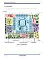
1
User Manual 32 RH850/F1x StarterKit User Manual: Hardware RENESAS MCU RH850 F-Series Y-ASK-RH850F1L All information contained in these materials, including products and product specifications, represents information on the product at the time of publication and is subject to change by Renesas Electronics Corp. without notice. Please review the latest information published by Renesas Electronics Corp. through various means, including the Renesas Electronics Corp. website (http://www.renesas.com). April 2014 RH850/F1x StarterKit User Manual Notice 1. All information included in this document is current as of the date this document is issued. Such information, however, is subject to change without any prior notice. Before purchasing or using any Renesas Electronics products listed herein, please confirm the latest product information with a Renesas Electronics sales office. Also, please pay regular and careful attention to additional and different information to be disclosed by Renesas Electronics such as that disclosed through our website. 2. Renesas Electronics does not assume any liability for infringement of patents, copyrights, or other intellectual property rights of third parties by or arising from the use of Renesas Electronics products or technical information described in this document. No license, express, implied or otherwise, is granted hereby under any patents, copyrights or other intellectual property rights of Renesas Electronics or others. 3. You should not alter, modify, copy, or otherwise misappropriate any Renesas Electronics product, whether in whole or in part. 4. Descriptions of circuits, software and other related information in this document are provided only to illustrate the operation of semiconductor products and application examples. You are fully responsible for the incorporation of these circuits, software, and information in the design of your equipment. Renesas Electronics assumes no responsibility for any losses incurred by you or third parties arising from the use of these circuits, software, or information. 5. When exporting the products or technology described in this document, you should comply with the applicable export control laws and regulations and follow the procedures required by such laws and regulations. You should not use Renesas Electronics products or the technology described in this document for any purpose relating to military applications or use by the military, including but not limited to the development of weapons of mass destruction. Renesas Electronics products and technology may not be used for or incorporated into any products or systems whose manufacture, use, or sale is prohibited under any applicable domestic or foreign laws or regulations. 6. Renesas Electronics has used reasonable care in preparing the information included in this document, but Renesas Electronics does not warrant that such information is error free. Renesas Electronics assumes no liability whatsoever for any damages incurred by you resulting from errors in or omissions from the information included herein. 7. Renesas Electronics products are classified according to the following three quality grades: “Standard”, “High Quality”, and “Specific”. The recommended applications for each Renesas Electronics product depends on the product’s quality grade, as indicated below. You must check the quality grade of each Renesas Electronics product before using it in a particular application. You may not use any Renesas Electronics product for any application categorized as “Specific” without the prior written consent of Renesas Electronics. Further, you may not use any Renesas Electronics product for any application for which it is not intended without the prior written consent of Renesas Electronics. Renesas Electronics shall not be in any way liable for any damages or losses incurred by you or third parties arising from the use of any Renesas Electronics product for an application categorized as “Specific” or for which the product is not intended where you have failed to obtain the prior written consent of Renesas Electronics. The quality grade of each Renesas Electronics product is “Standard” unless otherwise expressly specified in a Renesas Electronics data sheets or data books, etc. “Standard”: Computers; office equipment; communications equipment; test and measurement equipment; audio and visual equipment; home electronic appliances; machine tools; personal electronic equipment; and industrial robots. “High Quality”: Transportation equipment (automobiles, trains, ships, etc.); traffic control systems; anti-disaster systems; anti- crime systems; safety equipment; and medical equipment not specifically designed for life support. “Specific”: Aircraft; aerospace equipment; submersible repeaters; nuclear reactor control systems; medical equipment or systems for life support (e.g. artificial life support devices or systems), surgical implantations, or healthcare intervention (e.g. excision, etc.), and any other applications or purposes that pose a direct threat to human life. 8. You should use the Renesas Electronics products described in this document within the range specified by Renesas Electronics, especially with respect to the maximum rating, operating supply voltage range, movement power voltage range, heat radiation characteristics, installation and other product characteristics. Renesas Electronics shall have no liability for malfunctions or damages arising out of the use of Renesas Electronics products beyond such specified ranges. 9. Although Renesas Electronics endeavors to improve the quality and reliability of its products, semiconductor products have specific characteristics such as the occurrence of failure at a certain rate and malfunctions under certain use conditions. Further, Renesas Electronics products are not subject to radiation resistance design. Please be sure to implement safety measures to guard them against the possibility of physical injury, and injury or damage caused by fire in the event of the failure of a Renesas Electronics product, such as safety design for hardware and software including but not limited to redundancy, fire control and malfunction prevention, appropriate treatment for aging degradation or any other appropriate measures. Because the evaluation of microcomputer software alone is very difficult, please evaluate the safety of the final products or system manufactured by you. 10. Please contact a Renesas Electronics sales office for details as to environmental matters such as the environmental compatibility of each Renesas Electronics product. Please use Renesas Electronics products in compliance with all applicable laws and regulations that regulate the inclusion or use of controlled substances, including without limitation, the EU RoHS Directive. Renesas Electronics assumes no liability for damages or losses occurring as a result of your noncompliance with applicable laws and regulations. 11. This document may not be reproduced or duplicated, in any form, in whole or in part, without prior written consent of Renesas Electronics. 12. Please contact a Renesas Electronics sales office if you have any questions regarding the information contained in this document or Renesas Electronics products, or if you have any other inquiries. (Note 1) “Renesas Electronics” as used in this document means Renesas Electronics Corporation and also includes its majority- owned subsidiaries. (Note 2) “Renesas Electronics product(s)” means any product developed or manufactured by or for Renesas Electronics. R20UT2940ED0100_RH850F1x April 2014 Page 2 RH850/F1x StarterKit User Manual Table of Contents 1. Introduction ............................................................................................................................ 4 2. Quick Start Information ......................................................................................................... 6 2.1 2.2 3. StarterKit Hardware ............................................................................................................. 10 3.1 3.2 3.3 4. Connector and jumper overview ............................................................................................... 6 Board Overview (RH850/F1L Version)....................................................................................... 9 StarterKit Versions .................................................................................................................... 10 Power Supply............................................................................................................................. 10 Functional Areas ....................................................................................................................... 11 3.3.1 Microcontroller Area and Port Pin Interfaces ........................................................................ 12 3.3.2 Power Supply Area ................................................................................................................... 12 3.3.3 LEDs ........................................................................................................................................... 13 3.3.4 Digital inputs for Low Power Sampler (LPS)......................................................................... 14 3.3.5 Pushbutton Switches ................................................................................................................ 15 3.3.6 Analog Input - Potentiometers ................................................................................................ 15 3.3.7 Serial Communication Interfaces ........................................................................................... 16 3.3.8 On-chip Debug and Flash Programming Connector ........................................................... 19 Development tools ............................................................................................................... 20 4.1 4.2 E1 On-Chip Debug Emulator .................................................................................................... 20 Compiler and Debugger Software ........................................................................................... 20 5. RH850/F1L StarterKit Example Software ............................................................................ 21 6. Component Placement And Schematics ............................................................................ 25 6.1 6.2 7. Component placement.............................................................................................................. 25 Schematics ................................................................................................................................ 26 Revision History ................................................................................................................... 27 R20UT2940ED0100_RH850F1x April 2014 Page 3 RH850/F1x StarterKit User Manual 1. Introduction The ‘RH850/F1x StarterKit’ serves as a simple and easy to use platform for evaluating the features and performance of Renesas Electronics’ 32-bit RH850/F1x microcontrollers. Features: Connections for on-chip debugging and flash memory programming Access to all microcontroller I/O pins User interaction through potentiometer, buttons and LEDs Serial interface connections for RS232, LIN and CAN Power supply by RENESAS E1 On-Chip debugger or externally (12V DC input) Support of different RH850/F1x family members (RH850/F1L, RH850/F1M and RH850/F1H) This document will describe the functionality provided by the StarterKit and guide the user through its operation. For details regarding the operation of the microcontroller refer to the RH850/F1x User Manuals. For updates of the StarterKit software and documentation please check: http://www.renesas.eu/updates?id=527 R20UT2940ED0100_RH850F1x April 2014 Page 4 RH850/F1x StarterKit User Manual CAUTION 1. Do not look into the LED beam! Special care must be taken with the high power LEDs 2. When power supply of E1 On-Chip debugger is used please note that the maximum current provided by the debugger is limited to 200mA. Thus an external power supply is required in case all functions on the StarterKit are used to full extend. 3. The High Power LEDs can only be used when the board is supplied by 12V externally. R20UT2940ED0100_RH850F1x April 2014 Page 5 RH850/F1x StarterKit User Manual 2. Quick Start Information 2.1 Connector and jumper overview J1 Pin J2 Function Pin Pin P11_1 P11_2 2 1 3 P11_3 P11_4 4 3 5 P11_5 P11_6 6 5 7 P11_7 P11_8 8 7 9 P11_9 P11_10 10 9 11 P11_11 P11_12 12 11 13 P11_13 P11_14 14 13 15 P11_15 P0_0 16 15 17 P0_1 P0_2 18 17 19 P0_3 P0_4 20 19 21 P0_5 P0_6 22 21 23 P0_7 P0_8 24 23 25 P0_9 P0_10 26 25 27 P0_11 P0_12 28 27 29 P0_13 P0_14 30 29 31 JP0_6 JP0_5 32 31 33 JP0_4 JP0_3 34 33 35 JP0_2 JP0_1 36 35 37 JP0_0 P1_15 38 37 39 GND VDD 40 39 1 Table 1. R20UT2940ED0100_RH850F1x April 2014 Function P12_5 P11_0 P12_3 P12_4 P12_1 P12_2 P10_15 P12_0 P10_13 P10_14 P10_11 P10_12 P10_9 P10_10 P10_7 P10_8 P10_5 P10_6 P10_3 P10_4 P10_1 P10_2 P18_7 P10_0 P18_5 P18_6 P18_3 P18_4 P18_1 P18_2 AP1_15 P18_0 AP1_13 AP1_14 AP1_11 AP1_12 AP1_9 AP1_10 GND VDD Pin 2 4 6 8 10 12 14 16 18 20 22 24 26 28 30 32 34 36 38 40 J1 – J2 – Signal Assignment Page 6 RH850/F1x StarterKit User Manual J3 Pin 1 3 5 7 9 11 13 15 17 19 21 23 25 27 29 31 33 35 37 39 J4 Function P1_14 P1_13 P1_12 P1_11 P1_10 P1_9 P1_8 P1_7 P1_6 P1_5 P1_4 P1_3 P1_2 P1_1 P1_0 Pin 2 Pin 1 Function AP1_0 AP1_1 AP1_2 AP1_3 AP1_4 AP1_5 AP1_6 AP1_7 Pin 2 4 3 6 5 8 7 10 9 P20_5 AP1_8 10 12 11 P20_3 P20_4 12 14 13 P20_1 P20_2 14 IP0_0 16 15 P20_0 16 FLMD0 RESET 18 17 P9_4 P9_5 18 P2_0 P2_1 20 19 P9_2 P9_3 20 P2_2 P2_3 22 21 P9_0 P9_1 22 P2_4 P2_5 24 23 AP0_0 AP0_1 24 P2_6 P8_0 26 25 AP0_2 AP0_3 26 P8_1 P8_2 28 27 AP0_4 AP0_5 28 P8_3 P8_4 30 29 AP0_6 AP0_7 30 P8_5 P8_6 32 31 AP0_8 AP0_9 32 P8_7 P8_8 34 33 AP0_10 AP0_11 34 P8_9 P8_10 36 35 AP0_12 AP0_13 P8_11 P8_12 38 37 AP0_14 AP0_15 GND VDD 40 39 GND VDD Table 2. R20UT2940ED0100_RH850F1x April 2014 P9_6 (F1L only) (F1L only) 4 6 8 36 38 40 J3 – J4 – Signal Assignment Page 7 RH850/F1x StarterKit User Manual Jumper Description Setting Note J5 MCU power distribution 1–2 REGVDD supply 3–4 Common VDD supply J6 CAN0/1 transceiver enable to MCU connector 1–2 CAN0EN P1_1 3–4 CAN1EN P2_6 CAN0/1 transceiver TX/RX to MCU connector 1–2 CAN0TX P1_3 3–4 CAN0RX P1_2 5–6 CAN1TX P1_13 7–8 CAN1RX P1_12 1-2 FR_RXD P10_14 3-4 FR_TXEZ P10_11 5-6 FR_TXD P11_1 1–2 DIN P8_1 3–4 SELDP0 P0_4 5–6 SELDP1 P0_5 7–8 SELDP2 P0_6 9 – 10 DPO P0_0 J7 J8 J9 FLEXRAY transceiver TX/RX to MCU connector (RH850/F1M and F1H only) Digital LPS input to MCU connector J10 Voltage regulator output to VDD 1-2 Open jumper when VDD is supplied by E1 J11 VBAT selector 1-2 VBAT external 12V 2-3 VBAT 5V 1-2 PWM of HPLED1 P10_1 3-4 PWM of HPLED2 P10_2 5-6 A/D Feedback of HPLED1 AP0_1 7-8 A/D Feedback of HPLED2 AP0_2 1-2 IPD PWM output 1 HPLED1 2-3 IPD PWM output 2 HPLED2 1-2 POT1 AP0_0 J12 High Power LED (IPD) to MCU connector J13 High Power LED Connector J14 Potentiometer to MCU Connector J15 Indication LED to MCU Connector 3-4 POT2 AP1_0 5-6 POT1 supply DP0 1-2 LED1 P10_3 3-4 LED2 P8_5 J16 Interrupt Button to MCU connector 1-2 Button P0_9 J17 LIN Transceiver to MCU connector 1-2 LIN RX P0_7 3-4 LIN TX P0_8 1-2 R232 TX P0_2 3-4 R232 RX P0_3 J18 RS232 Transceiver to MCU connector Table 3. Jumper / Connector Settings Overview Note: Default jumper settings (Power Supply by E1 Debugger) are indicated by bold font. R20UT2940ED0100_RH850F1x April 2014 Page 8 RH850/F1x StarterKit User Manual 2.2 Board Overview (RH850/F1L Version) Figure 1 provides a top level view of the RH850/F1L Version of the RH850/F1x StarterKit. The jumpers and DIP switches are set to default configuration. In this configuration the StarterKit is powered by the E1 Debugger (no external power supply needed). Figure 1. StarterKit top view in default configuration (RH850/F1L version) R20UT2940ED0100_RH850F1x April 2014 Page 9 RH850/F1x StarterKit User Manual 3. StarterKit Hardware 3.1 StarterKit Versions The RH850/F1x StarterKit supports different members of the RH850/F1x device family. To support these different devices some of the components on the PCB need to be adopted. RH850/F1L 176-pin device version R65: 0Ω resistor R66: 0Ω resistor R67: not populated C39: not populated This configuration is used for RH850/F1L StarterKit (Y-ASK-RH850F1L). RH850/F1M and RH850/F1H 176-pin device version R65: not populated R66: not populated R67: 0Ω resistor C39: 100nF capacitor The RH850/F1M and RH850/F1H devices have two additional power supply pins compared to RH850/F1L. As a result, the port pins P9_5 and P9_6 are only available for RH850/F1L. 3.2 Power Supply The StarterKit provides two options for powering the board’s integrated circuits. It is possible to supply the StarterKit by using the E1 Debugger or it is possible to supply the StarterKit by using an external 12 Volt power supply. With the default jumper setting (see Table 3) the StarterKit is configured to be used with the power supplied by E1 Debugger. Details about the power supply jumper settings are shown in chapter 3.3.2. The operation of the IPD (Intelligent Power Device) and the high power LEDs is only possible by using an external 12 Volt power supply. R20UT2940ED0100_RH850F1x April 2014 Page 10 RH850/F1x StarterKit User Manual 3.3 Functional Areas The functional areas provide various circuits and components useful for interacting with the microcontroller’s I/O: Flexray Area (Not available for F1L) Mikrocontroller Area Debug Connector 2 Channel CAN Area Shared LIN and RS232 Area LPS digital Input Reset and Interrupt Button Figure 2. R20UT2940ED0100_RH850F1x April 2014 Indicator LEDs Power Supply Area IPD and High Power LED Area Potentiometers Functional Areas Page 11 RH850/F1x StarterKit User Manual 3.3.1 Microcontroller Area and Port Pin Interfaces For RH850/F1L StarterKit (Y-ASK-RH850F1L) a device with the product name 70F010352 is used. As external clock supply for the microcontroller, a 16MHz crystal oscillator and a 32.768kHz suboscillator is mounted. Each microcontroller I/O pin is connected to a pin header interface. The pin header interfaces allow easy probing of I/O pins and provide the ability to selectively connect the I/O pins to power, ground or other signals. Table 1 and Table 2 are showing the assignment of the pin header interface. Through-hole pads with 0.1” spacing are provided for signal probing and connections. These pads can be populated with standard 0.1” headers to facilitate signal probing. 3.3.2 Power Supply Area The StarterKit provides two options for powering the board’s integrated circuits (E1 On-Chip debugger supply or external supply). When the board is supplied externally by 12 Volt, please choose the following jumper settings: Jumper J10 J11 Description Voltage regulator output to VDD Connector VBAT selector Table 4. Setting 1-2 1-2 2-3 Note open closed open Jumper Setting for external 12 Volt power supply When the board is supplied by E1 debugger, please choose the following jumper settings: Jumper J10 J11 Description Voltage regulator output to VDD Connector VBAT selector Table 5. Setting 1-2 1-2 2-3 Note open open Closed (5V) Jumper Setting For Power Supply By E1 Debugger The power supply area includes a DC jack type connector for providing external power supply to the StarterKit and its components. The external supply is reversibly protected against overload and overvoltage. Nevertheless, please always observe the right polarity and voltage. R20UT2940ED0100_RH850F1x April 2014 Page 12 RH850/F1x StarterKit User Manual Caution: Damage may occur if a voltage greater than described in Table 6 is supplied. Connector Description Rail CN5 DC Power Jack ID=2.0mm, center positive VDD Table 6. Input Voltage Range +10V to +15V CN5 - Power Supply Connector Specification The two indicator LEDs (D5 and D6) are showing which power supply voltages are available. 3.3.3 LEDs 3.3.3.1 High Power LEDs (High Brightness) Two white High Power LEDs (HPLED1 and HPLED2) are provided to allow visual observation of microcontroller output port state and to show the functionality of the PWM Diagnostic Macro. The High Power LEDs are driven by a Renesas ‘Intelligent Power Device’ (IPD). This is an N-channel high-side switch with charge pump, voltage controlled input, diagnostic feedback with proportional load current sense and embedded protection function. The diagnostic/sense feedback of the IPD is connected to the A/D converter of the microcontroller to evaluate the LED drive current. The LED PWM signals are active high. Please use the following jumper configuration to activate the full IPD and High Power LED functionality: Jumper Description Setting Configuration Note J12 High Power LED (IPD) to MCU connector 1-2 close PWM of HPLED1 P10_1 3-4 close PWM of HPLED2 P10_2 5-6 close A/D Feedback of HPLED1 AP0_1 7-8 close A/D Feedback of HPLED2 AP0_2 1-2 close IPD PWM output 1 HPLED1 2-3 close IPD PWM output 2 HPLED2 J13 High Power LED Connector Table 7. White HPLED Signals Configuration Caution: The High Power LEDs and the IPD can only be used, when the power of the StarterKit is supplied with 12 Volt from external. When the power of the StarterKit is supplied by E1 debugger, the High Power LEDs and the IPD cannot be used. R20UT2940ED0100_RH850F1x April 2014 Page 13 RH850/F1x StarterKit User Manual 3.3.3.2 Green LEDs Two green LEDs (LED1 and LED2) are provided to allow visual observation of microcontroller output port states. The LED signals are active high. LED Device Port LED1 LED2 P10_3 P8_5 Table 8. Green LED Signals 3.3.3.3 Blue LEDs Two blue LEDs (D5 and D6) are provided to allow visual observation of the power supply status. LED Note D5 D6 12 Volt power supply 5 Volt power supply Table 9. Blue LED Signals 3.3.4 Digital inputs for Low Power Sampler (LPS) Eight digital input signals, which are generated by a DIP switch array (S3), are provided to trigger the microcontroller’s Low Power Sampler. The input signals are connected to the microcontroller via 8 to 1 Multiplexer (IC4). Please use the following jumper configuration to connect the DIP Switch and multiplexer to the microcontroller Jumper Description Setting Configuration Note J9 Digital LPS input to MCU connector 1–2 DIN P8_1 3–4 close close SELDP0 P0_4 5–6 close SELDP1 P0_5 7–8 close SELDP2 P0_6 9 – 10 close DPO P0_0 Table 10. R20UT2940ED0100_RH850F1x April 2014 LPS Jumper Configuration Page 14 RH850/F1x StarterKit User Manual 3.3.5 Pushbutton Switches Two pushbutton switches (S2 and S5) are provided to allow the switching of microcontroller input port states. The switches are active low and normally open. Switch Device signal Active Level Inactive State S2 S5 RESET P0_9 (INTP12) low low open open Table 11. Pushbutton Switch Signals Please use the following jumper configuration to connect the interrupt pushbutton switch (S5) to the microcontroller. Jumper Description Setting Configuration Note J16 Interrupt Button to MCU connector 1-2 close Button P0_9 Table 12. Interrupt Pushbutton Jumper Configuration 3.3.6 Analog Input - Potentiometers Two potentiometers (POT1 and POT2) are provided to generate analog voltages to the microcontroller’s analog inputs. By turning the potentiometer POT1, a voltage derived from the MCU output signal APO (P0_1) can be adjusted. The APO signal is generated by the Low Power Sampler (LPS) macro. If the LPS macro is not used, APO has to be set to high manually (use P0_1 as general purpose digital output). By turning the potentiometer POT2, a voltage between GND and VDD can be adjusted. Potentiometer Analog Input MCU POT1 POT2 AP0_0 AP1_0 Table 13. Analog Input Signals Please use the following jumper configuration to connect the potentiometers to the microcontroller: Jumper Description Setting Configuration Note J14 Potentiometer to MCU Connector 1-2 Close POT1 AP0_0 3-4 Close POT2 AP1_0 5-6 Close POT1 supply DP0 Table 14. R20UT2940ED0100_RH850F1x April 2014 Potentiometer Jumper Configuration Page 15 RH850/F1x StarterKit User Manual 3.3.7 Serial Communication Interfaces 3.3.7.1 RS232 and LIN RS232 transceiver (IC8) is used to provide a serial interface. The transceiver is connected to the microcontroller’s UART macro (RLIN30). Please use the following jumper configuration to connect the RS232 transceiver to the microcontroller. Jumper Description Setting Configuration Note J18 RS232 Transceiver to MCU connector 1-2 Close R232 TX P0_2 3-4 Close R232 RX P0_3 Table 15. RS232 Transceiver Jumper Configuration Local Interconnect Network (LIN) transceiver (IC7) is used to provide a LIN interface. The transceiver is connected to the microcontroller’s LIN macro (RLIN21). Please use the following jumper configuration to connect the LIN transceiver to the microcontroller. Jumper Description Setting Configuration Note J17 LIN Transceiver to MCU connector 1-2 Close LIN RX P0_7 3-4 Close LIN TX P0_8 Table 16. LIN Transceiver Jumper Configuration The serial interfaces are connected to the DB9 connector CN13 via DIP switch S10. Caution: The DB9 connector CN13 is shared between the board’s RS232 and LIN interface. Please ensure that only one interface is configured for operation at the same time (either RS232 or LIN) by using DIP switch S10. R20UT2940ED0100_RH850F1x April 2014 Page 16 RH850/F1x StarterKit User Manual Transceiver IC8 (RS232) IC21 (LIN) Table 17. Switch Configuration Signal 1 2 3 4 5 6 1 2 3 4 5 6 on on off off off off off off on on on on RS232 TX RS232 RX Ground VBAT (12V DC) LIN Ground S10 - Serial Communications Interfaces Signals 3.3.7.2 CAN Interfaces Controller Area Network (CAN) transceivers (IC1 and IC2) are supplied to provide two CAN bus interfaces. Each transceiver can be connected to one of the microcontroller’s CAN interfaces (CAN3, CAN4). The CAN bus interfaces are connected to the DB9 connectors CN10 and CN11. The CAN0/1 transceiver is enabled by default and can optionally be disabled by a dedicated Microcontroller GPIO pin (P1_1 / P2_6). DIP switch S4 provides additional CAN bus interface configuration options including the ability to selectively interconnect CAN bus interfaces on-board. Please use the following jumper configuration to connect the CAN0 transceiver (IC1) to the microcontroller. Jumper Description Setting Configuration Note J7 (optional) CAN0 transceiver TX/RX to MCU connector 1–2 close CAN0TX P1_3 3–4 close CAN0RX P1_2 J6 (optional) CAN0 transceiver enable to MCU connector 1–2 close CAN0EN P1_1 Table 18. R20UT2940ED0100_RH850F1x April 2014 CAN0 Transceiver Jumper Configuration Page 17 RH850/F1x StarterKit User Manual Please use the following jumper configuration to connect the CAN transceiver 1 (IC2) to the microcontroller. Jumper Description Setting Configuration Note J7 CAN1 transceiver TX/RX to MCU connector 5–6 close CAN1TX P1_13 7–8 close CAN1RX P1_12 CAN1 transceiver enable to MCU connector (optional) 3-4 close CAN0EN P1_6 J6 Table 19. CAN1 Transceiver Jumper Configuration The on-board CAN bus and the terminal resistors of each CAN channel can be activated by DIP switch S4. Transceiver CAN channel Switch Setting Note IC1 IC1 CAN0 CAN1 All All 1 2 3 4 on on on on Enable termination resistor Enable termination resistor Connect to on-board CAN bus Connect to on-board CAN bus Table 20. DIP Switch S4 - CAN Interfaces Signals 3.3.7.3 FLEXRAY Interface (RH850/F1M and RH850/F1H only) FLEXRAY transceiver (IC3) is supplied to provide a FLEXRAY bus interface. The transceiver can be connected to the microcontroller’s FLEXRAY interface (FR). The FR bus interface is connected to the DB9 connector CN16. The FR transceiver is enabled by default. DIP switch S7 provides additional FR bus interface configuration options including the ability to selectively interconnect FR bus interfaces on-board. Please use the following jumper configuration to connect the FR transceiver (IC3) to the microcontroller: Jumper Description Setting Configuration Note J8 FLEXRAY transceiver TX/RX to MCU connector 1-2 close FR_RXD P10_14 3-4 close FR_TXEZ P10_11 5-6 close FR_TXD P11_1 Table 21. R20UT2940ED0100_RH850F1x April 2014 FR Transceiver Jumper Configuration Page 18 RH850/F1x StarterKit User Manual The on-board FR bus and the terminal resistors of each FR channel can be activated by DIP switch S7. Transceiver Switch Setting Note IC3 1 2 on on Enable termination resistor Enable termination resistor Table 22. Dip Switch S7 - FR Interfaces Signals 3.3.8 On-chip Debug and Flash Programming Connector Connector CN1 is provided to allow the connection of microcontroller debug and flash programming tools. Connector CN15 is a 14 pin, 0.1” pin pitch connector. The pinout of this connector supports the Renesas E1 On-chip debug emulator. For more information about E1, please see: http://www.renesas.eu/products/tools/emulation_debugging/onchip_debuggers/e1/Documentation.jsp R20UT2940ED0100_RH850F1x April 2014 Page 19 RH850/F1x StarterKit User Manual 4. Development tools 4.1 E1 On-Chip Debug Emulator The E1 On-Chip Debug Emulator is a powerful debugging tool with flash programming functions which supports various Renesas microcontrollers. Updates and User Manuals for this tool can be found on the Renesas website under the following order code: YR0E000010KCE00-EE http://www.renesas.eu/update?id=403 4.2 Compiler and Debugger Software Trail versions of the following compiler and debugger software tools are included in the StarterKit package: Green Hills MULTI IDE IAR Embedded Workbench for Renesas RH850 iSYSTEM winIDEA with E1 support More information about the usage of these software tools is shown in the Quick Start Guide which is also part of the StarterKit package. R20UT2940ED0100_RH850F1x April 2014 Page 20 RH850/F1x StarterKit User Manual 5. RH850/F1L StarterKit Example Software The included demo software provides the following functions: Basic MCU Initialization PWM Generation for (High Power) LEDs PWM Diagnostic Function for High Power LEDs A/D-Converter for PWM-Diagnostics and Potentiometers Standby modes including Low Power Sampler (LPS) Push-Button Function CAN Frame Transmission LIN Frame Transmission UART Transmission with DMA support Operating System Timer Timer Array Unit J R20UT2940ED0100_RH850F1x April 2014 Page 21 RH850/F1x StarterKit User Manual Device Reset Startup Test Mode 1 Mode 2 DeepStop Figure 3. Software flow The software contains a test function executed at the start and two run modes. For live documentation of the RH850 actions connect your computer via the COM-Port to the UART connector “CN13” of the board. Note: Use a 1:1 RS232 computer cable and a baud-rate of 9600. StartUp Test: Once started, the clock will be initialized and a start-up test is performed. LED1 and LED2 (and HPLED1 and HPLED2 if J12 and J13 are closed) will light for 500ms and the CAN/LIN macros are checked. After this the SW continues with Mode 1 (see next page). Mode 1: LED1 and LED2 (and HPLED1 and HPLED2 if J12 and J13 are closed) will blink alternately in a specified frequency and intensity. The frequency is determined by the analogue value of POT1. It is converted to a corresponding TAUJ interval time while the analogue value of POT2 is converted to a corresponding PWM duty cycle. A short push on button S5 will switch to Mode 2, holding it pressed for 3s or more will switch to DEEPSTOP mode. After 30s without user action, the microcontroller will enter DEEPSTOP mode on its own. Mode 1 is called in a 1ms cycle using the Operating System Timer. R20UT2940ED0100_RH850F1x April 2014 Page 22 RH850/F1x StarterKit User Manual Mode 2: LED1 and LED2 (and HPLED1 and HPLED2 if J12 and J13 are closed) will light in a specific intensity which can be separately set by both potentiometers (POT1 and POT2). The PWM functionality is used to drive the LEDs with corresponding duty cycles. A short push on button S5 will switch to mode 1, holding it pressed for 3s or more will switch to DEEPSTOP mode. After 30s without user action, the microcontroller will enter DEEPSTOP mode on its own. Mode 2 is called in a 1ms cycle using the Operating System Timer. During both modes the PWM diagnostic function is performed. The load current through the LEDs is evaluated by converting feedback/sense signal of LED driver (IPD) into digital value and applying conversion result upper / lower limit check function of ADC. In case the measured current is either too high or too low, an LED fault is assumed and in turn the PWM is switched OFF. By switching between Mode1 and 2 or vice versa, the PWM-diagnostic is started again. R20UT2940ED0100_RH850F1x April 2014 Page 23 RH850/F1x StarterKit User Manual Standby: Entering standby mode will turn off all unnecessary functions and switch the controller into DEEPSTOP for low power consumption. This is indicated by a 2s interval of LED2 generated by the Timer Array Unit J. A wake-up can be performed by a short push the button S5, changing the configuration of the DIP switch S3 or turning potentiometer POT1 more than 25% of the actual state. DIP switch and POT1 related wake-up events are generated by using the Low Power Sampler triggered by Timer Array Unit J in a 500ms interval. Performing a wake-up will resume the last mode the SW was in before standby was entered. R20UT2940ED0100_RH850F1x April 2014 Page 24 RH850/F1x StarterKit User Manual 6. Component Placement And Schematics 6.1 Component placement R20UT2940ED0100_RH850F1x April 2014 Page 25 RH850/F1x StarterKit User Manual 6.2 Schematics R20UT2940ED0100_RH850F1x April 2014 Page 26 RH850/F1x StarterKit User Manual 7. Revision History RH850/F1x StarterKit User Manual: Hardware Rev. Date Description Page 1.00 April 2014 R20UT2940ED0100_RH850F1x April 2014 Summary First edition issued Page 27 RH850/F1x StarterKit User Manual: Hardware Publication Date: Rev. 1.00 Published by: Renesas Electronics Europe April 2014 http://www.renesas.com SALES OFFICES Refer to "http://www.renesas.com/" for the latest and detailed information. Renesas Electronics America Inc. 2880 Scott Boulevard Santa Clara, CA 95050-2554, U.S.A. Tel: +1-408-588-6000, Fax: +1-408-588-6130 Renesas Electronics Canada Limited 1101 Nicholson Road, Newmarket, Ontario L3Y 9C3, Canada Tel: +1-905-898-5441, Fax: +1-905-898-3220 Renesas Electronics Europe Limited Dukes Meadow, Millboard Road, Bourne End, Buckinghamshire, SL8 5FH, U.K Tel: +44-1628-585-100, Fax: +44-1628-585-900 Renesas Electronics Europe GmbH Arcadiastrasse 10, 40472 Düsseldorf, Germany Tel: +49-211-65030, Fax: +49-211-6503-1327 Renesas Electronics (China) Co., Ltd. 7th Floor, Quantum Plaza, No.27 ZhiChunLu Haidian District, Beijing 100083, P.R.China Tel: +86-10-8235-1155, Fax: +86-10-8235-7679 Renesas Electronics (Shanghai) Co., Ltd. Unit 204, 205, AZIA Center, No.1233 Lujiazui Ring Rd., Pudong District, Shanghai 200120, China Tel: +86-21-5877-1818, Fax: +86-21-6887-7858 / -7898 Renesas Electronics Hong Kong Limited Unit 1601-1613, 16/F., Tower 2, Grand Century Place, 193 Prince Edward Road West, Mongkok, Kowloon, Hong Kong Tel: +852-2886-9318, Fax: +852 2886-9022/9044 Renesas Electronics Taiwan Co., Ltd. 7F, No. 363 Fu Shing North Road Taipei, Taiwan Tel: +886-2-8175-9600, Fax: +886 2-8175-9670 Renesas Electronics Singapore Pte. Ltd. 1 harbourFront Avenue, #06-10, keppel Bay Tower, Singapore 098632 Tel: +65-6213-0200, Fax: +65-6278-8001 Renesas Electronics Malaysia Sdn.Bhd. Unit 906, Block B, Menara Amcorp, Amcorp Trade Centre, No. 18, Jln Persiaran Barat, 46050 Petaling Jaya, Selangor Darul Ehsan, Malaysia Tel: +60-3-7955-9390, Fax: +60-3-7955-9510 Renesas Electronics Korea Co., Ltd. 11F., Samik Lavied' or Bldg., 720-2 Yeoksam-Dong, Kangnam-Ku, Seoul 135-080, Korea Tel: +82-2-558-3737, Fax: +82-2-558-5141 © 2013 Renesas Electronics Corporation. All rights reserved. Colophon 1.0 RH850/F1x StarterKit RH850