1
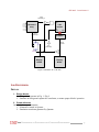
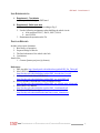
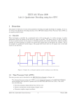
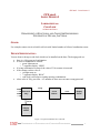
CPE 100L LOGIC DESIGN I CPE 100L LOGIC DESIGN I LABORATORY 11: CODE LOCK BY GRZEGORZ CHMAJ DEPARTMENT OF ELECTRICAL AND COMPUTER ENGINEERING UNIVERSITY OF NEVADA, LAS VEGAS GOALS: Use a simple counter circuit to build code lock with limited number of allowed combination errors. DESIGN SPECIFICATION: You are about to design a code lock which is to be installed on the door. The design goals are: there is a 4-bit password combination if correct combination is entered: o green light turns on o 7-segments display ‘OPEN’ if wrong combination is entered, the value of 3-bit counter is increased if the counter reaches value R: o red light turns on o 7-segments display ‘BLOC’ o code lock is no longer accepting entering combinations select value of R by your own – it is number of times user can enter wrong password wrong Password entry count failures block Display ‘BLOC’ correct Display ‘OPEN’ Figure 1. Top level schematic for a code lock DEPARTMENT OF ELECTRICAL AND COMPUTER ENGINEERING 1 CPE 100L LOGIC DESIGN I Design blocks separately: Password entry: four bits of input 1 bit of output: o 0: wrong combination o 1: correct combination 3-bit counter: input: enable: 1-bit o 1: counter increases at clock cycle o 0: counter does not change its value at clock cycle input: enter: 1-bit o clock input, where ‘1’ or raising edge activates the counter output: 1-bit o 1: counter reached R o 0: counter did not reach R Note that counter module has to contain the gate circuitry which detects if R was reached. There is no need to output the number stored in the counter. Display ‘OPEN’: no need to use decoder wire pins directly to ‘0’ or ‘1’ use AND gate to enable or disable the whole block input: activate: when ‘1’ is provided to this input, then the whole block is activated and ‘OPEN’ lights up Display ‘BLOC’: no need to use decoder wire pins directly to ‘0’ or ‘1’ use AND gate to enable or disable the whole block input: activate: when ‘1’ is provided to this input, then the whole block is activated and ‘OPEN’ lights up DEPARTMENT OF ELECTRICAL AND COMPUTER ENGINEERING 2 CPE 100L LOGIC DESIGN I wrong activated by ‘0’ enable Password entry 3-bit counter enter (clock) correct (activated by ‘1’ output R detect max R exceeded enter (pushbutton) Display ‘OPEN’ Display ‘BLOC’ Figure 2. Schematic for a code lock LAB DELIVERIES: PRELAB: 1. Design blocks: 1. Design blocks present in Fig. 1 / Fig. 2 2. Simulate our design and capture the waveforms, to ensure proper blocks’ operation 2. Prelab deliveries Include in the report document: 1. Schematics created in Quartus 2. Simulation waveform generated by Quartus DEPARTMENT OF ELECTRICAL AND COMPUTER ENGINEERING 3 CPE 100L LOGIC DESIGN I LAB EXPERIMENTS: 1. Experiment 1: Test blocks 1. Test your blocks design on DE2 board 2. Experiment 2: Bulid code lock 1. Connect blocks into the circuit according to Fig. 2 2. Use the following assignments when building the whole circuit: a. 4-bit password: SW17, SW16, SW15, SW14 b. enter: KEY0 3. Demonstrate the operation to the TA. POSTLAB REPORT: Include in the report document: 1. Brief theory of operation 2. Proposed design of blocks 3. The final schematic of the whole code lock 4. Conclusions Attach files: 1. Counter Quartus projects (zip format) References: 1. DE2 pin table: http://faculty.unlv.edu/eelabs/docs/guides/DE2_Pin_Table.pdf 2. Altera DE2 Introduction http://faculty.unlv.edu/eelabs/docs/guides/DE2_Introduction_box.pdf 3. Getting started with Altera DE2 Board: http://faculty.unlv.edu/eelabs/docs/guides/DE2_tut_initialDE2.pdf 4. Altera: Quartus II Introduction Using Schematic Design http://faculty.unlv.edu/eelabs/docs/guides/DE2_tut_quartus_intro_schem.pdf 5. Altera DE2 User Manual http://faculty.unlv.edu/eelabs/docs/guides/DE2_UserManuall.pdf 6. Datasheets of 7400 series chips: http://faculty.unlv.edu/eelabs/index.html?navi=main_icdatasheets DEPARTMENT OF ELECTRICAL AND COMPUTER ENGINEERING 4