1
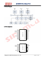
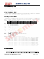
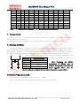
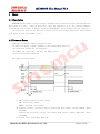
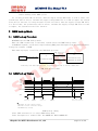
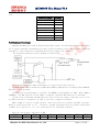
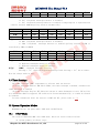
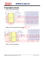
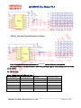
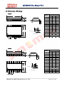
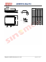
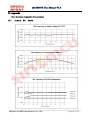
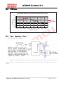
MC10P01B User Manual V1.4 8 Bit MCU designed by SinoMCU 2013/01/17 Note: Should there be any inconsistencies between Chinese and English version, the Chinese version shall prevail. 上海晟矽微电子有限公司 Shanghai SinoMCU Microelectronics Co., Ltd. MC10P01B User Manual V1.4 Contents 1 2 3 4 5 6 7 8 9 10 11 12 13 14 15 Description ....................................................................... 4 1.1 Product Features ............................................................ 4 1.2 Block Diagram ............................................................... 5 1.3 Pin Assignment .............................................................. 5 1.4 Pin Description ............................................................. 6 CPU ............................................................................... 6 2.1 Instruction Set ............................................................. 6 2.2 Address Space ............................................................... 6 2.3 Program Memory - ROM ........................................................ 7 2.4 User Data Memory - RAM ...................................................... 7 2.5 Configuration Bit - OPBIT ................................................... 7 2.6 Control Registers ........................................................... 7 System Clock ...................................................................... 8 3.1 External Oscillator ......................................................... 8 3.2 Internal High-accuracy RC ................................................... 8 Reset ............................................................................. 9 4.1 Description ................................................................. 9 4.2 Power-on Reset .............................................................. 9 RAM back-up Mode ................................................................. 10 5.1 RAM back-up Flow chart ..................................................... 10 5.2 RAM back-up Timing ......................................................... 10 GPIO ............................................................................. 11 Timer ............................................................................ 13 IROUT Port ...................................................................... 15 Interrupt ........................................................................ 16 9.1 General Description ........................................................ 16 9.2 Keyboard Interrupt ......................................................... 17 9.3 Timer Interrupt ............................................................ 18 System Operation Modes ......................................................... 18 10.1 STOP Mode ................................................................ 18 10.2 WAIT Mode ................................................................ 19 Electrical Specification ....................................................... 20 11.1 Absolute Maximum Rating................................................... 20 11.2 DC Electrical Characteristics............................................. 20 11.3 AC Electrical Characteristics............................................. 21 Typical Application Schematics.................................................. 22 Mode List ...................................................................... 23 Dimension of Package ........................................................... 24 Appendix ....................................................................... 26 15.1 Internal RC Curve ...................................................... 26 15.2 POR Curve ................................................................ 27 15.3 Input Impedance Curve................................................... 27 Shanghai SinoMCU Microelectronics Co., Ltd. page 2 of 29 MC10P01B User Manual V1.4 16 15.4 Port Schmitt(SMIT ) VIH VIL Curve...................................... 28 REVISION HISTORY ............................................................... 29 Shanghai SinoMCU Microelectronics Co., Ltd. page 3 of 29 MC10P01B User Manual V1.4 MC10P01B User Manual V1.4 1 Description MC10P01B is a high-performance, 8-bit Microcontroller. It has internal high-accuracy RC oscillator circuit and infrared emission diode driving circuit. It provides perfect solution for the remote control of TV, DVD, STB etc. 1.1 Product Features 8-bit CPU with CISC structure (compatible with HC05) 1K*8 bits OTP ROM 32 bytes RAM (including stack) 8-bit timer 9 channels keyboard interrupt (KBI) Infrared remote control code output IROUT, which has 8 types carrier frequency selectable, and can drive infrared emission diode directly Two types of oscillating mode: External crystal or ceramic oscillator with frequency from 325KHz to 8MHz Internal high-accuracy 4MHz RC oscillator (Frequency deviation less than 1%; CONDITION: 3.0V, 25 ℃) Low power dissipation (STOP model current less than 1uA@3V) RAM back-up function (CONDITION: supply voltage is higher than 1.1V) Serial programming interface circuit Protecting program memory data Operating voltage range 2.0~5.5V @ External oscillating mode 1.8~5.5V @ Internal oscillating mode Package type: SOP20 (300mil), SOP16 (150mil) TSSOP20(173mil) Shanghai SinoMCU Microelectronics Co., Ltd. page 4 of 29 MC10P01B User Manual V1.4 1.2 Block Diagram 1.3 Pin Assignment 1 2 3 4 PA1 PA2 VPP/PB0 5 6 7 PA3 8 PA4 9 12 PA5 10 11 MC10P01B0M GND OSCI/PC0 OSCO/PC1 PA0 20 19 18 17 VDD IROUT PB7 PB6 16 15 14 PB5 PB4 PB3 PB2 13 PA7 PA6 SOP20(300mil) 1 2 3 4 PA1 PA2 VPP/PB0 5 6 7 PA3 8 MC10P01B0K GND OSCI/PC0 OSCO/PC1 PA0 16 15 14 13 VDD IROUT PB7 PB6 12 11 10 PB5 PB4 PB3 PA7 9 SOP16(150mil) Shanghai SinoMCU Microelectronics Co., Ltd. page 5 of 29 MC10P01B User Manual V1.4 1 2 3 4 PA1 PA2 VPP/PB0 5 6 7 MC10P01B0Y GND OSCI/PC0 OSCO/PC1 PA0 20 19 18 17 VDD IROUT PB7 PB6 16 15 14 PB5 PB4 PB3 PB2 PA3 8 PA4 9 12 13 PA5 10 11 PA7 PA6 TSSOP20(173mil) 1.4 Pin Description Name Direction Function Description OSCI/PC0 I/O External Oscillator/GPIO (while configured as internal RC mode) OSCO/PC1 I/O External Oscillator/GPIO (while configured as internal RC mode) GND P Ground VDD P Source VPP/PB0 I Programming high voltage input; Input only, pull-up resistor selectable, keyboard interrupt can be triggered PB2-PB7 I/O GPIO,pull-up resistor selectable PA0-PA7 I/O GPIO, keyboard interrupt can be triggered, pull-up resistor is enable when trigger mode 2 CPU 2.1 Instruction Set MC10P01B uses HC05 compatible instruction set. For detail information about instruction set, please refer to the datasheet “HC05 Instruction Set” provided by SinoMCU. 2.2 Address Space $0000-$000F:Control Register $0010-$00DF:Reserved $00E0-$00FF:RAM(including Stack) $0100-$1BFF:Reserved $1C00-$1FFF:OTP ROM Shanghai SinoMCU Microelectronics Co., Ltd. page 6 of 29 MC10P01B User Manual V1.4 2.3 Program Memory - ROM Program memory of MC10P01B, which is used to store instructions, is an OTP ROM with size of 1K bytes. The highest address ($1FF0~$1FFF) area of program memory is reset/interrupt vector area , Refer to (§8.1). 2.4 User Data Memory - RAM User data memory of MC10P01B has 32 bytes, which are shared with stack. For more information about stack, please refer to the datasheet “HC05 Instruction Set”. 2.5 Configuration Bit - OPBIT Configuration Bit (OPBIT) is a special bit of OTP. It is used as configuring system functions. OPBIT is set while programming OTP ROM data with special programmer designed by SinoMCU. MC10P01B’s OPBIT is defined as follows. Bit 7 Bit 6 Bit 5 Bit 4 Bit 3 Bit 2 Bit 1 Bit 0 OPBIT ENCR PBP0 IRPO RCEN FC2 FC1 FC0 BIT[7] ENCR – Program memory protection bit 0:Protection is enabled 1:Protection is disabled BIT[5] PBP0 – PB0 pull-up enable bit 0:PB0 100Kohm pull-up resistor is disabled 1:PB0 100Kohm pull-up resistor is enabled BIT[4] IRPO – IROUT logic selection 0:IROUT outputs negative logic 1:IROUT outputs positive logic BIT[3] RCEN – Internal RC / External OSC selection 0:External OSC mode 1:Internal RC mode BIT[2:0] FC[2:0] – Carrier wave frequency selection 000:Carrier frequency is 1/6 of system frequency (about 38KHz @ Fosc=455KHz) 001:Carrier frequency is 1/36 of system frequency (about 56KHz @ Fosc=4MHz) 010:Carrier frequency is 1/50 of system frequency (about 40KHz @ Fosc=4MHz) 011:Carrier frequency is 1/53 of system frequency (about 38KHz @ Fosc=4MHz) 100:Carrier frequency is 1/56 of system frequency (about 36KHz @ Fosc=4MHz) 101:Carrier frequency is 1/61 of system frequency (about 33KHz @ Fosc=4MHz) 110:Carrier frequency is 1/64 of system frequency (about 31.5KHz @ Fosc=4MHz) 111:Carrier frequency is 1/74 of system frequency (about 27KHz @ Fosc=4MHz) 2.6 Control Registers All the registers of MC10P01B are listed below. Detail functions of these registers are described in the following contents. Address Name R/W Bit 7 Bit 6 Bit 5 Shanghai SinoMCU Microelectronics Co., Ltd. Bit 4 Bit 3 Bit 2 Bit 1 Bit 0 初始值 page 7 of 29 MC10P01B User Manual V1.4 $00 PA R/W PA7 PA6 PA5 PA4 PA3 PA2 PA1 PA0 0000 0000 $01 PB R/W PB7 PB6 PB5 PB4 PB3 PB2 - PB0 0000 00-0 $04 DDRA R/W DDRA7 DDRA6 DDRA5 DDRA4 DDRA3 DDRA2 DDRA1 DDRA0 0000 0000 $05 DDRB R/W DDRB7 DDRB6 DDRB5 DDRB4 DDRB3 DDRB2 $08 TDR R/W R/W TDR7 TDR6 TDR5 TDR4 TDR3 TDR2 TDR1 KBEB0 0000 00-0 TDR0 uuuu uuuu $09 TCR TIF TIM - - PRER PR2 PR1 PR0 01-- 0100 $0B KBIM R/W KBE7 KBE6 KBE5 KBE4 KBE3 KBE2 KBE1 KBE0 0000 0000 $0C MCR R/W KBIE KBIC - PBP PBP3 PBP2 OUTC FCAE 00-0 0000 R/W - - - - - - PC1 PC0 ---- --00 DDRC R/W - - - - - - $0D $0E PC DDRC1 DDRC0 ---- --00 Note: “-” means the bit is not defined; “u” means the initial value is indefinite. 3 System Clock The signal Fosc is generated by external crystal (or ceramic) oscillator or internal high-accuracy RC oscillator. The primary system clock (Fsys) is 1/2 frequency division of the signal Fosc. 3.1 External Oscillator Crystal (or ceramic) oscillator is connected as following diagram when the external oscillator mode is selected. The oscillating frequency must be in the range of 325KHz to 8MHz. The capacitor Cx is usually required. It is strongly recommended to make the crystal (or ceramic) oscillator as near as possible to OSCI and OSCO pin, because of oscillating starting and stability. The following table lists some typical oscillator frequency and recommended capacitance value of Osc. Freq. Capacitance of Cx Cx. 8MHz 15p Cx Cx Note: Considering the different characteristics of different types of oscillator, the capacitance value listed are 455KHz 220p/470p merely suggested. Please select the capacitor cautiously according to the characteristic of crystal (or ceramic) oscillator. 4MHz 3.64MHz 15p/30p 15p/30p 3.2 Internal High-accuracy RC The frequency of MC10P01B’s RC oscillator is 4MHz. While selecting internal RC mode, PC0 and PC1 can be used as GPIO. Shanghai SinoMCU Microelectronics Co., Ltd. page 8 of 29 MC10P01B User Manual V1.4 4 Reset 4.1 Description MC10PO1B has the power-on reset circuit, though without external reset pin. System will reset when power-on occurs. Power-on reset will cause the program to go to the starting address, specified by the contents of memory locations $1FFE:$1FFF, and initialize all the register. The oscillator stops for the duration of reset. To wait oscillating stabilized, the processor will begin to work after 4096 cycles. 4.2 Power-on Reset Following is the procedure of power-on reset: (1) Wait for supply voltage climbing up and stabilizing above VPOR. (2) Initialize PC and all the registers. (3) Enable the oscillator, and wait for 4096 cycles. (4) Processor starts execution. The power-on reset timing: ① POR: Internal power-on reset signal OSC: Oscillating signal RESET: Internal reset signal ② External crystal oscillator starts oscillating when supply voltage VDD>2V, while Tsu>50ms Internal RC oscillator starts oscillating when supply voltage VDD>1.55V, while Tsu>100ms ③ System reset occurs when VDD<1.5V. Shanghai SinoMCU Microelectronics Co., Ltd. page 9 of 29 MC10P01B User Manual V1.4 When VDD>1.55V , the oscillation circuit is active and system reset is released, system starts working after 4096 cycles. So, if using internal RC oscillator, when the supply voltage VDD falls to 1.5V or lower, the system reset will be active, and when the supply voltage VDD rises to 1.55V or higher, the system reset will be inactive. If using external crystal oscillator, when the supply voltage VDD falls to 1.5V or lower, the system reset will be active, and when the supply voltage VDD rises to 2.0V or higher, the system reset will be inactive. 5 RAM back-up Mode 5.1 RAM back-up Flow chart MC10P01B has the RAM back-up mode. When the STOP instruction is executed, system enters the RAM back-up state. At RAM back-up mode, oscillation stops retaining RAM, power dissipation can be reduced without losing the contents of RAM. When wake-up input, it will be exit RAM back-up state. STOP instruction is executed Reset B A (Stabilizing time) Oscillation work Wake up input Stabilizing time Oscillation stop (RAM back-up mode) Stabilizing time: Microcomputer starts its operation after FOSC is counted to 4096 times RAM back-up flow chart 5.2 RAM back-up Timing VDD 1.55V 1.5V 1.1V GND RAM DATA OLD DATA OLD DATA OLD DATA UNDEFINED DATA NEW DATA STOP STOP instruction POR RESET STOP instruction POR RESET Write RAM STOP instruction instruction ❶ 1.55V:Power on reset release voltage 1.5V:Power on reset occurrence voltage 1.1V:RAM back up voltage RAM back-up timing After STOP instruction,it enters RAM backup mode. Power dissipation is reduced (TYP. 0.1uA@VDD=3V, MAX.1uA@VDD=3V). Shanghai SinoMCU Microelectronics Co., Ltd. page 10 of 29 MC10P01B User Manual V1.4 When VDD drops down 1.5V, power on reset occurrence, MC10P01B reset and exit STOP state, all IO is in input mode, RAM’s data remaining. Now power dissipation is uncertain and may be small or large. When VDD drops down 1.1V, MC10P01B exit RAM back-up mode and RAM’s data maybe undefined. 6 GPIO MC10P01B has 16 general purpose input/output (GPIO) ports (PA7-PA0, PB7-PB2, PC1, PC0) and one input port (PB0). Each GPIO is controlled by the corresponding Data Register bit (PA, PB and PC) and Direction Register bit (DDRA, DDRB and DDRC). When a GPIO (excluding PC1 and PC0) is used as input port, it can select internal pull-up 100Kohm resistor or not through setting the register KBIM or PBP, PBP3 and PBP2 in MCR. The following figure shows the structure of GPIO. The function of data register and direction register is listed below. R/W DDR Function W 0 The port is in input mode. Data is written into the output data latch. W 1 The port is in output mode. Data is written into the output latch and output to the port. R 0 The port is in input mode. The state of port is read. R 1 The port is in output mode. The output data latch is read. Pas can be used as keyboard interrupt input. Each Pas can be configured by corresponding bit of KBIM. When KBEn=1 (n=0 to 7), Pan is configured as keyboard interrupt input, meanwhile the 100KΩ pull-up resistor is enable. For detail information about keyboard interrupt, please refer to §9.2. When PB2-PB7 is configured as input, internal pull-up resistor can be selected. The pull-up of PB2 is controlled by PBP2 in MCR, PB3’s is controlled by PBP3 in MRC, and PB4-PB7’s are all controlled by PBP. PB0 is used as high voltage input when programming OTP. Normally, it is used as an input, and has a selectable internal pull-up resistor, and can be configured as keyboard interrupt input (controlled by KBEB0 in DDRB). Refer to §9.2. PC1 and PC0 can be used as GPIO when internal RC mode is selected. Here are the relative registers of GPIO. Shanghai SinoMCU Microelectronics Co., Ltd. page 11 of 29 MC10P01B User Manual V1.4 $00 PA R/W Initial Value BIT[7:0] Pan Bit 7 Bit 6 Bit 5 Bit 4 PA7 PA6 PA5 PA4 R/W R/W R/W R/W 0 0 0 0 – PA Data register(n=7-0) Bit 3 PA3 R/W 0 $04 Bit 7 Bit 6 Bit 5 Bit 4 Bit 3 DDRA DDRA7 DDRA6 DDRA5 DDRA4 DDRA3 R/W R/W R/W R/W R/W R/W Initial Value 0 0 0 0 0 BIT[7:0] DDRAn – PA Direction register(n=7-0) 0:Configured to input 1:Configured to output Bit 2 PA2 R/W 0 Bit 1 PA1 R/W 0 Bit 0 PA0 R/W 0 Bit 2 DDRA2 R/W 0 Bit 1 DDRA1 R/W 0 Bit 0 DDRA0 R/W 0 Bit 1 - Bit 0 PB0 R 0 $01 Bit 7 Bit 6 Bit 5 Bit 4 Bit 3 PB PB7 PB6 PB5 PB4 PB3 R/W R/W R/W R/W R/W R/W Initial Value 0 0 0 0 0 BIT[7:2] PBn – PB Data register(n=7-2) BIT[0] PB0 – PB0 Data bit,it is read-only bit because PB0 $05 Bit 7 Bit 6 Bit 5 Bit 4 Bit 3 DDRB DDRB7 DDRB6 DDRB5 DDRB4 DDRB3 R/W R/W R/W R/W R/W R/W Initial Value 0 0 0 0 0 BIT[7:2] DDRBn – PB Direction register(n=7-2) 0:Configured to input 1:Configured to output Bit 2 PB2 R/W 0 is always input Bit 2 DDRB2 R/W 0 Bit 1 - Bit 0 KBEB0 R/W 0 $0C Bit 7 Bit 6 Bit 5 Bit 4 Bit 3 Bit 2 Bit 1 Bit 0 MCR KBIE KBIC PBP PBP3 PBP2 OUTC FCAE R/W R/W R/W R/W R/W R/W R/W R/W Initial Value 0 0 0 0 0 0 0 BIT[4] PBP – PB7-PB4 pull-up selection 0:PB7-PB4’s 100Kohm pull-up is disconnected 1:PB7-PB4’s 100Kohm pull-up is connected(the port must be configured to input) BIT[3] PBP3 – PB3 pull-up resistor set 0:PB3’s 100Kohm pull-up is disconnected 1:PB3’s 100Kohm pull-up is connected(the port must be configured to input) BIT[2] PBP2 – PB2 pull-up resistor set 0:PB2’s 100Kohm pull-up is disconnected 1:PB2’s 100Kohm pull-up is connected(the port must be configured to input) Note: PB0’s pull-up resistor is controlled by PBP0 in OPBIT. $0D Bit 7 Bit 6 Bit 5 Shanghai SinoMCU Microelectronics Co., Ltd. Bit 4 Bit 3 Bit 2 Bit 1 Bit 0 page 12 of 29 MC10P01B User Manual V1.4 PC R/W Initial Value BIT[1:0] PCn – PC Data $0E Bit 7 DDRC R/W Initial Value BIT[1:0] DDRCn – PC 0:Configured 1:Configured register(n=1-0) - Bit 6 Bit 5 Bit 4 Direction register(n=1-0) to input to output - - PC1 R/W 0 PC0 R/W 0 Bit 3 - Bit 2 - Bit 1 DDRC1 R/W 0 Bit 0 DDRC0 R/W 0 7 Timer The timer of MC10P01B contains a single 8-bit software programmable count-down counter with 7-bit software selectable prescaler. The counter may be preset under software control and decrements towards zero. When the counter decrements to zero, the timer interrupt flag (TIF bit in TCR) is set. Once the timer interrupt flag is set, an interrupt is generated to CPU only if TIM bit in TCR and I-bit in CCR are cleared. For more information about interrupt, please refer to §8.3. The timer counts the system clock (through prescaler) continuously. The contents of the counter (TDR) may be read at any time without disturbing the count. If writing TDR, the counter will count from the new value. The prescaler is a 7-bit divider, which can get division ratio of 1, 2, 4, 8, 16, 32, 64 or 128. PR2, PR2、PR1 and PR0 of TCR are programmed to choose the appropriate prescaler output which is used as the 8-bit counter clock input. The processor cannot write into or read from the prescaler; however, its contents can be cleared to all zeros by writing the PRER in the TCR. The timer block diagram is shown below. Shanghai SinoMCU Microelectronics Co., Ltd. page 13 of 29 MC10P01B User Manual V1.4 Here are the relative registers of Timer. $08 Bit 7 Bit 6 Bit 5 Bit 4 Bit 3 Bit 2 Bit 1 Bit 0 TDR TDR7 TDR6 TDR5 TDR4 TDR3 TDR2 TDR1 TDR0 R/W R/W R/W R/W R/W R/W R/W R/W R/W Initial Value u u u u u u u u BIT[7:0] TDR[7:0] – TDR is a read/write register which contains the current value of 8-bit count-down timer. $09 Bit 7 Bit 6 Bit 5 Bit 4 Bit 3 Bit 2 Bit 1 Bit 0 TCR TIF TIM PRER PR2 PR1 PR0 R/W R/W R/W R/W R/W R/W R/W Initial Value 0 1 0 1 0 0 BIT[7] TIF – Timer interrupt flag 0:The timer has not reached a count of zero 1:The timer has reached a count of zero Writing a “0”clears TIF. Writing a “1” has no effect. BIT[6] TIM – Timer interrupt mask 0:Timer interrupt is not masked (enabled). 1:Timer interrupt is masked (disabled). BIT[3] PRER –Prescaler reset bit Writing a “1” to PRER will reset prescaler to zero. This bit always reads as zero. BIT[2:0] PR[2:0] – Prescaler division ratio selection The following table lists the value of PR[2:0] and the corresponding division ratio. PR2 PR1 PR0 Division Ratio 0 0 0 1 Shanghai SinoMCU Microelectronics Co., Ltd. page 14 of 29 MC10P01B User Manual V1.4 8 IROUT 0 0 1 2 0 1 0 4 0 1 1 8 1 0 0 16 1 0 1 32 1 1 0 64 1 1 1 128 Port IROUT has ability to sink large current. It can drive infrared emission diode directly. IROUT outputs remote control signal with carrier wave whose duty ratio is 1/3. The frequency of IROUT has 8 types of selection controlled by FC[2:0] in OPBIT. IRPO of OPBIT controls positive or negative logic of IROUT signal. The IROUT control logic is shown below. FCAE and OUTC in MCR controls whether carrier wave is valid or not. IRPO in MCR controls the logic of IROUT. If FCAE or OUTC is zero, the prescaler will be cleared to zero, which guaranteed the first cycle of IROUT is entire. The following is the truth table of IRPO, OUTC, FCAE and IROUT. IRPO FCAE OUTC IROUT 0 0 0 High-impedance 0 0 1 L(without carrier) 0 1 0 High-impedance 0 1 1 L(with carrier) 1 0 0 L 1 0 1 High-impedance 1 1 0 L 1 1 1 High-impedance(with carrier) The carrier wave of IROUT is generated based on the system clock (1/2 frequency of oscillator frequency). FC[2:0] in OPBIT[2:0] is used to configure the ratio as the following table. Shanghai SinoMCU Microelectronics Co., Ltd. page 15 of 29 MC10P01B User Manual V1.4 FC[2:0] Ratio to Fsys OSC. Frequency (Hz) 000 6 455K 37.91K 001 36 4M 55.56K 010 50 4M 40.00K 011 53 4M 37.74K 100 56 4M 35.71K 101 61 4M 32.78K 110 64 4M 31.25K 111 74 4M 27.03K Here are the relative registers of IROUT. $0C Bit 7 Bit 6 Bit 5 Bit 4 MCR KBIE KBIC PBP R/W R/W R/W R/W Initial Value 0 0 0 BIT[1] OUTC –IROUT logic control bit 0:IROUT outputs logic 0 1:IROUT outputs logic 1 BIT[0] FCAE – Carrier wave output enable bit 0:IROUT outputs without carrier wave 1:IROUT outputs with carrier wave IROUT Carrier Frequency (Hz) Bit 3 PBP3 R/W 0 Bit 2 PBP2 R/W 0 Bit 1 OUTC R/W 0 Bit 0 FCAE R/W 0 9 Interrupt 9.1 General Description The interrupts of MC10P01B are keyboard interrupt (KBI), timer interrupt (TMI) and software interrupt (SWI). KBI and TMI can be masked by I bit, which is in CPU status control register CCR, but SWI cannot be masked. Furthermore, SWI is also an instruct. For details about SWI, please refer to the data sheet “HC05 Instruction Set”. The process of interrupt response is: While interrupt request occurring, CPU pushes all the relative registers (5 bytes altogether) to the system stack, set I bit to 1, and mask all the other interrupts. Differently from system reset, hardware interrupt does not terminate current instruction execution, but suspends itself until current instruction finished. While responding interrupt, firstly, CPU fetches the entrance address of the interrupt service subroutine from the corresponding interrupt vector, then jumps to the subroutine and executes. Each interrupts service subroutine needs an RTI instruct. When executing RTI, CPU pops all status registers from the system stack, and executes the instruct exactly after the interrupt happened. Shanghai SinoMCU Microelectronics Co., Ltd. page 16 of 29 MC10P01B User Manual V1.4 The interrupt vectors are shown bellow. The priority is decreased from bottom to top in the list. INT Vector Address Interrupt $1FF0:$1FF1 Reserved $1FF2:$1FF3 Reserved $1FF4:$1FF5 KBI $1FF6:$1FF7 TMI $1FF8:$1FF9 Reserved $1FFA:$1FFB Reserved $1FFC:$1FFD SWI $1FFE:$1FFF RESET 9.2 Keyboard Interrupt PA0-PA7 and PB0 can be used as keyboard interrupt inputs. All the keyboard interrupt inputs use a single interrupt requirement port and a single interrupt vector. The processor must read from GPIO’s data register to determine which port triggers the interrupt. The keyboard interrupt circuit diagram is shown below. The keyboard interrupt (KBI) requirement is relative with three factors. (1) KBIE in MCR. KBIE is enable bit of KBI. While KBIE=1, KBI function is enabled. While KBIE=0, KBI function is disabled. (2) KBE[7:0] (corresponding to PA[7:0]) and KBEB0 (corresponding to PB0). While KBEn=1 (KBEB0=1), the KBI function of Pan (PB0) is enabled, otherwise KBI function is disabled. (3) The state of PA7-PA0 and PB0. When the state of the pin changes from high level to low, the KBI interrupt is triggered. So, KBI is low level triggered interrupt. KBIC in MCR is relative to KBI response. After the processor responds the KBIC interrupt, KBIC bit should be written to “1”, otherwise, the KBI requirement will be latched, which means if KBIC not be written to “1”,the interrupt will be responded endlessly. Here are the relative registers of KBI. $0B Bit 7 Bit 6 Bit 5 KBIM KBE7 KBE6 KBE5 Shanghai SinoMCU Microelectronics Co., Ltd. Bit 4 KBE4 Bit 3 KBE3 Bit 2 KBE2 Bit 1 KBE1 Bit 0 KBE0 page 17 of 29 MC10P01B User Manual V1.4 R/W R/W R/W R/W R/W R/W R/W R/W R/W Initial Value 0 0 0 0 0 0 0 0 BIT[7:0] KBEn – PA keyboard interrupt function enable bit(n=7-0) 0:Pan’s keyboard interrupt function is disabled 1:Pan’s keyboard interrupt function is enabled (configuring Pan to input mode and connects internal 100Kohm pull-up resistor automatically) $05 Bit 7 Bit 6 Bit 5 Bit 4 Bit 3 Bit 2 Bit 1 Bit 0 DDRB DDRB7 DDRB6 DDRB5 DDRB4 DDRB3 DDRB2 KBEB0 R/W R/W R/W R/W R/W R/W R/W R/W Initial Value 0 0 0 0 0 0 0 BIT[0] KBEB0 – PB0 keyboard interrupt function enable bit 0:PB0’s keyboard interrupt function is disabled 1 : PB0 ‘ s keyboard interrupt function is enabled (pull-up resistor of PB0 is controlled by PBP0 in OPBIT) $0C Bit 7 Bit 6 Bit 5 Bit 4 Bit 3 Bit 2 Bit 1 MCR KBIE KBIC PBP PBP3 PBP2 OUTC R/W R/W R/W R/W R/W R/W R/W Initial Value 0 0 0 0 0 0 BIT[7] KBIE – Keyboard interrupt enable bit 0:Keyboard interrupts master is disabled. 1:Keyboard interrupts master is enabled. BIT[6] KBIC – Keyboard interrupt clear bit Writing a “1” clears the keyboard interrupt latch. Writing a “0” has no This bit always reads as zero. Bit 0 FCAE R/W 0 effect. 9.3 Timer Interrupt The timer interrupt (TMI) requirement is relative with two factors. (1) Timer interrupt mask bit TIM. While TIM=1, the timer interrupt is masked, otherwise the timer interrupt is enabled. (2) Timer interrupt flag bit TIF. When the counter of timer decrements to zero, TIF will be set, which means TMI is triggered. TIF could not be cleared automatically, so it must be cleared by software. For more information about the function of TMI and TIF, please refer to §6. 10 System Operation Modes MC10P01B has two low power modes: STOP mode and WAIT mode. 10.1 STOP Mode The instruct STOP makes MCU enter STOP mode, which has several effects bellow: System primary oscillator stops Shanghai SinoMCU Microelectronics Co., Ltd. page 18 of 29 MC10P01B User Manual V1.4 Clear I bit in CCR, and enable interrupt Data stored in RAM will be maintained All states of GPIO remain System primary oscillator stops All the internal operation stops If one of the following things happens, MCU will exit from STOP mode. KBI request occurs Any type of system reset occurs While MCU works under STOP mode, almost all the operations terminate, so the power dissipation is very low. 10.2 WAIT Mode The instruct WAIT makes MCU enter WAIT mode, which has several effects bellow: CPU clock stops CPU process and internal bus activities terminate Clear I bit in CCR, and enable interrupt Data stored in RAM will be maintained All states of GPIO remain All states of registers remain If one of the following things happens, CPU clock will restarts and MCU will exit from WAIT mode. Any type of interrupt request occur Any type of system reset occurs While MCU works under WAIT mode, activities of CPU stop, but the system primary oscillator still works, so the power dissipation is lower than under normal mode. Shanghai SinoMCU Microelectronics Co., Ltd. page 19 of 29 MC10P01B User Manual V1.4 11 Electrical Specification 11.1 11.2 Absolute Maximum Rating Parameter Symbol Ratings/Value Unit Supply Voltage VDD -0.3~6.5 V Input Voltage VIN VSS-0.3~VDD+0.3 V Operating Temperature TA -20~70 ℃ Storage Temperature Tstg -65~150 ℃ DC Electrical Characteristics (VDD=3V,T=25℃) Characteristics Symbol Pin Operating Voltage VDD RAM back-up Voltage VDD Input Leakage Current Vleak All input ports Input High Voltage Vih All input ports Input Low Voltage Vil Pull-up Resistance Pull-up Resistance Condition Min. Typ. Max. Unit External Oscillating 2.0 5.5 V Internal Oscillating 1.8 5.5 V 1.1 5.5 V ±1 uA 0.7VDD VDD V All input ports 0 0.3VDD V RU1 PA7-PA0 PB7-PB2 50 100 200 Kohm RU2 PB0 50 100 200 Kohm Ioh PA7-PA0 PB7-PB2 PC1-PC0 IROUT Voh=2.7V 3 5 mA Output Low Current Iol1 PA7-PA0 PB7-PB2 PC1-PC0 Vol=0.3V 10 14 mA Output Low Current Iol2 IROUT Vol=1.5V 300 400 mA Idle Supply Current Idds VDD VDD=3V in STOP mode Dynamic Supply Current Iddc VDD VDD=3V no load LVR Voltage Vlvr Output High Current Shanghai SinoMCU Microelectronics Co., Ltd. VIN=VDD,0 T=-20℃~70℃ 0.1 1.25 1.5 1 uA 3 mA 1.75 V page 20 of 29 MC10P01B User Manual V1.4 11.3 AC Electrical Characteristics VDD=3V,T=25℃ Characteristics Symbol External Oscillator Frequency Fosc Pin Condition Min. 325K Typ. Max. 8M Hz Fhrc1 T=25℃ VDD=3V -1% 4 +1% MHz Fhrc2 T=-20℃~70℃ VDD=1.8~3.6V -2% 4 +2% MHz Internal RC Frequency Shanghai SinoMCU Microelectronics Co., Ltd. page 21 of 29 MC10P01B User Manual V1.4 12 Typical Application Schematics SOP20,Internal RC Oscillator SOP20,External Crystal/Ceramic Oscillator SOP16,Internal RC Oscillator Shanghai SinoMCU Microelectronics Co., Ltd. page 22 of 29 MC10P01B User Manual V1.4 SOP16,External Crystal/Ceramic Oscillator Note1: If using RAM data remaining function, the electrolytic capacitor C2 should not be omitted. Note2: If the current of the infrared emission diode D1 is particularly large, the current-limiting resistor R1 should not be omitted. 13 Mode List Green Package Option(Pb/Halide-free ) IRC Speed(MHz) Ordering Code Package 4.000 MC10P01B0K SOP16 -20℃ to 70℃ 4.000 MC10P01B0M SOP20 -20℃ to 70℃ 4.000 MC10P01B0Y TSSOP20 -20℃ to 70℃ 4.030 MC10P01B1K SOP16 -20℃ to 70℃ 4.030 MC10P01B1M SOP20 -20℃ to 70℃ 4.030 MC10P01B1Y TSSOP20 -20℃ to 70℃ Shanghai SinoMCU Microelectronics Co., Ltd. Operation Range page 23 of 29 MC10P01B User Manual V1.4 14 Dimension of Package SOP20 SYMBOL D A3 A2 A c A1 L θ L1 b b1 E1 E c1 c BASE METAL WITH PLATING SECTION B-B MILLIMETER MIN NOM MAX A - - 2.70 A1 0.10 0.20 0.30 A2 2.10 2.30 2.50 A3 0.92 1.02 1.12 b 0.35 - 0.44 b1 0.34 0.37 0.39 c 0.26 - 0.31 c1 0.24 0.25 0.26 D 12.60 12.80 13.00 E 10.10 10.30 10.50 E1 7.30 7.50 7.70 e L 1.27BSC 0.70 0.85 L1 θ b e B 1.00 1.40BSC 0 - 8° B SOP16 D SYMBOL A3 A2 A c A1 L θ L1 b b1 E1 E BASE METAL c1 c MILLIMETER MIN NOM MAX A - - 1.77 A1 0.08 0.18 0.28 A2 1.20 1.40 1.60 A3 0.55 0.65 0.75 b 0.39 - 0.48 b1 0.38 0.41 0.43 c 0.21 - 0.26 c1 0.19 0.20 0.21 D 9.70 9.90 10.10 E 5.80 6.00 6.20 E1 3.70 3.90 4.10 e WITH PLATING SECTION B-B b e L 1.27BSC 0.50 L1 θ 0.65 0 - B B Shanghai SinoMCU Microelectronics Co., Ltd. 0.80 1.05BSC page 24 of 29 8° MC10P01B User Manual V1.4 TSSOP20 D SYMBOL A3 A2 A c A1 L θ L1 b b1 E1 E BASE METAL c1 c MILLIMETER MIN NOM MAX A - - 1.20 A1 0.05 - 0.15 A2 0.90 1.00 1.05 A3 0.34 0.44 0.54 b 0.20 - 0.28 b1 0.20 0.22 0.24 c 0.10 - 0.19 c1 0.10 0.13 0.15 D 6.40 6.50 6.60 E 6.20 6.40 6.60 E1 4.30 4.40 4.50 e WITH PLATING SECTION B-B L e 0.45 L1 θ b 0.65BSC 0.60 1.00BSC 0 - B B Shanghai SinoMCU Microelectronics Co., Ltd. 0.75 page 25 of 29 8° MC10P01B User Manual V1.4 15 Appendix Note : the contents of appendix is for your reference 15.1 Internal RC Curve Shanghai SinoMCU Microelectronics Co., Ltd. page 26 of 29 MC10P01B User Manual V1.4 15.2 POR Curve MC10P01B POR Cure For VDD With Temperature Change 1.8 Voltage(V) 1.7 1.6 POR up 1.5 POR down 1.4 1.3 1.2 -40℃ -30℃ -20℃ -10℃ -1℃ 25℃ 50℃ 70℃ 85℃ Temperature(℃) 15.3 Input Impedance Curve The test model as follows: Adjust r1 at different supply voltage, the r1 resistor value mark as VIH when PC1 output from L signal to H signal.And,the r1 resistor value mark as VIL when PC1 output H signal to L signal. Shanghai SinoMCU Microelectronics Co., Ltd. page 27 of 29 MC10P01B User Manual V1.4 15.4 Port Schmitt(SMIT ) VIH VIL Curve The test model as follows: Adjust r1 at defferent supply voltage, the voltmeter value mark as VIH when PC1 output from L signal to H signal.And,the voltmeter value mark as VIL when PC1 output H signal to L signal. Shanghai SinoMCU Microelectronics Co., Ltd. page 28 of 29 MC10P01B User Manual V1.4 16 REVISION HISTORY REV. Date Description 1.0 2012-3-28 First edition issued 1.1 2012-8-6 (1)§1.1 IROUT add open-drian description (2)§2.1 Delete the “MUL instruction unavailable ”section (3)§2.5、§4 Fix up resistor value to 100K (4)§3.1 Fix the capacitance description of external crystal circuit. (5)§9.2 Change the value of up-resistor, IOH, LVR 1.2 2012-11-20 (1)§6 IROUT output truth table (2)Add TSSOP20 package type 1.3 2013-01-07 (1)Add §4,§12,§14.2、§14.3 section 1.4 2013-01-17 (1)§1.1 RAM back-up function (2)Add §5, §5.1, §5.2 section (3)Add §11.2 RAM back-up Voltage Shanghai SinoMCU Microelectronics Co., Ltd. page 29 of 29