1
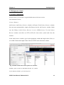
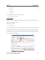
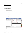
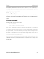
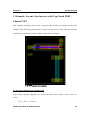
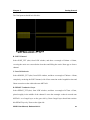
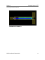
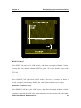
UNIVERSITY OF MINNESOTA OPDK User Manual Release 2011.3 Wei Zhang March 2011 OPDK User Manual, Release 2011.3, March 2011 Copyright © 2011 University of Minnesota. All rights reserved. Unpublished-rights reserved under the copyright laws of the United States. Use of copyright notices is precautionary and does not imply publication or disclosure. Contact VLSI Group @ University of Minnesota Contact VLSI Group @ University of Minnesota by: Telephone: (612) – 626 – 0834 Fax: (612)-626-4583 VLSI Group, ECE Department, University of Minnesota Keller Hall (EECS Building), 4-168 200 Union Street SE Minneapolis, MN 55455 Questions & Comments Contact author (Wei Zhang) by: Email: [email protected] OPDK User Manual, Release 2011.3 II Using This Manual This manual describes the Organic Process Design Kit (OPDK) and how to use it. Audience This manual is intended for designers who use OPDK to develop, test, analyze and modify organic circuit designs in ion-gel gated OTFT technique, and designers who develop device descriptions as an extension for other specific organic transistor structures. Related Documents The following documents pertain to this manual: OPDK Features OPDK Release Notes OPDK User Manual, Release 2011.3 III Conventions OPDK User Manual uses the following conventions, unless otherwise specified. Convention Description menuName -> commandName Indicates the name of the menu and the command name. For example, File -> Save as refers to the “Save as” command in the “File” menu. times italic Indicates commands, functions, arguments, file names and variables with a line of text. When a variable is included in italicized text, the variable is enclosed by angle brackets (<>). For example, “setenv OPDK_DIR/<your_absolute_local_ path>/OPDK”, where <your_absolute_local_path> is your absolute local path of your OPDK directory. <> Other Sources of Information The OPDK external website provides information for OPDK updates, downloads and documentation. The website can be accessed at http://opdk.umn.edu. Acknowledgement The author would like to thank: 1. NCSU-FreePDK45 Developer Team (North Carolina State University and Oklahoma State University) for providing software framework for OPDK development. NCSU-FreePDK45 Website: http://www.eda.ncsu.edu/wiki/FreePDK 2. National Science Foundation for funding support. 3. Dr. C. Daniel Frisbie’s group in Chemical Engineering and Materials Science Department at the University of Minnesota for technical support in organic electronics information. 4. Dr. Chris H. Kim’s group in Electrical and Computer Engineering Department at the University of Minnesota for technical support in software development and website design. OPDK User Manual, Release 2011.3 IV Table of Contents TABLE OF CONTENTS Chapter 1 – Introducing OPDK ----------------------------------------------------------------- 3 Introducing Organic Thin-Film-Transistor (OTFT) -------------------------------- 4 The Organic Process Design Kit (OPDK) – Definition and Purpose ------------- 7 The Organic Process Design Kit (OPDK) – Features ------------------------------ 8 Chapter 2 – Getting Started --------------------------------------------------------------------- 9 System Requirements -------------------------------------------------------------------- 10 Setup OPDK ----------------------------------------------------------------------------- 11 Example: Design of an Inverter with Top-Gated P3HT-Channel TFT ---------- 13 Example: Layout of an Inverter with Top-Gated P3HT-Channel TFT ---------- 20 Chapter 3 – Designing Layout of OTFT ------------------------------------------------------ 33 Supported OTFT Devices -------------------------------------------------------------- 34 Layout of the Ion-Gel-Top-Gated P3HT-Channel OTFT ------------------------- 35 Layout of the Ion-Gel-Top-Gated CNT-Channel OTFT --------------------------- 38 Chapter 4 – Designing Layout of Passive Devices ------------------------------------------- 42 Supported Passive Devices ------------------------------------------------------------- 43 Layout of Resistor ----------------------------------------------------------------------- 44 Layout of Capacitor ---------------------------------------------------------------------- 46 Chapter 5 – Applying Cross-Overs for Interconnections ------------------------------------- 49 Introducing Cross-Over ------------------------------------------------------------------ 50 Layout of Cross-Over -------------------------------------------------------------------- 51 Chapter 6 – Using P-Cells ------------------------------------------------------------------------- 53 Purpose of P-Cell ------------------------------------------------------------------------- 54 Supported Devices ------------------------------------------------------------------------ 55 Using P-Cell for Ion-Gel-Top-Gated P3HT-Channel OTFT ------------------------ 56 OPDK User Manual, Release 2011.3 1 Table of Contents Using P-Cell for Ion-Gel-Top-Gated CNT-Channel OTFT ------------------------- 58 Using P-Cell for Capacitor --------------------------------------------------------------- 60 Chapter 7 – Simulating Circuits ------------------------------------------------------------------- 62 Introducing Device Models -------------------------------------------------------------- 63 Simulating with HSPICE ----------------------------------------------------------------- 64 OPDK User Manual, Release 2011.3 2 Chapter 1 Introducing OPDK Chapter 1 Introducing OPDK This chapter introduces basic background of the Organic Process Design Kit (OPDK). Introducing Organic Thin-Film-Transistor (OTFT) The Organic Process Design Kit (OPDK) – Definition and Purpose The Organic Process Design Kit (OPDK) – Features OPDK User Manual, Release 2011.3 3 Chapter 1 Introducing OPDK Introducing Organic Thin-Film-Transistor (OTFT) The integration of electronics onto the flexible substrate, including plastic and metal foils, will greatly expand the application area of microelectronics. However, difficulties have been encountered with the traditional silicon transistors, mainly due to their rigid lattice structure and the high temperature during fabrication. Organic thin-film transistors [1], which are composed of polymers, have been demonstrated to be a potential solution. Furthermore, the feasibility of printing organic transistors also indicates the perspective of low-cost fabrication. Organic transistors, however, usually suffer from low carrier mobility, resulting in a high operation voltage. Few attempts have been made on printable, low-voltage organic transistors. Here we demonstrate a printable gel-OTFT technique which provides sufficient current under a low operation voltage (1V). A gel-OTFT is an organic thin-film transistor which is fabricated based on ion-gel, wherein ion-gel refers to an electrolyte formed by gelation of a triblock copolymer in an ionic liquid, acting as the gate dielectric. Figure 1.1 shows the basic structure and mechanism of a gel-OTFT and its current-voltage characteristics [1]. Poly(3-hexylthiophene) (P3HT) is printed between the two gold electrodes (source and drain) as the channel layer. An ion-gel layer covers the entire channel layer and a conducting polymer poly(3,4-ethylenedioxythiophene) : poly(styrenesulfonate) (PEDOT:PSS) is printed on the top as the gate electrode. When the gate is floating, the ions in the ion gel are randomly distributed and the entire gel displays a neutral state. When the gate is biased with a negative voltage, the ions are polarized by the electrical field and interfaces are formed near both surfaces of ion gel, creating two capacitors in serial. If a voltage difference is also applied between the source and the drain, carriers in the channel layer will start to flow, leading to a drain current. Since the distance between charges at each interface is quite small (at the order of nm), OPDK User Manual, Release 2011.3 4 Chapter 1 Introducing OPDK the equivalent gate capacitance is significantly high (~100 uF/cm2), which is around 70 times larger than that in the silicon transistors (~1.4 uF/cm2) [2]. Therefore, in spite of the relatively low carrier mobility, the large gate capacitance enables the transistor to generate a considerable current under a low operation voltage. V V D D = -0 .1 V = -1 .0 V The detailed current-voltage characteristic curve is shown in Figure 1.1(b). Under a low voltage (1V), a transistor with W/L = 500um/25um achieves 0.4mA drain current, which is sufficient in most applications. Another important aspect is the on/off ratio of the transistor, which is the ratio between drain currents under VGS = -1V and VGS = 0V. It can be noted that the on/off ratio is as high as 1000, which is good enough for digital applications. These data illustrate the feasibility of fabricating high-performance and stable low-voltage digital circuits with gel-OTFTs. The gel-OTFT demonstrated above is a p-type transistor with P3HT channel layer. N-type transistor is also possible in this technique if suitable N-type channel material is available. However, the introduction of a viable n-type material has been delayed due to unstable OPDK User Manual, Release 2011.3 5 Chapter 1 Introducing OPDK characteristics, no good contact, and significantly lower mobility than their p-type counterpart. Therefore, n-type device is not the focus of Organic Process Design Kit (OPDK) at the current stage. In conclusion, we have demonstrated our printable gel-OTFT technique, where the high gate capacitance caused by polarized ions is the key to generating significant current under a low operation voltage. The current-voltage characteristics have shown the great potential of gelOTFTs in achieving stable digital applications. References: [1] Y. Xia, W. Zhang, M. Ha, et al., “Printed Sub-2 V Gel-Electrolyte-Gated Polymer Transistors and Circuits”, Applied Functional Materials, Volume 20, Issue 4, pages 587–594, February 22, 2010. [2] W. Zhang, M. Ha, D. Braga, M. Renn, C.D. Frisbie, C.H. Kim, "A 1V Printed Organic DRAM Cell Based on Ion-Gel Gated Transistors with a Sub-10nW-per-Cell Refresh Power", International Solid-State Circuits Conference (ISSCC), February 2011 OPDK User Manual, Release 2011.3 6 Chapter 1 Introducing OPDK The Organic Process Design Kit (OPDK) – Definition and Purpose The main purpose of OPDK is to facilitate the entire OTFT circuit system design. The earlier OTFT designs rely on examinations by naked eyes and lack effective verification in either functionality or layout. To ensure reasonable yield for complex circuit systems, it is required to improve the design tools and introduce verification steps. Fortunately, sharing a lot in common with silicon transistors, especially in the structure, OTFTs are able to adapt similar techniques widely used in silicon industry. For example, among the mainstream computer-aided-design (CAD) software, Cadence Virtuoso© design environment is feasible to be utilized for OTFTs both for designing circuits and drawing layouts. Circuit simulation software such as HSPICE© is also an excellent candidate to verify the design functionality. The existing tools, however, cannot be directly utilized since the major characteristics and materials are totally different. Therefore, OPDK, the design kit specifically developed for OTFTs, targets at building a software package based on silicon transistors while following the real properties of OTFT. With the help of Cadence Virtuoso and HSPICE, it enables computer-based verifications on circuit and layout designs, and significantly reduces design load for large-scale systems. OPDK User Manual, Release 2011.3 7 Chapter 1 Introducing OPDK The Organic Process Design Kit (OPDK) – Features OPDK is a design kit developed for OTFT platform under the software environment of Cadence Virtuoso. It has the following major features: 1. Supports circuit design in Cadence environment; 2. Supports layout design in Cadence environment; 3. Supports major built-in tools in Cadence environment; 4. Supports circuit file generation through Cadence Virtuoso Analog Design Environment; 5. Supports design rule checks (DRC) for layouts; 6. Supports layout versus schematic (LVS) checks for layouts; 7. Supports all layers currently used in the OTFT platform, with other layers for future extension; 8. Supports two kinds of OTFT devices (ion-gel-top-gated OTFTs with P3HT or CNT channel layer); 9. Supports resistor with three unit resistance options; 10. Supports capacitor based on ion-gel-top-gated OTFT with P3HT channel layer; 11. Provides P-Cells for the two kinds of OTFT devices and for capacitor; 12. Provides HSPICE device models to perform functionality verification; 13. Provides examples of inverter, NAND, DFF, DRAM, etc. 14. Extensible for other types of organic devices, including N-type devices OPDK User Manual, Release 2011.3 8 Chapter 2 Getting Started Chapter 2 Getting Started This chapter provides the basic steps of using OPDK. For details, you may refer to Chapter 3-6. System Requirement Setup OPDK Example: Design of an Inverter with Top-Gated P3HT-Channel TFT Example: Layout of an Inverter with Top-Gated P3HT-Channel TFT OPDK User Manual, Release 2011.3 9 Chapter 2 Getting Started Before You Start – System Requirements To run all features Organic Process Design Kit (OPDK) in Cadence, please first make sure you have met the following system requirement: 1. Cadence Virtuoso, version 6.1.1 or higher. 2. Mentor Calibre 2006.4 (OA 2.2.5) or higher Running OPDK with a lower version of Cadence or Mentor is not tested and may require changes in configuration. If you are not sure about your system environment, please contact your IT support. OPDK User Manual, Release 2011.3 10 Chapter 2 Getting Started 1. Setup OPDK 1.1 Make a new directory called OPDK under your home directory: mkdir OPDK 1.2 Go to OPDK: cd OPDK 1.3 Copy the file OPDK-1.5.tar to directory OPDK by using the command from this directory: cp OPDK-1.5.tar.gz . 1.4 Extract the archive using the command tar -zxvf OPDK-1.5.tar.gz 1.5 You should now be able to see the extracted files under OPDK at your home directory. This contains an open-source, open-access based OPDK for organic electronic applications based on ion-gel technology from the Department of Chemical Engineering and Materials Science (CEMS) at the University of Minnesota, Twin Cities. 1.6 Go to organic_basekit/cdssetup under OPDK directory cd organic_basekit/cdssetup Here, you will have to modify setup.csh using vi, nano or any of your favorite editors as follows: 1.6.1 Comment out the line which defines the environment variable OPDK_DIR (it starts with "setenv”). Lines can be commented out by adding a # at the beginning. 1.6.2 Set the OPDK_DIR variable to the root directory of the OPDK distribution OPDK User Manual, Release 2011.3 11 Chapter 2 Getting Started setenv OPDK_DIR <your_absolute_local_path>/OPDK 1.6.3 Comment out the line which defines the environment variable CDSHOME. 1.6.4 Set the CDSHOME variable to the root directory the Cadence installation. For example: setenv CDSHOME /home/apps/common/cadence/Linux/ ic_611/tools.lnx86/ 1.6.5 Save and exit the file. Your OPDK is setup and ready to be used now. 1.7 Create your temporary Cadence work directory at OPDK cd OPDK/ mkdir cds cd cds Always run Cadence from this directory to avoid cluttering up your workspace. 1.8 Copy setup.csh (the file you modified in step 1.6) into this directory cp ../organic_basekit/cdssetup/setup.csh . Source this script using the following command source setup.csh This script copies the files needed by Cadence and initializes the environment. 1.9 Invoke Cadence by typing: virtuoso & This should bring up the command interface window and library manager. You are now ready to design circuits in Cadence. OPDK User Manual, Release 2011.3 12 Chapter 2 Getting Started 2. Example: Design of an Inverter with Top-Gated P3HTChannel TFT This example will help you familiarize yourself with OPDK in Cadence. This will show the most important commands and steps used when working with schematics in Cadence. As an example, you will design a simple inverter with resistor load. For details of the various components, please refer to the next few chapters. Before starting with the design example, there are a couple things worth mentioning: Most of the commands in Cadence can be accessed in multiple ways: pull-down menus, shortcut keys, buttons in toolbars, etc. In the described example, all the commands are referenced by their position in the pull-down menus. The shortcut keys can be found from the pull-down menus as well. The most frequently used key in Cadence is ESC. It is used to cancel on-going commands. The following picture shows the schematic of an inverter, which is ready for netlist extraction. The following section explains how to draw it in Cadence. OPDK User Manual, Release 2011.3 13 Chapter 2 Getting Started Fig. 2.2.1 Schematic of an inverter 2.1 Create a library for your new design From the library manager window: File->New->Library Type a new name, such as TEST, click OK. In the pop-up window, choose “Attach to an existing tech library”. Then, choose “OPDK_TechLib”). Click OK. 2.2 Create a new cell In the Library Manager, highlight your new library (TEST if that is what you chose). File->New->Cellview Choose library TEST, cell name “inverter”, view name “schematic”, and Open with “Schematic L”. Click OK. Click “Always” if “Upgrade License” warning message shows up. A schematic window will open. OPDK User Manual, Release 2011.3 14 Chapter 2 Getting Started 2.3 Design your circuit 2.3.1 Place components For this inverter, you will need a top-gated P3HT-channel TFT and a resistor. From Schematic window, Create->Instance Add Instance and Library Browser windows will open. If the Library Browser window does not open automatically, simply click Browse on the Add Instance window. Make sure the Library in the Library Browser is set to OPDK_Devices. Use the Library Browser window and click on PTFT_P3HT_TG, then select symbol and close the window. In the Add Instance window, type in the appropriate width and length values. Here we use width= 500um and length=50um. Place the PTFT in the schematic window. Fig. 2.2.2 Add a P3HT-OTFT device symbol into schematic Similarly, place a resistor of 10K Ohm with the “res” symbol. If you make any mistake, you can always use: OPDK User Manual, Release 2011.3 15 Chapter 2 Getting Started Edit->Delete or Edit->Rotate or Edit->Move or Edit->Stretch To change the properties of some of the components: Edit->Properties->Objects 2.3.2 Place pins For this inverter, you will need five pins: ground (GND), negative power (VDDN), input (IN), output (OUT) and substrate (SUB). From Schematic window, Create->Pin Add Pin window will open. Type in the pin names and place the pins in the appropriate locations. Pay attention to the red box shown below, and make sure you choose the right I/O direction for each pin. For example, IN should be Input, OUT should be Output, and all the rest should be InputOutput. OPDK User Manual, Release 2011.3 16 Chapter 2 Getting Started 2.3.3 Connect components Connect the component terminals as shown in the figure above using: Create->Wire (narrow) 2.4 Generate netlist files In the Schematic Window: Design->Check and Save There should be no errors. Then go Launch->ADE L. The window of Cadence Analog Design Environment will show up. Make sure the current simulator is set to hspiceD: Setup->Simulator/Directory/Host Set the simulator to hspiceD. Simulation->Netlist->Create Fig. 2.2.4 Create netlist from schematic view A new window will pop up showing the generated HSPICE netlist. You may save this file by clicking the menu bar: File->Save As OPDK User Manual, Release 2011.3 17 Chapter 2 Getting Started Specify the full path name and file name in the Save As window. If you have models ready, you can use this netlist file to run simulations with the model. You may need to modify some of the netlist, which we will not discuss in details. 2.5 Working with symbols If you want to use your design in other schematics, you need to create a symbol for it. This is equivalent to the use of sub-circuits in HSPICE. Using hierarchy in your project makes it easier to organize. 2.5.1 Create a new symbol Save the schematic before you create its symbol: File->Check and Save Create->Cellview->From Cellview, click OK. A new window will open with the symbol view. By default, the symbol shape is a rectangle, but you can change it. Since this design is an inverter, we will draw a triangle and put a small circle at the output. To do this, you will want to delete the green rectangle, draw the new shape, and move the terminals to new positions. Use Create->Shape to draw a triangle and place a circle. There are several shapes available: line, rectangle, circle, etc. You will also need to change the Selection box (the red rectangle), which defines the limits of the symbol. This can be done by stretching the Selection box. Figure below shows an example of the inverter symbol: OPDK User Manual, Release 2011.3 18 Chapter 2 Getting Started Fig. 2.2.5 Create symbol from schematic view Don't forget to check and save. 2.5.2 Use the symbol in other schematics Create a new schematic, using the instructions described in Create a new cell. Give a name such as test_inverter. You place this symbol in the new schematic in the same way that you placed any other components, with: Create->Instance This time change the Library to your library TEST and click on inverter. Your symbol should be here. To move in the hierarchy, select the inverter, and then: Edit->Hierarchy->Descend Edit. You can choose the schematic or the symbol for editing. To return to the previous schematic, use: Edit->Hierarchy->Return OPDK User Manual, Release 2011.3 19 Chapter 2 Getting Started 3. Example: Layout of an Inverter with Top-Gated P3HTChannel TFT This example will help you to create a layout for the inverter you designed in the first example. The following picture shows a layout for the inverter. The following sections explain how to make each of the separate components in Virtuoso. 3.1 Create a layout view of your cell In the Library Manager, Highlight your inverter schematic library (TEST if that is what you chose). File -> New -> Cellview OPDK User Manual, Release 2011.3 20 Chapter 2 Getting Started Change the view type to layout and open with layout L. Click OK. Click “Always” if there is any license upgrade message. A layout-editing and an LSW window will open up. 3.2 Layout the components for your circuit For this inverter we will need to layout a Top-gated P3HT-channel PTFT and a resistor. 3.2.1 Layout a PTFT For better illustration, it is recommended to draw different layers in the order of how it is actually fabricated. A. METAL1 In the LSW window, choose METAL1 (drw). From the Layout window, choose Create->Shape->Rectangle 1. Draw the source/drain electrodes. Assume we are going to draw a PTFT with W/L = 500um/50um, with a source/drain electrode width of 10um. Draw a rectangle of 500um x 10um, and draw another one under the first rectangle, with 50um distance in between. 2. Draw the source/drain connections to other nets. On the right side of the drawn electrodes, draw two rectangles in METAL1, each being 100um x 200um. 3. Draw the gate electrode. On the left side of the drawn electrodes, draw a rectangle of 100um x 200um in METAL1, with 100um distance away from the source/drain electrodes. OPDK User Manual, Release 2011.3 21 Chapter 2 Getting Started The final pattern should look like this: B. P3HT Channel Select P3HT_TFT (drw) from LSW window, and draw a rectangle of 500um x 120um, covering the entire two source/drain electrodes and filling the entire 50um gap to form a channel. C. Ion-Gel Dielectric Select IONGEL_TFT (drw) from LSW window, and draw a rectangle of 700um x 120um, completely enclosing the P3HT channel, with 25um extension on the length direction and 50um extension on the width side onto METAL1. D. PEDOT Conductive Layer Select PEDOT_TFT (drw) from LSW window, and draw a rectangle of 675um x 25um, placed roughly in the middle of the channel. Locate the rectangle so that it extends onto METAL1 over Iongel layer on the gate side by 50um. Iongel layer should also enclose this PEDOT layer by 25um on the right side. OPDK User Manual, Release 2011.3 22 Chapter 2 Getting Started E. Contact For LVS purpose, dummy contacts are required in layout. Select COTFT (drw) from LSW window and draw rectangles at source (P3HT overlapping METAL1) and drain (P3HT overlapping METAL1). Select CONTACT (drw) from LSW window for rectangles at gate (PEDOT overlapping METAL1 but not interacting with IONGEL). F. Substrate For LVS purpose, substrate layer is required in layout. Select SUB (drw) from LSW window and draw a rectangle to enclose everything. The final layout should look like this: OPDK User Manual, Release 2011.3 23 Chapter 2 Getting Started 3.2.2 Layout a resistor A. METAL1 OPDK provides three types of resistor layers: PEDOT_R2K, PEDOT_R10K and PEDOT_R100K. The resistor value is calculated by L/W*R_Unit, where R_Unit value is the suffix of each type of layer. Assume we are going to draw a 10K resistor with PEDOT_R2K. L/W ratio should be 5 according to the calculation. So here we can go with width=100um and length=500um. Select METAL1 from LSW window, and draw two rectangles of 300um x 100um, being 500um away from each other in Y-direction. B. Resistor Select PEDOT_R2K (drw) from LSW window and draw a rectangle of 100um x 700um, extending onto METAL1 layers by 100um each. C. Substrate Select SUB (drw) from LSW window and draw a rectangle to enclose everything, or simply stretch the previous SUB. OPDK User Manual, Release 2011.3 24 Chapter 2 Getting Started The final layout should look like this: 3.2.3 Add pins For LVS purpose, pins are required in layout. Create -> Pin A Create Pin window will open. OPDK User Manual, Release 2011.3 25 Chapter 2 Getting Started Fig. 2.3.6 Add pins Type in the pin names and check “Display Pin Name”. Click “Display Pin Name Option” and a Pin Name Display window opens. Set the text height to 50, and set appropriate layer for the pins. In this example, SUB should be of SUB (drawing) layer while all the rest should be of METAL1 (drawing) layer. Do not close the windows before you finish your drawing. Go back to the layout view, and select the appropriate layer (METAL1 drawing) in the LSW window for the first pin you will place (GND). Draw a rectangle on the metal plate of ground, and place the text on or near it. You can do the rest in the same way. OPDK User Manual, Release 2011.3 26 Chapter 2 Getting Started Note: Do not use “Create-Rectangle” to draw the pins. The “Create-Pin” command automatically provides rectangle drawings. Note: Be sure to change the layer for SUB. The final layout should be look like the one shown in the beginning of this section. 3.3 Route If in the future you need to route between different instances or cells, simply use METAL1 for connection. 3.4 Grid control for layout In the layout view, the mouse pointer only snaps to a certain spacing of location. The spacing can be set by: Options->Display In the Grid Control panel, the “X Snap Spacing” and “Y Snap Spacing” control the resolution of mouse snap in layout. In default, “X Snap Spacing” and “Y Snap Spacing” are set to 1μm. You should either keep the default setting or change them to multiples of 1um in your layout because in this design kit, DRC rule requires the edge of the drawing (e.g. rectangle wire) lies on a grid which is a multiple of 1μm. 3.4 Perform DRC Verification It's always a good practice to stop and do a DRC check from time to time before placing more components to your diagram. To do so, clicking on: Calibre->Run DRC... A window that looks like the one below opens up. Set the DRC Rules File to: $OPDK_DIR/organic_basekit/techfile/calibre/calibreDRC.rul and DRC Run Directory to: $OPDK_DIR/runcalibre. OPDK User Manual, Release 2011.3 27 Chapter 2 Getting Started Click on Run DRC and the DRC will now run. OPDK User Manual, Release 2011.3 28 Chapter 2 Getting Started If everything is okay, it should finish with this popped-out window: If there are errors, the message will contain statistics about which rules were violated. To see why and where you violate the DRC rule, double click on the error messages and the corresponding layers or boundaries will be highlighted in the layout. To understand the details of the DRC rules, please visit the website of OPDK. 3.5 Perform LVS Verification The LVS tool is used to compare the layout with the schematic, identifying any circuit related differences that might exist between these two views. It reports circuit nodes and OPDK User Manual, Release 2011.3 29 Chapter 2 Getting Started device sizes. It is a very useful tool since it helps us identify wrong connections or shorts or open-circuits that may be difficult to be discovered by naked eyes. To perform LVS verification, click on: Calibre -> Run LVS… The LVS dialog window opens up. Again, set the LVS Rules File to: $OPDK_DIR/organic_basekit/techfile/calibre/calibreLVS.rul and LVS Run Directory to: $OPDK_DIR/runcalibre. Go to “Inputs” and make sure for both Layout and Netlist, “Export from layout (or schematic) viewer” is checked. Click on Run LVS and the LVS will now run. Fig. 2.3.8 Calibre LVS interface OPDK User Manual, Release 2011.3 30 Chapter 2 Getting Started If everything is okay, it should finish with this popped-out window: If there are errors, the message will contain statistics about what kind of errors are found. To see why and where you get an error, double click on the error messages and the corresponding layers or boundaries will be highlighted in the layout. Note: Sometimes you may have multiple labels with the same name, e.g. “GND” on a few separated GND rails. If they are eventually going to be connected, while you want to leave them separated at the moment, you should go to Setup->LVS Options and enable LVS Options menu, and check Connect->Connect all nets by name. This will automatically recognize all nets with the same name to be connected, even if they are not physically connected in your layout. So you need to be careful when using this option. Or OPDK User Manual, Release 2011.3 31 Chapter 2 Getting Started you can check Connect->Connect nets named and specify the net names to be connected during LVS. OPDK User Manual, Release 2011.3 32 Chapter 3 Designing Layout of OTFT Chapter 3 Designing Layout of OTFT This chapter provides details about designing layouts for the supported OTFT devices. Supported OTFT Devices Layout of Ion-Gel-Top-Gated P3HT-Channel OTFT Layout of Ion-Gel-Top-Gated CNT-Channel OTFT OPDK User Manual, Release 2011.3 33 Chapter 3 Designing Layout of OTFT 1. Supported OTFT Devices The supported OTFT devices in this OPDK are based on ion-gel technique with a top-gated structure, provided by Dr. Frisbie’s group in Chemical Engineering and Material Science Department at the University of Minnesota. Two devices are supported: OTFT with P3HT channel layer (p-type); and OTFT with CNT channel layer (modeled as a p-type and a n-type device in parallel) Corresponding device symbols: OPDK_Devices/PTFT_P3HT_TG/symbol OPDK_Devices/TFT_CNT_TG/symbol OPDK User Manual, Release 2011.3 34 Chapter 3 Designing Layout of OTFT 2. Layout of the Ion-Gel-Top-Gated P3HT-Channel OTFT A. METAL1 In the LSW window, choose METAL1 (drw). From the Layout window, choose Create->Shape->Rectangle 1. Draw the source/drain electrodes. Assume we are going to draw a PTFT with W/L = 500um/50um, with a source/drain electrode width of 10um. Draw a rectangle of 500um x 10um, and draw another one under the first rectangle, with 50um distance in between. 2. Draw the source/drain connections to other nets. On the right side of the drawn electrodes, draw two rectangles in METAL1, each being 100um x 200um. 3. Draw the gate electrode. On the left side of the drawn electrodes, draw a rectangle of 200um x 100um in METAL1, with 100um distance away from the source/drain electrodes. The final pattern should look like this: Source Channel Width Gate Channel Length Drain Fig. 3.2.1 Metal pattern of a P3HT-OTFT OPDK User Manual, Release 2011.3 35 Chapter 3 Designing Layout of OTFT B. P3HT Channel Select P3HT_TFT (drw) from LSW window, and draw a rectangle of 500um x 120um, covering the entire two source/drain electrodes and filling the entire 50um gap to form a channel. C. Ion-Gel Dielectric Select IONGEL_TFT (drw) from LSW window, and draw a rectangle of 700um x 120um, completely enclosing the P3HT channel, with 25um extension on the length direction and 50um extension on the width side onto METAL1. D. PEDOT Conductive Layer Select PEDOT_TFT (drw) from LSW window, and draw a rectangle of 675um x 25um, placed roughly in the middle of the channel. Locate the rectangle so that it extends onto METAL1 over Iongel layer on the gate side by 50um. Iongel layer should also enclose this PEDOT layer by 25um on the right side. E. Contact For LVS purpose, dummy contacts are required in layout. Select COTFT (drw) from LSW window and draw rectangles at source (P3HT overlapping METAL1) and drain (P3HT overlapping METAL1). Select CONTACT (drw) from LSW window for rectangles at gate (PEDOT overlapping METAL1 but not interacting with IONGEL). F. Substrate For LVS purpose, substrate layer is required in layout. Select SUB (drw) from LSW window and draw a rectangle to enclose everything. OPDK User Manual, Release 2011.3 36 Chapter 3 Designing Layout of OTFT The final layout should be like this: OPDK User Manual, Release 2011.3 37 Chapter 3 Designing Layout of OTFT 3. Layout of the Ion-Gel-Top-Gated CNT-Channel OTFT Note: CNT TFTs are neither P-type nor N-type. The corresponding device is modeled as a PTFT_CNT_TG and a NTFT_CNT_TG connected in parallel. A. METAL1 In the LSW window, choose METAL1 (drw). From the Layout window, choose Create->Shape->Rectangle 1. Draw the source/drain electrodes. Assume we are going to draw a TFT with W/L = 500um/50um, with a source/drain electrode width of 10um. Draw a rectangle of 500um x 10um, and draw another under the first rectangle, with 50um distance in between. 2. Draw the source/drain connections to other nets. On the right side of the drawn electrodes, draw two rectangles in METAL1, each being 100um x 200um. 3. Draw the gate electrode. On the left side of the drawn electrodes, draw a rectangle of 200um x 100um in METAL1, with 100um distance away from the source/drain electrodes. OPDK User Manual, Release 2011.3 38 Chapter 3 Designing Layout of OTFT The final pattern should look like this: B. CNT Channel Select CNT_TFT (drw) from LSW window, and draw a rectangle of 500um x 120um, covering the entire two source/drain electrodes and filling the entire 50um gap to form a channel. C. CNT Dummy Channel Layer Since CNT TFTs are modeled as a P-type and a N-type TFT connected in parallel, a dummy channel layer is required to represent the N-type device model (the CNT channel layer in Step B represents the P-type device). Select CNT_TFT_DUM (drw) from LSW window, and draw a rectangle of 500um x 120um, exactly overlapping with the CNT_TFT layer in Step B. OPDK User Manual, Release 2011.3 39 Chapter 3 Designing Layout of OTFT D. Ion-Gel Dielectric Select IONGEL_TFT (drw) from LSW window, and draw a rectangle of 700um x 120um, completely enclosing the CNT channel, with 25um extension on the length direction and 50um extension on the width side onto METAL1. E. PEDOT Conductive Layer Select PEDOT_TFT (drw) from LSW window, and draw a rectangle of 675um x 25um, placed roughly in the middle of the channel. Locate the rectangle so that it extends onto METAL1 over Iongel layer on the gate side by 50um. Iongel layer should also enclose this PEDOT layer by 25um on the right side. F. Contact For LVS purpose, dummy contacts are required in layout. Select COTFT (drw) from LSW window and draw rectangles at source (CNT overlapping METAL1), drain (CNT overlapping METAL1). Select CONTACT (drw) from LSW window for rectangles at gate (PEDOT overlapping METAL1 but not interacting with IONGEL). G. Substrate For LVS purpose, substrate layer is required in layout. Select SUB (drw) from LSW window and draw a rectangle to enclose everything. OPDK User Manual, Release 2011.3 40 Chapter 3 Designing Layout of OTFT The final layout should be like this: OPDK User Manual, Release 2011.3 41 Chapter 4 Designing Layout of Passive Devices Chapter 4 Designing Layout of Passive Devices This chapter provides details about designing layouts for the supported Passive devices. Supported Passive Devices Layout of Resistor Layout of Capacitor OPDK User Manual, Release 2011.3 42 Chapter 4 Designing Layout of Passive Devices 1. Supported Passive Devices The supported passive devices in this OPDK include resistor and TFT-based capacitor, provided by Dr. Frisbie’s group in Chemical Engineering and Material Science Department at the University of Minnesota. Three resistor types are supported: Resistor with unit resistance of 2k Ohm; and Resistor with unit resistance of 10k Ohm; and Resistor with unit resistance of 100k Ohm Corresponding device symbols: OPDK_Devices/res/symbol Resistor value = Unit Resistance * L / W (length units: um) One capacitor type is supported: TFT-based capacitor with unit capacitance of 100pF Corresponding device symbols: OPDK_Devices/cap/symbol Capacitance value = Unit capacitance * W * L OPDK User Manual, Release 2011.3 (length units: um) 43 Chapter 4 Designing Layout of Passive Devices 2. Layout of Resistor Note: There are three types of resistor layers, with different unit resistance. Please choose the appropriate one according to the resistor value you are going to use. A. METAL1 OEDK provides three types of resistor layers: PEDOT_R2K, PEDOT_R10K and PEDOT_R100K. The resistor value is calculated by L/W*R_Unit, where R_Unit value is the suffix of each type of layer. Assume we are going to draw a 10K resistor with PEDOT_R2K. L/W ratio should be 5 according to the calculation. So here we can go with L/W=500um/100um. Select METAL1 from LSW window, and draw two rectangles of 300um x 100um, being 500um away from each other in Y-direction. B. Resistor Select PEDOT_R2K (drw) from LSW window and draw a rectangle of 100um x 700um, extending onto METAL1 layers by 100um each. C. Substrate Select SUB (drw) from LSW window and draw a rectangle to enclose everything. OPDK User Manual, Release 2011.3 44 Chapter 4 Designing Layout of Passive Devices The final layout should look like this: Resistor Width Resistor Length Fig. 4.2.1 Final layout of a resistor OPDK User Manual, Release 2011.3 45 Chapter 4 Designing Layout of Passive Devices 3. Layout of Capacitor Note: The capacitor supported in this design kit is formed in the way of a PTFT with P3HTchannel. Therefore, it has positive (drain and source) and negative (gate) ends. A. METAL1 In the LSW window, choose METAL1 (drw). From the Layout window, choose Create->Shape->Rectangle 1. Draw the positive end. Assume we are going to draw a TFTCAP of 2uF. Since the unit capacitance is 10pF/(sq um), we can use W/L = 500um/400um. Draw a rectangle of 500um x 500um, and draw another of 550um x 100um, placed on top of the first one, overlapping 100um in Y direction. Thus only 500um x 400um is going to be used as the capacitor plate. 2. Draw the negative end. Draw a rectangle of 550um x 100um, placed under the 500um x 500um one, with 100um distance away in Y direction. OPDK User Manual, Release 2011.3 46 Chapter 4 Designing Layout of Passive Devices The final pattern should look like this: B. P3HT Channel Select P3HT_CAP (drw) from LSW window, and draw a rectangle of 500um x 400um, covering the entire 500um x 400um METAL1 plate. This is the dielectric layer of the TFTCAP. C. Ion-Gel Dielectric Select IONGEL_CAP (drw) from LSW window, and draw a rectangle of 600um x 500um, completely enclosing the P3HT plate, with 50um extension on four edges. D. PEDOT Conductive Layer Select PEDOT_CAP (drw) from LSW window, and draw a rectangle of 500um x 600um, completely enclosing the P3HT plate, and overlapping with the negative end with 100um. OPDK User Manual, Release 2011.3 47 Chapter 4 Designing Layout of Passive Devices E. Contact For LVS purpose, dummy contacts are required in layout. Select CONTACT (drw) from LSW window and draw a rectangle at negative end (PEDOT overlapping METAL1). F. Substrate For LVS purpose, substrate layer is required in layout. Select SUB (drw) from LSW window and draw a rectangle to enclose everything. The final layout should be like this: Fig. 4.3.2 Final layout of a capacitor OPDK User Manual, Release 2011.3 48 Chapter 5 Applying Cross-Overs for Interconnection Chapter 5 Applying Cross-Overs for Interconnection This chapter provides details about designing layouts for cross-over. Introducing Cross-Over Layout of Cross-Over OPDK User Manual, Release 2011.3 49 Chapter 5 Applying Cross-Overs for Interconnection 1. Introducing Cross-Over In circuit designs, it is rare that a single layer of interconnection would be enough. Circuits usually require interconnections to cross each other without being connected (e.g. inputs in a 3-input NAND gate). In modern silicon technology, multiple metal layers are used to provide more routing flexibility, which are connected through vias. In the OTFT platform, however, it is difficult to generate vias during printing. Therefore, cross-overs are used instead. A cross-over is mainly composed of an insulation layer (PMMA) and a conducting layer (PEDOT). When a metal line A is to cross over another line B without getting connected, we first break A at the position it meets B. We then place a patch of insulation layer (PMMA) over B at the crossing position, and build a bridge over this patch with the conducting layer (PEDOT). The conducting layer will connect the endpoints of broken A and achieve the target. This cross-over solution can handle any interconnection situations. Sometimes you may combine single cross-overs to save space or to minimize printing effort. OPDK User Manual, Release 2011.3 50 Chapter 5 Applying Cross-Overs for Interconnection 2. Layout of Cross-Over A. METAL1 Crossover connects two METAL1 pieces together, jumping over another METAL1 piece between them. Assume we are going to connect two METAL1 pieces 300um away from each other. B. PMMA Insulation Layer Select PMMA (drw) from LSW window and draw a rectangle of 200um x 300um, completely enclosing the METAL1 piece in the middle by 50um on four edges. C. PEDOT Conductive Layer Select PEDOT_CRV (drw) from LSW window and draw a rectangle of 100um x 400um, placed over the METAL1 piece in the middle and extending onto the two METAL1 pieces to connect by 50um. D. CONTACT For LVS purpose, dummy contacts are required in layout. Select CONTACT (drw) from LSW window and draw rectangles on two sides where PEDOT overlaps METAL1. E. Substrate For LVS purpose, substrate is required in layout. Select SUB (drw) from LSW window and draw a rectangle to enclose everything. OPDK User Manual, Release 2011.3 51 Chapter 5 Applying Cross-Overs for Interconnection The final layout should look like this: Fig. 5.2.1 Final layout of a cross-over OPDK User Manual, Release 2011.3 52 Chapter 6 Using P-Cells Chapter 6 Using P-Cells This chapter introduces how to use P-Cells to facilitate layout design. Purpose of P-Cell Supported Devices Using P-Cell for Ion-Gel-Top-Gated P3HT-Channel OTFT Using P-Cell for Ion-Gel-Top-Gated CNT-Channel OTFT Using P-Cell for Capacitor OPDK User Manual, Release 2011.3 53 Chapter 6 Using P-Cells 1. Purpose of P-Cell P-Cell stands for parameterized cell. Cells that only vary in parameters can be grouped with the concept of P-Cell and thus significantly reduce work load. The single OTFT device symbols that we use in Chapter 2 can also be viewed as a P-Cell, since by specifying parameters, various devices can be obtained. P-Cells can be very useful in layout design. If two devices are different only in parameters, it would be much more efficient to generate the second device based on the first one, instead of designing from scratch. So the basic concept of P-Cell is: first, create a reference layout for a single type of device; then specify parameters, and the software will stretch the reference layout according to the parameter difference. Thus, devices with various parameters can be generated with little effort, which significantly improve design efficiency. OPDK User Manual, Release 2011.3 54 Chapter 6 Using P-Cells 2. Supported Devices The supported devices in this OPDK with P-Cell setup include ion-gel-top-gated OTFTs with P3HT or CNT channel layer, and TFT-based capacitor, provided by Dr. Frisbie’s group in Chemical Engineering and Material Science Department at the University of Minnesota. Corresponding OTFT device symbols: OPDK_Devices/PTFT_P3HT_TG/symbol OPDK_Devices/CHT_TFT_TG/symbol Corresponding capacitor symbols: OPDK_Devices/cap/symbol OPDK User Manual, Release 2011.3 55 Chapter 6 Using P-Cells 3. Using P-Cell for Ion-Gel-Top-Gated P3HT-Channel OTFT 3.1 Create an Instance with P-Cell Create a new instance in your layout: Create -> Instance Select layout view in OPDK_Pcells/PTFT_P3HT_TG/layout 3.2 Specify key parameters Assume we are creating a PTFT_P3HT_TG device with W/L = 100um / 50um. In the bottom of the Create Instance window, specify Length_in_uM as 50 and Width_in_uM as 100. OPDK User Manual, Release 2011.3 56 Chapter 6 Using P-Cells Note: usually the default parameters are the minimum values. If an invalid value is specified, it will restore its previous value. To make sure, click on another input textbox and check if the input value is restored. 3.3 Place the instance Place the new instance at appropriate position in your layout view. OPDK User Manual, Release 2011.3 57 Chapter 6 Using P-Cells 4. Using P-Cell for Ion-Gel-Top-Gated CNT-Channel OTFT 4.1 Create an Instance with P-Cell Create a new instance in your layout: Create -> Instance Select layout view in OPDK_Pcells/TFT_CNT_TG/layout Fig. 6.4.1 Utilizing CNT-OTFT P-Cell to create device layout 4.2 Specify key parameters Assume we are creating a TFT_CNT_TG device with W/L = 100um / 50um. In the bottom of the Create Instance window, specify Length_in_uM as 50 and Width_in_uM as 100. OPDK User Manual, Release 2011.3 58 Chapter 6 Using P-Cells Fig. 6.4.2 Specify channel length and width for CNT-OTFT Note: usually the default parameters are the minimum values. If an invalid value is specified, it will restore its previous value. To make sure, click on another input textbox and check if the input value is restored. 4.3 Place the instance Place the new instance at appropriate position in your layout view. OPDK User Manual, Release 2011.3 59 Chapter 6 Using P-Cells 5. Using P-Cell for Capacitor 5.1 Create an Instance with P-Cell Create a new instance in your layout: Create -> Instance Select layout view in OPDK_Pcells/CAP_P3HT_TG/layout Fig. 6.5.1 Utilizing capacitor P-Cell to create device layout 5.2 Specify key parameters Assume we are creating a CAP_P3HT_TG device with area of W*L = 200um / 500um. In the bottom of the Create Instance window, specify Length_in_uM as 500 and Width_in_uM as 200. OPDK User Manual, Release 2011.3 60 Chapter 6 Using P-Cells Note: usually the default parameters are the minimum values. If an invalid value is specified, it will restore its previous value. To make sure, click on another input textbox and check if the input value is restored. 5.3 Place the instance Place the new instance at appropriate position in your layout view. OPDK User Manual, Release 2011.3 61 Chapter 7 Simulating Circuits Chapter 7 Simulating Circuits This chapter provides the basic steps of simulating circuits with device models. Introducing Device Models Simulating with HSPICE OPDK User Manual, Release 2011.3 62 Chapter 7 Simulating Circuits 1. Introducing Device Models Device models include detailed characteristics of the device, which are utilized in simulation. In OPDK we focus on HSPICE models. Due to the similarity in I-V characteristics of OTFT and silicon transistors, compact models are feasible by modeling OTFTs with traditional silicon transistors. In OPDK, OTFT with P3HT channel is modeled as a PMOS transistor, and OTFT with CNT channel is modeled as a PMOS transistor and a NMOS transistor connected in parallel. Resistor and capacitor are modeled as ideal resistor and capacitor, respectively. The model parameters are selected to fit the real I-V curves obtained from measurements. Another approach is to utilize behavior modeling. It is basically a look-up table. Once the raw I-V curve is obtained, users can directly use the measurement data to build the look-up table, or say, behavior device model. This way is more straightforward and requires little curve fitting effort; however, errors in measurement could introduce potential risks as convergence failures, and the simulation cannot exceed the voltage range of the table. The models included in OPDK do not involve this approach. TFT capacitance can be estimated by data fitting with measurements of ring oscillator frequency. To simulate timing parameters, the estimated capacitance should be added to the model, either by assigning the unit capacitance values in the compact model (e.g. Cgdo), or by adding an explicit capacitor to the device. OPDK User Manual, Release 2011.3 63 Chapter 7 Simulating Circuits 2. Simulating with HSPICE To simulate the circuit in HSPICE, you need to first generate the circuit file (netlist) and prepare the model files needed. 2.1 Launch Analog Design Environment (ADE) In your schematic window, launch Analog Design Environment (ADE): Launch -> ADE L… A window will pop out. 2.2 Set up Simulator Click Setup -> Simulator/Directory/Host … OPDK User Manual, Release 2011.3 64 Chapter 7 Simulating Circuits Select hspiceD in Simulator. Click OK to return. 2.3 Generate Circuit Netlist File Click Simulation -> Netlist -> Create OPDK User Manual, Release 2011.3 65 Chapter 7 Simulating Circuits The following window will pop out, displaying the generated netlist. Click File -> Save As… and save the netlist file as your HSPICE netlist, e.g. test.sp. 2.4 Include Model File Open the netlist file saved in 2.3, e.g. test.sp. Add the model path before the circuit descriptions: … + PSF=2 .inc “/models/model_P3HT” ** Library name : TEST … Make sure your model file path is correct. OPDK User Manual, Release 2011.3 66 Chapter 7 Simulating Circuits 2.5 Modify Simulation File Make necessary modifications to your simulation file, including simulation options, power supply, inputs, analysis type, etc. The following is an example to simulate the inverter for its transfer curve. ** Generated for: hspiceD ** Generated on: Dec 14 22:21:00 2010 ** Design library name: TEST ** Design cell name: inverter ** Design view name: schematic .TEMP 25 $Simulation Temperature .OPTION $Simulation Options + ARTIST=2 + INGOLD=2 + PARHIER=LOCAL + PSF=2 + POST =2 .inc “./OPDK/organic_basekit/models/model_P3HT” $Included Model File ** Library name: TEST $Circuit Description ** Cell name: inverter ** View name: schematic m0 out in vdd sub PTFT_P3HT_TG L=50e-6 W=500e-6 r0 out gnd 10e3 VDD vdd 0 1.2 $Power Supply VGND gnd 0 0 OPDK User Manual, Release 2011.3 67 Chapter 7 Simulating Circuits VSUB sub 0 1.2 VIN in 0 $Input .dc VIN 0 1.2 0.01 $Analysis Type: DC Sweep .END 2.6 Run Simulation At the directory where you save your test.sp, run hspice: hspice test.sp You should be able to see “job concluded” near the bottom of the simulation log printed on screen. In case of “job aborted”, check your test.sp file. 2.7 Examine Waveform Now you can observe your waveforms generated by the simulation. For example, you can launch cscope and open the test.sw0 file. Select v(out) and the waveform should look like this: OPDK User Manual, Release 2011.3 68