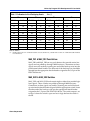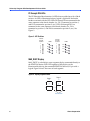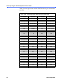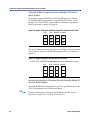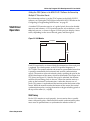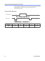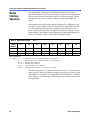
1
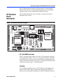
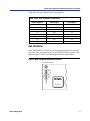
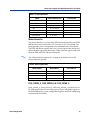
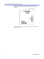
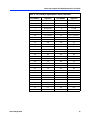
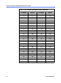
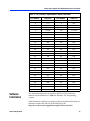
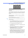
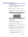
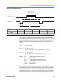
® University Program UP2 Development Kit July 2003, v3.0 Introduction User Guide The University Program UP2 Development Kit was designed to meet the needs of universities teaching digital logic design with state-of-the-art development tools and programmable logic devices (PLDs). The package provides all of the necessary tools for creating and implementing digital logic designs, including the following features: ■ ■ ■ MAX+PLUS® II University development software UP Education Board – An EPF10K70 device for the UP2 board in a 240-pin power quad flat pack (RQFP) package – An 84-pin plastic J-lead chip carrier (PLCC) package ByteBlasterTM II parallel port download cable MAX+PLUS II University Software The MAX+PLUS II University software contains many of the features of the commercial version of the MAX+PLUS II software including a completely integrated design flow and an intuitive graphical user interface. This software supports schematic capture and text-based hardware description language (HDL) design entry, including Verilog HDL, VHDL, and the Altera® Hardware Description Language (AHDLTM). It also provides design programming, compilation, and verification support for all devices supported by the MAX+PLUS II BASELINE software including the EPM7128S, and EPF10K70 devices. The MAX+PLUS II University software can be freely distributed to students for installation on their personal computers and provides instant access to online help. 1 For information on how to install the MAX+PLUS II University software on your computer, see “Software Installation” on page 17. UP2 Education Board The UP2 Education Board is a stand-alone experiment board based on a FLEX® 10K device and includes a MAX® 7000 device. When used with the MAX+PLUS II University software, the board provides a superior platform for learning digital logic design using industry-standard development tools and PLDs. Altera Corporation A-UG-UP1-3.0 P25-09231-00 1 University Program UP2 Development Kit User Guide The board is designed to meet the needs of instructors and students in a laboratory environment. The UP2 Education Board supports both look-up table (LUT) -based and product term-based architectures. The EPF10K70 device can be configured in-system with either the ByteBlaster II download cable or an EPC1 configuration device. Additional download cables can be purchased separately. The EPM7128S device can be programmed in-system with the ByteBlaster II download cable. EPF10K70 Device The EPF10K70 device is based on SRAM technology. It is available in a 240-pin RQFP package and has 3,744 logic elements (LEs) and nine embedded array blocks (EABs). Each LE consists of a four-input LUT, a programmable flipflop, and dedicated signal paths for carry-and-cascade functions. Each EAB provides 2,048 bits of memory which can be used to create RAM, ROM, or first-in first-out (FIFO) functions. EABs can also implement logic functions, such as multipliers, microcontrollers, state machines, and digital signal processing (DSP) functions. With 70,000 typical gates, the EPF10K70 device is ideal for intermediate to advanced digital design courses, including computer architecture, communications, and DSP applications. f For more information on FLEX 10K devices, see the FLEX 10K Embedded Programmable Logic Family Data Sheet. EPM7128S Device The EPM7128S device, a member of the high-density, high-performance MAX 7000S family, is based on erasable programmable read-only memory (EEPROM) elements. The EPM7128S device features a socketmounted 84-pin plastic j-lead chip carrier (PLCC) package and has 128 macrocells. Each macrocell has a programmable-AND/fixed-OR array as well as a configurable register with independently-programmable clock, clock enable, clear, and preset functions. With a capacity of 2,500 gates and a simple architecture, the EPM7128S device is ideal for introductory designs as well as larger combinatorial and sequential logic functions. f For more information on MAX 7000 devices, go to the MAX 7000 Programmable Logic Device Family Data Sheet. ByteBlaster II Parallel Port Download Cable Designs can be easily and quickly downloaded into the UP2 Education Board using the ByteBlaster II download cable, which is a hardware interface to a standard parallel port. This cable sends programming or configuration data between the MAX+PLUS II University software and 2 Altera Corporation University Program UP2 Development Kit User Guide the UP Education Boards. Because design changes are downloaded directly to the devices on the board, prototyping is easy and multiple design iterations can be accomplished in quick succession. UP Education Board Description The UP2 Education Board, shown in Figure 1, contains the features described in this section. MOUSE + FLEX_EXPAN_ VGA FLEX_DIGIT CONF_D TCK POWER – DC + EPC1 P1 P2 D2 D3 EPM7128S P4 D4 D5 MAX_DIGIT D9 D10 D6 D11 D7 D12 D8 P8 P10 MAX_PB2 P6 P9 MAX_SW2 MAX_PB1 MAX_SW1 P5 FLEX_SWITCH D15 D16 JTAG_OUT P3 D13 D14 FLEX_PB1 FLEX_PB2 P7 D1 EPF10K20 EPF10K70 or EPF10K70 FLEX_EXPAN_ C2 TDI TDO BOARD C19 U5 RAW – R2 R1 DC_IN DEVICE MAX_EXPANSION JTAG_IN Figure 1. UP2 Education Board Block Diagram FLEX_EXPAN_ DC_IN & RAW Power Input The DC_IN power input accepts a 2.5-mm × 5.55-mm female connector. The acceptable DC input is 7 to 9 V at a minimum of 350 mA. The RAW power input consists of two holes for connecting an unregulated power source. The hole marked with a plus sign (+) is the positive input; the hole marked with a minus sign (–) is board-common. Oscillator The UP Education Board contains a 25.175-MHz crystal oscillator. The output of the oscillator drives a global clock input on the EPM7128S device (pin 83) and a global clock input on the FLEX 10K device (pin 91). Altera Corporation 3 University Program UP2 Development Kit User Guide JTAG_IN Header The 10-pin female plug on the ByteBlaster II download cable connects with the JTAG_IN 10-pin male header on the UP Education Board. The board provides power and ground to the ByteBlaster II download cable. Data is shifted into the devices via the TDI pin and shifted out of the devices via the TDO pin. Table 1 identifies the JTAG_IN pin names when the ByteBlaster II is operating in Joint Test Action Group (JTAG) mode. Table 1. JTAG_IN 10-Pin Header Pin-Outs Pin JTAG Signal 1 TCK 2 GND 3 TDO 4 VCC 5 TMS 6 No Connect 7 No Connect 8 No Connect 9 TDI 10 GND Jumpers The UP Education Board has four three-pin jumpers (TDI, TDO, DEVICE, and BOARD) that set the JTAG configuration. The JTAG chain can be set for a variety of configurations (i.e., to program only the EPM7128S device, to configure only the FLEX 10K device, to configure and program both devices, or to connect multiple UP Education Boards together). Figure 2 shows the positions of the three connectors (C1, C2, and C3) on each of the four jumpers. 4 Altera Corporation University Program UP2 Development Kit User Guide Figure 2. Position of C1, C2 & C3 Connectors TDI TDO DEVICE BOARD C1 C1 C1 C1 C2 C2 C2 C2 C3 C3 C3 C3 Table 2 defines the settings for each configuration. Table 2. JTAG Jumper Settings Desired Action TDI TDO DEVICE BOARD Program EPM7128S device only C1 & C2 C1 & C2 C1 & C2 C1 & C2 Configure FLEX 10K device only C2 & C3 C2 & C3 C1 & C2 C1 & C2 Program/configure both devices (1) C2 & C3 C1 & C2 C2 & C3 C1 & C2 Connect multiple boards together (2) C2 & C3 OPEN C2 & C3 C2 & C3 Notes to Table 2: (1) (2) The first device in the JTAG chain is the FLEX 10K device, and the second device is the EPM7128S device. The first device in the JTAG chain is the FLEX 10K device, and the second device is the EPM7128S device. The last board in the chain must be set for a single board configuration (i.e., for programming only the EPM7128S device, configuring only the FLEX 10K device, or configuring/programming both devices). The last board cannot be set for connecting multiple boards together. During configuration, the green CONF_D LED will turn off and the green TCK LED will modulate to indicate that data is transferring. After the device has successfully configured, the CONF_D LED will illuminate. f Altera Corporation For information on how to program or configure the EPF10K70, or EPM7128S devices, see “Programming or Configuring Devices” on page 18. 5 University Program UP2 Development Kit User Guide EPM7128S Device The UP2 Education Board provides the following resources for the EPM7128S device. ■ ■ ■ ■ ■ ■ ■ ■ ■ Socket-mounted 84-pin PLCC package Signal pins that are accessible via female headers JTAG chain connection for the ByteBlaster II cable Two momentary push-button switches Two octal dual inline package (DIP) switches 16 LEDs Dual-digit seven-segment display On-board oscillator (25.175 MHz) Expansion port with 42 I/O pins and the dedicated global CLR, OE1, and OE2/GCLK2 pins Pins from the EPM7128S device are not pre-assigned to switches and LEDs, but are instead connected to female headers. With direct access to the pins, students can concentrate on design fundamentals and learn about the programmability of I/O pins and PLDs. After successfully compiling and verifying a design with the MAX+PLUS II University software, students can easily connect the assigned I/O pins to the switches and LEDs using a common hook-up wire. Students can then download their design into the device and compare their design’s simulation to the actual hardware implementation. EPM7128S Prototyping Headers The EPM7128S prototyping headers are female headers that surround the device and provide access to the device’s signal pins. The 21 pins on each side of the 84-pin PLCC package connect to one of the 22-pin, dual-row 0.1-inch female headers. The pin numbers for the EPM7128S device are printed on the UP2 Education Board (an “X” indicates an unassigned pin). Table 3 lists the pin numbers for the four female headers: P1, P2, P3, and P4. The power, ground, and JTAG signal pins are not accessible through these female headers. 6 Altera Corporation University Program UP2 Development Kit User Guide Table 3. Pin Numbers for Each Prototyping Header P1 Note (1) P2 P3 P4 Outside Inside Outside Inside Outside Inside Outside Inside 75 76 12 13 33 34 54 55 77 78 14 15 35 36 56 57 79 80 16 17 37 38 58 59 81 82 18 19 39 40 60 61 83 84 20 21 41 42 62 63 1 2 22 23 43 44 64 65 3 4 24 25 45 46 66 67 5 6 26 27 47 48 68 69 7 8 28 29 49 50 70 71 9 10 30 31 51 52 72 73 11 X 32 X 53 X 74 X Note to Table 3: (1) Inside refers to the row of female headers closest to the device; outside refers to the row of female headers furthest from the device. MAX_PB1 & MAX_PB2 Push-Buttons MAX_PB1 and MAX_PB2 are two push-buttons that provide active-low signals and are pulled-up through 10-KΩ resistors. Connections to these signals are easily made by inserting one end of the hook-up wire into the push-button female header. The other end of the hook-up wire should be inserted into the appropriate female header assigned to the I/O pin of the EPM7128S device. MAX_SW1 & MAX_SW2 Switches MAX_SW1 and MAX_SW2 each contain eight switches that provide logiclevel signals. These switches are pulled-up through 10-KΩ resistors. Connections to these signals are made by inserting one end of the hookup wire into the female header aligned with the appropriate switch. Insert the other end of the hook-up wire into the appropriate female header assigned to the I/O pin of the EPM7128S device. The switch output is set to logic 1 when the switch is open and set to logic 0 when the switch is closed. Altera Corporation 7 University Program UP2 Development Kit User Guide D1 through D16 LEDs The UP Education Board contains 16 LEDs that are pulled-up with a 330-Ω resistor. An LED is illuminated when a logic 0 is applied to the female header associated with the LED. LEDs D1 through D8 are connected in the same sequence to the female headers (i.e., D1 is connected to position 1, and D2 is connected to position 2, etc.). LEDs D9 through D16 are connected in the same sequence to the female headers (i.e., D9 is connected to position 1, and D10 is connected to position 2, etc.). See Figure 3. Figure 3. LED Positions Female Header Position Female Header Position LEDs 1 2 3 4 5 6 7 8 D1 1 2 3 4 5 6 7 8 D5 D2 D6 D3 D7 D4 D8 LEDs D9 D13 D10 D14 D11 D15 D12 D16 MAX_DIGIT Display MAX_DIGIT is a dual-digit, seven-segment display connected directly to the EPM7128S device. Each LED segment of the display can be illuminated by driving the connected EPM7128S device I/O pin with a logic 0. Figure 4 shows the name of each segment. Figure 4. Display Segment Name f Digit 1 Digit 2 a a g e d b f c e g b c d Decimal Point 8 Altera Corporation University Program UP2 Development Kit User Guide Table 4 lists the pin assignments for each segment. Table 4. MAX_DIGIT Segment I/O Connections Display Segment Pin for Digit 1 Pin for Digit 2 a 58 69 b 60 70 c 61 73 d 63 74 e 64 76 f 65 75 g 67 77 Decimal point 68 79 MAX_EXPANSION MAX_EXPANSION is a dual row of 0.1-inch-spaced holes for accessing signal I/O pins and global signals on the EPM7128S device, power, and ground. Figure 5 shows the numbering convention for the holes. Figure 5. MAX_EXPANSION Numbering Convention 1 3 5 7 9 11 13 15 4 6 8 10 12 14 16 MAX_EXPANSION UP Education Board ® EPM7128S Altera Corporation 9 University Program UP2 Development Kit User Guide Table 5 lists the signal names and the EPM7128S device pins connected to each hole. Table 5. MAX_EXPANSION Signal Names & Device Connections 10 Hole Number Signal/Pin Hole Number Signal/Pin 1 RAW 2 GND 3 VCC 4 GND 5 VCC 6 GND 7 No Connect 8 No Connect No Connect 9 No Connect 10 11 No Connect 12 GCLRn/1 13 OE1/84 14 OE2/GCLK2/2 15 4 16 17 6 18 5 8 19 9 20 10 21 11 22 12 23 15 24 16 25 17 26 18 27 20 28 21 29 22 30 25 31 24 32 27 33 29 34 28 35 31 36 30 37 33 38 34 39 35 40 36 41 37 42 40 43 39 44 41 45 44 46 46 47 45 48 48 49 50 50 49 51 52 52 51 53 54 54 55 55 56 56 57 57 VCC 58 GND 59 VCC 60 GND Altera Corporation University Program UP2 Development Kit User Guide FLEX 10K Device The UP2 Education Board provides the following resources for the FLEX 10K device. The pins from the FLEX 10K device are pre-assigned to switches and LEDs on the board. ■ ■ ■ ■ ■ ■ ■ ■ ■ JTAG chain connection for the ByteBlaster II cable Socket for an EPC1 configuration device Two momentary push button switches One octal DIP switch Dual-digit seven-segment display On-board oscillator (25.175 MHz) VGA port Mouse port Three expansion ports, each with 42 I/O pins and seven global pins FLEX_PB1 & FLEX_PB2 Push Buttons FLEX_PB1 and FLEX_PB2 are two push buttons that provide active-low signals to two general-purpose I/O pins on the FLEX 10K device. FLEX_PB1 connects to pin 28, and FLEX_PB2 connects to pin 29. Each push button is pulled-up through a 10-KΩ resistor. FLEX_SW1 Switches FLEX_SW1 contains eight switches that provide logic-level signals to eight general-purpose I/O pins on the FLEX 10K device. An input pin is set to logic 1 when the switch is open and set to logic 0 when the switch is closed. Table 6 lists the pin assignment for each switch. Table 6. FLEX_SW1 Pin Assignments Altera Corporation Switch FLEX 10K Pin FLEX_SWITCH-1 41 FLEX_SWITCH-2 40 FLEX_SWITCH-3 39 FLEX_SWITCH-4 38 FLEX_SWITCH-5 36 FLEX_SWITCH-6 35 FLEX_SWITCH-7 34 FLEX_SWITCH-8 33 11 University Program UP2 Development Kit User Guide FLEX_DIGIT Display FLEX_DIGIT is a dual-digit, seven-segment display connected directly to the FLEX 10K device. Each LED segment on the display can be illuminated by driving the connected FLEX 10K device I/O pin with a logic 0. See Figure 4 on page 8 for the name of each segment. Table 7 lists the pin assignment for each segment. Table 7. FLEX_DIGIT Segment I/O Connections Display Segment Pin for Digit 1 Pin for Digit 2 a 6 17 b 7 18 c 8 19 d 9 20 e 11 21 f 12 23 g 13 24 Decimal point 14 25 VGA Interface The VGA interface allows the FLEX 10K device to control an external video monitor. This interface is composed of a simple diode-resistor network and a 15-pin D-sub connector (labeled VGA), where the monitor can plug into the boards. The diode-resistor network and D-sub connector are designed to generate voltages that conform to the VGA standard. Information about the color, row, and column indexing of the screen is sent from the FLEX 10K device to the monitor via five signals. Three VGA signals are red, green, and blue, while the other two signals are horizontal and vertical synchronization. Manipulating these signals allows images to be written to the monitor’s screen. f See “VGA Driver Operation” on page 25 for details on how the VGA interface operates. Table 8 lists the D-sub connector and the FLEX 10K device connections. 12 Altera Corporation University Program UP2 Development Kit User Guide Table 8. D-Sub Connections Signal D-Sub Connector Pin FLEX 10K Pin RED 1 236 GREEN 2 237 BLUE 3 238 GND 6, 7, 8, 10, 11 HORIZ_SYNC 13 240 VERT_SYNC 14 239 No Connect 4, 5, 9, 15 – – Mouse Connector The mouse interface, is a six-pin mini-DIN connector that allows the FLEX 10K device to receive data from a PS/2 mouse or a PS/2 keyboard. The board provides power and ground to the attached mouse or keyboard. The FLEX 10K device outputs the DATA_CLOCK signal to the mouse and inputs the data signal from the mouse. Table 9 lists the signal names and the mini-DIN and FLEX 10K pin connections. f See “Mouse Interface Operation” on page 28 for details on how the mouse interface operates. Table 9. Mouse Connections Mouse Signal Mini-DIN Pin FLEX 10K Pin MOUSE_CLK 1 30 MOUSE_DATA 3 31 VCC 5 – GND 2 – FLEX_EXPAN_A, FLEX_EXPAN_B & FLEX_EXPAN_C FLEX_EXPAN_A, FLEX_EXPAN_B, and FLEX_EXPAN_C are dual rows of 0.1-inch spaced holes for accessing signal I/O pins and global signals on the FLEX 10K device, power, and ground. Figure 6 shows the numbering convention for these holes. Altera Corporation 13 University Program UP2 Development Kit User Guide Figure 6. FLEX_EXPAN_A, FLEX_EXPAN_B & FLEX_EXPAN_C Numbering Convention UP Education Board 15 13 11 9 7 5 3 1 16 14 12 10 8 6 4 2 A C AN_ A 2 4 6 8 10 14 16 FLEX_EXP P B 16 12 10 8 6 4 2 15 13 11 9 7 5 3 1 1 3 5 7 9 1113 15 Tables 10 through 12 list the signal name and the FLEX 10K device pin connected to each hole. 14 Altera Corporation University Program UP2 Development Kit User Guide Table 10. FLEX_EXPAN_A Signal Names & Device Connections Hole Number Altera Corporation Signal/Pin Hole Number Signal/Pin 1 RAW 2 GND 3 VCC 4 GND 5 VCC 6 GND 7 No Connect 8 DI1/90 9 DI2/92 10 DI3/210 11 DI4/212 12 DEV_CLR/209 13 DEV_OE/213 14 DEV_CLK2/211 15 45 16 46 17 48 18 49 19 50 20 51 21 53 22 54 23 55 24 56 25 61 26 62 27 63 28 64 29 65 30 66 31 67 32 68 33 70 34 71 35 72 36 73 37 74 38 75 39 76 40 78 41 79 42 80 43 81 44 82 45 83 46 84 47 86 48 87 49 88 50 94 51 95 52 97 53 98 54 99 55 100 56 101 57 VCC 58 GND 59 VCC 60 GND 15 University Program UP2 Development Kit User Guide Table 11. FLEX_EXPAN_B Signal Names & Device Connections Hole Number 16 Signal/Pin Hole Number Signal/Pin 1 RAW 2 GND 3 VCC 4 GND 5 VCC 6 GND 7 No Connect 8 DI1/90 9 DI2/92 10 DI3/210 11 DI4/212 12 DEV_CLR/209 13 DEV_OE/213 14 DEV_CLK2/211 15 109 16 110 17 111 18 113 19 114 20 115 21 116 22 117 23 118 24 119 25 120 26 126 27 127 28 128 29 129 30 131 31 132 32 133 33 134 34 136 35 137 36 138 37 139 38 141 39 142 40 143 41 144 42 146 43 147 44 148 45 149 46 151 47 152 48 153 49 154 50 156 51 157 52 158 53 159 54 161 55 162 56 163 57 VCC 58 GND 59 VCC 60 GND Altera Corporation University Program UP2 Development Kit User Guide Table 12. FLEX_EXPAN_C Signal Names & Device Connections Hole Number Software Installation Signal/Pin Hole Number Signal/Pin 1 RAW 2 GND 3 VCC 4 GND 5 VCC 6 GND 7 No Connect 8 DI1/90 9 DI2/92 10 DI3/210 11 DI4/212 12 DEV_CLR/209 13 DEV_OE/213 14 DEV_CLK2/211 15 175 16 181 17 182 18 183 19 184 20 185 21 186 22 187 23 188 24 190 25 191 26 192 27 193 28 194 29 195 30 196 31 198 32 199 33 200 34 201 35 202 36 203 37 204 38 206 39 207 40 208 41 214 42 215 43 217 44 218 45 219 46 220 47 221 48 222 49 223 50 225 51 226 52 227 53 228 54 229 55 230 56 231 57 VCC 58 GND 59 VCC 60 GND This section describes how to install the MAX+PLUS II University software for the Windows 98/2000 and Windows NT 4.0 operating systems. After installation, students can register to obtain an authorization code via the Altera world-wide web site at the following URL: http://www.altera.com/support/licensing/lic-university.html. Altera Corporation 17 University Program UP2 Development Kit User Guide f For complete installation instructions, refer to the readme file on the MAX+PLUS II University CD-ROM ,or see the MAX+PLUS II Getting Started manual. Windows 98/2000 & Windows NT 4.0 Follow the below steps to install the MAX+PLUS II University software onto a PC. Programming or Configuring Devices 1. Insert the MAX+PLUS II University CD-ROM into the CD-ROM drive. 2. Choose Run (Start menu). 3. Type: <CD-ROM drive>:\mp2_101se.exe and click OK. The Setup Wizard will guide you through the installation procedure. Programming or configuring the devices on the UP Education Boards requires setting the on-board jumpers and the JTAG programming options in the MAX+PLUS II software, and connecting the ByteBlaster II download cable to the PC’s parallel port and to the JTAG_IN connector on the UP Education Boards. This section describes how to set these options. ■ ■ ■ ■ Program only the EPM7128S device Configure only the EPF10K70 device Configure/program both devices Connect multiple UP Education Boards together in a chain EPM7128S Programming This section describes the procedures for programming only EPM7128S devices, (i.e., how to set the on-board jumpers, connect the ByteBlaster II download cable, and set options in the MAX+PLUS II software). Setting the On-Board Jumpers for EPM7128S Programming To program only the EPM7128S device in a JTAG chain, set the jumpers TDI, TDO, DEVICE, and BOARD as shown in Figure 7. 18 Altera Corporation University Program UP2 Development Kit User Guide Figure 7. Jumper Settings for Programming Only the EPM7128S Device TDI TDO DEVICE BOARD C1 C1 C1 C1 C2 C2 C2 C2 C3 C3 C3 C3 Connecting the ByteBlaster II Download Cable for EPM7128S Programming Attach the ByteBlaster II cable directly to the PC’s parallel port and to the JTAG_IN connector on the board. For more information on setting up the ByteBlaster II cable, go to the ByteBlaster II Parallel Port Download Cable Data Sheet. Setting the JTAG Options in the MAX+PLUS II Software for EPM7128S Device Programming The following steps describe how to use the MAX+PLUS II software to program the EPM7128S device in a JTAG chain. f Altera Corporation For more information on how to use the MAX+PLUS II software, see the MAX+PLUS II Help. 1. Turn on the Multi-Device JTAG Chain command (JTAG menu) in the MAX+PLUS II Programmer to program a device. Follow this procedure even if you are only programming one device. 2. Choose Multi-Device JTAG Chain Setup (JTAG menu). 3. Select EPM7128S in the Device Name list in the Multi-Device JTAG Chain Setup dialog box. 4. Type the name of the programming file for the EPM7128S device in the Programming File Name box. You can use the Select Programming File button to browse a computer’s directory structure to locate the appropriate programming file. 5. Click Add to add the device and associated programming file to the Device Names & Programming File Names box. The number to the left of the device name shows the order of the device in the JTAG chain. The device’s associated programming file is displayed on the same line as the device name. If no programming file is associated with a device, “<none>” is displayed next to the device name. 19 University Program UP2 Development Kit User Guide 6. Click Detect JTAG Chain Info to have the ByteBlaster II cable check the device count, JTAG ID code, and total instruction length of the JTAG chain. A message just above the Detect JTAG Chain Info button reports the information detected by the ByteBlaster II cable. This message must be manually verified to match the information in the Device Names & Programming File Names box. 7. Click Save JCF. In the Save JCF dialog box, type the name of the file in the File Name box and then select the desired directory in the Directories box to save the current settings to a JTAG Chain File (.jcf) for future use. Click OK. 8. Click OK to save changes. 9. Click Program in the MAX+PLUS II Programmer. EPF10K70 Configuration This section describes the procedures for configuring the EPF10K70 device (i.e., how to set the on-board jumpers, connect the ByteBlaster II download cable, and set options in the MAX+PLUS II software). Setting the On-Board Jumpers for EPF10K70 Configuration To configure the EPF10K70 device in a JTAG chain, set the jumpers TDI, TDO, DEVICE, and BOARD as shown in Figure 8. Figure 8. Jumper Settings for Configuring Only the FLEX 10K Device TDI TDO DEVICE BOARD C1 C1 C1 C1 C2 C2 C2 C2 C3 C3 C3 C3 Connecting the ByteBlaster II Download Cable for the EPF10K70 Configuration Attach the ByteBlaster II cable directly to the PC’s parallel port and to the JTAG_IN connector on the UP Education Board. For more information on setting up the ByteBlaster II cable, see the ByteBlaster II Parallel Port Download Cable Data Sheet. 20 Altera Corporation University Program UP2 Development Kit User Guide Setting the JTAG Options in the MAX+PLUS II Software for EPF10K70 Configuration The following steps describe how to use the MAX+PLUS II software to configure the EPF10K70 device in a JTAG chain. f Altera Corporation For more information on how to configure a device, see the MAX+PLUS II Help. 1. Turn on the Multi-Device JTAG Chain command (JTAG menu) in the MAX+PLUS II Programmer to configure the EPF10K70 device. Follow this step even if you are only programming one device. 2. Choose Multi-Device JTAG Chain Setup (JTAG menu). 3. Select EPF10K70 in the Device Name list in the Multi-Device JTAG Chain Setup dialog box. 4. Type the name of the programming file for the EPF10K70 device in the Programming File Name box. You can also use the Select Programming File button to browse your computer’s directory structure to locate the appropriate programming file. 5. Click Add to add the device and associated programming file to the Device Names & Programming File Names box. The number to the left of the device name shows the order of the device in the JTAG chain. The device’s associated programming file is displayed on the same line as the device name. If no programming file is associated with a device, “<none>” is displayed next to the device name. 6. Click Detect JTAG Chain Info to have the ByteBlaster II cable check the device count, JTAG ID code, and total instruction length of the JTAG chain. A message just above the Detect JTAG Chain Info button reports the information detected by the ByteBlaster II cable. You must manually verify that this message matches the information in the Device Names & Programming File Names box. 7. Click Save JCF to save the current settings to a JCF for future use. Type the name of the file in the File Name box and then select the desired directory in the Directories box in the Save JCF dialog box. Click OK. 8. Click OK to save your changes. 9. Click Configure in the MAX+PLUS II Programmer. 21 University Program UP2 Development Kit User Guide Configure/Program Both Devices This section describes the procedures for configuring/programming both the FLEX 10K and EPM7128S devices in a JTAG chain, (i.e., how to set the on-board jumpers, connect the ByteBlaster II download cable, and set options in the MAX+PLUS II software). Setting the On-Board Jumpers for Configuring/Programming Both Devices To configure and program the FLEX 10K and EPM7128S devices in a multi-device JTAG chain, set the jumpers TDI, TDO, DEVICE, and BOARD as shown in Figure 9. Figure 9. Jumper Settings for Configuring/Programming Both Devices TDI TDO DEVICE BOARD C1 C1 C1 C1 C2 C2 C2 C2 C3 C3 C3 C3 Connecting the ByteBlaster II Download Cable for Configuring & Programming Both Devices Attach the ByteBlaster II cable directly to the PC’s parallel port and to the JTAG_IN connector on the UP Education Board. For more information on setting up the ByteBlaster II cable, see the ByteBlaster II Parallel Port Download Cable Data Sheet. Setting the JTAG Options in the MAX+PLUS II Software for Configuring & Programming Both Devices The following steps describe how to use the MAX+PLUS II software to configure and program both devices in a multi-device JTAG chain. For more information on how to program or configure a device, see the MAX+PLUS II Help. 22 1. Turn on the Multi-Device JTAG Chain command (JTAG menu). 2. Choose Multi-Device JTAG Chain Setup (JTAG menu). 3. Select the first target device name in the Device Name list in the Multi-Device JTAG Chain Setup dialog box. Altera Corporation University Program UP2 Development Kit User Guide 4. Type the name of the programming file for the device listed in the Device Name box in the Programming File Names box. The Select Programming File button can also be used to browse your computer’s directory structure to locate the appropriate programming file. 5. Click Add to add the device and associated programming file to the Device Names & Programming File Names box. The number to the left of the device name shows the device’s order in the JTAG chain. The device’s associated programming file is displayed on the same line as the device name. If no programming file is associated with a device, “<none>” is displayed next to the device name. 6. Repeat steps 3 through 5 to add information for each device in the JTAG chain. 7. Click Detect JTAG Chain Info to have the ByteBlaster II cable check the device count, JTAG ID code, and total instruction length of the multi-device JTAG chain. A message just above the Detect JTAG Chain Info button reports the information detected by the ByteBlaster II cable. You must manually verify that this message matches the information in the Device Names & Programming File Names box. 8. Click Save JCF to save the current settings to a JCF for future use. Type the name of the file in the File Name box and then select the desired directory in the Directories box. Click OK. 9. Click OK to save the changes. 10. Click Configure in the MAX+PLUS II Programmer to configure all FLEX 10K devices in the JTAG chain. Then, click Program to program all EPM7128S devices in the JTAG chain. Connect Multiple UP Education Boards Together in a Chain This section describes the procedures for connecting multiple UP Education Boards together (i.e., how to set the on-board jumpers, connect the ByteBlaster II download cable, and set options in the MAX+PLUS II software). Altera Corporation 23 University Program UP2 Development Kit User Guide Setting the On-Board Jumpers for Connecting Multiple UP Education Boards Together To configure/program EPM7128S and FLEX 10K devices on multiple UP Education Boards connected in a multi-device JTAG chain, set the jumpers TDI, TDO, DEVICE, and BOARD for all boards except the last board in the chain as shown in Figure 10. Figure 10. Jumper Settings for All Boards Except the Last Board in the Chain TDI TDO DEVICE BOARD C1 C1 C1 C1 C2 C2 C2 C2 C3 C3 C3 C3 The last UP Education Board in the chain can configure and program one or both devices. However, the BOARD jumper must be set as shown in Figure 11. Figure 11. Jumper Settings for the Last Board in the Chain The TDI, TDO, and DEVICE settings depend on which configuration is used. TDI TDO DEVICE BOARD C1 C1 C1 C1 C2 C2 C2 C2 C3 C3 C3 C3 Connecting the ByteBlaster II Download Cable for Connecting Multiple UP Education Boards Together Attach the ByteBlaster II cable directly to your PC’s parallel port and to the JTAG_IN connector on the UP Education Board. f 24 For more information on setting up the ByteBlaster II cable, see the ByteBlaster II Parallel Port Download Cable Data Sheet. Altera Corporation University Program UP2 Development Kit User Guide Setting the JTAG Options in the MAX+PLUS II Software for Connecting Multiple UP Education Boards For information on how to set the JTAG options in the MAX+PLUS II software, see “Setting the JTAG Options in the MAX+PLUS II Software for Configuring & Programming Both Devices” on page 22. VGA Driver Operation A standard VGA monitor consists of a grid of pixels that can be divided into rows and columns. A VGA monitor contains at least 480 rows, with 640 pixels per row, as shown in Figure 12. Each pixel can display various colors, depending on the state of the red, green, and blue signals. Figure 12. VGA Monitor 640 pixels (0,0) 480 pixels (640, 480) Each VGA monitor has an internal clock that determines when each pixel is updated. This clock operates at the VGA-specified frequency of 25.175 MHz. The monitor refreshes the screen in a prescribed manner that is partially controlled by the horizontal and vertical synchronization signals. The monitor starts each refresh cycle by updating the pixel in the top left-hand corner of the screen, which can be treated as the origin of an X–Y plane (see Figure 12). After the first pixel is refreshed, the monitor refreshes the remaining pixels in the row. When the monitor receives a pulse on the horizontal synchronization, it refreshes the next row of pixels. This process is repeated until the monitor reaches the bottom of the screen. When the monitor reaches the bottom of the screen, the vertical synchronization pulses, causing the monitor to begin refreshing pixels at the top of the screen (i.e., at [0,0]). VGA Timing For the VGA monitor to work properly, it must receive data at specific times with specific pulses. Horizontal and vertical synchronization pulses must occur at specified times to synchronize the monitor while it is Altera Corporation 25 University Program UP2 Development Kit User Guide receiving color data. Figures 13 and 14 show the timing waveforms for the color information with respect to the horizontal and vertical synchronization signals. Figure 13. Horizontal Refresh Cycle RED, GREEN, BLUE C E D HORIZ_SYNC B A 26 Parameters A B C D E Time 31.77 µs 3.77 µs 1.89 µs 25.17 µs 0.94 µs Altera Corporation University Program UP2 Development Kit User Guide Figure 14. Vertical Refresh Cycle 480 Horizontal Refresh Cycles RED, GREEN, BLUE Q S R VERT_SYNC P O Parameters O P Q R S Time 16.6 ms 64 µs 1.02 ms 15.25 ms 0.35 ms The frequency of operation and the number of pixels that the monitor must update determines the time required to update each pixel, and the time required to update the whole screen. The following equations roughly calculate the time required for the monitor to perform all of its functions. Tpixel = 1/fCLK = 40 ns TROW = = A=B+C+D+E (Tpixel × 640 pixels) + row + guard bands = 31.77 µs Tscreen = = O=P+Q+R+S (TROW × 480 rows) + guard bands = 16.6 ms Where: Tpixel fCLK TROW Tscreen B, C, E P, Q, S = = = = = = Time required to update a pixel 25.175 MHz Time required to update one row Time required to update the screen Guard bands Guard bands The monitor writes to the screen by sending red, green, blue, horizontal synchronization, and vertical synchronization signals when the screen is at the expected location. Once the timing of the horizontal and vertical synchronization signals is accurate, the monitor only needs to keep track of the current location, so it can send the correct color data to the pixel. Altera Corporation 27 University Program UP2 Development Kit User Guide Mouse Interface Operation You can connect a mouse to the UP Education Board via the 6-pin mini-DIN connector. The data is sent using a synchronous serial protocol, and the transmission is controlled by the CLK and DATA signals. During non-transmission, CLK is at logic 1 and DATA can be either logic 0 or logic 1. Each transmission contains one start bit, eight data bits, odd parity, and one stop bit. Data transmission starts from the least significant bit (LSB), (i.e., the sequence of transmission is start bit, DATA0 through DATA7, parity, and stop bit). Start bits are logic 0, and stop bits are logic 1. Each clock period is 30 to 50 µsec; the data transition to the falling edge of the clock is 5 to 25 µsec. Table 13 shows the data packet format. Table 13. Data Packet Format Note (1) Packet Number D7 D6 D5 D4 D3 D2 D1 D0 1 YV XV YS XS 1 0 R L 2 X7 X6 X5 X4 X3 X2 X1 X0 3 Y7 Y6 Y5 Y4 Y3 Y2 Y1 Y0 Note to Table 13: (1) Where: L R X0 – X7 Y0 – Y7 XS, YS XV, YV = = = = = = Left button state (1 = left mouse button is pressed down) Right button state (1 = right mouse button is pressed down) Movement in X direction Movement in Y direction Movement data sign (1 = negative) Movement data overflow (1 = overflow has occurred) The mouse operates on a Cartesian coordinate system (i.e., moving to the right is positive, moving to the left is negative, moving up is positive, and moving down is negative). The magnitude of the movement is a function of the mouse’s rate of movement. The faster the mouse moves, the greater the magnitude. 28 Altera Corporation Notes: Altera Corporation 29 University Program UP2 Development Kit User Guide ® 101 Innovation Drive San Jose, CA 95134 (408) 544-7000 http://www.altera.com University Program: [email protected] Literature Services: (888) 3-ALTERA [email protected] 30 Altera, MAX, MAX+PLUS, MAX+PLUS II, MAX 7000S, EPM7128S, FLEX, FLEX 10K, EPF10K20, EPF10K70, ByteBlasterMV, EPC1, and AHDL are trademarks and/or service marks of Altera Corporation in the United States and other countries. Altera acknowledges the trademarks of other organizations for their respective products or services mentioned in this document. Altera products are protected under numerous U.S. and foreign patents and pending applications, maskwork rights, and copyrights. Altera warrants performance of its semiconductor products to current specifications in accordance with Altera’s standard warranty, but reserves the right to make changes to any products and services at any time without notice. Altera assumes no responsibility or liability arising out of the application or use of any information, product, or service described herein except as expressly agreed to in writing by Altera Corporation. Altera customers are advised to obtain the latest version of device specifications before relying on any published information and before placing orders for products or services. Copyright 2001 Altera Corporation. All rights reserved. Altera Corporation Printed on Recycled Paper.