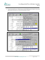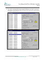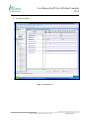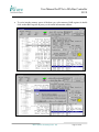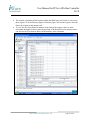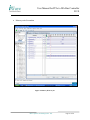
1
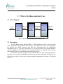
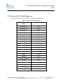
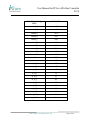
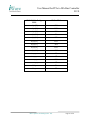
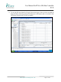
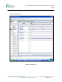
User Manual for PCIe to ISA Bus Controller R 2.0 User Manual for PCIe ISA Bus Controller iWave Systems Technologies Pvt. Ltd. Page 1 of 26 User Manual for PCIe to ISA Bus Controller R 2.0 Table of Contents 1 INTRODUCTION................................................................................................................. 4 1.1 1.2 1.3 1.4 2 PCIE TO ISA BUS CONTROLLER CORE ...................................................................... 6 2.1 2.2 2.3 3 PURPOSE .......................................................................................................................... 4 SCOPE .............................................................................................................................. 4 FEATURES ........................................................................................................................ 4 EVALUATION BOARD AND CORE REQUIREMENTS ............................................................ 5 BLOCK DIAGRAM ............................................................................................................. 6 DESCRIPTION ................................................................................................................... 6 PIN OUTS OF IW- PCIE ISA BRIDGE CORE........................................................................ 7 QUICK START ................................................................................................................... 11 3.1 CONNECTING TO A HOST COMPUTER.............................................................................. 11 3.1.1 Installation Requirements ......................................................................................... 11 3.1.2 Board Installation & Testing .................................................................................... 11 3.1.3 Procedure for Demo ................................................................................................. 12 APPENDIX A .............................................................................................................................. 26 iWave Systems Technologies Pvt. Ltd. Page 2 of 26 User Manual for PCIe to ISA Bus Controller R 2.0 List of Figures Figure 1: Detailed view of iW-PCIe to ISA controller core ........................................................... 6 Figure 2: IO Write Cycle .............................................................................................................. 18 Figure 3: IO Read Cycle ............................................................................................................... 20 Figure 4: Memory Write Cycle ..................................................................................................... 23 Figure 5: Memory Read Cycle...................................................................................................... 25 List of Tables 7 Table 1: Pin outs of iW-PCIe ISA Bridge iWave Systems Technologies Pvt. Ltd. Page 3 of 26 User Manual for PCIe to ISA Bus Controller R 2.0 1 Introduction 1.1 Purpose The purpose of this document is to explain the procedure to power-on and setting up working environment of the PCIe to ISA Bridge for demo purpose. 1.2 Scope This document describes the Hardware connection procedure to power-on the board and establishes connection with the PC. 1.3 Features PCIe Interface o The Xilinx endpoint cores for PCIe follows PCI express base specification v1.1 layering model. o 32-bit internal data path o The endpoint core implements the physical layer, datalink layer, transaction layer & configuration management layer. o Six individually programmable BAR’s & expansion ROM BAR. o Supports MSI & INTX emulation. o Supports removal of corrupt packets for error detection and recovery. o Compatible with PCI/PCI Express power management functions. o Used in conjunction with NXP PX1011A PCI Express standalone PHY to achieve high transceiver capability, 2.5 GBPS line speed, automatic clock and data recovery, 8b/10b encode and decode. o Supports a maximum transaction payload of up to 512 bytes. ISA Master Interface o The ISA Bridge implements a 16-bit data interface. o Supports Bus clock of 8 MHz for ISA interface. o Supports a 20-bit system address lines tristate, which can be latched on to the falling edge of bus address latch enable signal. o Supports latchable address lines, these unlatched address signals give the system up to 16 MB of address ability. iWave Systems Technologies Pvt. Ltd. Page 4 of 26 User Manual for PCIe to ISA Bus Controller R 2.0 1.4 Evaluation Board and Core requirements o Spartan-3 PCI Express Kit o Mother Board with PCIe slot with PCIe tree software installed o PC/laptop with ChipScope software installed o Endpoint core for PCI express, PIO Module from Xilinx o PCIe to ISA bus controller core iWave Systems Technologies Pvt. Ltd. Page 5 of 26 User Manual for PCIe to ISA Bus Controller R 2.0 2 PCIe to ISA Bus controller Core 2.1 Block Diagram ISA Bus Interface ISA Master User Transaction Interface PIO Module PCI Express Transaction Interface Endpoint Interface PCI Express PHY Interface Xilinx Core Figure 1: Detailed view of iW-PCIe to ISA controller core 2.2 Description The PCIe Bridge has an endpoint PIPE v1.7 (PHY Interface) for PCIe 1 lane core from Xilinx, Programmed I/O module & ISA controller. The endpoint core from xilinx implements the physical layer (PHY interface), data link layer, transaction layer & configuration management layer of PCIe base specification v1.1 layering model.The PIO design interfaces with the endpoint for PCI Express core’s transaction interface & responds with read/write transaction for memory or IO transaction from the endpoint core. The ISA bus controller is implemented in user interface side of the PIO design. The host processor can access the unit through memory/IO read and write commands. The ISA bus is a 16bit interface, which can be used to connect peripheral components to the host CPU through ISA bus. iWave Systems Technologies Pvt. Ltd. Page 6 of 26 User Manual for PCIe to ISA Bus Controller R 2.0 2.3 Pin outs of iW- PCIe ISA Bridge core The pin outs of iW- PCIe ISA Bridge is as shown in the table below. Table 1: Pin outs of iW-PCIe ISA Bridge iW-PCIe ISA Bridge PINS FPGA PINS powerdown[0] AF22 powerdown[1] AD23 resetn AF24 rxpolarity AE24 txclk AE21 txcompliance AE23 txdata[0] AD15 txdata[1] AE15 txdata[2] AF15 txdata[3] AE19 txdata[4] AF19 txdata[5] AE20 txdata[6] AF20 txdata[7] AD21 txdatak[0] AE22 txdetectrx_loopback AF21 txelecidle AF23 phystatus AF12 rxdata[0] AE8 rxdata[1] AC7 rxdata[2] AF6 iWave Systems Technologies Pvt. Ltd. Page 7 of 26 User Manual for PCIe to ISA Bus Controller R 2.0 iW-PCIe ISA Bridge PINS FPGA PINS rxdata[3] AE6 rxdata[4] AD6 rxdata[5] AC6 rxdata[6] AE5 rxdata[7] AD5 rxdatak[0] AF8 rxelecidle AF4 rxstatus[1] AD10 rxstatus[2] AC11 rxvalid AD12 rxclk AE13 sys_reset_n AE4 sa_o[0] M3 sa_o[1] J7 sa_o[2] M7 sa_o[3] J6 sa_o[4] N7 sa_o[5] H5 sa_o[6] M8 sa_o[7] H2 sa_o[8] N8 sa_o[9] J5 sa_o[10] P8 sa_o[11] J4 iWave Systems Technologies Pvt. Ltd. Page 8 of 26 User Manual for PCIe to ISA Bus Controller R 2.0 iW-PCIe ISA Bridge PINS FPGA PINS sa_o[12] P2 sa_o[13] K7 sa_o[14] P7 sa_o[15] K5 sa_o[16] R1 sa_o[17] L8 sa_o[18] P1 sa_o[19] L7 la_o[17] R2 la_o[18] H1 la_o[19] R3 la_o[20] L1 la_o[21] T1 la_o[22] L2 la_o[23] T2 sbhe_n_o L4 sd_io[0] M19 sd_io[1] P20 sd_io[2] M20 sd_io[3] T20 sd_io[4] K20 sd_io[5] P21 sd_io[6] J20 iWave Systems Technologies Pvt. Ltd. Page 9 of 26 User Manual for PCIe to ISA Bus Controller R 2.0 iW-PCIe ISA Bridge PINS FPGA PINS sd_io[7] R21 sd_io[8] H20 sd_io[9] P24 sd_io[10] J21 sd_io[11] P22 sd_io[12] H21 sd_io[13] R24 sd_io[14] H22 sd_io[15] R22 ior_n_o V6 iow_n_o U7 memr_n_o W5 memw_n_o V7 bclk_o R8 bale_o R7 iWave Systems Technologies Pvt. Ltd. Page 10 of 26 User Manual for PCIe to ISA Bus Controller R 2.0 3 Quick Start 3.1 Connecting to a Host computer Follow the steps below to connect the Spartan-3 PCI Express board to the host computer through PCIe link to test the functionality of iW-PCIe ISA Bridge core. 3.1.1 Installation Requirements The items listed below are necessary to install Spartan-3 PCI Express board to the host computer o PC/laptop with Chipscope software installed. o Host computer of windows NT/2000 or windows XP OS having an available PCIe slot, with installed PCIe Tree software. 3.1.2 Board Installation & Testing 1. Before connecting Spartan-3 PCI Express Kit in the PCIe slot check all these settings are properly done for starter kit o Select the master parallel mode for FPGA configuration by installing M2 in JP3 Header. o Other Jumpers position on Board, JP8 2-3, JP1 2-3, JP2 2-3, JP5 1-2, JP6 23,JP9, J4. o Select the power source from the PCIe edge connector for this install the fuse in socket F2 position (dont place separate fuse in F1 position). 2. Connect the Xilinx platform USB cable to the PC/laptop USB port from JTAG socket J2 of PCIe board for programming & to check the ISA waveforms on chipscope viewer, After this place the board in PCIe slot of a host computer. 3. Program the MCS file pcie_isa_bridge.mcs provided with user manual to the Spartan-3 PCI Express board, for this first program the on-board 8 Mb xilinx XCF08P parallel Platform Flash PROM then configure the FPGA from the image stored in the Platform flash PROM by power cycling (switch off & on the board). 4. Run the PCItree software on the host computer where the Spartan-3 PCI Express board is installed. 5. Check the software overview part to get more information regarding Pcitree software for read & write of memory & io space of host computer. iWave Systems Technologies Pvt. Ltd. Page 11 of 26 User Manual for PCIe to ISA Bus Controller R 2.0 3.1.3 • Procedure for Demo Connect Spartan-3 PCI Express board to the PCIe slot of host computer also connect the Xilinx platform USB cable to the PC/laptop in which chipscope software is installed. • Start the PCItree software installed in the host computer to which Spartan-3 PCI Express board is connected, then Press OK • The software will scan all the PCI bus attached to the host computer & displays all the PCI bus as the tree structure. Each PCI component has an integer number for bus, device and function (bdf). iWave Systems Technologies Pvt. Ltd. Page 12 of 26 User Manual for PCIe to ISA Bus Controller R 2.0 • Locate the Spartan-3 PCI Express board in the PCI bus list, once you locate the device PCItree software will displays bus number, device number, function number, Vendor ID, device ID & configuration space contents in the right side of the pcitree window. iWave Systems Technologies Pvt. Ltd. Page 13 of 26 User Manual for PCIe to ISA Bus Controller R 2.0 • Select memory BAR register space to access host cpu memory space or select IO BAR register to access host cpu IO space.In this screenshot IO BAR (address 10h) is selected. iWave Systems Technologies Pvt. Ltd. Page 14 of 26 User Manual for PCIe to ISA Bus Controller R 2.0 • To write into the IO space of the host cpu, select IO BAR register & double click on that BAR regsiter & then press yes tab on the information window. iWave Systems Technologies Pvt. Ltd. Page 15 of 26 User Manual for PCIe to ISA Bus Controller R 2.0 • The window containing all the registers under that BAR space are listed, we can access those register.To write into any register of IO space select some register, enter the data to be written in edit memory tab. iWave Systems Technologies Pvt. Ltd. Page 16 of 26 User Manual for PCIe to ISA Bus Controller R 2.0 • To view the ISA waveforms for IO write first set the trigger values as in the screenshot & trigger for these values by pressing F5 & then press write memory tab.we can observe the waveform as shown in the IO write screenshot iWave Systems Technologies Pvt. Ltd. Page 17 of 26 User Manual for PCIe to ISA Bus Controller R 2.0 • IO write Screenshot Figure 2: IO Write Cycle iWave Systems Technologies Pvt. Ltd. Page 18 of 26 User Manual for PCIe to ISA Bus Controller R 2.0 • To read from the IO space of the host cpu,mark the auto read memory tab select some register in the top down list. To check the ISA waveform in the chipscope viewer set the trigger values in the trigger window as shown in screenshot press F5 to trigger and press the refresh view window to read the the register of IO space. iWave Systems Technologies Pvt. Ltd. Page 19 of 26 User Manual for PCIe to ISA Bus Controller R 2.0 • IO read screenshot. Figure 3: IO Read Cycle iWave Systems Technologies Pvt. Ltd. Page 20 of 26 User Manual for PCIe to ISA Bus Controller R 2.0 • To write into the memory space of the host cpu, select memory BAR register & double click on that BAR regsiter & press yes tab on the information window. iWave Systems Technologies Pvt. Ltd. Page 21 of 26 User Manual for PCIe to ISA Bus Controller R 2.0 • • The window containing all the registers under that BAR space are listed, we can access those register.To write into any register of memory space select some register, enter the data to be written in edit memory tab. To view the ISA waveforms for memory write first set the trigger values as in the screenshot & trigger for these values by pressing F5 & then press write memory tab.we can observe the waveform as shown in the memory write screenshot iWave Systems Technologies Pvt. Ltd. Page 22 of 26 User Manual for PCIe to ISA Bus Controller R 2.0 • Memory write Screenshot Figure 4: Memory Write Cycle iWave Systems Technologies Pvt. Ltd. Page 23 of 26 User Manual for PCIe to ISA Bus Controller R 2.0 • To read from the memory space of the host cpu,mark the auto read memory tab select some register in the top down list. To check the ISA waveform in the chipscope viewer set the trigger values in the trigger window as shown in screenshot press F5 to trigger and press the refresh view window to read the the register of memory space. iWave Systems Technologies Pvt. Ltd. Page 24 of 26 User Manual for PCIe to ISA Bus Controller R 2.0 • Memory read screenshot. Figure 5: Memory Read Cycle iWave Systems Technologies Pvt. Ltd. Page 25 of 26 User Manual for PCIe to ISA Bus Controller R 2.0 APPENDIX A Reference Documents PCItree software usage from - http://www.pcitree.de/userguide.html Spartan-3 for PCI Express starter kit board user guide UG256 http://www.xilinx.com/support/documentation/boards_and_kits/ug256.pdf iWave Systems Technologies Pvt. Ltd. Page 26 of 26