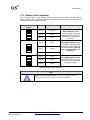
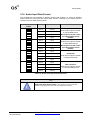
1
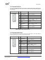
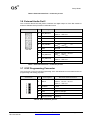
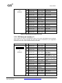
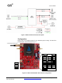
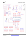
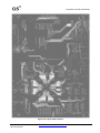
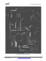
Q5E-UM-100A AUGUST-2006 Evaluation Board User Manual August 2006 ANAGRAM Technologies SA ZI Le Trési 6A 1028 Préverenges Switzerland Phone: + 41 21 804 1960 Fax: + 41 21 804 1961 [email protected] Abstract Q5 asynchronous sample rate converter evaluation board user manual. Copyright © Anagram Technologies SA All rights reserved. No part of this work covered by Anagram Technology SA copyright may be reproduced or copied in any form or by any means (graphic, electronic or mechanical, including photocopying, recording, taping or information retrieval systems) without the written permission of Anagram Technology SA. Submit Documentation Feedback Document Control Document History No. Primary Author(s) Description of Version Date Completed 100A TLn Initial revision 30-08-2005 Related Documentation Part Number Description Q5M-PB-100A Q5 product brief. Q5M-DS-100A Q5 evaluation board user manual. Ordering Information Part Number Description Package Q5M-PL-100A Asynchronous sample rate converter. Plastic Release Notice This document is under configuration control and updates will only be issued as a replacement document with a new version number. Q5E-UM-100A Q5 User Manual Submit Documentation Feedback Page 2 of 46 Preface Preface About This Manual This document provides the information needed to setup and operate the Q5 evaluation board. For a more detailed description of this product, please refer to the product data sheets available from the ANAGRAM Technologies web site at http://www.anagramtech.com. Support documents are listed in the section of this guide entitled Additional Documentation. Company Address ANAGRAM Technologies SA ZI Le Trési 6A 1028 Préverenges Switzerland Phone +41 21 804 1960 Fax +41 21 804 1961 Notice ANAGRAM Technologies S.A. provides the enclosed product(s) under the following conditions: This evaluation kit being sold by ANAGRAM Technologies is intended for use for ENGINEERING DEVELOPMENT OR EVALUATION PURPOSES ONLY and is not considered by ANAGRAM Technologies to be fit for commercial use. As such, the goods being provided may not be complete in terms of required design-, marketing-, and/or manufacturing-related protective considerations, including product safety measures typically found in the end product incorporating the goods. As a prototype, this product does not fall within the scope of the European Union directive on electromagnetic compatibility and therefore may not meet the technical requirements of the directive. Should this evaluation kit not meet the specifications indicated in the Evaluation Board User’s Guide, the kit may be returned within 30 days from the date of delivery for a full refund. THE FOREGOING WARRANTY IS THE EXCLUSIVE WARRANTY MADE BY SELLER TO BUYER AND IS IN LIEU OF ALL OTHER WARRANTIES, EXPRESSED, IMPLIED, OR STATUTORY, INCLUDING ANY WARRANTY OF MERCHANTABILITY OR FITNESS FOR ANY PARTICULAR PURPOSE. The user assumes all responsibility and liability for proper and safe handling of the goods. Further, the user indemnifies ANAGRAM Technologies from all claims arising from the handling or use of the goods. Please be aware that the products received may not be regulatory compliant or agency certified (FCC, UL, CE, etc.). Due to the open construction of the product, it is the user’s responsibility to take any and all appropriate precautions with regard to electrostatic discharge. EXCEPT TO THE EXTENT OF THE INDEMNITY SET FORTH ABOVE, NEITHER PARTY SHALL BE LIABLE TO THE OTHER FOR ANY INDIRECT, SPECIAL, INCIDENTAL, OR CONSEQUENTIAL DAMAGES. ANAGRAM Technologies currently deals with a variety of customers for products, and therefore our arrangement with the user is NOT EXCLUSIVE. ANAGRAM Technologies assumes NO LIABILITY FOR APPLICATIONS ASSISTANCE, CUSTOMER PRODUCT DESIGN, Q5E-UM-100A Q5 User Manual Submit Documentation Feedback Page 3 of 46 Preface SOFTWARE PERFORMANCE, OR INFRINGEMENT OF PATENTS OR SERVICES DESCRIBED HEREIN. Please read the Evaluation Board User’s Guide and, specifically, the Evaluation Board Warnings and Restrictions notice in the Evaluation Board User’s Guide prior to handling the product. This notice contains important safety information about temperatures and voltages. For further safety concerns, please contact the ANAGRAM Technologies customer support. Persons handling the product must have electronics training and observe good laboratory practice standards. No license is granted under any patent right or other intellectual property right of ANAGRAM Technologies covering or relating to any machine, process, or combination in which such ANAGRAM Technologies products or services might be or are used. Evaluation Board Warnings and Restrictions It is important to operate this Evaluation Board within the specified input and output ranges described in the Evaluation Board User’s Guide. Exceeding the specified input range may cause unexpected operation and/or irreversible damage to the Evaluation Board. If there are questions concerning the input range, please contact a ANAGRAM Technologies customer support prior to connecting the input power. Applying loads outside of the specified output range may result in unintended operation and/or possible permanent damage to the Evaluation Board. Please consult the Evaluation Board User’s Guide prior to connecting any load to the Evaluation Board output. If there is uncertainty as to the load specification, please contact ANAGRAM Technologies customer support. During normal operation, some circuit components may have case temperatures greater than 60C. The Evaluation Board is designed to operate properly with certain components above 60C as long as the input and output ranges are maintained. These components include but are not limited to linear regulators, switching transistors, digital to analog converters, and current sense resistors. These types of devices can be identified using the Evaluation Board schematic located in the Evaluation Board User’s Guide. When placing measurement probes near these devices during operation, please be aware that these devices may be very warm to the touch. How to Use This Manual Throughout this document, the abbreviation Q5-EVB and the term evaluation board are synonymous with the Q5 Module Evaluation Board. Chapter 1 provides an overview of the Q5-EVB block diagram and primary features are discussed. Chapter 2 provides general information regarding evaluation board handling and unpacking, absolute operating conditions, and the default switch and jumper configuration. Chapter 3 is the hardware setup guide for the evaluation board, providing all of the necessary information needed to configure the evaluation board switches and jumpers for product evaluation. Chapter 4 gives How-to instructions to perform advanced tasks with the Evaluation Board. Chapter 5 includes the evaluation board electrical schematic, PCB layout, and the Bill of Materials. Information About Cautions and Warnings Q5E-UM-100A Q5 User Manual Submit Documentation Feedback Page 4 of 46 Preface Note A NOTE provides additional or special information to assist operation. Disregarding a NOTE may cause inconvenience but will not result in personal injury or equipment damage. Caution A CAUTION is provided in a procedure whenever electrical or mechanical damage may occur. Failure to heed a CAUTION may result in some form of damage to the equipment; however, personal injury is unlikely. Additional Documentation The following documents provide information regarding selected non–ANAGRAM components, which are used in the assembly of the Evaluation Board. These documents are available from the corresponding manufacturers. Component Manufacturer CS8416 Cirrus Logic, http://www.cirrus.com DIT4192 Texas Instruments, http://www.ti.com PIC18F8722 Microchip, http://www.microchip.com GXO-U102 Golledge, http://www.golledge.com If You Need Assistance If you have questions regarding either the use of this evaluation board or the information contained in the accompanying documentation, please contact the ANAGRAM Technologies Customer Support +0041 (21) 804-1960 or visit the ANAGRAM Technologies web site at http://www.anagramtech.com. Repair and Maintenance Routine maintenance is not required. This product named as Q5 Module Evaluation Board is warranted to be free of any defect with respect to performance, quality, reliability and workmanship for a period of SIX (6) months from the date of shipment from ANAGRAM Technologies SA. In the event that your product proves to be defective in any way during this warranty period, we will gladly repair or replace this piece of equipment with a unit of equal or superior performance characteristics. Should you find this Q5 Module Evaluation Board has failed after your warranty period has expired, we will repair your defective piece of equipment for as long as suitable replacement component are available. You, the owner, will bear any labor/or component costs incurred in the repair or refurbishment of said equipment, beyond the SIX (6) months Q5E-UM-100A Q5 User Manual Submit Documentation Feedback Page 5 of 46 Preface warranty period. Any attempt to repair this product by anyone during this period other than rd by ANAGRAM Technologies SA or any authorized 3 party, will void your warranty. ANAGRAM Technologies SA reserves the right to assess any modifications or repairs made by you and decide if they fall within warranty limitations, should you decide to return your product for repair. In no event shall ANAGRAM Technologies SA be liable for direct, indirect, special, incidental, or consequential damages (including loss and profits) incurred by the use of this product. Implied warranties are expressly limited to the duration of this warranty. A Return Material Authorization Number (RMA) will be issued to you, as well, as specific shipping instructions, should you wish our factory to repair your Evaluation Board. A temporary replacement, if required, will be made available for a nominal charge. Any shipping costs incurred, will be the responsibility of the customer. All products shipped to you from ANAGRAM Technologies SA, will be shipped collect. Copyright © 2006 ANAGRAM Technologies SA. All right reserved Contents of this publication may be not reproduced in any form without the written permission of ANAGRAM Technologies SA. Reproduction and / or reverse engineering of copyrighted software is prohibited. Q5E-UM-100A Q5 User Manual Submit Documentation Feedback Page 6 of 46 Table of Contents LIST OF FIGURES ............................................................................................................ 9 LIST OF TABLES............................................................................................................ 10 1 INTRODUCTION....................................................................................................... 11 2 3 1.1 Evaluation Board Features ............................................................................................11 1.2 1.3 Functional Block Diagram ..............................................................................................11 Clock Synchronization ...................................................................................................12 1.4 Custom Digital Hardware Interface ................................................................................12 GETTING STARTED ................................................................................................ 14 2.1 Electrostatic Discharge Warning ....................................................................................14 2.2 Absolute Maximum Operating Conditions ......................................................................14 2.3 2.4 Unpacking the Evaluation Board....................................................................................14 Default Configuration .....................................................................................................15 SETUP GUIDE .......................................................................................................... 16 3.1 Connector Block Diagram ..............................................................................................16 3.2 Power Supply Configuration...........................................................................................17 3.3 S/PDIF Input and Output Connector ..............................................................................17 3.4 3.5 External Audio-In ...........................................................................................................18 External Audio-Out 1 .....................................................................................................18 3.6 External Audio-Out 2 .....................................................................................................19 3.7 ICSP Programming Connector.......................................................................................19 3.8 3.9 PIC External Interface 1.................................................................................................20 PIC External Interface 2.................................................................................................20 3.10 PIC External Interface 3.................................................................................................21 3.11 PIC External Interface 4.................................................................................................22 3.12 LED Definition................................................................................................................22 3.12.1 Assigned LED.........................................................................................................23 3.12.2 Programmable LED ................................................................................................23 3.13 Master Clock Selection ..................................................................................................24 3.14 Audio Input Data Format................................................................................................25 4 3.15 Audio Output Data Format & Frequency ........................................................................26 3.16 Q5 Module Configuration ...............................................................................................27 HOW-TO GUIDE ....................................................................................................... 29 4.1 Recommended Test Setup ............................................................................................29 4.2 Standard Q5 Module Setup ...........................................................................................30 4.2.1 Functional Mode .....................................................................................................30 Q5E-UM-100A Q5 User Manual Submit Documentation Feedback Page 7 of 46 4.2.2 Configuration ..........................................................................................................31 4.3 Connecting an external master clock .............................................................................32 4.3.1 Functional description.............................................................................................32 4.3.2 Configuration ..........................................................................................................33 4.4 Connecting an External PCM Audio Source...................................................................33 4.4.1 Functional mode .....................................................................................................33 Configuration ........................................................................................................................34 4.5 Connecting an External DSD Audio Source ...................................................................35 4.5.1 Functional mode .....................................................................................................35 Configuration ........................................................................................................................36 5 SCHEMATICS AND BILL OF MATERIALS ............................................................. 38 5.1 Physical Dimensions......................................................................................................38 5.2 Schematic......................................................................................................................38 5.3 Bill of Materials ..............................................................................................................45 Q5E-UM-100A Q5 User Manual Submit Documentation Feedback Page 8 of 46 List of Figures Figure 1: Q5-EVB functional block diagram..................................................................................12 Figure 2: Clock domain block diagram illustrating DSS™.............................................................12 Figure 3: Evaluation board with mayor components and connector locations...............................16 Figure 4: Test setup for performance measurement.....................................................................29 Figure 5: Test setup for audio listening. .......................................................................................30 Figure 6: Standard setup functional block diagram.......................................................................31 Figure 7: Standard hardware setting ............................................................................................31 Figure 8: External master clock functional description..................................................................32 Figure 9: External master clock board configuration.....................................................................33 Figure 11: External PCM Audio Source board configuration. .......................................................34 Figure 13: External DSD Audio Source board configuration.........................................................36 Figure 14: Evaluation board physical dimension. .........................................................................38 Figure 15: Digital Audio Schematics-1. ........................................................................................39 Figure 16: MCU & Clock circuitry schematics-2. ..........................................................................40 Figure 17: Power Supply schematics-3. .......................................................................................41 Figure 18: Layout Silk Screen schem-4........................................................................................42 Figure 19: Layout TOP schem-5. .................................................................................................43 Figure 20: Layout BOTTOM schem-6. .........................................................................................44 Figure 21: Evaluation board bill of materials.................................................................................46 Q5E-UM-100A Q5 User Manual Submit Documentation Feedback Page 9 of 46 List of Tables Table 1: Absolute maximum ratings. ............................................................................................14 Table 2: Evaluation board connector types. .................................................................................17 Table 3: S/PDIF input connector. .................................................................................................17 Table 4: S/PDIF output connector. ...............................................................................................17 Table 5: Digital input connector pin out. .......................................................................................18 Table 6: External Audio-Out 1 connector pin out. .........................................................................19 Table 7: External Audio-Out 1 connector pin out. .........................................................................19 Table 8: ICSP connector pin out. .................................................................................................19 Table 9: PIC External Connector 1 pin out. ..................................................................................20 Table 10: PIC External Connector 2 pin out. ................................................................................21 Table 11: PIC External Connector 3 pin out. ................................................................................22 Table 12: PIC External Connector 4 pin out. ................................................................................22 Table 13: Led definition 1st group. ................................................................................................23 Table 14: Led definition 2nd group. ...............................................................................................23 Table 15: Master clock selection. .................................................................................................24 Table 16: Audio input data format selections................................................................................25 Table 17: Audio output data format selections. ............................................................................26 Table 18: Audio output data frequency selections........................................................................26 Table 19: Word length selection...................................................................................................27 Table 20: Dither selection. ...........................................................................................................28 Table 21: Standard clock selection. .............................................................................................28 Table 22: OWW selection. ...........................................................................................................28 Q5E-UM-100A Q5 User Manual Submit Documentation Feedback Page 10 of 46 Introduction 1 Introduction This chapter gives a brief introduction to the features and principle technologies behind the Q5 Module Evaluation Board (Q5-EVB). 1.1 Evaluation Board Features The Q5-EVB is an all digital platform for testing and evaluating sample rate converters and upsamplers for consumer audio applications. Key features for the Q5-EVB include: 2-Channel digital audio input via CS8416 receiver. Audio extension connector supports asynchronous audio streams from USB, HDMI, or SACD in I2S or DSD formats Selection of master clock source, local 24.5760MHz oscillator or external clock via BNC connector. Dual digital output via DIT4196 transmitter and extension connector. Output formats: 48 to 192kHz I2S and 384kHz DSP mode. Complete board control over SPI bus with onboard PIC18F8722. User programmable LEDs and jumpers. Connector interface to all PIC18F8722 pins. 1.2 Functional Block Diagram The Q5-EVB is designed to function with ANAGRAM Technologies modules such as the Q5™ asynchronous sample rate converter. It features a digital receiver (CS8416) and transmitter (DIT4192) that provide digital audio input and output connectivity, as well as external connector for interfacing to your own digital source. The Q5-EVB functional block diagram, as shown in Figure 1, illustrates the main data flow between elements of the board. Digital input is handled by the CS8416 receiver which can receive and decode digital audio with sample rates up to 192kHz. Alternatively digital audio input can be supplied by an external connector, which bypasses the receiver and enters directly into the Q5 Module if required. This can, for example, be used to support asynchronous audio streams from USB or HDMI sources in I2S format or DSD signals from SACD sources. Digital output features the same architecture as the input, where by the DIT4192 transmitter can send and encode the digital audio via S/PDIF up to 192kHz. Alternatively the external connector allows the audio signals to be taken before the transmitter for interfacing directly to your custom digital hardware. Dual digital outputs allow the simultaneous driving of high performance 384kHz capable D/A converters in dual differential configuration, while at the same time providing an upsampled digital output for digital audio connectivity. Q5E-UM-100A Q5 User Manual Submit Documentation Feedback Page 11 of 46 Introduction Figure 1: Q5-EVB functional block diagram. 1.3 Clock Synchronization The Q5-EVB employs a concept of clock management called DSS™ synchronization which allows the system to handle a variety of sampling rates and data formats. DSS™ provides an elegant, cost effective, and future proof solution by synchronizing the complete audio system to a selectable clock source and unifying data to a single sampling rate as show in Figure 2. Figure 2: Clock domain block diagram illustrating DSS™. 1.4 Custom Digital Hardware Interface The Q5-EVB employs two digital audio ports that can be interfaced to custom digital audio hardware. In addition one of the ports interfaces directly to a digital transmitter up to 192kHz, the second is typically used to interface to high performance DACs operating at 384kHz. If you require interfacing to custom audio hardware either of these ports may be used. Q5E-UM-100A Q5 User Manual Submit Documentation Feedback Page 12 of 46 Introduction Note Philips I2S, Left-Justified, or Right-Justified audio formats do not support frequencies greater than 192kHz, to interface to a Q5 module port at greater than 192kHz please consult the appropriate data sheet of the Q5 module in question. Typically the format of 384kHz, for example, will correspond to that used by high performance DAC’s from Analog Devices, Wolfson Electronics, or TI / Burr Brown. Q5E-UM-100A Q5 User Manual Submit Documentation Feedback Page 13 of 46 Getting Started 2 Getting Started This chapter identifies important information regarding your Q5-EVB that you should know before getting your evaluation board up and running. 2.1 Electrostatic Discharge Warning Many of the components on the Q5-EVB are susceptible to damage by electrostatic discharge (ESD). Customers are advised to observe proper ESD handling precautions when unpacking and handling the Q5-EVB, including the use of a grounded wrist strap at an approved ESD workstation. Caution Failure to observe ESD handling procedures may result in damage to the evaluation board components. 2.2 Absolute Maximum Operating Conditions The user should be aware of the absolute maximum operating conditions for the Q5-EVB. Exceeding these conditions may result in damage to the Q5-EVB. Table 1 summarizes the critical data points. Parameter Maximum Condition Power Supply +9V 8V / 45 V Input S/PDIF 0.3 to 3.6V Input Digital Connector 0V to 3.6V Table 1: Absolute maximum ratings. Caution Failure to respect the Absolute Maximum Operating conditions may result in damage to the Q5-EVB components. 2.3 Unpacking the Evaluation Board Upon opening the Q5-EVB package, please check to make sure that the following items are included: Q5E-UM-100A Q5 User Manual Submit Documentation Feedback Page 14 of 46 Getting Started Q5 module evaluation development board (including Q5 module). International 9V power supply and outlet cable. CDROM containing source code of the microcontroller, user manual (this document) with complete schematics and BOM. If any of these items are missing, please contact the ANAGRAM Technologies Customer Support. 2.4 Default Configuration The factory default jumper settings result in the following Q5-EVB configuration: Operating with high quality local clock at 24.5760MHz. Input data format I2S. Output data format I2S. Word length output 24bit. Digital output via S/PDIF at 48kHz. Q5E-UM-100A Q5 User Manual Submit Documentation Feedback Page 15 of 46 Setup Guide 3 Setup Guide This chapter provides a step–by–step guide to configuring the Q5-EVB. Follow the sections to walk through the each connector setup. Please note that this section assumes the board is in its default factory configuration as described in Section 2.4. 3.1 Connector Block Diagram RX0-Port TX1-Port 1 2 1 2 DIGITAL MODULE 4 3 4 5 6 5 6 7 8 7 8 9 10 S/PDIF In 9 10 1 2 RCA S/PDIF In Audio-In CS8416 6 7 8 RCA S/PDIF Out S/PDIF Out Audio-Out Power Regulators ICSP Conn 59 57 55 53 NC 49 47 45 43 41 Clk3 Clk2 S 16 S 20 S 24 J7 PIC18F 8722 J9 J10 J11 2 4 6 8 10 12 14 16 18 20 1 3 5 7 9 Power 9V S 3 S 2 S 4 S 5 S 6 S 7 S 8 S 9 S 10 S 11 S 12 S 13 S 14 S 15 S 17 S 18 S 19 S 21 S 22 S 23 Module Config Jumpers Audio Data Format Jumpers 11 13 15 17 19 1 L L L L L L 1 2 3 4 5 6 Master Clock Jumpers 22 24 NC 28 30 NC 34 36 38 40 79 77 75 73 71 69 67 65 63 61 60 58 56 54 52 50 NC 46 44 42 21 23 NC 27 29 NC 33 35 37 39 J6 Clk3 4 5 TX0-Port 80 78 76 74 72 NC 68 66 64 62 Ext Clock 3 9 10 S1 Module Reset DIT4192 3 L L L L B D S 25 Programmable LEDs Figure 3: Evaluation board with mayor components and connector locations. Connector Q5E-UM-100A Q5 User Manual Name Connector Type Description RX0-PORT Ext Audio-In IDC Digital audio input TX1-PORT Ext Audio-Out 1 IDC Digital audio output TX0-PORT Ext Audio-Out 2 IDC Digital audio output Submit Documentation Feedback Page 16 of 46 Setup Guide J11 J10 J7 J9 ICSP CONN Audio-In Audio-Out PIC External Connector 1 PIC External Connector 2 PIC External Connector 3 PIC External Connector 4 PIC ISCP IDC PIC external interface IDC PIC external interface IDC PIC external interface IDC PIC external interface Barrette PIC programming connection S/PDIF Audio-In RCA Digital audio in via S/PDIF S/PDIF Audio-Out RCA Digital audio out via S/PDIF Table 2: Evaluation board connector types. 3.2 Power Supply Configuration The Q5-EVB is designed to function with digital only voltages and thus only requires a single +9.0V regulated DC power supply. The power supply is provided with your Q5-EVB, although the connecting cable may not be compatible with your local wall outlet. 3.3 S/PDIF Input and Output Connector The S/PDIF input is a 75-ohm coaxial cable (with signal levels of 0.5 volts) and RCA connectors. The minimal input level of S/PDIF interface is 200 mVpp, which allows for some cable losses. There is no real need for special quality cable as long as the cable is made of 75-ohm coaxial cable (a good video accessory cable works also as good S/PDIF cable). Connector Description Audio Signal RX Electrical Characteristics S/PDIF (0V +0.5V Digital signal input, 3.3V tolerant) S/PDIF Audio-In Table 3: S/PDIF input connector. Connector Description Audio Signal TX Electrical Characteristics SPDIF (0V +0.55V Digital signal output) S/PDIF Audio-Out Table 4: S/PDIF output connector. Note The S/PDIF signal is independent of polarity, which means that you do not have to concern with absolute polarity. Q5E-UM-100A Q5 User Manual Submit Documentation Feedback Page 17 of 46 Setup Guide 3.4 External Audio-In This connector allows the DM_EVB to process an external audio stream provided by any I2S PCM compatible audio source. This connector is also used for providing DSD signals to the Q5 module. Connector IDC 2x5 Pin Description Electrical Characteristics 1 RX0_BITCLK, DSD_ BITCLK VINHIGH = 2 VMIN – 5 VMAX VINLOW = 0.8 VMAX 2 GND Ground 3 GND Ground 4 GND Ground 5 RX_FSYNC VINHIGH = 2 VMIN – 5 VMAX VINLOW = 0.8 VMAX 6 GND Ground 7 GND GND 8 RX_SDATA1, DSD_L VINHIGH = 2 VMIN – 5 VMAX VINLOW = 0.8 VMAX 9 RX_SDATA2, DSD_R VINHIGH = 2 VMIN – 5 VMAX VINLOW = 0.8 VMAX 10 GND Ground Table 5: Digital input connector pin out. 3.5 External Audio-Out 1 This connector allows the DM_EVB to interface the digital output 1 of the Q5 module to another hardware board provided in I2S PCM audio format. Connector IDC 2x5 Q5E-UM-100A Q5 User Manual Pin Description Electrical Characteristics 1 TX0_BITCLK VINHIGH = 2 VMIN – 5 VMAX VINLOW = 0.8 VMAX 2 GND Ground 3 GND Ground 4 GND Ground 5 TX0_FSYNC VINHIGH = 2 VMIN – 5 VMAX VINLOW = 0.8 VMAX 6 GND Ground 7 GND GND 8 TX0_SDATA1 VINHIGH = 2 VMIN – 5 VMAX VINLOW = 0.8 VMAX 9 TX0_SDATA2 VINHIGH = 2 VMIN – 5 VMAX VINLOW = 0.8 VMAX 10 GND Ground Submit Documentation Feedback Page 18 of 46 Setup Guide Table 6: External Audio-Out 1 connector pin out. 3.6 External Audio-Out 2 This connector allows the DM_EVB to interface the digital output 2 of the Q5 module to another hardware board provided in I2S audio format. Connector IDC 2x5 Pin Description Electrical Characteristics 1 TX0_BITCLK VINHIGH = 2 VMIN – 5 VMAX VINLOW = 0.8 VMAX 2 GND Ground 3 GND Ground 4 GND Ground 5 TX0_FSYNC VINHIGH = 2 VMIN – 5 VMAX VINLOW = 0.8 VMAX 6 GND Ground 7 GND GND 8 TX0_SDATA1 VINHIGH = 2 VMIN – 5 VMAX VINLOW = 0.8 VMAX 9 TX0_SDATA2 VINHIGH = 2 VMIN – 5 VMAX VINLOW = 0.8 VMAX 10 GND Ground Table 7: External Audio-Out 1 connector pin out. 3.7 ICSP Programming Connector This connector is used for serial programming of the PIC18F8722 microcontroller and is for programming and testing purposes. Connector Pin Description Electrical Characteristics 1 MCLR Active Low VINHIGH = 2 VMIN – 5 VMAX VINLOW = 0.8 VMAX 2 POWER +3.3V 3 GND Ground 4 PGD ICSP™ data pin. 5 PGC ICSP™ clock pin. 6 Not Connected Floating Table 8: ICSP connector pin out. Q5E-UM-100A Q5 User Manual Submit Documentation Feedback Page 19 of 46 Setup Guide 3.8 PIC External Interface 1 This connector is used for accessing the pins 1-20 on the PIC18F8722 microcontroller. Some ports on the microcontroller are free and maybe customised to your application purposes, others are used to provide board functionality. Connector J11 IDC2x10 Pin Name Description Used By 1 MCU Pin 1 Port - RH2 LED_DSD_pin1 2 MCU Pin 2 Port - RH3 SW25_Pin2 3 MCU Pin 3 Port – RE1 SW23_Pin3 4 MCU Pin 4 Port – RE0 SW22_Pin4 5 MCU Pin 5 Port – RG0 6 MCU Pin 6 Port – RG1 7 MCU Pin 7 Port – RG2 8 MCU Pin 8 Port – RG3 9 MCU Pin 9 MCLR 10 MCU Pin 10 Port – RG4 11 Not Connected Floating 12 Not Connected Floating 13 MCU Pin 13 Port – RF7 SW21_Pin13 14 MCU Pin 14 Port – RF6 SW20_Pin14 15 MCU Pin 15 Port – RF5 SW18_Pin15 16 MCU Pin 16 Port – RF4 SW17_Pin16 17 MCU Pin 17 Port – RF3 SW15_Pin17 18 MCU Pin 18 Port – RF2 SW14_Pin18 19 MCU Pin 19 Port – RH7 SW13_Pin19 20 MCU Pin 20 Port – RH6 SW12_Pin20 ICSP Table 9: PIC External Connector 1 pin out. 3.9 PIC External Interface 2 This connector is used for accessing the pins 21-40 on the PIC18F8722 microcontroller. Some ports on the microcontroller are free and maybe customised to your application purposes, others are used to provide board functionality. Connector Q5E-UM-100A Q5 User Manual Pin Name Description Used By 21 MCU Pin 21 Port – RH5 SW11_Pin21 22 MCU Pin 22 Port – RH4 SW10_Pin22 23 MCU Pin 23 Port – RF1 SW9_Pin23 24 MCU Pin 24 Port – RF0 SW8_Pin24 25 Not Connected Floating 26 Not Connected Floating Submit Documentation Feedback Page 20 of 46 Setup Guide J10 IDC2x10 27 MCU Pin 27 Port – RA3 SW7_Pin27 28 MCU Pin 28 Port – RA2 SW6_Pin28 29 MCU Pin 29 Port – RA1 SW5_Pin29 30 MCU Pin 30 Port – RA0 SW4_Pin30 31 Not Connected Floating 32 Not Connected Floating 33 MCU Pin 33 Port – RA5 34 MCU Pin 34 Port – RA4 35 MCU Pin 35 Port – RC1 MD_CFG0 36 MCU Pin 36 Port – RC0 MD_CFG1 37 MCU Pin 37 Port – RC6 MD_CFG2 38 MCU Pin 38 Port – RC7 MD_CFG3 39 MCU Pin 39 Port – RJ4 SW2_Pin39 40 MCU Pin 40 Port – RJ5 SW3_Pin33 Table 10: PIC External Connector 2 pin out. 3.10 PIC External Interface 3 This connector is used for accessing the pins 41-60 on the PIC18F8722 microcontroller. Some ports on the microcontroller are free and maybe customised to your application purposes, others are used to provide board functionality. Connector J7 IDC2x10 Q5E-UM-100A Q5 User Manual Pin Name Description Used By 41 MCU Pin 41 Port – RJ6 42 MCU Pin 42 Port – RJ7 43 MCU Pin 43 Port – RC2 44 MCU Pin 44 Port – RC3 RX_SCLK, TX_SCLK, MD_SCLK 45 MCU Pin 45 Port – RC4 RX_ MISO, TX_MISO, MD_MISO 46 MCU Pin 46 Port – RC5 RX_ MOSI, TX_MOSI, MD_MOSI 47 MCU Pin 47 Port – RB7 ICSP 48 Not Connected Floating 49 MCU Pin 49 OSC1 50 MCU Pin 50 OSC2 51 Not Connected Floating 52 MCU Pin 52 Port – RB6 ICSP 53 MCU Pin 53 Port – RB5 RX_CS_B 54 MCU Pin 54 Port – RB4 MD_CS_B 55 MCU Pin 55 Port – RB3 TX_CS_B Submit Documentation Feedback MCU_CLK Page 21 of 46 Setup Guide 56 MCU Pin 56 Port – RB2 MD_IRQ_B 57 MCU Pin 57 Port – RB1 DBG_RX_GPO0 58 MCU Pin 58 Port – RB0 DBG_RX_GPO1 59 MCU Pin 59 Port – RJ3 BYP_CLK_CTRL 60 MCU Pin 60 Port – RJ2 TX_RST_B Table 11: PIC External Connector 3 pin out. 3.11 PIC External Interface 4 This connector is used for accessing the pins 61-80 on the PIC18F8722 microcontroller. Some ports on the microcontroller are free and maybe customised to your application purposes, others are used to provide board functionality. Connector J9 IDC2x10 Pin Name Description Used By 61 MCU Pin 61 Port – RJ1 MD_RST_B 62 MCU Pin 62 Port – RJ0 RX_RST_B 63 MCU Pin 63 Port – RD7 64 MCU Pin 64 Port – RD6 65 MCU Pin 65 Port – RD5 66 MCU Pin 66 Port – RD4 67 MCU Pin 67 Port – RD3 68 MCU Pin 68 Port – RD2 69 MCU Pin 69 Port – RD1 70 Not Connected Floating 71 Not Connected Floating 72 MCU Pin 72 Port – RD0 73 MCU Pin 73 Port – RE7 LED_LOCK_pin73 74 MCU Pin 74 Port – RE6 LED_BYP_pin74 75 MCU Pin 75 Port – RE5 LED_5_pin75 76 MCU Pin 76 Port – RE4 LED_6_pin76 77 MCU Pin 77 Port – RE3 LED_3_pin77 78 MCU Pin 78 Port – RE2 LED_4_pin78 79 MCU Pin 79 Port – RH0 LED_1_pin79 80 MCU Pin 80 Port – RH1 LED_2_pin80 Table 12: PIC External Connector 4 pin out. 3.12 LED Definition There are two groups of LEDs available on the Q5-EVB. The second group, on the right of the board, is assigned to specific functions while the other is programmable even though the first led on the left is assigned. Q5E-UM-100A Q5 User Manual Submit Documentation Feedback Page 22 of 46 Setup Guide 3.12.1 Assigned LED Led bunch LOCK BYP D11 D12 Number Description DSD D13 D11 ON = Receiver (CS8416) lock. D12 ON = Q5 module bypassed D13 ON = DSD input selected st Table 13: Led definition 1 group. 3.12.2 Programmable LED Led bunch Number Description LED1LED2LED3LED4LED5 LED6 D5 D6 D7 D8 D9 D10 D5 ON = Q5 module is connected D6 Programmable D7 Programmable D8 Programmable D9 Programmable D10 Programmable Table 14: Led definition 2 Q5E-UM-100A Q5 User Manual Submit Documentation Feedback nd group. Page 23 of 46 Setup Guide 3.13 Master Clock Selection The normal operation of the Q5-EVB requires that the master clock come from the on board oscillators of 24.5760MHz. Optionally and external master clock can be used from an external source via the BNC connector. Master Clock Jumper Number State SW16 SW16 Closed SW20 SW20 Open SW24 Open SW16 Open SW20 Closed SW24 Open SW16 SW16 Open SW20 SW20 Open SW24 Closed SW24 SW16 SW20 SW24 SW24 Mode External Master Clock The master clock for the Q5EVB will be sourced from an external clock via the BNC connector. 22.5792MHz Master Clock The master clock for the Q5EVB will be sourced from an on board oscillator. Warning this frequency is NOT yet supported. 24.5760MHz Master Clock The master clock for the Q5EVB will be sourced from an on board oscillator . Table 15: Master clock selection. Note Supported Clock Frequencies: The current version of the Q5 module only supports a master clock of 24.5760MHz Q5E-UM-100A Q5 User Manual Submit Documentation Feedback Page 24 of 46 Setup Guide 3.14 Audio Input Data Format The Q5-EVB has the possibility to interface with the Q5 module in a variety of standard audio formats for both input and output audio streams. Selection of the audio format is carried out by the audio format jumpers. Audio Input Data Jumper Number State Mode SW13 SW13 Closed SW17 SW17 Open SW21 SW21 Open SW25 SW25 Open Right Justified Audio stream input to module in right justified format. Warning this format is NOT yet supported by the Q5 module. SW13 SW13 Open SW17 SW17 Closed SW21 SW21 Open SW25 SW25 Open SW13 SW13 Open SW17 SW17 Open SW21 SW21 Closed SW25 SW25 Open SW13 SW13 Open SW17 SW17 Open SW21 SW21 Open SW25 SW25 Closed Left Justified Audio stream input to module in left justified format. Warning this format is NOT yet supported by the Q5 module. Philips I2S Audio stream input to module in Philips I2S format. DSD 2 Channel Audio stream input to module in 2 channel DSD format. Table 16: Audio input data format selections. Note Supported Input Data Formats: The current version of the Q5 module only supports stereo I2S and DSD data formats. Q5E-UM-100A Q5 User Manual Submit Documentation Feedback Page 25 of 46 Setup Guide 3.15 Audio Output Data Format & Frequency The output data format of the Q5 module supports three standard audio formats as well as three frequencies related to FS as described in Table 17: Audio output data format selections.. Audio Output Data Jumper Number State SW14 SW14 Closed SW18 SW18 Open SW22 SW22 Open SW14 Open SW18 Closed SW22 Open SW14 Open SW18 Open SW22 Closed SW14 SW18 SW22 SW14 SW18 SW22 Mode Philips I2S Audio stream output from module in Philips I2S format. Left Justified Audio stream output from module in left justified format. Warning this format is NOT yet supported by the Q5 module. Right Justified Audio stream output from module in right justified format. Warning this format is NOT yet supported by the Q5 module. Table 17: Audio output data format selections. Ratio Jumper Number State SW15 SW15 Closed SW19 SW19 Open SW23 SW23 Open SW15 SW15 Open SW19 SW19 Closed SW23 SW23 Open SW15 SW15 Open SW19 SW19 Open SW23 SW23 Closed Mode 1xFS Output on TX0-Port is at 1xFS sampling frequency. 2xFS Output on TX0-Port is at 2xFS sampling frequency. 4xFS Output on TX0-Port is at 4xFS sampling frequency. Table 18: Audio output data frequency selections. Q5E-UM-100A Q5 User Manual Submit Documentation Feedback Page 26 of 46 Setup Guide Note The ratio only applies to TX0-Port of the Q5 module. TX1-Port is configured according to the Q5 module data sheet. Note Supported Output Data Formats: The current version of the Q5 module only supports stereo I2S and DSP data formats. 3.16 Q5 Module Configuration All Q5 modules can be configured via the jumpers available on the Q5-EVB. Configuration includes setting the output performance settings such as dithering, output word length, including audio data formats as described in the previous sections, such settings are standard across all Q5 module versions. Output Word Length Jumper SW10 SW10 SW10 SW11 SW11 SW11 SW12 SW12 SW12 Number State Mode SW10 Closed SW11 Open SW12 Open 16bit Output Wordlength Output on TX0-Port from Q5 module is 16bit. SW10 Open SW11 Closed SW12 Open SW10 Open SW11 Open SW12 Closed 20bit Output Wordlength Output on TX0-Port from Q5 module is 20bit. 24bit Output Wordlength Output on TX0-Port from Q5 module is 24bit. Table 19: Word length selection. Note The output word length only applies to TX0-Port of the Q5 module. TX1-Port is configured according to the Q5 module data sheet. Q5E-UM-100A Q5 User Manual Submit Documentation Feedback Page 27 of 46 Setup Guide Dither Jumper SW 6 SW 9 SW 6 SW 9 Number State SW6 Open SW9 Open SW6 Open SW9 Closed Mode No Dither Applied Output on TX0-Port from Q5 module does not have dither applied. Trinangular PSD Dither Output on TX0-Port from Q5 module has triangular dither applied. Table 20: Dither selection. Ratio Jumper Number State Mode SW 4 SW4 Open SW 7 SW7 Open 1 Ratio Specifies a standard 24.5760MHz clock is used. SW4 Open SW7 Closed SW 4 SW 7 2 Ratio Specifies a standard 22.5792kHz clock is used. Warning this ratio is NOT yet supported by the Q5 module. Table 21: Standard clock selection. OWW jumper Number State Mode SW 5 SW5 Open SW 8 SW8 Open Not implemented. Reserved for futur use. Table 22: OWW selection. Note The clock ratio 2 is not yet supported by the Q5 module. Q5E-UM-100A Q5 User Manual Submit Documentation Feedback Page 28 of 46 How-to Guide 4 How-to Guide This chapter gives instructions on how to perform advanced tasks with the Q5-EVB. 4.1 Recommended Test Setup In order to be able to evaluate the performance of Q5 module, we suggest to set the Q5EVB according to ″Standard Q5 Module Setup″ (see §4.2 hereafter). It is recommended to wire the Q5-EVB as described in Figure 4 or Figure 5. Figure 4: Test setup for performance measurement. Q5E-UM-100A Q5 User Manual Submit Documentation Feedback Page 29 of 46 How-to Guide Figure 5: Test setup for audio listening. 4.2 Standard Q5 Module Setup 4.2.1 Functional Mode This is the standard mode with the default factory setting (default jumper setting see § 2.4 ). The audio signal is entered into the S/PDIF IN input connector to be decoded by the digital receiver (CS8416). The audio is then transmitted to the Q5 module according to the I2S stream. The Q5 module processes the audio data such that the output data is perfectly synchronized with the low jitter reference clock working at 24.5760MHz. The audio data generated by the Q5 module is in I2S format sampled at 24bit / 48kHz. Finally the digital transmitter (DIT4192) is switched ON and delivers an audio signal through the S/PDIF OUT connector. The block diagram hereafter shows the audio data flow. Q5E-UM-100A Q5 User Manual Submit Documentation Feedback Page 30 of 46 How-to Guide Figure 6: Standard setup functional block diagram. No signal of any kind has to be provided on the EXT DIGITAL IN. On the other hand, the DIGITAL OUT2 can be used to interface custom audio hardware like high performance DACs. The output data format is the same as the Q5 module output, namely, I2S format working on 24bit at 48kHz. 4.2.2 Configuration Please refer to the diagram below for the standard jumper setting SW 3 SW 2 SW 4 SW 5 SW 6 SW 7 SW 8 SW 9 SW10 SW11 SW12 SW16 SW13 SW14 SW15 SW20 SW17 SW18 SW19 SW24 SW21 SW22 SW23 SW25 Figure 7: Standard hardware setting The jumper setting is as following: SW 2 is ON: The S/PDIF Receiver is enabled. Q5E-UM-100A Q5 User Manual Submit Documentation Feedback Page 31 of 46 How-to Guide SW12 is ON: The word length outputs on TX0-port from Q5 module is 24bit. SW13 is ON: The audio stream input to Q5 module is Philips I2S format. SW14 is ON: The audio stream output from Q5 module is Philips I2S format. SW15 is ON: The sampling frequency ratio output from Q5 module is 1xFs. SW24 is ON: The master clock for Q5-EVB (DSS Synchronization system) is 24.5760MHz. All other jumpers are OFF (open) which results in the following: No dither applied. 24.5760MHz is the standard clock for the Q5 module. Q5 module not bypassed. 4.3 Connecting an external master clock 4.3.1 Functional description The Q5-EVB gives the possibility to connect an external master clock through the EXT-MCLK BNC, therefore the whole board will be driven using that clock including DSP, receiver, transmitter except the MCU which is always clocked by the onboard oscillator. Please note that the board can not be used as a master clock source using this BNC connection due to high performance one way buffers used. Currently the Q5 module only supports a 24.5760MHz clock source. In the block diagram hereafter, an example of configuration is presented where the whole board is clock by an external master clock. In that example, we enter the audio through the digital receiver and output through the digital transmitter but any other configuration is acceptable. Figure 8: External master clock functional description. Q5E-UM-100A Q5 User Manual Submit Documentation Feedback Page 32 of 46 How-to Guide 4.3.2 Configuration In order to make the Q5-EVB work correctly with an external master clock the external clock signal is supplied through the BNC connector call “EXT-MCLK” (see Figure 9: External master clock board configuration) and the corresponding jumpers must be correctly set. The impedance of the clock source cable has to be 75Ω. SW16 SW20 SW24 Figure 9: External master clock board configuration. SW16 is ON: The master clock for Q5-EVB (DSS Synchronization system) is supplied through the “EXT-MCLK” connector. All remaining jumpers can be configured according to the desired setting. 4.4 Connecting an External PCM Audio Source 4.4.1 Functional mode An external PCM audio data source can be directly connected to the Q5 module via the RX0 port. In this mode the digital receiver audio stream is disabled and the external data format is configured via the audio interface jumpers. The master clock can come from both, external or internal source. Q5E-UM-100A Q5 User Manual Submit Documentation Feedback Page 33 of 46 How-to Guide Figure 10 External PCM functional description. Configuration Please refer to the diagram below for the standard jumper setting. On the other hand, the RX0-Port pin description can be found in the § 3.4. External PCM Audio Source SW 3 SW 2 SW 4 SW 5 SW 6 SW 7 SW 8 SW 9 SW10 SW11 SW12 SW16 SW13 SW14 SW15 SW20 SW17 SW18 SW19 SW24 SW21 SW22 SW23 SW25 Figure 11: External PCM Audio Source board configuration. Q5E-UM-100A Q5 User Manual Submit Documentation Feedback Page 34 of 46 How-to Guide The jumper setting is as following: SW 2 is OFF: The S/PDIF Receiver is disabled. SW13 on: I2S input format selected. SW17, SW21, SW25 off. All remaining jumpers can be configured according to the desired setting. In the above example the configuration is as following: The audio stream output from Q5 module is Philips I2S format. The sampling frequency ratio output from Q5 module is 1xFs. No dither applied. The master clock for Q5-EVB (DSS Synchronization system) is 24.5760MHz. Caution DO NOT Plug connector on RX0-port before having removed jumper SW2. Otherwise electrical damage may occur. 4.5 Connecting an External DSD Audio Source 4.5.1 Functional mode The Q5 module accepts a Direct Stream Digital (DSD) audio stream at 2.8224MHz as input audio source. The Q5 Module converts the DSD data to PCM format using Anagram’s DSF™ Filtering, then standard PCM audio processing techniques are applied to the input audio. In DSD mode, the digital receiver audio stream is disabled. The master clock can come from both, external or internal source. Q5E-UM-100A Q5 User Manual Submit Documentation Feedback Page 35 of 46 How-to Guide Figure 12 External DSD functional description. Configuration Please refer to the diagram below for the standard jumper setting. The RX0-Port pin description can be found in the § 3.4. External DSD Audio Source SW 3 SW 2 SW 4 SW 5 SW 6 SW 7 SW 8 SW 9 SW10 SW11 SW12 SW16 SW13 SW14 SW15 SW20 SW17 SW18 SW19 SW24 SW21 SW22 SW23 SW25 Figure 13: External DSD Audio Source board configuration. Q5E-UM-100A Q5 User Manual Submit Documentation Feedback Page 36 of 46 How-to Guide The jumper setting is as following: SW2 is OFF: The S/PDIF Receiver is disabled. SW25: DSD input format selected. SW13, SW17, SW21 off. All remaining jumpers related to the master clock and to the output rate, format, dithering, word length, can be set as preferred. In the example of Figure 13, the settings selected are: The audio stream output from Q5 module is Philips I2S format. The sampling frequency ratio output from Q5 module is 1xFs. No dither applied. The master clock for Q5-EVB (DSS Synchronization system) is 24.5760MHz. Caution DO NOT Plug connector on RX0-port before having removed jumper SW2. Otherwise electrical damage may occur. Q5E-UM-100A Q5 User Manual Submit Documentation Feedback Page 37 of 46 Schematics and Bill of Materials 5 Schematics and Bill of Materials This chapter provides the electrical and physical layout information for the Q5-EVB. The bill of materials is included for component and manufacturer reference. 5.1 Physical Dimensions The Q5-EVB dimensions adhere to the standard European board size 127 x 180mm as shown in Figure 14: Evaluation board physical dimension. The maximum height of board with all components mounted is 32mm. 180 mm 170 mm (7086mil) (6692mil) Metal Coat PCB board 4mm/8mm 117mm (4606mil) 127mm (5000mil) Figure 14: Evaluation board physical dimension. 5.2 Schematic The complete electrical schematics of for the Q5-EVB are shown in Figure 15, Figure 16, Figure 17, and Figure 18 Q5E-UM-100A Q5 User Manual Submit Documentation Feedback Page 38 of 46 Schematics and Bill of Materials Figure 15: Digital Audio Schematics-1. Q5E-UM-100A Q5 User Manual Submit Documentation Feedback Page 39 of 46 Schematics and Bill of Materials Figure 16: MCU & Clock circuitry schematics-2. Q5E-UM-100A Q5 User Manual Submit Documentation Feedback Page 40 of 46 Schematics and Bill of Materials Figure 17: Power Supply schematics-3. Q5E-UM-100A Q5 User Manual Submit Documentation Feedback Page 41 of 46 Schematics and Bill of Materials Figure 18: Layout Silk Screen schem-4. Q5E-UM-100A Q5 User Manual Submit Documentation Feedback Page 42 of 46 Schematics and Bill of Materials Figure 19: Layout TOP schem-5. Q5E-UM-100A Q5 User Manual Submit Documentation Feedback Page 43 of 46 Schematics and Bill of Materials Figure 20: Layout BOTTOM schem-6. Q5E-UM-100A Q5 User Manual Submit Documentation Feedback Page 44 of 46 Schematics and Bill of Materials 5.3 Bill of Materials Item Quantity 1 17 Designator TAG C1,C2,C3,C4,C5,C6,C7,C8, Part Footprint Part ID 100nF SM/C_1206 76 SM/C_1206 80 C9,C10,C13,C14,C21,C22, C23,C28,C29 2 3 C11,C12,C19 10nF 3 4 C15,C16,C17,C20 470uF/50V low-ESR C_D13 274 4 1 C18 10uF/50V C_D5 72 5 4 C24,C25,C26,C27 10uF SM/C_1206 298 6 1 D1 10BQ040 SMD/D 237 7 10 D2,D5,D6,D7,D8,D9,D10, LED 1206 SM/C_1206 342 D11,D12,D13 8 1 D3 BAS16 SOT23_123 183 9 1 D4 MBR745 TO220AC 152 10 3 J1,J2,J4 IDC 2x5P IDC10P 10 11 2 J3,J5 RCA PCB RCA_PCB 339 12 1 J6 Barrette 6P M20_6P 16 13 4 J7,J9,J10,J11 IDC 2x10P IDC20P 279 14 1 J8 CONN BNC BNC 346 15 2 L2,L1 47uH SELF_D8 185 16 2 L3,L4 47uH SM/L_1812 66 17 1 MD1 Module BF532 MODULE_A 341 20 R1,R2,R3,R4,R10,R12,R23, 10K SM/R_1206 102 18 19 R25,R26,R27,R28,R29,R33, R34,R36,R40,R51,R52,R55, R56 20 1 R5 470R SM/R_1206 91 21 13 R6,R7,R8,R9,R13,R14,R15, 100R SM/R_1206 136 R16,R17,R18,R19,R20,R22 22 2 R24,R11 2K7 SM/R_1206 106 23 1 R21 300R SM/R_1206 92 24 13 R30,R31,R32,R38,R41,R42, 0R0 SM/R_1206 347 R43,R44,R45,R46,R47,R50, R54 25 1 R35 75R SM/R_1206 97 26 3 R37,R48,R57 1K SM/R_1206 95 27 1 R39 390R SM/R_1206 99 28 2 R49,R53 4x47R 1206_NETWORK 323 Q5E-UM-100A Q5 User Manual Submit Documentation Feedback Page 45 of 46 Schematics and Bill of Materials 29 21 R58,R59,R62,R63,R64,R65, 4K7 SM/R_1206 110 R66,R67,R68,R69,R70,R72, R73,R74,R84,R85,R86,R87, R88,R89,R90 30 1 R60 4x100R 1206_NETWORK 329 31 11 R61,R71,R75,R76,R77,R78, 47R SM/R_1206 93 R79,R80,R81,R82,R83 32 1 SW1 RESET SW SWITCH_FAV 258 33 24 SW2,SW3,SW4,SW5,SW6,SW7, Switch M20_2P 135 SW8,SW9,SW10,SW11,SW12, SW13,SW14,SW15,SW16,SW17, SW18,SW19,SW20,SW21,SW22, SW23,SW24,SW25 34 35 2 T2,T1 PULSE TRANSFO_PULSE 245 36 1 U1 DIT4192 SSOP28 41 37 1 U2 CS8416 TSSOP28 316 38 1 U3 LM2672M-5.0 SOIC8 271 39 1 U4 DC Jack DC JACK 277 40 1 U5 MAX4624 SOT23_6 348 41 1 U6 LM2676T-3.3 TO220-7 343 42 1 U7 74LCX244 TSSOP20 242 43 1 U8 PIC18F8722 TQFP80 282 44 1 Y1 24.5760MHz (3.3V) OSC14\4P 351 45 1 Y2 22.5792 MHz (3.3V) OSC14\4P 350 Figure 21: Evaluation board bill of materials. Q5E-UM-100A Q5 User Manual Submit Documentation Feedback Page 46 of 46


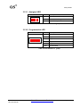
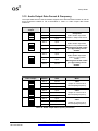


![Fio 2.0 UM ECU [ENG]](http://vs1.manualzilla.com/store/data/005638068_1-6dee15c8bb797972f1fa6aeeeee54189-150x150.png)