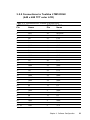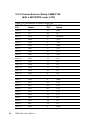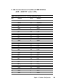
1
PCM-3346 Series
486 DX66-based Module with
SVGA/LCD/LAN Interface
User's Manual
Copyright notice
This document is copyright ©, 2000 and 2002, by Advantech Co., Ltd.
All rights are reserved. The original manufacturer reserves the right to
make improvements to the products described in this manual at any
time without notice.
No part of this manual may be reproduced, copied, translated or
transmitted in any form or by any means without the prior written
permission of the original manufacturer. Information provided in this
manual is intended to be accurate and reliable. However, the original
manufacturer assumes no responsibility for its use, nor for any
infringements upon the rights of third parties which may result from
its use.
Acknowledgements
AMD is a trademark of Advanced Micro Devices, Inc.
Award is a trademark of Award Software International, Inc.
Cyrix is a trademark of Cyrix Corporation.
IBM, PC/AT, PS/2 and VGA are trademarks of International Business
Machines Corporation.
Intel and Pentium are trademarks of Intel Corporation.
Microsoft Windows® is a registered trademark of Microsoft Corp.
RTL is a trademark of Realtek Semiconductor Co., Ltd.
C&T is a trademark of Chips and Technologies, Inc.
UMC is a trademark of United Microelectronics Corporation.
Winbond is a trademark of Winbond Electronics Corp.
STPC is a trademark of SGS Thomson Corp.
For more information on this and other Advantech products, please
visit our website at: http://www.advantech.com
For technical support and service, please visit our support website at:
http://www.advantech.com/support
This manual is for the PCM-3346, PCM-3346N, PCM-3346P,
PCM-3346F.
Part No. 2006334602
3rd Edition Printed in Taiwan Mar. 2002
Packing list
Before you begin installing your card, please make sure that the
following materials have been shipped:
• 1 PCM-3346 All-in-one single board computer
• 1 Start-up manual
• CD-ROM or Disks for utility, drivers, and manual (in PDF
format)
• 1 2.5" IDE flat cable, 44-pin to 44-pin
(product no. 1701440350)
• 1 keyboard / PS2 mouse cable
(product no. 1700060202)
• 2 serial port cables (product no. 1700100250)
• 1 parallel cable (product no. 1700260250)
• 1 26-34 pin FDD cable converter
(product no. 9681000044)
• 1 VGA cable (product no. 1701160150)
• 1 LAN cable (product no. 1701100202)
If any of these items are missing or damaged, contact your distributor
or sales representative immediately.
Contents
Chapter 1 General Information
1.1
1.2
1.3
1.4
Introduction ..........................................................................2
Features ...............................................................................3
Specifications ......................................................................4
1.3.1 Standard SBC functions ..............................................4
1.3.2 VGA function (PCM-3346F/P only) ..........................4
1.3.3 VGA function (PCM-3346/N only) ............................5
1.3.4 Ethernet function .........................................................5
1.3.5 Solid state disk ............................................................5
1.3.6 Mechanical and environmental ...................................5
Board dimensions ...............................................................6
CHAPTER 2 Installation
2.1
2.2
2.3
2.4
2.5
2.6
2.7
2.8
2.9
2.10
2.12
2.13
2.14
1
7
Connectors .........................................................................8
Locating connectors ...........................................................9
Safety precautions ............................................................11
Ethernet connector (CN1) (PCM-3346F/N only) ..........11
2.4.1 Ethernet connector (CN1) .........................................11
2.4.2 Network boot.............................................................11
LCD-A display connector (CN2) ....................................12
Serial ports (CN3, CN4)...................................................12
2.6.1 COM1 RS-232 port (CN3) ........................................12
2.6.2 COM2 RS-232 port (CN4) ........................................12
EIDE HDD connector (CN5) ...........................................13
2.7.1 Connecting the hard drive .........................................13
PC/104 connector (CN6) ..................................................13
Parallel port connector (CN7) .........................................14
Backlight connector (CN8) ..............................................14
VGA connector (CN9) .....................................................14
2.12.1 CRT display connector (CN9) ................................14
Reset button connector (CN10) .......................................14
Main power (+5 V / +12 V) connector (CN11) ..............15
2.15 PS/2 Keyboard/mouse connector (CN12) ......................15
2.16 5 V connector (CN13) ...................................................... 15
2.17 FDD connector (CN14) ....................................................16
2.17.1 Connecting the floppy drive....................................16
2.18 LCD-B connector (CN15) ................................................17
2.19 CompactFlash™ socket (CN16) ......................................17
2.20 SODIMM socket (Slot1) ..................................................18
2.20.1 Installing SODIMMs ..............................................18
CHAPTER 3 Software Configuration
3.1
3.2
3.3
Introduction ......................................................................20
Connections for four standard LCDs .............................20
3.2.1 Connections to Sharp LM64183P, LM64P89
(640 x 480 DSTN MONO LCD) ..................................20
3.2.2 Connections to Toshiba LTM10C042
(640 x 480 TFT color LCD)........................................... 21
3.2.3 Connections to Sharp LM64C142
(640 x 480 DSTN color LCD) .......................................22
3.2.4 Connections to Toshiba LTM12C275A
(800 x 600 TFT color LCD)........................................... 23
Ethernet software configuration .....................................24
CHAPTER 4 Award Bios Setup
4.1
4.2
19
25
System test and initialization .......................................... 26
4.1.1 System configuration verification .............................26
4.1.2 Further CMOS Data Safeguards ............................... 27
Award BIOS setup ...........................................................28
4.2.1 Entering setup ...........................................................28
4.2.2 Standard CMOS setup ...............................................29
4.2.3 Advanced CMOS setup .............................................30
4.2.4 Advanced chipset setup .............................................31
4.2.5 Power management setup .........................................32
4.2.6 PCI / Plug and Play configuration ............................33
4.2.7 Peripheral setup .........................................................34
4.2.8 Load BIOS defaults ...................................................35
4.2.9 Change password ......................................................36
4.2.10 Quit screen ..............................................................37
4.2.11 Save settings and exit ..............................................37
4.2.12 Exit without saving .................................................37
Chapter 5 SVGA Setup (for PCM-3346/N only)
5.1
5.2
5.3
39
Introduction ......................................................................40
5.1.1 Chipset ......................................................................40
5.1.2 Display memory ........................................................40
Installation of SVGA driver ............................................40
5.2.1 Installation for Windows 3.1 ....................................41
5.2.2 Installation for Windows 95 .....................................44
Further information.........................................................48
Chapter 6 PCI SVGA Setup (for PCM-3346F/P only) 49
6.1
6.2
6.3
Introduction ......................................................................50
6.1.1 Chipset ......................................................................50
6.1.2 Display memory ........................................................50
6.1.3 Display types .............................................................50
Installation of SVGA driver ............................................51
6.2.1 Installation for Windows 3.1 ....................................52
6.2.2 Installation for Windows 95 .....................................54
6.2.3 Installation for Windows NT ....................................57
Further information.........................................................60
Chapter 7 PCI Bus Ethernet Interface
(PCM-3346F/N only)
7.1
7.2
7.3
61
Introduction ......................................................................62
Installation of Ethernet driver ........................................62
7.2.1 Installation for MS-DOS and Windows 3.1 ..............62
7.2.2 Installation for Windows 95/98 ................................63
7.2.3 Installation for Windows NT ....................................65
Further information.........................................................67
Appendix A Programming the Watchdog Timer
A.1
Programming the watchdog timer .................................70
Appendix B Installing PC/104 Modules
B.1
91
System I/O ports ...............................................................92
DMA channel assignments ..............................................93
Interrupt assignments ...................................................... 93
1st MB memory map ....................................................... 94
Appendix E LCD Services
E.1
77
Ethernet connector (CN1) ...............................................78
LCD-A connector (CN2) ..................................................79
COM1 connector (CN3) ..................................................80
COM2 connector (CN4) ..................................................80
EIDE hard drive connector (CN5) .................................81
PC/104 connector (CN6) ..................................................82
Parallel port connector (CN7) .........................................82
Backlight connector (CN8) ..............................................83
VGA connector (CN9) .....................................................83
Reset button connector (CN10) .......................................84
Main power (+5 V) connector (CN11) ............................84
PS/2 keyboard/mouse connector (CN12) .......................85
5 V connector (CN13) ...................................................... 85
FDD connector (CN14) ....................................................86
LCD-B connector (CN15) ................................................87
CompactFlash™ socket (CN16) ......................................88
Appendix D System Assignments
D.1
D.2
D.3
D.4
73
Installing PC/104 modules ...............................................74
Appendix C Pin Assignments
C.1
C.2
C.3
C.4
C.5
C.6
C.7
C.8
C.9
C.10
C.11
C.12
C.13
C.14
C.15
C.16
69
95
LCD Services .................................................................... 96
Tables
Table 2-1: Connectors ..................................................................8
Table 2-2: Serial port default settings ......................................12
Table 3-1: Connections to Sharp LM64183P & LM64P89 ....20
Table 3-2: Connections to Toshiba LTM10DC042 .................21
Table 3-3: Connections to Sharp LM64C142 ..........................22
Table 3-4: Connections to Toshiba LTM12C2775A ...............23
Table B-1: PCM-3346 PC/104 connectors (CN12) ..................76
Table C-1: Ethernet connector (CN1) ......................................78
Table C-2: LCD-A connector (CN2) .........................................79
Table C-3: COM1 connector (CN3) .........................................80
Table C-4: COM2 connector (CN4) .........................................80
Table C-5: EIDE hard drive connector (CN5) ........................81
Table C-7: Parallel port connector (CN7)................................82
Table C-8: Backlight connector (CN8) .....................................83
Table C-9: VGA connector (CN9) ............................................83
Table C-10: Reset button connector (CN10) ............................84
Table C-11: Main power (+5 V) connector (CN11) .................84
Table C-12: PS/2 keyboard/mouse connector (CN12) ............85
Table C-13: 5 V connector (CN13) ...........................................85
Table C-14: FDD connector (CN14) .........................................86
Table C-15: LCD-B connector (CN15) .....................................87
Table C-16: CompactFlash™ socket (CN16) ...........................88
Table D-1: System I/O ports ......................................................92
Table D-2: DMA channel assignments .....................................93
Table D-3: Interrupt assignments .............................................93
Table D-4: 1st MB memory map ..............................................94
Figures
Figure 1-1: PCM-3346 dimensions .............................................6
Figure 2-1: Locating connectors (component side) ...................9
Figure 2-2: Locating connectors (solder side) .........................10
Figure 4-1: BIOS setup program initial screen .......................28
Figure 4-2: Standard CMOS setup screen ............................... 29
Figure 4-3: Advanced CMOS setup .......................................... 30
Figure 4-4: Advanced chipset setup .......................................... 31
Figure 4-5: Power management setup ......................................32
Figure 4-6: PCI / Plug and Play configuration ........................33
Figure 4-7: Peripheral setup...................................................... 34
Figure 4-8: BIOS setup program initial screen
Figure 4-9: BIOS setup program quit screen ..........................37
Figure B-1: PC/104 module mounting diagram ......................75
Figure B-2: PC/104 module dimensions (mm) (±0.1) ..............75
Figure C-1: CompactFlash™ socket ........................................89
CHAPTER
1
General Information
This chapter gives background information on the PCM-3346.
Sections include:
• Introduction
• Features
• Specifications
• Board dimensions
1.1
Introduction
The PCM-3346 is the ultimate cost-effective PC/104 solution for
limited-space applications. It offers all the functions of an
AT-compatible industrial computer on a single board, and occupies
less space than a 3½" hard drive. The PCM-3346 comes with an
embedded STPC Client processor on board. For maximum performance, the PCM-3346 also supports an EDO/FPM SODIMM socket
that can accept up to 64 MB memory.
Onboard features include a socket for a CompactFlash™ Card, 36-bit
interface, 100Base-T Ethernet, Enhanced IDE interface, one parallel
port, two serial ports (RS-232), a keyboard, and a PS/2 mouse
interface. A SVGA LCD display controller allows CRT resolutions up
to 1024 x 768 @ 64 K colors, LCD resolutions up to 1024 x 768 @ 64
K colors.
The PCM-3346 complies with the "Green Function" standard and
supports three types of power saving features: Normal, Doze, and
Sleep modes.
If you need any additional functions, the PCM-3346 has a PC/104
connector for future upgrades.
2
PCM-3346 User's Manual
1.2
Features
• Ultra-compact size single board computer, smaller than a 3½" hard
disk drive (96 mm x 90 mm)
• Onboard STPC Client CPU
• Up to 64 MB system memory, by way of SODIMM (EDO/FPM
DRAM)
• Onboard VGA/36-bit LCD interface
• Supports CompactFlash™ card
• Built-in Enhanced IDE (AT bus) hard disk drive interface
• Onboard PS/2 keyboard/mouse connector
• Two serial ports (RS-232)
• Upgradeable through PC/104 module
• Green engine with sleep mode and low power consumption
• +5 V power supply (for CPU board), +12 V power supply (for
PC/104, backlight)
• Onboard 10/100Base-T Ethernet interface
Chapter 1 General Information
3
1.3
Specifications
1.3.1 Standard SBC functions
• CPU: ST Thomson DX-66 STPC Client
• BIOS: Award 256 KB Flash BIOS, supports Plug & Play
• Fanless operation
• DRAM: One 144-pin 64-bit SODIMM socket supports 8/16/32/64
MB 3.3 V FPM / EDO SODIMM
• SSD: Supports one CompactFlash™ card
• Network: RTL 8139 chipset
• Watchdog :
1.6 sec interval watchdog timer (optional flexible interval available)
• IDE interface: One Enhanced IDE
• PC/104 expansion: 104-pin 16-bit PC/104 module connectors
1.3.2 VGA function (PCM-3346F/P only)
• Controller: C&T 69000, supports CRT and 36-bit LCD
• Display memory: 2 MB SDRAM built-in
• Display resolution:
1024 x 768 @ 16 bpp (CRT), 1024 x 768 @ 16 bpp (LCD)
Colors
Resolution
256
64 K
16 M
640 x 480
OK
OK
OK
800 x 600
OK
OK
OK
1024 x 768
OK
OK
NG
Resolution Map for PCM-3346 Series
4
PCM-3346 User's Manual
1.3.3 VGA function (PCM-3346/N only)
• Display memory: 512 KB ~ 4 MB share memory, set in BIOS
• Display type: Supports CRT
• CRT display mode: Non-interlaced CRT monitors resolutions up to
1280 x 1024 @ 24 bpp
1.3.4 Ethernet function
• Chipset: RTL 8139
• Ethernet interface:
PCI 10/100 Mbps Ethernet. IEEE 802.3u protocol compatible
• Connection: Onboard 10-pin 2 mm connector
• Boot ROM combined with BIOS
1.3.5 Solid state disk
• Supports CompactFlash™ cards
1.3.6 Mechanical and environmental
• Operating voltage: +5 V only
• Power consumption:
+5 V @ 1.5 A (typical) @ 486 66 MHz CPU +32 MB
• Size (L x W): 96 mm x 90 mm (3.77" x 3.54")
• Weight: 0.11 kg (0.24 lb)
• Operating temperature: 0 ~ 70° C (32 ~ 158° F)
Chapter 1 General Information
5
1.4
Board dimensions
Figure 1-1: PCM-3346 dimensions
6
PCM-3346 User's Manual
CHAPTER
2
Installation
This chapter tells how to set up the
PCM-3346 hardware. It includes instructions on setting jumpers and connecting
peripherals, switches and indicators. Make
sure you read all the safety precautions
before you begin the installation procedure.
2.1
Connectors
The board has a number of connectors that allow you to configure
your system to suit your application.
The tables below shows the function of each of the board's connectors:
Table 2-1: Connectors
8
Label
Function
CN1
Ethernet connector
CN2
LCD-A connector
CN3
COM1 connector
CN4
COM2 connector
CN5
EIDE HDD connector
CN6
PC/104 connector
CN7
Parallel port connector
CN8
Backlight connector
CN9
VGA connector
CN10
Reset button connector
CN11
Main power (+5 V) connector
CN12
PS/2 keyboard/mouse connector
CN13
5 V connector
CN14
FDD connector
CN15
LCD-B connector
CN16
CompactFlash™ socket
Slot 1
SODIMM socket
PCM-3346 User's Manual
2.2
Locating connectors
Warning:
Make sure you use the correct component side.
Improper installation can cause serious damage to
your hardware!
Figure 2-1: Locating connectors (component side)
Chapter 2 Installation
9
Figure 2-2: Locating connectors (solder side)
10
PCM-3346 User's Manual
2.3
Safety precautions
Warning! Always completely disconnect the power cord from
your board whenever you are working on it. Do not
make connections while the power is on, because
sensitive electronic components can be damaged by
a sudden rush of power.
Caution!
2.4
Always ground yourself to remove any static charge
before touching the board. Modern electronic
devices are very sensitive to static electric charges.
Use a grounding wrist strap at all times. Place all
electronic components on a static-dissipative
surface or in a static-shielded bag when they are not
in the chassis.
Ethernet connector (CN1)
(PCM-3346F/N only)
The PCM-3346F/N is equipped with a high performance 32-bit
PCI-bus Fast Ethernet interface which is fully compliant with IEEE
802.3u 100/10Base-T specifications. It is supported by all major
network operating systems.
The medium type can be configured via the RSet8139.EXE program
included on the utility disk. (See Chapter 5 for detailed information.)
2.4.1 Ethernet connector (CN1)
10/100Base-T connects to the PCM-3346F/N via an adapter cable to
the 10-pin 2 mm connector.
2.4.2 Network boot
The network boot feature is built into the BIOS. It can be enabled or
disabled in the chipset setup of the CMOS configuration. Refer to
"BIOS Setting" in Chapter 4 for more information.
Chapter 2 Installation
11
2.5
LCD-A display connector (CN2)
CN2 is a 40-pin dual-in-line header and is used to connect an LCD
display to the PCM-3346F/P.
2.6
Serial ports (CN3, CN4)
The PCM-3346 offers two serial ports, both RS-232. These ports
allow you to connect to any serial device (a mouse, printers, etc.) or
communication network.
2.6.1 COM1 RS-232 port (CN3)
The serial port connector's pin head housing is mounted on the bottom
edge of the card.
2.6.2 COM2 RS-232 port (CN4)
The secondary port, located above COM1, consists of a 10-pin,
dual-in-line pin head housing.
The IRQ and address range for both ports are fixed. However, if you
wish to disable the port or change these parameters later, you can do
this in the system BIOS setup. The table below shows the settings for
the PCM-3346 board's ports.
Table 2-2: Serial port default settings
Port
COM1
COM2
12
Address
3E8, 3F8
2E8, 2F8
PCM-3346 User's Manual
Interrupt
IRQ4
IRQ3
Default
3F8
2F8
2.7
EIDE HDD connector (CN5)
The built-in Enhanced IDE (Integrated Device Electronics) controller
supports up to two IDE devices, including CD-ROM drives, tape
backup drives, a large hard disk drive and other IDE devices.
2.7.1 Connecting the hard drive
Connecting drives is done in a daisy-chain fashion. It requires one or
two cables, depending on the drive size. All necessary cables are
included in your PCM-3346 package. 1.8" and 2.5" drives need a 1 x
44-pin to 2 x 44-pin flat-cable connector. 3.5" drives need a 1 x 44pin to 2 x 40-pin connector.
Wire number 1 on the cable is red or blue, and the other wires are
gray.
1. Connect one end of the cable to CN5. Make sure that the red (or
blue) wire corresponds to pin 1 on the connector, which is labeled
on the board (on the right side).
2. Plug the other end of the cable into the Enhanced IDE hard drive,
with pin 1 on the cable corresponding to pin 1 on the hard drive.
Unlike floppy drives, IDE hard drives can connect to either end of
the cable. If you install two drives, you will need to set one as the
master and one as the slave by using jumpers on the drives. If you
install just one drive, set it as the master.
2.8
PC/104 connector (CN6)
Refer to Appendix B in this manual.
Chapter 2 Installation
13
2.9
Parallel port connector (CN7)
Normally, the parallel port is used to connect the card to a printer. The
PCM-3346 includes a multi-mode (ECP/EPP/SPP) parallel port. It is
accessed via CN7, a 26-pin flat-cable connector.
You will need an adapter cable if you use a traditional DB-25 connector. The adpater cable should have a 26-pin connector on one end and
a DB-25 connector on the other.
The parallel port interrupt channel is designated as IRQ7.
2.10 Backlight connector (CN8)
The LCD inverter is connected to CN8 via a 4-pin connector to
provide +12 V power to the LCD display.
2.12 VGA connector (CN9)
The PCM-3346 board's SVGA interface can facilitate conventional
CRT displays. The card has a connector to support CRT VGA
monitors.
2.12.1 CRT display connector (CN9)
CN9 is a 16-pin, pin head housing connector. Please use the VGA
cable (provided with your kit) to convert the pin head housing
connector into a connector for conventional CRT displays.
Detailed information on pin assignments for CRT display connector
CN9 is given in Appendix C.
2.13 Reset button connector (CN10)
If you install a reset button, it should be a single pole switch rated at
5 V. Momentarily pressing the button will activate a reset.
For reset button pin assignments, please see Appendix C.
14
PCM-3346 User's Manual
2.14 Main power (+5 V / +12 V) connector
(CN11)
This supplies main power to the PCM-3346 (+5 V), and also 12 V
power to the backlight connector.
2.15 PS/2 Keyboard/mouse connector (CN12)
The PCM-3346 board provides a pin head keyboard connector, which
supports both a keyboard and a PS/2 style mouse. In most cases,
especially in embedded applications, a keyboard is not used. If the
keyboard is not present, the standard PC/AT BIOS will report an error
or failure during the power-on self test (POST) after resetting the PC.
The PCM-3346 board's BIOS standard setup menu allows you to
select "Absent/Present" for your keyboard under the Advanced CMOS
Setup section. This allows non-keyboard operation in embedded
system applications without the system halting during the POST.
When "PS/2 mouse support" is enabled, your PS/2 mouse is automatically detected by the system.
2.16 5 V connector (CN13)
The PCM-3346 is equipped with a low power dissipation STPC. With
only a heat sink, the PCM-3346 will operate normally at temperatures
up to 60° C. At temperatures above 60° C, a fan is recommended. A
CPU fan power supply connector is provided (+5 V input) in addition
to the CPU power supply.
This provides power supply to the optional CPU cooling fan. This
connector is only available when +5 V power is supplied to the board.
Warning!
Before making the connection, make sure that the
voltage is absolutely correct and matched with the
correct connector.
Chapter 2 Installation
15
2.17 FDD connector (CN14)
You can attach one 3.5" floppy drive to the the PCM-3346's onboard
controller. This is useful for notebooks, for example.
A daisy-chain drive cable converter (part no. 9681000044) is required
for a single floppy system. A 34-pin flat-cable connector is fitted on
one end of the cable converter, while the other end has one floppy
disk drive connector. It consists of a 34-pin flat-cable connector (for
the 3½” drives).
2.17.1 Connecting the floppy drive
1. Plug the 34-pin flat-cable connector into the cable converter. Make
sure that the red wire corresponds to pin 1 on the connector.
2. Attach the appropriate conector at the other end of the cable to the
floppy drive(s). You can use only one connector in the set. The set
at the other end (after the twist in the cable) connects to the A:
drive.
When connecting a 3½” floppy drive, you may have some difficulties
in determining which pin is number one. Look for a number on the
circuit board indicating pin number one. In addition, you should check
if the connector on the floppy drive has an extra slot. If the slot is up,
pin number one should be on the right. Please refer to any documentation that came with the drive for more information.
If your cable needs to be custom made, you can find the pin assignments for the board's connector in Appendix C.
2.18 LCD-B connector (CN15)
The PCM-3346F/P supports 36-bit LCD that must be connected to
both CN2 (40-pin) and CN15 (20-pin).
The pin assignments for both CN2 and CN15 can be found in
Appendix C.
16
PCM-3346 User's Manual
2.19 CompactFlash™ socket (CN16)
The PCM-3346 is equipped with a CompactFlash™ disk socket on the
solder side, which supports the IDE interface CompactFlash disk card.
The socket itself is specially designed to prevent any incorrect
installation of the CompactFlash disk card. When installing or
removing the CompactFlash disk card, please make sure that the
system power is off.
The CompactFlash™ disk card is defaulted as the E disk drive in your
PC system. The maximum capacity of Advantech's CFC is 128 MB.
To fit the Advantech CFC into the PCM-3346, simply plug it into the
designated connector. It will only fit when the red triangle on the CFC
is aligned with the triangle on the connector. The card will not fit any
other way (do NOT use excessive force).
2.20 SO DIMM socket (Slot1)
You can install anywhere from 8 MB to 128 MB of onboard SDRAM
memory using 8, 16, 32 or 128 MB 144-pin SODIMMs (Small Outline
Dual Inline Memory Modules).
2.20.1 Installing SODIMMs
Note:
The modules can only fit into a socket one way. Their
gold pins must point down into the SODIMM socket.
The procedure for installing SODIMMs appears below. Please follow
these steps carefully.
SO DIMM installation
1. Make sure that all power supplies to the system are switched off.
2. Install the SODIMM card. Install the SODIMM so that its gold pins
point down into the SODIMM socket.
3. Slip the SODIMM into the socket at a 45 degree angle and carefully
fit the bottom of the card against the connectors.
4. Gently push the SODIMM into a perpendicular position until the
Chapter 2 Installation
17
clips on the ends of the SODIMM sockets snap into place.
5. Check to ensure that the SODIMM is correctly seated and all
connector contacts touch. The SODIMM should not move around in
its socket.
Important: Only use standard form SODIMM memory modules
(as shown in the diagram below). Standardized
dimensions ensure a proper fit. Check with your
memory supplier about the SODIMM modules you will
use.
18
PCM-3346 User's Manual
CHAPTER
3
Software Configuration
This chapter details the software configuration information. It shows
you how to configure the card to match
your application requirements. Award
System BIOS is covered in Chapter 4.
Sections include:
• Introduction
• Connections for four standard LCDs
• Ethernet software configuration
3.1
Introduction
The PCM-3346 system BIOS and custom drivers are located in a 256
KB, 32-pin (JEDEC spec.) Flash ROM device, designated U18. A
single Flash chip holds the system BIOS, VGA BIOS and network
Boot ROM image. The display can be configured via CMOS settings.
This method minimizes the number of chips and difficulty of configuration. To set different types of LCD panels, please choose “panel
type” from the “integrated peripherals” menu in CMOS setup.
3.2
Connections for four standard LCDs
3.2.1 Connections to Sharp LM64183P, LM64P89
(640 x 480 DSTN MONO LCD)
Table 3-1: Connections to Sharp LM64183P & LM64P89
LM64183/64P89
Pin
Name
PCM-3346 CN2
Pin
Name
CN1-1
S
36
FLM
CN1-2
CP1
38
LP
CN1-3
CP2
35
SHFCLK
CN1-4
DISP
1
+5 V
CN1-5
VDD
2
+5 V
CN1-6
VSS
3
GND
CN1-7
VEE
-
External power*
CN1-8
DU0
12
P3
CN1-9
DU1
11
P2
P1
CN1-10
DU2
10
CN1-11
DU3
9
P0
CN1-12
DL0
16
P7
CN1-13
DL1
15
P6
CN1-14
DL2
14
P5
CN1-15
DL3
* LM64183P -17 V
Note:
20
13
LM64P89
P4
-20 V
Standard BIOS supports TFT and DSTN LCD
panels.
PCM-3346 User's Manual
3.2.2 Connections to Toshiba LTM10C042
(640 x 480 TFT color LCD)
Table 3-2: Connections to Toshiba LTM10DC042
LTM10C042
Pin
Name
PCM-3346 CN2
Pin
Name
1
GND
3
GND
2
CLK
35
SHFCLK
3
GND
4
GND
4
R0
27
P18
5
R1
28
P19
6
R2
29
P20
7
GND
8
GND
8
R3
30
P21
9
R4
31
P22
10
R5
32
P23
11
GND
33
GND
12
G0
19
P10
13
G1
20
P11
14
G2
21
P12
15
GND
33
GND
16
G3
22
P13
17
G4
23
P14
18
G5
24
P15
19
GND
34
GND
20
ENAB
37
M
21
GND
34
GND
22
B0
11
P2
23
B1
12
P3
24
B2
13
P4
25
GND
3
GND
26
B3
14
P5
27
B4
15
P6
28
B5
16
P7
29
GND
4
GND
30
VDD
1
+5 V
31, 32
VDD
2
+5 V
Chapter 3 Software Configuration
21
3.2.3 Connections to Sharp LM64C142
(640 x 480 DSTN color LCD)
Table 3-3: Connections to Sharp LM64C142
22
LM64C142
Pin
Name
PCM-3346 CN2
Pin
Name
CN1-1
YD
36
FLM
CN1-2
LP
38
LP
CN1-3
XCX
35
SHFCLK
CN1-4
DISP
1
+5 V
CN1-5
VDD
2
+5 V
CN1-6
VSS
3
GND
CN1-7
VEE
—
+27*
CN1-8
DU0
20
P11
CN1-9
DU1
19
P10
CN1-10
DU2
18
P9
CN1-11
DU3
17
P8
CN1-12
DU4
12
P3
CN1-13
DU5
11
P2
CN1-14
DU6
10
P1
CN1-15
DU7
9
P0
CN2-1
VSS
4
GND
CN2-2
DL0
24
P15
CN2-3
DL1
23
P14
CN2-4
DL2
22
P13
CN2-5
DL3
21
P12
CN2-6
DL4
16
P7
CN2-7
DL5
15
P6
CN2-8
DL6
14
P5
CN2-9
DL7
13
P4
CN2-10
VSS
8
GND
PCM-3346 User's Manual
3.2.4 Connections to Toshiba LTM12C275A
(800 x 600 TFT color LCD)
Table 3-4: Connections to Toshiba LTM12C2775A
LTM12C275A
Pin
Name
PCM-3346 CN2
Pin
Name
1
GND
3
GND
2
NCLK
35
SHFCLK
3
NC
-
NC
4
NC
-
NC
5
GND
4
GND
6
R0
27
P18
7
R1
28
P19
8
R2
29
P20
9
R3
30
P21
10
R4
31
P22
11
R5
32
P23
12
GND
8
GND
13
G0
19
P10
14
G1
20
P11
15
G2
21
P12
16
G3
22
P13
17
G4
23
P14
18
G5
24
P15
19
GND
33
GND
20
B0
11
P2
21
B1
12
P3
22
B2
13
P4
23
B3
14
P5
24
B4
15
P6
25
B5
16
P7
26
ENAB
37
M/DE
27
GND
34
GND
28
VCC
1
+5 V
29
VCC
2
+5 V
30
GND
3
GND
Chapter 3 Software Configuration
23
3.3
Ethernet software configuration
The PCM-3346’s onboard Ethernet interface supports all major
network operating systems. To configure the medium type, to view
the current configuration, or to run diagnostics, do the following:
1. Power the PCM-3346 on. Make sure that the RSET8139.EXE file
is located in the working drive.
2. At the prompt, type RSET8139.EXE and press <Enter>. The
Ethernet configuration program will then be displayed.
3. This simple screen shows all the available options for the Ethernet
interface. Just highlight the option you wish to change by using the
Up and Down keys. To change a selected item, press <Enter>, and
a screen will appear with the available options. Highlight your
option and press <Enter>. Each highlighted option has a helpful
message guide displayed at the bottom of the screen for additional
information.
4. After you have made your selections and are sure this is the
configuration you want, press ESC. A prompt will appear asking if
you want to save the configuration. Press Y if you want to save.
The Ethernet Setup Menu also offers three very useful diagnostic
functions. These are:
1. Run EEPROM Test
2. Run Diagnostics on Board
3. Run Diagnostics on Network
Each option has its own display screen that shows the format and
result of any diagnostic tests undertaken.
Note:
24
For Ethernet installation, please see Chapter 7.
PCM-3346 User's Manual
CHAPTER
4
Award BIOS Setup
This chapter describes how to set BIOS
configuration data.
4.1
System test and initialization
These routines test and initialize board hardware. If the routines
encounter an error during the tests, you will either hear a few short
beeps or see an error message on the screen. There are two kinds of
errors: fatal and non-fatal. The system can usually continue the bootup
sequence with non-fatal errors. Non-fatal error messages usually
appear on the screen along with the following instructions:
press <F1> to RESUME
Write down the message and press the F1 key to continue the bootup
sequence.
4.1.1 System configuration verification
These routines check the current system configuration against the
values stored in the board’s CMOS memory. If they do not match, the
program outputs an error message. You will then need to run the
BIOS setup program to set the configuration information in memory.
There are three situations in which you will need to change the CMOS
settings:
1. You are starting your system for the first time.
2. You have changed the hardware attached to your system.
3. The CMOS memory has lost power and the configuration information has been erased.
The PCM-3346’s CMOS memory has an integral lithium battery
backup. The battery backup should last at least five years in normal
service. When it finally runs down, you will need to replace the
complete unit.
26
PCM-3346 User's Manual
4.1.2 Further CMOS Data Safeguards
The PCM-3346 uses 2 additional functions that help ensure the
integrity of the CMOS memory data. A Batteryless CMOS bootup
function as well as automatic CMOS data refresh, are both utilized.
Both these functions rely on utilizing free space in the BIOS Flash
memory. Also, since the CMOS memory data and BIOS Flash saved
CMOS memory data are stored simultaneously, you are always
guaranteed an exact duplicate of the original CMOS memory data.
CMOS Data Backup
Because CMOS memory retention and integrity is especially critical
for normal startup, original CMOS memory values stored in the BIOS
Flash memory allow system boots to proceed normally. This is
especially critical in unmanned applications where system monitoring
is not convenient. This data redundancy (backup) combined with error
detecting capability make for more stable and reliable systems.
Batteryless Bootup
Since the BIOS Flash memory does not need a battery to retain its
contents (unlike the CMOS's lithium memory backup), and usually
has extra capacity, CMOS memory values are stored here. So, in the
event of CMOS backup battery failure and CMOS configuration
information being erased, when the start-up routine encounters a
CMOS memory error during bootup, CMOS configuration memory is
automatically transferred out of the BIOS Flash memory back into
CMOS memory. Hence, CMOS configuration information is replaced
with the original memory data and system bootup can then proceed
normally. This would reset the RTC, which is only a minor concern.
Chapter 4 Award BIOS Setup
27
4.2
Award BIOS setup
Award’s BIOS ROM has a built-in Setup program that allows users to
modify the basic system configuration. This type of information is
stored in battery-backed CMOS RAM, so that it retains the Setup
information when the power is turned off.
Please note that all PCI functions are not supported in this product.
4.2.1 Entering setup
Power on the computer and press <Del> immediately. This will allow
you to enter Setup.
Figure 4-1: BIOS setup program initial screen
28
PCM-3346 User's Manual
4.2.2 Standard CMOS setup
When you choose the Standard CMOS Setup option from the Award
BIOS Setup Utility menu, the screen shown below is displayed. This
standard setup menu allows users to configure system components
such as date, time, hard disk drive, floppy drive and display. Once a
field is highlighted, on-line help information is displayed at the
bottom left of the menu screen.
Figure 4-2: Standard CMOS setup screen
Chapter 4 Award BIOS Setup
29
4.2.3 Advanced CMOS setup
By choosing the Advanced CMOS Setup option from the
Award BIOS Setup Utility menu, the screen below is displayed. This
sample screen contains the manufacturer’s default values for the
PCM-3346.
Figure 4-3: Advanced CMOS setup
30
PCM-3346 User's Manual
4.2.4 Advanced chipset setup
By choosing the Advanced Chipset Setup option from the Award
BIOS Setup Utility menu, the screen below is displayed. This sample
screen contains the manufacturer’s default values for the PCM-3346.
Figure 4-4: Advanced chipset setup
Chapter 4 Award BIOS Setup
31
4.2.5 Power management setup
By choosing the Power Management Setup option from the Award
BIOS Setup Utility menu, the screen below is displayed. This sample
screen contains the manufacturer’s default values for the PCM-3346.
Figure 4-5: Power management setup
32
PCM-3346 User's Manual
4.2.6 PCI / Plug and Play configuration
By choosing the PCI / Plug and Play Setup option from the Award
BIOS Setup Utility menu, the screen below is displayed. This sample
screen contains the manufacturer’s default values for the PCM-3346.
Figure 4-6: PCI / Plug and Play configuration
Chapter 4 Award BIOS Setup
33
4.2.7 Peripheral setup
By choosing the Peripheral Setup option from the Award BIOS Setup
Utility menu, the screen below is displayed. This sample screen
contains the manufacturer’s default values for the PCM-3346.
Figure 4-7: Peripheral setup
34
PCM-3346 User's Manual
4.2.8 Load BIOS defaults
Auto Configuration loads the default system values directly from
ROM. If the stored record created by the setup program becomes
corrupted (and therefore unusable), these defaults will load automatically when you turn the PCM-3346 on. Two settings can be used here:
Fail-Safe or Optimized.
Confirm Password:
Figure 4-8: BIOS setup program initial screen
(showing Auto Configuration items)
Chapter 4 Award BIOS Setup
35
4.2.9 Change password
To change the password, choose the Set Password option form the
AWARD BIOS SETUP UTILITY menu, and press <Enter>.
1. If the CMOS is bad or this option has never been used, a default
password is stored in the ROM. The screen will display the
following message:
Enter Password:
Press <Enter>.
2. If the CMOS is good or this option has been used to change the
default password, the user is asked for the password stored in the
CMOS. The screen will display the following message:
Confirm Password:
Enter the current password and press <Enter>.
3. After pressing <Enter> (ROM password) or the current password
(user-defined), you can change the password stored in the CMOS.
The password can be at most eight (8) characters long.
Remember: To enable this feature, you must first select either Setup
or System in Change User Password.
36
PCM-3346 User's Manual
4.2.10 Quit screen
Figure 4-9: BIOS setup program quit screen
4.2.11 Save settings and exit
If you select this option and press <Enter>, the values entered in the
setup utilities will be recorded in the chipset’s CMOS memory. The
microprocessor will check this every time you turn your system on,
and compare this to what it finds as it checks the system. This record
is required for the system to operate.
4.2.12 Exit without saving
Selecting this option and pressing <Enter> lets you exit the Setup
program without recording any new values or changing old ones.
Chapter 4 Award BIOS Setup
37
38
PCM-3346 User's Manual
CHAPTER
5
SVGA Setup
(for PCM-3346/N only)
• Introduction
• Installation of SVGA driver
- for Windows 3.1
- for Windows 95
• Further information
5.1
Introduction
The PCM-3346/N has an on-board VGA interface. The specifications
and features are described as follows:
5.1.1 Chipset
The PCM-3346/N uses a SGS Thomson STPC for its SVGA controller, which supports conventional analog CRT monitors. In addition, it
also supports interlaced and non-interlaced analog monitors (color and
monochrome VGA) in high-resolution modes while maintaining
complete IBM VGA compatibility. Digital monitors (i.e. MDA, CGA,
and EGA) are NOT supported. Multiple frequency (multisync)
monitors are handled as if they were analog monitors.
5.1.2 Display memory
With 512 K ~ 4 MB share memory, the VGA controller can drive
CRT displays or color panel displays with resolutions up to 1024 x
768 at 64 K colors.
5.2
Installation of SVGA driver
Complete the following steps to install the SVGA driver. Follow those
procedures in the flow chart that apply to the operating system which
you are using within your PCM-3346/N.
Important: The following windows illustrations are examples
only. You must follow the flow chart instructions and
pay attention to the instructions which then appear
on your screen.
40
Note 1:
The CD-ROM drive is designated as "D" throughout
this chapter.
Note 2:
<Enter> means pressing the “Enter” key on the
keyboard.
PCM-3346 User's Manual
5.2.1 Installation for Windows 3.1
1.
a. Insert the CD/disk
into the CD-ROM/
FDD drive.
b. Select "Main" in
Program Manager.
c. Double click the
"Windows Setup" icon.
d. Select "Change System
Setting" in Options.
e. Select "Other display
(Requires disk from
OEM)" in display.
2.
a. Type in the path of
the VGA Win31 driver
(drive D:\).
3.
a. During the installation,
you can choose the
resolution and colors
you want to use.
b. Press "OK".
4.
a. Type in the path of
the Win31 source code.
b. Press "OK".
D:\PC104\3346\Video\Umavga\Win3 1
D:\PC104\3346\Video\Umavga\Win3 1
Chapter 5 SVGA Setup (for PCM-3346/N only)
41
5.
6.
7.
42
a. Type in the path of
Win31 VGA driver.
b. Press "OK".
a. Type in the path of
the Win31 source.
b. Press "OK" to finish.
a. When Windows
asks you to restart,
select "Continue".
PCM-3346 User's Manual
D:\PC104\3346\Video\Umavga\Win3 1\
D:\PC104\3346\Video\Umavga\Win3 1\
8.
a. Before you restart
Windows, insert the
following system.ini
file into the Windows
directory:
[display]
Redundancy = off
9.
a. Restart Windows.
END
Chapter 5 SVGA Setup (for PCM-3346/N only)
43
5.2.2 Installation for Windows 95
1.
2.
3.
4.
44
a. Select "Start" ,
"Settings" ,
"Control Panel" ,
"Display" ,
"Settings".
b. Press "Advanced
Properties".
a. Choose the
"Adapter" label.
b. Press the
"Change..."
button.
a. Press the "Have
Disk" button.
a. Insert the utility
disc into the
CD-ROM drive.
b. Type: D:\PC104\
3346\Video\
Umavga\Win95
c. Press "OK".
PCM-3346 User's Manual
D:\PC104\3346\Video\Umavga\Win95
5.
a. Select the
highlighted item.
b. Click the "OK"
button.
6.
a. SGS-Thomson
STPC appears in
the adapter label.
b. Click the "Apply"
button.
7.
a. Press "Yes" to
reboot.
8.
a. Repeat Step 1 on
the previous page
of this manual.
The "UMA config"
label appears in
"Display".
b. Adjust resolution
and color.
Chapter 5 SVGA Setup (for PCM-3346/N only)
45
9.
a. Click the "UMA
Config" label.
b. Adjust the refresh
rate and display[7]
type.
c. Press "OK" to exit.
10.
a. Press "Yes" to set
set the monitor type.
11.
a. Select "Standard",
"Super VGA 800
x 600", or "XGA".
b. Press the "OK"
button.
12.
a. Choose "Restart"
to reboot.
END
46
PCM-3346 User's Manual
Note:
You may find a "PCI Early non-VGA device" message in System Properties. This message merely
indicates a normal situation, and your system's
functionality remains unimpaired. Advantech will
further resolve the display of this message in the
near future.
Chapter 5 SVGA Setup (for PCM-3346/N only)
47
5.3
Further information
You can obtain further information about PCI/SVGA installation in
your PCM-3346, including driver updates, troubleshooting guides and
FAQ lists. Simply visit the following web resources:
Advantech websites: www.advantech.com
www.advantech.com/support
48
PCM-3346 User's Manual
CHAPTER
6
PCI SVGA Setup
(for PCM-3346F/P only)
• Introduction
• Installation of SVGA driver
- for Windows 3.1
- for Windows 95
- for Windows NT
• Further information
6.1
Introduction
The PCA-3346F/P has an onboard PCI flat panel/VGA interface. The
specifications and features are described as follows:
6.1.1 Chipset
The PCM-3346F/P uses a C&T 69000 chipset for its PCI/SVGA
controller. It supports many popular LCD, EL, and gas plasma flat
panel displays and conventional analog CRT monitors. The 69000
VGA BIOS supports monochrome LCD, EL, color TFT and STN
LCD flat panel displays. In addition, it also supports interlaced and
non-interlaced analog monitors (color and monochrome VGA) in
high-resolution modes while maintaining complete IBM VGA
compatibility. Digital monitors (i.e. MDA, CGA, and EGA) are NOT
supported. Multiple frequency (multisync) monitors are handled as if
they were analog monitors.
6.1.2 Display memory
With onboard 2 MB display memory, the VGA controller can drive
CRT displays or color panel displays with resolutions up to 1024 x
768 at 64 K colors.
6.1.3 Display types
CRT and panel displays can be used simultaneously. The
PCM-3346F/P can be set in one of three configurations: on a CRT, on
a flat panel display, or on both simultaneously. The system is initially
set to simultaneous display mode. The utility disks includes three
*.COM files in the subdirectory Utility\vga\ which can be used
to configure the display. In order to use these configuration programs,
type the file name and path at the DOS prompt.
CT.COM: Enables CRT display only
FP.COM: Enables panel display only
SM.COM: Enables both displays simultaneously
50
PCM-3346 User's Manual
6.2
Installation of SVGA driver
Complete the following steps to install the SVGA driver. Follow the
procedures in the flow chart that apply to the operating system that
you you are using within your PCA-3346F/P.
Important: The following windows illustrations are examples
only. You must follow the flow chart instructions and
pay attention to the instructions which then appear
on your screen.
Note 1:
The CD-ROM drive is designated as "D" throughout
this chapter.
Note 2:
<Enter> means pressing the “Enter” key on the
keyboard.
Chapter 6 PCI SVGA Setup (for PCM-3346F/P only)
51
6.2.1 Installation for Windows 3.1
1.
a. Insert the utility
disc into the
CD-ROM drive.
b. Select "File" in
Program Manager.
c. Click "Run" and
type: D:\PC104\
Video\69000\Win31
2.
a. Choose the
language you want
to use during
installation.
3.
a. Select the
highlighted item.
b. Press "ENTER".
4.
a. Press "ENTER" to
install all
resolutions.
52
PCM-3346 User's Manual
D:\PCI104\Video\69000\Win31
5.
a. Type the path of
the operating
system.
6.
a. When installation
is completed,
reboot the system.
b. You will see the
"ChipsCPL" icon in
the control panel.
7.
ChipsCPL
a. Double click
"ChipsCPL".
b. Adjust screen size,
color and refresh
rate to your
preferences.
END
Chapter 6 PCI SVGA Setup (for PCM-3346F/P only)
53
6.2.2 Installation for Windows 95
1.
a. Select "Start" ,
"Settings" ,
"Control Panel" ,
"Display" ,
"Settings".
b. Press "Advanced
Properties".
2.
a. Choose the
"Adapter" label.
b. Press the
"Change..."
button.
3.
a. Press the "Have
Disk" button.
4.
a. Insert the utility
disc into the
CD-ROM drive.
b. Type D:\PC104\
Video\69000\Win95
c. Press "OK".
54
PCM-3346 User's Manual
D:\PC104\Video\69000\Win95
5.
a. Select the
highlighted item.
b. Click the "OK"
button.
6.
a. C&T69000
appears in the
adapter label.
b. Click the "Apply"
button.
7.
a. Press "Yes" to
reboot.
8.
a. Repeat Step 1 on
the previous page
of this manual.
The "CHIPS"
label appears in
"Display".
b. Adjust resolution
and color.
69000
69000
Chapter 6 PCI SVGA Setup (for PCM-3346F/P only)
55
9.
a. Click the "CHIPS"
label.
b. Adjust the refresh
rate and display[7]
type.
c. Press "OK" to
exit.
10.
a. Press "Yes" to
set the monitor
type.
11.
a. Select
"Standard",
"Super VGA 800
x 600", or "XGA".
b. Press the "OK"
button.
12.
a. Choose "Restart"
to reboot.
END
56
PCM-3346 User's Manual
6.2.3 Installation for Windows NT
1.
a. Select "Start", "Settings",
"Control Panel".
b. Double click the "Display"
icon.
2.
a. Choose the "Settings" label.
b. Press the "Display Type"
button.
3.
a. Press the "Change..." button.
4.
a. Click the "Have Disk..."
button.
Chapter 6 PCI SVGA Setup (for PCM-3346F/P only)
57
5.
a. Insert the utility disc into
the CD-ROM drive.
b. Type: D:\PC104\3346\
Video\Winnt
c. Press the "OK" button.
D:\PC104\3346\Video\Winnt
6.
a. Select the highlighted
item.
b. Press the "OK" button.
7.
a. Press "Yes" to proceed.
8.
a. Press "OK" to reboot.
58
PCM-3346 User's Manual
9.
a. Repeat Step 1 in this
manual, to select the
"Settings" label.
b. Adjust resolution and color.
c. Click "Test" to see the
result.
d. Click "OK" to save the
setting.
END
Chapter 6 PCI SVGA Setup (for PCM-3346F/P only)
59
6.3
Further information
For further information about the PCI/SVGA installation in your
PCA-3346, including driver updates, troubleshooting guides and FAQ
lists, visit the following web resources:
C&T website: www.chips.com
Advantech websites: www.advantech.com
www.advantech.com/support
60
PCM-3346 User's Manual
CHAPTER
7
PCI Bus Ethernet
Interface (PCM-3346F/N
only)
This chapter provides information on
Ethernet configuration.
• Introduction
• Installation of Ethernet driver
- for MS-DOS and Windows 3.1
- for Windows 95/98
• Further information
7.1
Introduction
The PCM-3346F/N is equipped with a high performance 32-bit
Ethernet chipset which is fully compliant with IEEE 802.3 100 Mbps
CSMA/CD standards. It is supported by major network operating
systems. It is also both 100Base-T and 10Base-T compatible. The
medium type can be configured via the RSET8139.exe program
included on the utility disk.
The Ethernet port provides a 10-pin 2 mm connector on board. The
network boot feature can be utilized by incorporating the boot ROM
image files for the appropriate network operating system. The boot
ROM BIOS files are combined with system BIOS, which can be
enabled/disabled in the BIOS setup.
7.2
Installation of Ethernet driver
Before installing the Ethernet driver, note the procedures below. You
must know which operating system you are using in your PCM-3346,
and then refer to the corresponding installation flow chart. Then just
follow the steps described in the flow chart. You will quickly and
successfully complete the installation, even if you are not familiar
with instructions for MS-DOS or Windows.
Note:
The windows illustrations in this chapter are examples only. You must follow the flow chart instructions
and pay attention to the instructions which then
appear on your screen.
7.2.1 Installation for MS-DOS and Windows 3.1
If you want to set up your Ethernet connection under the MS-DOS or
Windows 3.1 environment, you should first check your server system
model. For example, MS-NT, IBM-LAN server, and so on.
Then choose the correct driver to install in your panel PC.
The installation procedures for various servers can be found on
CD-ROM. The file path is: D:PC104\3346\Ethernet\wfw311
62
PCM-3346 User's Manual
7.2.2 Installation for Windows 95/98
1.
a. Select "Start",
"Settings",
"Control Panel".
b. Double click
"Network".
2.
a. Click "Add" and
prepare to install
network functions.
3.
a. Select the
"Adapter" item to
add the Ethernet
card.
4.
a. Click "Have Disk"
to install the driver.
Chapter 7 PCI Bus Ethernet Interface
63
5.
a. Insert the CD
into the D:\ drive.
b. Type: D:\PC104\
3346\Ethernet\
Win95\
c. Click "OK".
6.
a. Choose the
"Realtek" item.
b. Click "OK".
7.
a. Make sure the
configurations of
relevant items are
set correctly.
b. Click "OK" to
reboot.
D:\PC104\3346\Ethernet\Win95\
END
Note:
64
The correct path for Windows 98 is:
D:\PC104\3346\Ethernet\Win98\
PCM-3346 User's Manual
7.2.3 Installation for Windows NT
1.
a. Select "Start",
"Settings",
"Control Panel".
b. Double click
"Network".
2.
a. Choose the
"Adapters" label.
b. Click the "Add"
button.
3.
a. Press "Have
Disk".
a. Insert the CD
into the D:\ drive.
4.
b. Type: D:\PC104\
3346\Ethernet\Winnt\
c. Click "OK".
D:\PC104\3346\Ethernet\Winnt\
Chapter 7 PCI Bus Ethernet Interface
65
5.
a. Choose the
"Realtek" item.
b. Click "OK".
6.
a. Make sure the
configurations of
relevant items are
set correctly.
b. Click "OK" to
reboot.
END
66
PCM-3346 User's Manual
7.3
Further information
Realtek website: www.realtek.com
Advantech websites: www.advantech.com
www.advantech.com/support
Chapter 7 PCI Bus Ethernet Interface
67
68
PCM-3346 User's Manual
APPENDIX
A
Programming the
Watchdog Timer
The PCM-3346 is equipped with a
watchdog timer that resets the CPU or
generates an interrupt if processing comes
to a standstill for any reason. This feature
ensures system reliability in industrial
standalone or unmanned
environments.
A.1 Programming the watchdog timer
The default configuration of the timer is enabled with system reset.
To enable the watchdog timer, you must make a program which
writes 1 to I/O port address 443 (hex) at regular intervals. The first
time your program reads the port, it enables the watchdog timer. After
that, your program must write 1 to port 443 at time intervals of less
than 1.6 seconds. Otherwise, the watchdog timer will activate and
reset the CPU. When you want to disable the watchdog timer, your
program should write 0 to port 443.
If CPU processing comes to a standstill because of EMI or a software
problem, your program's signals to I/O port address 443 of the timer
will be interrupted. The timer will then automatically reset the CPU,
and data processing will continue normally.
You must make your program so that it writes 1 to I/O port 443 at an
interval shorter than the timer's preset interval. The timer's intervals
have a tolerance of ± 30%, so you should program an instruction that
will refresh the timer about every second.
70
PCM-3346 User's Manual
The following example shows how you might program the watchdog
timer in BASIC:
10
REM
Watchdog timer example program
20
X=Out &H443,1 REM
watchdog
30
GOSUB 1000 REM
complete
40
X=Out &H443,1 REM
50
GOSUB 2000 REM
complete
60
X=Out &H443,0 REM
70
END
1000
REM
Enable and refresh the
Task #1, takes 1 second to
Refresh the watchdog
Task #2, takes 1 second to
Disable the watchdog
Subroutine #1, takes 1 second to complete
.
.
.
1070
RETURN
2000
REM
Subroutine #2, takes 1 second to complete
.
.
.
2090
RETURN
Appendix A Programming the Watchdog Timer
71
72
PCM-3346 User's Manual
APPENDIX
B
Installing PC/104
Modules
This appendix gives instructions for
installing PC/104 modules.
B.1
Installing PC/104 modules
The PCM-3346's PC/104 connectors give you the flexibility to attach
PC/104 modules.
Installing these modules on the PCM-3346 is quick and simple. The
following steps show how to mount the PC/104 modules:
1. Remove the PCM-3346 from your system paying particular
attention to the safety instructions already mentioned above.
2. Make any jumper or link changes required to the CPU card now.
Once the PC/104 module is mounted you may have difficulty in
accessing these.
3. Normal PC/104 modules have male connectors and mount directly
onto the main card. (Refer to the diagram on the following page.)
4. Mount the PC/104 module onto the CPU card by pressing the
module firmly but carefully onto the mounting connectors.
5. Secure the PC/104 module onto the CPU card using the four
mounting spacers and screws.
74
PCM-3346 User's Manual
P C /1 0 4
M o u n tin g S u p p o rt
M a le
F e m a le
P C / 1 0 4 m o d u le
P C M -3 3 4 6
Figure B-1: PC/104 module mounting diagram
8.9
95.9
90.8
82.5
φ 6.4
90.8
φ 3.2
5.1
5.1
0
5.1
0
85.1
90.2
Figure B-2: PC/104 module dimensions (mm) (±0.1)
Appendix B Installing PC/104 Modules
75
Table B-1: PCM-3346 PC/104 connectors (CN12)
Pin
Number
0
1
2
3
4
5
6
7
8
9
10
11
12
13
14
15
16
17
18
19
20
21
22
23
24
25
26
27
28
29
30
31
32
Signal (CN12)
Row A
Row B
—
—
IOCHCHK* 0 V
SD7
RESETDRV
SD6
+5 V
SD5
IRQ9
SD4
-5 V
SD3
DRQ2
SD2
-12 V
SD1
ENDXFR*
SD0
+12 V
IOCHRDY N/C
AEN
SMEMW*
SA19
SMEMR*
SA18
IOW*
SA17
IOR*
SA16
DACK3*
SA15
DRQ3
SA14
DACK1*
SA13
DRQ1
SA12
REFRESH*
SA11
SYSCLK
SA10
IRQ7
SA9
IRQ6
SA8
IRQ5
SA7
IRQ4
SA6
IRQ3
SA5
DACK2*
SA4
TC
SA3
BALE
SA2
+5 V
SA1
OSC
SA0
0V
0V
0V
* low active
76
PCM-3346 User's Manual
Signal (CN13)
Row C
Row D
0V
0V
SBHE*
MEMCS16*
LA23
IOCS16*
LA22
IRQ10
LA21
IRQ11
LA20
IRQ12
LA19
IRQ15
LA18
IRQ14
LA17
DACK0*
MEMR*
DRQ0
MEMW*
DACK5*
SD8
DRQ5
SD9
DACK6*
SD10
DRQ6
SD11
DACK7*
SD12
DRQ7
SD13
+5 V
SD14
MASTER*
SD15
0V
KEY
0V
—
—
—
—
—
—
—
—
—
—
—
—
—
—
—
—
—
—
—
—
—
—
—
—
—
—
APPENDIX
C
Pin Assignments
This appendix contains information of a
detailed or specialized nature. It includes:
• Ethernet connector
• LCD-A connector
• COM1 connector
• COM2 connector
• EIDE HDD connector
• PC/104 connector
• Parallel port connector
• Backlight connector
• VGA connector
• Reset button connector
• Main power (+5 V) connector
• PS/2 keyboard/mouse connector
• 5 V connector
• FDD connector
• LCD-B connector
• CompactFlash™ socket
C.1
Ethernet connector (CN1)
2 4
1
6 8 10
3 5 7
9
Table C-1: Ethernet connector (CN1)
78
Pin
Signal
Pin
Signal
1
Vcc (+5 V)
2
ACTLED-
3
RX+
4
RX-
5
LILED-
6
GND
7
NC
8
GND
9
TX+
10
TX-
PCM-3346 User's Manual
C.2
LCD-A connector (CN2)
1 3
37 39
2 4
38 40
Table C-2: LCD-A connector (CN2)
Pin
Signal
Pin
Signal
1
VDDSAFE +5 V
2
VDDSAFE +5 V
3
GND
4
GND
5
VDDSAFE +3.3 V
6
VDDSAFE +3.3 V
7
NC
8
GND
9
P0
10
P1
11
P2
12
P3
13
P4
14
P5
15
P6
16
P7
17
P8
18
P9
19
P10
20
P11
21
P12
22
P13
23
P14
24
P15
25
P16
26
P17
27
P18
28
P19
29
P20
30
P21
31
P22
32
P23
33
GND
34
GND
35
SHIFT CLOCK
36
FLM (FIRST LINE MARKER)
37
M (DISPLAY ENABLE) 38
LP (LATCH PULSE)
39
ENABKL
ENAVEE
Note:
40
The model number of the CN2 socket is
DF13A-40DP-1.25V (Hirose Electric Co., Ltd.)
Appendix C Pin Assignments
79
C.3
COM1 connector (CN3)
2 4
1
6 8 10
3 5 7
9
Table C-3: COM1 connector (CN3)
Pin
Signal
Pin
Signal
1
RLSD
2
DSR
3
RX
4
RTS
5
TX
6
CTS
7
DTR
8
RI
9
GND
10
NC
C.4
COM2 connector (CN4)
1
2
3
4
5
6
7
8
9
10
Table C-4: COM2 connector (CN4)
80
Pin
Signal
Pin
Signal
1
RLSD
2
DSR
3
RX
4
RTS
5
TX
6
CTS
7
DTR
8
RI
9
GND
10
NC
PCM-3346 User's Manual
C.5
EIDE hard drive connector (CN5)
Table C-5: EIDE hard drive connector (CN5)
Pin
Signal
Pin
Signal
1
RESET-
2
GND
3
D7
4
D8
1
2
5
D6
6
D9
3
4
7
D5
8
D10
9
D4
10
D11
11
D3
12
D12
13
D2
14
D13
15
D1
16
D14
17
D0
18
D15
19
GND
20
NC
21
DRQ
22
GND
23
IOW-
24
GND
25
IOR-
26
GND
27
IOCHRDY
28
GND
29
DACK-
30
GND
31
IRQ
32
NC
41
42
33
SA1
34
NC
43
44
35
SA 0
36
SA2
37
HDCS1-
38
HDCS3-
39
NC
40
GND
41
Vcc
42
Vcc
43
GND
44
NC
* low active
Appendix C Pin Assignments
81
C.6
PC/104 connector (CN6)
For details on PC/104 connectors, please refer to Appendix B.
C.7
Parallel port connector (CN7)
1
14
2
15
12
25
13
26
Table C-7: Parallel port connector (CN7)
Pin
Signal
Pin
Signal
1
*STROBE
14
AFD
2
PD0
15
ERROR
3
PD1
16
INIT
4
PD2
17
SLIN
5
PD3
18
GND
6
PD4
19
GND
7
PD5
20
GND
8
PD6
21
GND
9
PD7
22
GND
10
ACKNOWLEDGE
23
GND
11
BUSY
24
GND
12
PE (PAPER EMPTY)
25
GND
13
SLCT
26
N/C
* low active
82
PCM-3346 User's Manual
C.8
Backlight connector (CN8)
4
3
2
1
Table C-8: Backlight connector (CN8)
Pin
Signal
1
+12 V
2
GND
3
BACKLIGHT ENABLE
4
N/C
C.9
VGA connector (CN9)
1
2
3
4
13
14
15
16
Table A-11: VGA connector (CN11)
Pin
Signal
Pin
Signal
1
RED_OUT
2
VCC_VGA
3
GREEN_OUT
4
GND
5
BLUE-OUT
6
N/C
7
N/C
8
D2C_DATA
9
GND
10
HS
11
GND
12
VS
13
GND
14
D2C_CLOCK
15
GND
16
N/C
Appendix C Pin Assignments
83
C.10 Reset button connector (CN10)
2
1
Table C-10: Reset button connector (CN10)
Pin
Signal
1
*MASTER RESET
2
GND
* low active
C.11 Main power (+5 V) connector (CN11)
4
3
2
1
Table C-11: Main power (+5 V) connector (CN11)
84
Pin
Signal
1
Vcc (+5 V)
2
GND
3
GND
4
+12 V
PCM-3346 User's Manual
C.12 PS/2 keyboard/mouse connector (CN12)
6
5
4
3
2
1
Table C-12: PS/2 keyboard/mouse connector (CN12)
Pin
Signal
1
PS/2 KB CLOCK
2
PS/2 KB DATA
3
PS/2 MOUSE CLOCK
4
GND
5
Vcc
6
PS/2 MOUSE DATA
C.13 5 V connector (CN13)
1
2
Table C-13: 5 V connector (CN13)
Pin
Signal
1
Vcc (+5 V)
2
GND
Appendix C Pin Assignments
85
C.14 FDD connector (CN14)
Table C-14: FDD connector (CN14)
Pin
Signal
1
Vcc (5 V)
2
INDEX
3
Vcc (5 V)
4
DRIVE SELECT 0
5
Vcc (5 V)
6
DISK CHANGE
7
NC
8
NC (READY)
9
NC (HD OUT)
10
MOTOR ON
11
NC
12
DIRECTION SELECT
13
NC (1.6 MB IN)
14
STEP
15
GND
16
WRITE DATA
17
GND
18
WRITE GATE
19
GND
20
TRACK 00
21
GND
22
WRITE PROTECT
23
GND
24
READ DATA
25
GND
26
SIDE SELECT
* low active
86
PCM-3346 User's Manual
C.15 LCD-B connector (CN15)
1 3
17 19
2 4
18 20
Table C-15: LCD-B connector (CN15)
Pin
Signal
Pin
Signal
1
GND
2
GND
3
P24
4
P25
5
P26
6
P27
7
P28
8
P29
9
P30
10
P31
11
P32
12
P33
13
P34
14
P35
15
GND
16
GND
17
NC
18
NC
19
NC
20
NC
Note:
The model number of the CN15 socket is
DF13A-20DP-1.25V (Hirose Electric Co., Ltd.)
Appendix C Pin Assignments
87
C.16 CompactFlash™ socket (CN16)
Table C-16: CompactFlash™ socket (CN16)
Pin
Signal
Pin
Signal
1
GND
2
D03
3
D04
4
D05
5
D06
6
D07
7
*CS0
8
A10
9
*ATA SEL
10
A09
11
A08
12
A07
13
+5 V
14
A06
15
A05
16
A04
17
A03
18
A02
19
A01
20
A00
21
D00
22
D01
23
D02
24
*IOCS16
25
*CD2
26
*CD1
27
D11
28
D12
29
D13
30
D14
31
D15
32
*CS1
33
*VS1
34
*IORD
35
*IOWR
36
*WE
37
INTRQ
38
+5 V
39
*CSEL
40
*VS2
41
*RESER
42
IORDY
43
*INPACK
44
*REG
45
*DASP
46
*PDIAG
47
D08
48
D09
49
D10
50
GND
* low active
88
PCM-3346 User's Manual
Figure C-1: CompactFlash™ socket
Appendix C Pin Assignments
89
90
PCM-3346 User's Manual
APPENDIX
D
System Assignments
This appendix contains information of a
detailed or specialized nature. It includes:
• System I/O ports
• DMA channel assignments
• Interrupt assignments
• 1st MB memory map
D.1
System I/O ports
Table D-1: System I/O ports
Addr. range (Hex) Device
000-01F
DMA controller
020-021
Interrupt controller 1, master
022-023
Chipset address
040-05F
8254 timer
060-06F
8042 (keyboard controller)
070-07F
Real-time clock, non-maskable interrupt (NMI)
mask
080-09F
DMA page register
0A0-0BF
Interrupt controller 2
0C0-0DF
DMA controller
0F0
Clear math co-processor
0F1
Reset math co-processor
0F8-0FF
Math co-processor
1F0-1F8
Fixed disk
200-207
Game I/O
278-27F
Parallel printer port 2 (LPT 3)
2F8-2FF
Serial port 2
300-31F
Prototype card
360-36F
Reserved
378-37F
Parallel printer port 1 (LPT 2)
380-38F
SDLC, bisynchronous 2
3A0-3AF
Bisynchronous 1
3B0-3BF
Monochrome display and printer adapter (LPT1)
3C0-3CF
Reserved
3D0-3DF
Color/graphics monitor adapter
3F0-3F7
Diskette controller
3F8-3FF
Serial port 1
* PNP audio I/O map range from 220 ~ 250H (16 bytes)
MPU-401 select from 300 ~ 330H (2 bytes)
92
PCM-3346 User's Manual
D.2
DMA channel assignments
Table D-2: DMA channel assignments
Channel
0
1
2
3
4
5
6
7
Function
Available
Available
Floppy disk (8-bit transfer)
Available
Cascade for DMA controller 1
Available
Available
Available
* Audio DMA select 0, 1 or 3
D.3
Interrupt assignments
Table D-3: Interrupt assignments
Interrupt#
IRQ 0
IRQ 1
IRQ 2
IRQ 8
IRQ 9
IRQ 10
IRQ 11
IRQ 12
IRQ 13
IRQ 14
IRQ 15
IRQ 3
IRQ 4
IRQ 5
IRQ 6
IRQ 7
Interrupt source
Interval timer
Keyboard
Interrupt from controller 2 (cascade)
Real-time clock
Cascaded to INT 0A (IRQ 2)
Available
Available
PS/2 mouse (non-releasable)
INT from co-processor
Fixed disk controller (primary)
Fixed disk controller (secondary)
Serial communication port 2
Serial communication port 1
Parallel port 2
Diskette controller (FDC)
Parallel port 1 (print port)
* PNP audio IRQ select: 5, 7, 9 or 10
* Ethernet function is auto-sensing
Appendix D System Assignments
93
D.4
1st MB memory map
Table D-4: 1st MB memory map
94
Addr. range (Hex)
Device
F000h - FFFFh
System ROM
D000 - EFFFh
Expansion ROM
CC00 - CFFFh
Ethernet boot ROM
C000 - CBFFh
32/40/44 K VGA BIOS
B800h - BFFFh
CGA/EGA/VGA text
B000h - B7FFh
Unused
A000h - AFFFh
EGA/VGA graphics
0000h - 9FFFh
Base memory
PCM-3346 User's Manual
APPENDIX
E
LCD Services
This appendix contains information on
Advantech's LCD lighting services.
E.1
LCD Services
LCD screens are very popular on Advantech's CPU cards, Biscuit PCs
and POS series products. "Lighting" LCDs is virtually impossible
without technical expertise. Advantech provides LCD lighting and
integration services to assist our customers in setting up their systems.
Advantech's LCD lighting guide explains how to make connections
between LCD interfaces and LCD panels, as well as how to control
contrast, brightness, VEE source, LCD inverter and all other factors
that affect the successful installation of LCD panels.
The following information details our LCD lighting services:
a) This policy is only valid for Advantech products that include LCD
support
b) The customer should send the following LCD components for
service:
• DC-AC inverter and cable (i.e. connector with/without wires)
and data sheet
• LCD flat panel and cable (connector with/without wires) and
complete data sheet
c) Advantech will normally charge the customer a deposit. The
deposit will be refunded when servicing exceeds a minimum
volume
d) The customer must sign the agreement and fax it to us prior to
sending the LCD package. Advantech reserves the right to refuse
service if the customer cannot provide the required documents and
auxiliary parts
e) Advantech will supply a BIOS file and connection cable to the
customer upon completing the service
f) A minimum of seven working days is required for completion of
service, starting from receipt of the LCD package by Advantech
For TFT display support lists, see our website at:
http://www.advantech.com/support
Please contact our customer service department for more detailed
information and service files.
96
PCM-3346 User's Manual