1
Master’s Thesis
University of Applied Sciences Augsburg
Department of Computer Science
Embedded Systems Trace Solutions
Analysis and Implementation of Embedded Systems Trace Solutions
Submitted by Dominic Rath, summer semester 2007
Examiner: Prof. Dr. Hubert Högl
Examiner: Prof. Burkhard Stork
Master’s Thesis
University of Applied Sciences Augsburg
Department of Computer Science
I affirm that the master’s thesis is my own work, and that it has never been submitted for
examination purposes before. All sources and citations used have been quoted as such, and all
utilized tools have been mentioned.
Dominic Rath
Embedded Systems Trace Solutions
Analysis of embedded systems trace solutions and prototype trace
implementations for ARM7, ARM9 and XScale based microcontrollers
Dominic Rath
c 2007 Dominic Rath
All rights reserved
12 11 10 09 08 07
First edition:
543210
27 September 2007
Permission is granted to copy, distribute and/or modify this document under the terms of the GNU Free Documentation License,
Version 1.2 or any later version published by the Free Software Foundation; with no Invariant Sections, no Front-Cover Texts,
and no Back-Cover Texts. A copy of the license is included in the section entitled "GNU Free Documentation License".
Contents
Contents
i
List of Figures
iv
List of Tables
v
1
Preface
1.1 Aim . . . . . . . . . . . . . . . . . . . . . . . . . . . . . . . . . . . . . . . . . . . . .
1.2 Conventions . . . . . . . . . . . . . . . . . . . . . . . . . . . . . . . . . . . . . . . . .
1.3 Prerequisite Knowledge . . . . . . . . . . . . . . . . . . . . . . . . . . . . . . . . . . .
1
1
1
2
2
Debugging Techniques
2.1 Static Analysis . . .
Compiler Warnings .
Static Analysis Tools
2.2 Debug Output . . . .
2.3 Start/Stop Debugging
2.4 Trace . . . . . . . .
3
4
.
.
.
.
.
.
.
.
.
.
.
.
.
.
.
.
.
.
.
.
.
.
.
.
.
.
.
.
.
.
.
.
.
.
.
.
.
.
.
.
.
.
.
.
.
.
.
.
.
.
.
.
.
.
.
.
.
.
.
.
.
.
.
.
.
.
.
.
.
.
.
.
.
.
.
.
.
.
.
.
.
.
.
.
.
.
.
.
.
.
.
.
.
.
.
.
.
.
.
.
.
.
.
.
.
.
.
.
.
.
.
.
.
.
.
.
.
.
.
.
.
.
.
.
.
.
.
.
.
.
.
.
.
.
.
.
.
.
.
.
.
.
.
.
.
.
.
.
.
.
.
.
.
.
.
.
.
.
.
.
.
.
.
.
.
.
.
.
.
.
.
.
.
.
.
.
.
.
.
.
.
.
.
.
.
.
.
.
.
.
.
.
.
.
.
.
.
.
.
.
.
.
.
.
.
.
.
.
.
.
3
3
3
4
4
5
6
Debugging Implementations
3.1 In-Circuit Emulators . .
3.2 Debug Monitors . . . . .
3.3 On-Chip Debugging . . .
3.4 Software Trace . . . . .
3.5 Hardware Trace Support
Bus Trace . . . . . . . .
Dedicated Trace Port . .
On-Chip Trace . . . . .
.
.
.
.
.
.
.
.
.
.
.
.
.
.
.
.
.
.
.
.
.
.
.
.
.
.
.
.
.
.
.
.
.
.
.
.
.
.
.
.
.
.
.
.
.
.
.
.
.
.
.
.
.
.
.
.
.
.
.
.
.
.
.
.
.
.
.
.
.
.
.
.
.
.
.
.
.
.
.
.
.
.
.
.
.
.
.
.
.
.
.
.
.
.
.
.
.
.
.
.
.
.
.
.
.
.
.
.
.
.
.
.
.
.
.
.
.
.
.
.
.
.
.
.
.
.
.
.
.
.
.
.
.
.
.
.
.
.
.
.
.
.
.
.
.
.
.
.
.
.
.
.
.
.
.
.
.
.
.
.
.
.
.
.
.
.
.
.
.
.
.
.
.
.
.
.
.
.
.
.
.
.
.
.
.
.
.
.
.
.
.
.
.
.
.
.
.
.
.
.
.
.
.
.
.
.
.
.
.
.
.
.
.
.
.
.
.
.
.
.
.
.
.
.
.
.
.
.
.
.
.
.
.
.
.
.
.
.
.
.
.
.
.
.
.
.
.
.
.
.
.
.
.
.
.
.
.
.
.
.
.
.
.
.
.
.
.
.
.
.
.
.
7
7
7
8
9
9
9
9
10
ARM
4.1 Architecture . . . . .
Programmer’s Model
4.2 Implementations . .
ARM7 . . . . . . . .
ARM9(E) . . . . . .
XScale . . . . . . . .
.
.
.
.
.
.
.
.
.
.
.
.
.
.
.
.
.
.
.
.
.
.
.
.
.
.
.
.
.
.
.
.
.
.
.
.
.
.
.
.
.
.
.
.
.
.
.
.
.
.
.
.
.
.
.
.
.
.
.
.
.
.
.
.
.
.
.
.
.
.
.
.
.
.
.
.
.
.
.
.
.
.
.
.
.
.
.
.
.
.
.
.
.
.
.
.
.
.
.
.
.
.
.
.
.
.
.
.
.
.
.
.
.
.
.
.
.
.
.
.
.
.
.
.
.
.
.
.
.
.
.
.
.
.
.
.
.
.
.
.
.
.
.
.
.
.
.
.
.
.
.
.
.
.
.
.
.
.
.
.
.
.
.
.
.
.
.
.
.
.
.
.
.
.
.
.
.
.
.
.
.
.
.
.
.
.
.
.
.
.
.
.
.
.
.
.
.
.
.
.
.
.
.
.
11
11
11
12
13
13
14
.
.
.
.
.
.
.
.
.
.
.
.
.
.
.
.
.
.
i
CONTENTS
ii
5
OpenOCD
5.1 Current State . . . . . . . . . . . . . . . . . . . . . . . . . . . . . . . . . . . . . . . .
5.2 Further Development . . . . . . . . . . . . . . . . . . . . . . . . . . . . . . . . . . . .
15
15
17
6
DCC Software Trace
6.1 DCC Registers . . . . . . . . . . . . . . . . . .
6.2 Accessing The DCC . . . . . . . . . . . . . . .
Core Access To DCC . . . . . . . . . . . . . . .
JTAG Access To DCC . . . . . . . . . . . . . .
6.3 OpenOCD Target Request Implementation . . . .
Target Request Protocol . . . . . . . . . . . . . .
ARM7/9 Target Request Code . . . . . . . . . .
6.4 OpenOCD DCC Software Trace Implementation
6.5 OpenOCD Target Request Usage . . . . . . . . .
6.6 OpenOCD Software Trace Usage . . . . . . . . .
6.7 ARM7/9 Target Request Constraints . . . . . . .
.
.
.
.
.
.
.
.
.
.
.
.
.
.
.
.
.
.
.
.
.
.
.
.
.
.
.
.
.
.
.
.
.
.
.
.
.
.
.
.
.
.
.
.
.
.
.
.
.
.
.
.
.
.
.
.
.
.
.
.
.
.
.
.
.
.
.
.
.
.
.
.
.
.
.
.
.
.
.
.
.
.
.
.
.
.
.
.
.
.
.
.
.
.
.
.
.
.
.
.
.
.
.
.
.
.
.
.
.
.
.
.
.
.
.
.
.
.
.
.
.
.
.
.
.
.
.
.
.
.
.
.
.
.
.
.
.
.
.
.
.
.
.
.
.
.
.
.
.
.
.
.
.
.
.
.
.
.
.
.
.
.
.
.
.
.
.
.
.
.
.
.
.
.
.
.
.
.
.
.
.
.
.
.
.
.
.
.
.
.
.
.
.
.
.
.
.
.
.
.
.
.
.
.
.
.
.
.
.
.
.
.
.
.
.
.
.
.
.
.
.
.
.
.
.
.
.
.
.
.
.
18
18
19
19
19
19
20
20
22
23
23
24
XScale On-Chip Trace
7.1 XScale Debugging . . . . . . . . . . . .
Mini ICache . . . . . . . . . . . . . . . .
OpenOCD XScale Debug Handler . . . .
7.2 Trace Message Format . . . . . . . . . .
7.3 OpenOCD XScale Trace Implementation
7.4 OpenOCD XScale Trace Usage . . . . . .
.
.
.
.
.
.
.
.
.
.
.
.
.
.
.
.
.
.
.
.
.
.
.
.
.
.
.
.
.
.
.
.
.
.
.
.
.
.
.
.
.
.
.
.
.
.
.
.
.
.
.
.
.
.
.
.
.
.
.
.
.
.
.
.
.
.
.
.
.
.
.
.
.
.
.
.
.
.
.
.
.
.
.
.
.
.
.
.
.
.
.
.
.
.
.
.
.
.
.
.
.
.
.
.
.
.
.
.
.
.
.
.
.
.
.
.
.
.
.
.
.
.
.
.
.
.
26
26
27
27
28
31
33
.
.
.
.
.
.
.
.
.
.
.
.
.
.
.
34
35
35
36
36
36
38
40
41
42
42
43
44
47
52
55
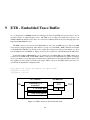
ETB - Embedded Trace Buffer
9.1 ETB Registers . . . . . . . . . . . . . . . . . . . . . . . . . . . . . . . . . . . . . . . .
ETB RAM . . . . . . . . . . . . . . . . . . . . . . . . . . . . . . . . . . . . . . . . . .
JTAG Access . . . . . . . . . . . . . . . . . . . . . . . . . . . . . . . . . . . . . . . .
56
57
58
58
7
8
9
ETM - Embedded Trace Macrocell
8.1 JTAG Access . . . . . . . . . . . . . .
8.2 Trace Port . . . . . . . . . . . . . . . .
Trace Port Modes . . . . . . . . . . . .
8.3 Event Resources . . . . . . . . . . . . .
Resources . . . . . . . . . . . . . . . .
Events . . . . . . . . . . . . . . . . . .
8.4 Trace Control And Filtering . . . . . .
Address And Data Comparator Registers
TraceEnable Registers . . . . . . . . .
ViewData Registers . . . . . . . . . . .
ETM Trace Control Registers . . . . . .
8.5 ETM Trace Format . . . . . . . . . . .
Example ETM Trace . . . . . . . . . .
8.6 OpenOCD ETM Implementation . . . .
8.7 OpenOCD ETM Trace Usage . . . . . .
.
.
.
.
.
.
.
.
.
.
.
.
.
.
.
.
.
.
.
.
.
.
.
.
.
.
.
.
.
.
.
.
.
.
.
.
.
.
.
.
.
.
.
.
.
.
.
.
.
.
.
.
.
.
.
.
.
.
.
.
.
.
.
.
.
.
.
.
.
.
.
.
.
.
.
.
.
.
.
.
.
.
.
.
.
.
.
.
.
.
.
.
.
.
.
.
.
.
.
.
.
.
.
.
.
.
.
.
.
.
.
.
.
.
.
.
.
.
.
.
.
.
.
.
.
.
.
.
.
.
.
.
.
.
.
.
.
.
.
.
.
.
.
.
.
.
.
.
.
.
.
.
.
.
.
.
.
.
.
.
.
.
.
.
.
.
.
.
.
.
.
.
.
.
.
.
.
.
.
.
.
.
.
.
.
.
.
.
.
.
.
.
.
.
.
.
.
.
.
.
.
.
.
.
.
.
.
.
.
.
.
.
.
.
.
.
.
.
.
.
.
.
.
.
.
.
.
.
.
.
.
.
.
.
.
.
.
.
.
.
.
.
.
.
.
.
.
.
.
.
.
.
.
.
.
.
.
.
.
.
.
.
.
.
.
.
.
.
.
.
.
.
.
.
.
.
.
.
.
.
.
.
.
.
.
.
.
.
.
.
.
.
.
.
.
.
.
.
.
.
.
.
.
.
.
.
.
.
.
.
.
.
.
.
.
.
.
.
.
.
.
.
.
.
.
.
.
.
.
.
.
.
.
.
.
.
.
.
.
.
.
.
.
.
.
.
.
.
.
.
.
.
.
.
.
.
.
.
.
.
.
.
.
.
.
.
.
.
.
.
.
.
.
.
.
.
.
.
.
.
.
.
.
.
.
.
.
.
.
.
.
.
.
.
.
.
.
.
.
CONTENTS
9.2
9.3
iii
Trace Capture . . . . . . . . . . . . . . . . . . . . . . . . . . . . . . . . . . . . . . . .
OpenOCD Integration . . . . . . . . . . . . . . . . . . . . . . . . . . . . . . . . . . . .
10 OpenOCD+trace
10.1 Requirements . . . . . . . . . . . . . .
10.2 Hardware . . . . . . . . . . . . . . . .
Xilinx Virtex-2 XC2V250 FPGA . . . .
FTDI FT245BM . . . . . . . . . . . . .
Micron MT48LC8M16A2-7E . . . . .
EA DIP204-4 LCD Module . . . . . . .
10.3 FPGA - Field Programmable Gate Array
Workflow . . . . . . . . . . . . . . . .
VHDL . . . . . . . . . . . . . . . . . .
10.4 FPGA Design . . . . . . . . . . . . . .
User Interface . . . . . . . . . . . . . .
Clock Domains . . . . . . . . . . . . .
USB Controller . . . . . . . . . . . . .
LCD Controller . . . . . . . . . . . . .
SDRAM Controller . . . . . . . . . . .
Trace Capture . . . . . . . . . . . . . .
Constraints . . . . . . . . . . . . . . .
10.5 OpenOCD Integration . . . . . . . . . .
10.6 STR912 Example Capture . . . . . . .
.
.
.
.
.
.
.
.
.
.
.
.
.
.
.
.
.
.
.
.
.
.
.
.
.
.
.
.
.
.
.
.
.
.
.
.
.
.
.
.
.
.
.
.
.
.
.
.
.
.
.
.
.
.
.
.
.
.
.
.
.
.
.
.
.
.
.
.
.
.
.
.
.
.
.
.
.
.
.
.
.
.
.
.
.
.
.
.
.
.
.
.
.
.
.
.
.
.
.
.
.
.
.
.
.
.
.
.
.
.
.
.
.
.
.
.
.
.
.
.
.
.
.
.
.
.
.
.
.
.
.
.
.
.
.
.
.
.
.
.
.
.
.
.
.
.
.
.
.
.
.
.
.
.
.
.
.
.
.
.
.
.
.
.
.
.
.
.
.
.
.
.
.
.
.
.
.
.
.
.
.
.
.
.
.
.
.
.
.
.
.
.
.
.
.
.
.
.
.
.
.
.
.
.
.
.
.
.
.
.
.
.
.
.
.
.
.
.
.
.
.
.
.
.
.
.
.
.
.
.
.
.
.
.
.
.
.
.
.
.
.
.
.
.
.
.
.
.
.
.
.
.
.
.
.
.
.
.
.
.
.
.
.
.
.
.
.
.
.
.
.
.
.
.
.
.
.
.
.
.
.
.
.
.
.
.
.
.
.
.
.
.
.
.
.
.
.
.
.
.
.
.
.
.
.
.
.
.
.
.
.
.
.
.
.
.
.
.
.
.
.
.
.
.
.
.
.
.
.
.
.
.
.
.
.
.
.
.
.
.
.
.
.
.
.
.
.
.
.
.
.
.
.
.
.
.
.
.
.
.
.
.
.
.
.
.
.
.
.
.
.
.
.
.
.
.
.
.
.
.
.
.
.
.
.
.
.
.
.
.
.
.
.
.
.
.
.
.
.
.
.
.
.
.
.
.
.
.
.
.
.
.
.
.
.
.
.
.
.
.
.
.
.
.
.
.
.
.
.
.
.
.
.
.
.
.
.
.
.
.
.
.
.
.
.
.
.
.
.
.
.
.
.
.
.
.
.
.
.
.
.
.
.
.
.
.
.
.
.
.
.
.
.
.
.
.
.
.
.
.
.
.
.
.
.
.
.
.
.
.
.
.
.
.
59
59
61
61
62
62
63
64
67
69
70
70
72
72
73
74
76
80
90
98
99
99
11 Conclusions
105
11.1 Further Development . . . . . . . . . . . . . . . . . . . . . . . . . . . . . . . . . . . . 106
A Utilized Software
107
A.1 Development Platform . . . . . . . . . . . . . . . . . . . . . . . . . . . . . . . . . . . 107
A.2 Typesetting . . . . . . . . . . . . . . . . . . . . . . . . . . . . . . . . . . . . . . . . . 107
A.3 Figures . . . . . . . . . . . . . . . . . . . . . . . . . . . . . . . . . . . . . . . . . . . 108
B Source Code
109
C GNU Free Documentation License
110
Glossary
119
Bibliography
123
Index
125
List of Figures
4.1
4.2
ARM banked registers . . . . . . . . . . . . . . . . . . . . . . . . . . . . . . . . . . . . .
program status register format . . . . . . . . . . . . . . . . . . . . . . . . . . . . . . . . .
12
13
5.1
OpenOCD Website Usage Statistics . . . . . . . . . . . . . . . . . . . . . . . . . . . . . .
16
6.1
DCC Control Register . . . . . . . . . . . . . . . . . . . . . . . . . . . . . . . . . . . . . .
18
8.1
8.2
8.3
8.4
8.5
8.6
8.7
8.8
ETM Scan Chain . . . . . . .
ETM Port Pinout . . . . . . .
ETM Sequencer . . . . . . . .
ETM Resource . . . . . . . .
ETM Event . . . . . . . . . .
ETM TraceEnable Signal . . .
ETM ViewData Signal . . . .
ARM Pipeline during a branch
.
.
.
.
.
.
.
.
35
36
37
37
39
40
41
46
9.1
9.2
ETB Connections Inside The LPC3180 . . . . . . . . . . . . . . . . . . . . . . . . . . . .
ETB RAM Format . . . . . . . . . . . . . . . . . . . . . . . . . . . . . . . . . . . . . . .
56
58
.
.
.
.
.
.
.
.
.
.
.
.
.
.
.
.
.
.
.
.
.
.
.
.
.
.
.
.
.
.
.
.
.
.
.
.
.
.
.
.
10.1 FT245 Read Cycle . . . . . . . . . . .
10.2 FT245 Write Cycle . . . . . . . . . . .
10.3 SDRAM Organization . . . . . . . . .
10.4 SDRAM Mode Register . . . . . . . .
10.5 LCD Write Cycle . . . . . . . . . . . .
10.6 LCD Memory Layout . . . . . . . . . .
10.7 OpenOCD+trace trace_capture.vhd . . .
10.8 OpenOCD+trace Command Definitions
10.9 SDRAM Addressing . . . . . . . . . .
10.10SDRAM Initialization Sequence . . . .
10.11SDRAM Access Sequence . . . . . . .
10.12Hitex STR912 Evalboard . . . . . . . .
10.13Hitex STR912 ETM Port . . . . . . . .
.
.
.
.
.
.
.
.
.
.
.
.
.
.
.
.
.
.
.
.
.
.
.
.
.
.
.
.
.
.
.
.
.
.
.
.
.
.
.
.
.
.
.
.
.
.
.
.
.
.
.
.
.
.
.
.
.
.
.
.
.
.
.
iv
.
.
.
.
.
.
.
.
.
.
.
.
.
.
.
.
.
.
.
.
.
.
.
.
.
.
.
.
.
.
.
.
.
.
.
.
.
.
.
.
.
.
.
.
.
.
.
.
.
.
.
.
.
.
.
.
.
.
.
.
.
.
.
.
.
.
.
.
.
.
.
.
.
.
.
.
.
.
.
.
.
.
.
.
.
.
.
.
.
.
.
.
.
.
.
.
.
.
.
.
.
.
.
.
.
.
.
.
.
.
.
.
.
.
.
.
.
.
.
.
.
.
.
.
.
.
.
.
.
.
.
.
.
.
.
.
.
.
.
.
.
.
.
.
.
.
.
.
.
.
.
.
.
.
.
.
.
.
.
.
.
.
.
.
.
.
.
.
.
.
.
.
.
.
.
.
.
.
.
.
.
.
.
.
.
.
.
.
.
.
.
.
.
.
.
.
.
.
.
.
.
.
.
.
.
.
.
.
.
.
.
.
.
.
.
.
.
.
.
.
.
.
.
.
.
.
.
.
.
.
.
.
.
.
.
.
.
.
.
.
.
.
.
.
.
.
.
.
.
.
.
.
.
.
.
.
.
.
.
.
.
.
.
.
.
.
.
.
.
.
.
.
.
.
.
.
.
.
.
.
.
.
.
.
.
.
.
.
.
.
.
.
.
.
.
.
.
.
.
.
.
.
.
.
.
.
.
.
.
.
.
.
.
.
.
.
.
.
.
.
.
.
.
.
.
.
.
.
.
.
.
.
.
.
.
.
.
.
.
.
.
.
.
.
.
.
.
.
.
.
.
.
.
.
.
.
.
.
.
.
.
.
.
.
.
.
.
.
.
.
.
.
.
.
.
.
.
.
.
.
.
.
.
.
.
.
.
.
.
.
.
.
.
.
.
.
.
.
.
.
.
.
.
.
.
.
.
.
.
.
.
.
.
.
.
.
.
.
.
.
.
.
.
.
.
.
.
.
.
.
.
.
.
.
.
.
.
.
.
.
.
.
.
.
.
.
.
.
.
.
.
.
.
.
.
.
.
.
.
.
.
.
.
.
.
.
.
.
.
.
.
.
.
.
.
.
.
.
.
.
.
.
.
.
.
.
.
.
.
.
.
.
.
.
.
.
.
.
.
.
.
.
.
.
. 64
. 64
. 65
. 66
. 68
. 68
. 72
. 73
. 81
. 84
. 87
. 100
. 100
List of Tables
1.1
prefixes . . . . . . . . . . . . . . . . . . . . . . . . . . . . . . . . . . . . . . . . . . . . .
1
4.1
ARM core features . . . . . . . . . . . . . . . . . . . . . . . . . . . . . . . . . . . . . . .
11
7.1
XScale trace messages . . . . . . . . . . . . . . . . . . . . . . . . . . . . . . . . . . . . .
28
8.1
8.2
8.3
8.4
8.5
8.6
8.7
ETM implementations . .
ETMv1 trace port . . . . .
ETM resource types . . . .
ETM configurations . . . .
ETM port size encoding . .
ETM PIPESTAT encoding
ETM Branch Reason Code
.
.
.
.
.
.
.
35
35
38
39
44
45
46
9.1
ETB Registers . . . . . . . . . . . . . . . . . . . . . . . . . . . . . . . . . . . . . . . . . .
57
10.1
10.2
10.3
10.4
10.5
10.6
10.7
FT245 FIFO Interface Signals . . .
SDRAM Signals . . . . . . . . . .
SDRAM Commands . . . . . . . .
LCD Signals . . . . . . . . . . . . .
LCD Initialization Commands . . .
OpenOCD+trace Registers . . . . .
STR912FW44 LQFP128 ETM Port
63
65
66
68
69
73
99
.
.
.
.
.
.
.
.
.
.
.
.
.
.
.
.
.
.
.
.
.
.
.
.
.
.
.
.
.
.
.
.
.
.
.
.
.
.
.
.
.
.
.
.
.
.
.
.
.
.
.
.
.
.
.
.
.
.
.
.
.
.
.
.
.
.
.
.
.
.
.
.
.
.
.
.
.
.
.
.
.
.
.
.
.
.
.
.
.
.
.
.
.
.
.
.
.
.
.
.
.
.
.
.
.
v
.
.
.
.
.
.
.
.
.
.
.
.
.
.
.
.
.
.
.
.
.
.
.
.
.
.
.
.
.
.
.
.
.
.
.
.
.
.
.
.
.
.
.
.
.
.
.
.
.
.
.
.
.
.
.
.
.
.
.
.
.
.
.
.
.
.
.
.
.
.
.
.
.
.
.
.
.
.
.
.
.
.
.
.
.
.
.
.
.
.
.
.
.
.
.
.
.
.
.
.
.
.
.
.
.
.
.
.
.
.
.
.
.
.
.
.
.
.
.
.
.
.
.
.
.
.
.
.
.
.
.
.
.
.
.
.
.
.
.
.
.
.
.
.
.
.
.
.
.
.
.
.
.
.
.
.
.
.
.
.
.
.
.
.
.
.
.
.
.
.
.
.
.
.
.
.
.
.
.
.
.
.
.
.
.
.
.
.
.
.
.
.
.
.
.
.
.
.
.
.
.
.
.
.
.
.
.
.
.
.
.
.
.
.
.
.
.
.
.
.
.
.
.
.
.
.
.
.
.
.
.
.
.
.
.
.
.
.
.
.
.
.
.
.
.
.
.
.
.
.
.
.
.
.
.
.
.
.
.
.
.
.
.
.
.
.
.
.
.
.
.
.
.
.
.
.
.
.
.
.
.
.
.
.
.
.
.
.
.
.
.
.
.
.
.
.
.
.
.
.
.
.
.
.
.
.
.
.
.
.
.
.
.
.
.
.
.
.
.
.
.
.
.
.
.
.
.
.
.
.
.
.
.
.
.
.
.
.
.
.
.
.
.
1
Preface
1.1
Aim
The aim of this master’s thesis is to analyze the use of trace debugging techniques in the context of
embedded systems development, with a focus on ARM based microcontrollers. Furthermore it is going to
show prototype implementations of trace solutions for ARM7, ARM9 and XScale based devices utilizing
both a low-bandwidth JTAG interface and a high-bandwidth ETM trace capture unit built using an FPGA.
1.2
Conventions
Throughout this document the following conventions will be used for better readability when referring
to binary quantities (bits, bytes):
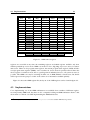
Table 1.1: prefixes
Prefix
K
M
G
Description
kilobinary, 210 = 1024
megabinary, 220 = 1024
gigabinary, 230 = 1024
equivalent IEC prefix
kibi
mibi
gibi
One gigabyte would be written as 1GB, and is the equivalent of 1024MB (megabyte), 1048576KB
(kilobyte) or 1073741824B (byte). Bytes are expected to consist of eight bits (8b).
For all other units the SI symbols will be used, like 10MHz (ten megahertz, a frequency of 10 ∗ 106
Hertz) or 100ns (one hundred nanoseconds, or 100 ∗ 10−9 s= 0.0000001s).
Decimal numbers are written as is, hexadecimals are prefixed with ’0x’ and binary numbers are
prefixed with a single lower case ’b’: 57 = 0x39 = b00111001.
Variable and function names will be typeset in a typewriter font, and register names and bitfields
will be emphasized.
Footnotes1 are sequentially numbered within a chapter, starting at one at the beginning of each
chapter.
1 This
is a footnote.
1
1.3. Prerequisite Knowledge
1.3
2
Prerequisite Knowledge
This master’s thesis builds upon knowledge gained while writing the diploma thesis “Open On-Chip
Debugger - Design and Implementation of an On-Chip Debug Solution for Embedded Target Systems
based on the ARM7 and ARM9 Family” [DR05].
The design of the OpenOCD+trace ETM (Embedded Trace Macrocell) TPA (Trace Protocol Analyzer)
was implemented using VHDL, the VHSIC Hardware Description Language, and the chapter describing
the OpenOCD+trace implementation requires basic knowledge about the language VHDL and synchronous
design.
All software described in this document is written in C and familiarity with the language is assumed.
2
Debugging Techniques
Debugging becomes necessary when software or hardware does not behave the way it was designed to,
and when it is not apparent why it is misbehaving. The deviation from the intended system behaviour
is called a bug, and techniques for observing the circumstances that caused the system to fail is shall be
described in this chapter.
2.1
Static Analysis
One way to avoid bugs at runtime is to eliminate them before code is run for the first time, by making
use of static source code analysis.
Compiler Warnings
C compilers output only a limited number of warnings by default, making it easy to slip ambiguities into
the code that later turn out to be bugs, because the code never described the intended system behaviour.
The following trivial code fragment for example compiles without warnings when using GCC version
4.1.2:
Listing 2.1: test.c
1
2
3
4
5
6
int max (int a , int b) {
if (a > b)
return a;
if (b > a)
return b;
}
However, after enabling additional warnings using the -Wall switch, it becomes apparent what
potential defects this small piece of code contains:
gcc -c test.c -Wall
test.c: In function ’max’:
test.c:6: warning: control reaches end of non-void function
The code is intended to return the greater of the two values, but misses the case when a equals b, in
which the behaviour is undefined.
3
2.2. Debug Output
4
Static Analysis Tools
The Linux kernel is often used as a target for auditing purposes, for example because of its popularity,
complexity, and source code availability. The Sparse (http://www.kernel.org/pub/software/devel/
sparse/) project was specifically created to audit the Linux kernel. It consists of a compiler frontend
that compiles ANSI C and some GCC specific enhancements, and a static analyzer part. Sparse can be
used to convey additional semantic information about types and functions, allowing static verification of
the code.
Coverity (http://www.coverity.com) is the company that offers the commercially available tool
Prevent SQS (software quality system), a software that uses static source code analysis for automated
identification of software defects. Since 2004 Coverity regularly checks the Linux source code for
defects, and later expanded this service to over 150 open source projects. One of the first problems
found by Coverity was the following bug in arch/i386/boot/tools/build.c1 , already fixed since
Linux version 2.6.12:
Listing 2.2: arch/i386/boot/tools/build.c
74
unsigned int i , c , sz , setup_sectors ;
Listing 2.3: arch/i386/boot/tools/build.c
125
126
127
for (i =0 ; (c= read (fd , buf , sizeof( buf ))) >0 ; i += c )
if ( write (1 , buf , c) != c)
die (" Write call failed " );
Variable c was declared as an unsigned int, but the read() system call could return -1. The comparison
intended to catch this error condition wouldn’t identify this, because the negative value would be interpreted as an unsigned value greater zero, causing a huge amount of data to be written on the disk in the
following write call. The read() would presumably continue to fail, resulting in writes to the disk until
it is full and the program exits with the “Write call failed” message.
2.2
Debug Output
One obvious way of gaining insight into the system’s behaviour is the inclusion of debug output, often
referred to as “printf-debugging”. The developer includes printf statements (or the equivalent provided
by the programming language or development environment) throughout the source code wherever information about the current system state is required. This approach has several drawbacks, especially in the
context of embedded systems:
• It requires changes to the source code. Every change to the code could possibly affect the system
behaviour, causing the original problem to disappear or new ones to show up.
• It is a short-sighted debug approach. Debug statements are usually included around the area where
the defect is suspected and removed whenever the problem is believed to be fixed. For the next,
similar problem, debug statements will be included again.
1A
helper program that builds Linux disk images for use on x86 systems.
2.3. Start/Stop Debugging
5
• Debug output could use up one of a limited number of communication channels like UARTs. If
the final product requires the use of all available resources it wont be possible to output any debug
information.
• Output of debug information negatively affects the system’s realtime behaviour. Depending on the
communication channel used to transfer the debug output every access could block the target for
a non-deterministic time. For example when using the ARM7/9 debug communications channel
(see 6) every access would have to block until the previous data was read from the transmit register
by the debugging host.
2.3
Start/Stop Debugging
Start/stop debugging works by halting the target execution at some point to be able to examine the current
system state. Using instruction breakpoints that halt execution once a particular address is reached
and watchpoints that catch data accesses, optionally dependant on an address mask and a certain data
pattern, the system behaviour is observed by gradually moving towards the original point of failure. This
debugging technique requires either hardware support in the form of an in-circuit emulator or on-chip
debug support, or extensive support within the software running on the target, in the form of a debug
monitor or operating system debug facilities.
A disadvantage of this debug technique is the inability to debug problems that depend on realtime
interaction of the microcontroller being debugged with other parts of the system, or problems where
the root cause of the defect is too far away from the part that exhibits the malfunction. When a target
is halted it is usually unable to react upon external events, which can lead to communication timeouts,
missed interrupts, overruns in connected hardware, or other problems unrelated to the defect that is being
debugged. It also requires knowledge about the approximate location of the problem in order to place a
breakpoint or watchpoint that halts the target.
2.4. Trace
2.4
6
Trace
Tracing is an automated way of observing the system behaviour by outputting information about the
current system state at regular intervals. It is similar to debugging via debug output, because it only
allows the system to be observed, eventually up to the level of detail required to determine where
execution deviated from the intended behaviour, but it doesn’t allow execution to be influenced, like
it can be done when using start/stop debugging.
Trace solutions usually allow the instruction flow to be reconstructed up to a certain depth, and
optionally include information about the data accessed by instructions such as loads, stores or coprocessor
transfers. The amount of preprocessing done before the data is captured and the analysis required to
reconstruct the program flow greatly varies.
Often a trigger is used to specify a point at which trace collection is stopped. Using a programmable
counter that starts counting down to zero once the trigger fires, the trace can be configured to capture
data up to the trace point, around the trace point, or starting at the trace point until the maximum trace
depth is reached.
3
Debugging Implementations
3.1
In-Circuit Emulators
An in-circuit emulator (ICE) replaces the target microcontroller with a special debug variant that includes
hardware debugging facilities. The emulator is connected to a host computer which runs the debugger
software. This allows both passive and active debugging, giving a non-intrusive view of the program flow,
and allowing fine control over program execution, CPU state and memory contents. Read Only Memory
(ROM) emulators substitute target non-volatile memory with dual-ported Random Access Memory (RAM)
modules, that can be accessed from a debugger and the target at the same time. Where code has to be
run from ROM this allows a debugger to replace instructions with hooks necessary for debug entry, like
TRAP or Software Interrupt (SWI) instructions. Code testing is improved, as the memory chips don’t
have to be programmed with external tools.
An ICE might support hardware breakpoints, where address comparators constantly monitor the
address bus, and force the system into debug state when an address matches during an instruction fetch.
This allows breakpoints to be set on code contained in ROM without using a ROM emulator. If the
ICE further provides overlay memory, it is possible to load code into the target, replacing instructions
contained in ROM regions. The ICE watches the accessed memory space, and switches to its included
RAM when an access to overlaid memory occurs.
In-circuit emulators have lost significance because modern chip families like the NXP LPC2000,
Atmel AT91SAM7, or ST Microelectronics STR7 come in a wide variety of different devices, making it
difficult to provide drop-in replacements with debug functionality for each of them.
3.2
Debug Monitors
Debug monitors, also called debug stubs, are pieces of software running on the target that communicate
with the debug host using a communications channel and some kind of debug protocol. The debug
protocol allows the host to halt normal execution of the target, to inspect and modify registers and
memory content, and to resume execution again. Breakpoints that halt execution once a certain address
has been reached are usually implemented as well, and if the hardware allows, watchpoints that halt upon
specific memory accesses may be available.
Examples of debug monitors used in embedded systems are the RealMonitor in conjunction with
the EmbeddedICE-RT1 macrocell found on some versions of the ARM7TDMI-S core, the Angel debug
1 The
EmbeddedICE-RT macrocell is an enhanced EmbeddedICE macrocell with support for monitor mode debugging.
7
3.3. On-Chip Debugging
8
monitor, or the gdbserver.
RealMonitor provides a lightweight implementation of a debug monitor that establishes communication between a target and the debug host using the ARM7/9 debug communications channel. It makes
use of the monitor mode debug feature available on EmbeddedICE-RT implementations to implement
breakpoint and watchpoint functionality, and allows IRQ and FIQ exceptions to be serviced during a
debug session, reducing the impact debugging has on realtime behaviour.
The Angel debug monitor is a target resident debug monitor that communicates with a debug host
over a variety of communication channels like the ARM7/9 DCC, a serial link or an TCP/IP connection.
The gdbserver is a standalone application running on supported operating systems that launches the
target application on behalf of the debugger and allows the debugger to control target execution remotely.
Communication can be established over a serial line or using a TCP/IP network connection.
3.3
On-Chip Debugging
Debugging using on-chip debug facilities that allow target execution to be completely halted is the
prevalent debugging technique used with highly integrated targets that embed a microprocessor core,
caches, on-chip memories and a wide variety of peripherals within a single package. The interface used
to control the target hardware is often Joint Test Access Group (JTAG) or some other serial interface like
the background debug mode (BDM) or common on-chip processor (COP) interfaces found on 68k and
Power systems.
While the target is stopped, the debugger has full control over all system resources2 . The debugger
may then examine registers and the target’s memory content, modify system state to analyze the system’s
reaction on those changed circumstances, single step through the code, and eventually resume execution.
Depending on the support provided by the debug facilities, breakpoints may be placed to halt execution
at certain points of interest, and watchpoints could allow specific memory accesses to trigger a target halt,
just like when using debug monitors.
The main advantage start/stop debugging using on-chip debug facilities has over debug monitors
is a lower level of intrusiveness while the target is running. On-chip debugging usually works over
a dedicated communication channel and places no restrictions on the software running on the target.
Debug monitors on the other hand require one of a limited number of communication channels and also
need to be integrated with the target application or operating system. Because the debug monitor requires
code running on the target it also adds to the memory footprint of the target where memory is often a
sparse resource.
Examples for on-chip debug support are the ARM7/9 families with their EmbeddedICE macrocell or
the XScale family with its mini I-Cache that can hold a debug handler.
2 Some implementations provide advanced security features that could potentially limit this access, but during development
it is often possible to gain access to all available resources.
3.4. Software Trace
3.4
9
Software Trace
The simplest kind of trace requires no support from the hardware. It uses an area of memory on the target
system to store trace information generated by the software itself. An alternative approach transfers
the trace information using some kind of communication channel like the ARM7/9 DCC or a serial
connection and stores it on the debug host.
Storing trace data on the target has the obvious drawback of requiring a reserved area of memory.
Also, depending on the nature of the software defect, the trace data itself could get corrupted, rendering
the captured information useless. Transferring trace data to the debug host suffers from similar disadvantages as the debug output approach described before. It requires a communications channel and
potentially affects the system’s realtime performance if the communication causes the target to stall.
3.5
Hardware Trace Support
Several approaches exist that support tracing with dedicated hardware. Hardware trace support usually
has the advantage of being completely unintrusive, but depending on the implementation it might require
physical access to device pins, overflows of the trace information could stall the target, or device pins
used to output trace information might be shared with other target functionality.
Bus Trace
Tracing all accesses at bus level is possible when there is physical access to the bus, usually when using
microprocessors that have no internal peripherals. Another requirement is that all memory accesses
have to be visible on that bus – if intermediate on-chip memories and caches fulfill a request the trace
equipment observing the bus wont see the access.
Logic analyzers with the ability to trace a large number of signals are required to capture the bus
information of a modern 32 or 64 bit processor, because in addition to the data lines the address bus and
control signals need to be traced as well. Filtering out specific accesses is often not possible because
that would require the logic analyzer to decode all trace information on the fly, for example to identify
the location of a memory read. This can be compensated by a large trace depth that allows irrelevant
information to be filtered later during analysis.
An advantage of this trace technique is that it does not require support from the target, that is as long
as the system doesn’t use caches or on-chip memories, bus tracing will work.
Dedicated Trace Port
Targets with higher levels of integration often feature on-chip caches and memories as well as a large
number of on-chip peripherals. Even if those system have an externally available bus there is little insight
3.5. Hardware Trace Support
10
to be gained by tracing only accesses that occur on the external bus. Some targets therefore implement a
dedicated trace port that outputs data similar to a bus trace in a compressed form.
Instruction traces are especially suited for compression, because the program counter increases by a
predetermined amount on each cycle. Branches can also be compressed by outputting only the changes
relative to the last known address, and only indirect branches3 require an address to be output.
Data tracing requires a much higher trace port bandwidth, because often only the addresses can be
compressed, while the data itself shows no recognizable pattern. An ARM9 system for example is able
to read or write one 32 bit word per cycle4 - if the trace port is narrower than that, data needs to be
buffered using FIFOs, or the trace port overflows. Code that processes large amounts of data could still
easily overflow a trace port and its FIFOs, unless the trace implementation provides means to filter the
amount of data that is traced.
Because the trace information is compressed no filtering is possible within the trace capture unit.
Only the target itself has the full address information available and can thus implement filtering, for
example to exclude some known good library code from the trace. When filtering isn’t possible a large
trace depth is required to gain enough information about the system behaviour to be able to analyze the
origin of a bug.
The Embedded Trace Macrocell (ETM) that can be connected to several ARM cores is an example
of a dedicated trace port that outputs compressed trace information over an eight, twelve or twenty bit
wide trace port.
On-Chip Trace
At higher core execution speeds getting the trace information out of the chip package can be be a difficult
problem. The number of device pins that can be used as a trace port is often limited, because higher
pin densities are a driving factor in chip cost and at core frequencies up to and above one gigahertz
maintaining signal integrity is complex task.
Die area on the other hand is getting cheaper with the ever decreasing structure sizes that come with
modern process technologies, which is why some targets provide on-chip memory that directly stores the
compressed trace information, making it available for later analysis via a low-speed interface like JTAG.
Examples for on-chip trace capabilities are the Embedded Trace Buffer (ETB) from ARM that can
be used together with an ARM ETM, or the trace buffer integrated in the XScale core.
3 An indirect branch is branch whose target address can’t be deduced from the program image because it depends on a
register or memory value.
4 Within limits, for example only with zero waitstate memory and when there is no immediate load-use interlock.
4
ARM
This chapter is going to provide an overview on the ARM technologies relevant to the trace debug
techniques described in this master’s thesis. ARM based microcontrollers can be classified by the
architecture implemented, by the core family, and by the actual core used in a design. Table 4.1 has
a list of letters used in ARM core and architecture names and their meaning.
Table 4.1: ARM core features
Letter
T
D
M
I
E
J
4.1
Description
Thumb mode support (compressed 16 bit instruction set)
Debug support
Enhanced Multiplier (multiply with 64 bit)
Embedded-ICE
ARM ’Enhanced’ DSP instruction set
Jazelle Java acceleration technology
Architecture
The targets on which this document focuses implement the ARMv4T and ARMv5TE(J) architecture.
The architecture specifies the programmer’s model and available instruction set. With the exception
of the Jazelle support only available on targets implementing the ARMv5TEJ architecture only small
differences exist as far as the basic execution environment is concerned.
The ARMv5TE architecture adds support for an enhanced DSP instruction set, simplified ARM-Thumb
interworking 1 and a few extra instructions. The Thumb instruction set was assigned a new version
“THUMBv2” [DDI0100E, §7.1.1] which is not to be confused with the “Thumb-2” instruction set
available in ARMv6 and ARMv7.
Programmer’s Model
The execution environment was already described in [DR05, p.13], but some basic information will be
provided here for reference. Detailed information can also be found in [DDI0100E, §2].
The ARM architecture (ARMv4 and ARMv5) defines 31 general purpose registers of which only 16
1 Interworking
means the ability to call ARM functions from Thumb code and vice versa.
11
4.2. Implementations
12
User
FIQ
IRQ
Supervisor
Abort
Undefined
System
R0
R1
R2
R3
R4
R5
R6
R7
R8
R9
R10
R11
R12
R13
R14
PC
R0
R1
R2
R3
R4
R5
R6
R7
R8_fiq
R9_fiq
R10_fiq
R11_fiq
R12_fiq
R13_fiq
R14_fiq
PC
R0
R1
R2
R3
R4
R5
R6
R7
R8
R9
R10
R11
R12
R13_irq
R14_irq
PC
R0
R1
R2
R3
R4
R5
R6
R7
R8
R9
R10
R11
R12
R13_svc
R14_svc
PC
R0
R1
R2
R3
R4
R5
R6
R7
R8
R9
R10
R11
R12
R13_abt
R14_abt
PC
R0
R1
R2
R3
R4
R5
R6
R7
R8
R9
R10
R11
R12
R13_und
R14_und
PC
R0
R1
R2
R3
R4
R5
R6
R7
R8
R9
R10
R11
R12
R13
R14
PC
CPSR
CPSR
SPSR_fiq
CPSR
SPSR_irq
CPSR
SPSR_svc
CPSR
SPSR_abt
CPSR
SPSR_und
CPSR
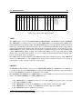
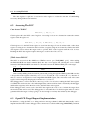
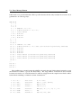
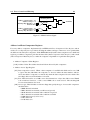
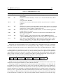
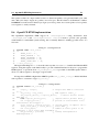
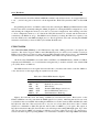
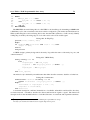
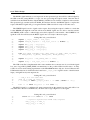
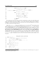
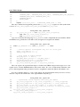
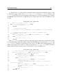
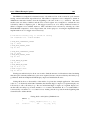
Figure 4.1: ARM banked registers
registers are accessible at any time, the remaining registers are banked registers available only from
within a particular processor mode. ARM core modes are User, FIQ, IRQ, Supervisor, Abort, Undefined
and System. There are six program status registers, the current program status register (CPSR) and five
saved program status registers (SPSR), one for each mode. System mode is special because it shares the
whole register set with user mode, but as a privileged mode unlimited access to all system resources is
possible. The ARM cores may be executing in either one of ARM, Thumb or Jazelle state, but Jazelle
will be ignored for the purposes of this work as there is no information available publicly.
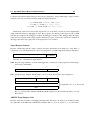
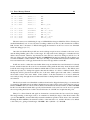
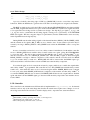
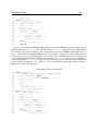
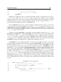
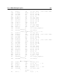
Figure 4.1 shows the ARM register file, the layout of the *PSR registers can be found in figure 4.2.
4.2
Implementations
Cores implementing one of the ARM architectures are available from a number of different vendors,
most importantly ARM itself, but there are also companies holding an ARM architecture license2 that
allows them to roll their own CPU implementing the ARM architecture.
2 See
http://www.arm.com/products/licensing/index.html for the available ARM licensing schemes.
4.2. Implementations
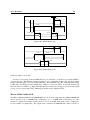
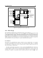
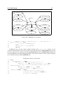
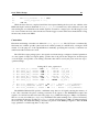
N
Z
C
13
V
Q
J
Reserved
I
F
T
M0 M3 M2 M1 M0
Thumb Bit
T=1: Thumb mode
FIQ interrupt disable flag
F=1: FIQ disabled
IRQ interrupt disable flag
I=1: IRQ disabled
Jazelle Bit
J=1: Jazelle mode
Reserved
Reserved
DSP Overflow/Satuartion flag
Overflow flag
Carry flag
Zero flag
Negative flag
M[4:0]
0b10000 USER
0b10001 FIQ
0b10010 IRQ
0b10011 SVC
0b10111 ABT
0b11011 UND
0b11111 SYS
Figure 4.2: program status register format
ARM7
The ARM7 family consists of the ARM7TDMI, the ARM7TDMI-S, the ARM7EJ-S and the ARM720T.
The ARM720T is a cached processor based on the ARM7TDMI core augmented with a MMU and a
unified 8KB instruction and data cache. The ARM7TDMI employs a 3-stage pipeline with an instruction
fetch stage, a decode stage and an execute stage. It is a Von-Neumann architecture with a single address
space for both instructions and data, and only a single bus between the memory system and the core. The
ARM7TDMI exists both as a hard macrocell tailored for a particular design process and a synthesisable
variant ARM7TDMI-S. When working with synthesizable ARM cores it is important that the JTAG
TCK needs to be synchronized with the core clock. Usually this means that the JTAG frequency must
not exceed one sixth of the core frequency.
The ARM7 family members implement the ARMv4T architecture, with the exception of the ARM7EJ-S
which is an ARMv5TEJ core. The ARM7EJ-S has little practical relevance because no cores based on
this design are readily available at the time of this writing.
ARM9(E)
All ARM9(E) family members are based on a ARM9TDMI, ARM9E-S or ARM9EJ-S core. Only those
cores that are based on the ARM9TDMI core implement the ARMv4T architecture, the newer designs
based on the ARM9E(J)-S implement architecture version 5TEJ.
The ARM920T and ARM922T are ARM9TDMI cores with a MMU and separate instruction and data
caches of 2x16KB (ARM920T) or 2x8KB (ARM922T) size.
• The ARM926EJ-S is a ARM9EJ-S based processor with a MMU and separate caches of variable
sizes between 0MB and 1MB.
• The ARM946E-S is based on the ARM9E-S core with variable cache sizes and a MPU 3 .
• The ARM966E-S is also based on the ARM9E-S but lacks support for a MMU.
• The ARM968E-S features a DMA slave interface.
3 The memory protection unit (MPU). offers protection for memory regions without the need for a paged memory model
that comes with a memory management unit (MMU).
4.2. Implementations
14
The ARM9E(J)-S based processors feature tightly-coupled memory interfaces (TCM) for instructions
and data that allow low latency access at zero or more waitstates. Other memories are typically connected
via the advanced high-performance bus (AHB)and are more loosely coupled to the ARM9E(J)-S core.
Tightly coupled memory is typically used for critical code sequences and critical data that requires
deterministic accesses for which cache memory wouldn’t be suited because of temporal or spatial locality
of the accesses.
The ARM9(E) family uses a 5-stage pipeline with fetch, decode, execute, and writeback stages. The
cores implement a modified Harvard architecture with separate buses for instructions and but still use a
unified address space.
XScale
The XScale family implements the ARMv5TE architecture, and consists mainly of I/O processors (Intel
IOP), network processors (Intel IXP) and application processors (Marvell PXA). In 2006 Intel’s application
processor business was acquired by Marvell, but the I/O processors and networking processors remained
at Intel, making XScale based targets available from two different companies.
This document will only look at the PXA25x, PXA27x and IXP4xx processors for which sufficient
information is available publicly. Other designs, especially the PXA3xx processors could differ significantly
from the implementations described here.
The XScale core features a 7-stage pipeline that splits into a main execution pipeline, a memory
pipeline and a MAC (multiply accumulate) pipeline. Two instruction fetch stages, IF1 and IF2, provide
the following instruction decode stage (ID) with the next instruction that should be executed. The
XScale’s branch prediction logic, implemented in the branch target buffer (BTB), tries to predict the
target of a branch instruction before it reaches the first execution stage (X1) to allow the right instructions
to be fetched into pipeline. The ID stage identifies the instruction opcode and operands, detects undefined
instruction exceptions, and expands instructions that span more than one cycle, for example LDM/STM4 ,
into a sequence of simpler instructions. The register fetch stage (RF) uses the decoded register information
from the ID stage to supply the execution stages, the MAC stages, the data cache and the coprocessor
interface with the required source operands. MAC instructions are then transferred to the MAC pipeline,
all other instructions move on to the X1 stage. In X1 the branch target is calculated, and if it was
mispredicted the pipeline needs to be flushed, because the wrong instructions were prefetched. X1 is
also responsible for ALU (arithmetic-logical-unit) operations and for determining whether a conditional
instruction passes its condition test based on the CPSR flags. During X2 the results that have to be
written to the register file in the write-back stage (XWB) are determined. Once an instruction reached
the XWB stage, it is treated as being completed.
4 LDM:
Load Multiple, STM: Store Multiple.
5
OpenOCD
OpenOCD, the Open On-Chip Debugger, started as a diploma thesis written at the University of Applied
Sciences Augsburg (FH Augsburg) [DR05]. The diploma thesis was completed in July 2005 and the
project got released under the terms of the GNU General Public License (GPL) using BerliOS to host the
project’s code repository: http://developer.berlios.de/projects/openocd/. The current source
code is available from the subversion repository:
svn checkout svn://svn.berlios.de/openocd/trunk
In cases where access using the SVN protocol isn’t possible (e.g. because of company firewalls), the
code can alternatively be acquired using the HTTP protocol:
svn checkout http://svn.berlios.de/svnroot/repos/openocd/trunk
Authenticated access for developers with write privileges is possible using either the SVN+SSH
protocol or via HTTPS:
svn checkout svn+ssh://[email protected]/svnroot/repos/openocd/trunk
svn checkout https://[email protected]/svnroot/repos/openocd/trunk
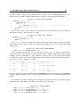
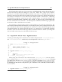
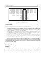
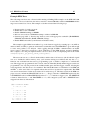
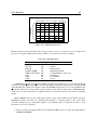
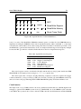
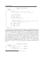
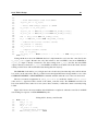
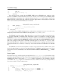
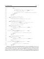
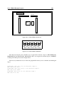
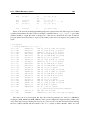
The OpenOCD project website at http://openocd.berlios.de attracts more than 10,000 unique
visitors each month generating almost 55,000 page hits (see figure 5.1). As a convenience for Windows
users a binary package with an installer is available from the yet another GNU toolchain (YAGARTO)
project http://www.yagarto.de. The installer based on SVN revision 141 has been downloaded over
1,100 times during May 2007. Packages are available for the Debian and Ubuntu distributions. There is
no data on the number of source downloads from the Subversion repository.
The OpenOCD project was used as a starting point for implementing the trace functionality that
resulted from this master’s thesis because of the author’s familiarity with the OpenOCD codebase and
because of the wide acceptance the OpenOCD gained during the past two years.
5.1
Current State
At the time of the first public release only ARM7TDMI, ARM720T and ARM920T based targets have
been supported. The only supported JTAG interfaces were the Wiggler and the USBJTAG-1 [DR05,
p.4-5].
15
5.1. Current State
16
Figure 5.1: OpenOCD Website Usage Statistics
The following JTAG interfaces are supported:
• Parallel port wigglers.
Simple PC parallel port interfaces that buffer the parallel port 5V TTL signals for use with lower
voltage JTAG interfaces (typically 3.3V). Parallel port wigglers are available from a large number
of vendors, and support includes cables originally designed to work with programmable logic
devices such as CPLDs and FPGAs.
• Amontec JTAG Accelerator.
A JTAG interface configuration for use with Amontec’s Chameleon parallel port device. The
chameleon consists of a IEEE1284 compatible bus interface and a Xilinx Coolrunner CPLD. See
http://www.amontec.com/jtag_accelerator.shtml for additional information.
• Gateworks GW1602.
A parallel port interface with a proprietary design using a CPLD. See http://gateworks.com/
avila_gw16012.htm for additional information.
• FTDI FT2232 based USB JTAG interfaces. FTDI’s FT2232 features a MPSSE (multiple protocol
synchronous serial interface) that can be used to generate JTAGcompliant signals. FT2232 based
devices are available from a number of vendors and can also be built using schematics available
freely on the internet.
• ASIX PRESTO.
A USB JTAG interface that can also be used to program various other microcontrollers. See
http://www.asix-tools.com/prg_presto.htm for additional information.
• usbprog.
The usbprog is a completely free design using a USBN9604 USB interface chip and an ATMega32
to implement various programmer protocols. See http://www.embedded-projects.net/index.
php?page_id=165 for additional information.
As of SVN revision 194 the OpenOCD supports the following targets:
•
•
•
•
ARM7TDMI(-S)
ARM9TDMI
ARM920T
ARM922T
5.2. Further Development
•
•
•
•
•
•
17
ARM926EJ-S
ARM966E
ARM Cortex-M3
Intel/Marvell PXA25x
Intel/Marvell PXA27x
Intel/Marvell IXP42x
Target debugging is supported with the MMU and caches enabled, and cache coherency is ensured
for targets where this is an issue (e.g. ARM9 based targets with separate instruction and data caches).
When working with ARM920T targets the current cache and TLB content can be examined to identify
potential performance bottlenecks.
Flash programming is supported for the following flashes:
•
•
•
•
•
•
5.2
NXP LPC2000 internal flash
Atmel AT91SAM7 internal flash
STMicroelectronics STR7x and STR9x internal flash
External CFI compatible flashes
Several non-CFI compatible flashes using the AMD/Spansion algorithm
NAND flashes connected to a NXP LPC3180 target
Further Development
So far only ARM based targets have been added to the OpenOCD, but the overall architecture should
support other targets such as MIPS or PowerPC as well. The OpenOCD project constantly adds support
for new flash memories, and support for other memory types like serial dataflash is being considered.
On the fastest interface currently available (FT2232) the USB 1.1 connection limits the OpenOCD’s
performance (download to memory, number of single-step cycles per second). A new design consisting
of a single board computer (SBC) and a FPGA is currently being evaluated, where the OpenOCD would
be running on the linux capable SBC. The OpenOCD’s design with a telnet and GDB remote protocol
interface always intended such a use case, but resource constraints on the SBC might require some
changes.
The community that evolved around the OpenOCD project uses the services (SVN repository, patch
tracker, mailing list) provided by BerliOS (http://www.berlios.de) and a forum hosted at
http://forum.sparkfun.com/viewforum.php?f=18 to organize the development efforts.
6
DCC Software Trace
In cases where no communication channel is left available on the target, for example because all UARTs
are already used for application specific communication, the ARM7/9’s debug unit EmbeddedICE offers
an additional means of communication with a host, the debug communication channel (DCC). From the
ARM core the DCC is accessible via coprocessor 14 using MRC (move to ARM register from coprocessor)
and MCR (move to coprocessor from ARM register) instructions to read and write the coprocessor registers.
The debug host uses JTAG to read and write the DCC control and data registers. Because the DCC is
an unbuffered communication channel the target has to wait for the debugger to read the last transmitted
word before it is able to transmit the next data item. The debugger needs to continuously poll the DCC
to allow the target to continue its operation. This restriction imposes potential problems for time critical
applications, where the additional delays could cause new problems to appear.
This chapter is going to outline how the ARM7/9 DCC can be used for debug output and software
trace functionality.
6.1
DCC Registers
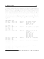
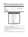
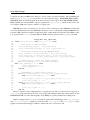
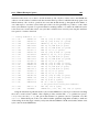
The DCC consists of three registers:
• Control Register: Read-Only.
• Data Read Register: Data sent from debugger to target.
• Data Write Register: Data sent from target to debugger.
The control register contains two bits for handshaking and a version field that indicates the implemented
EmbeddedICE version.
R This bit is set to indicate that the DCC data read register contains a word to be read by the target.
W This bit is set to indicate that the DCC data write register contains a word to be read by the
debugger.
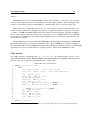
31
28 27
Version
2 1 0
Reserved (RAZ)
Figure 6.1: DCC Control Register
18
W R
6.2. Accessing The DCC
19
The data register is split into a read and a write register to reduce the amount of handshaking
necessary during bidirectional transfers.
6.2
Accessing The DCC
Core Access To DCC
MRC CP14, 0, Rd, C0, C0
CP14 register c0 is the DCC control register. Accessing it via an MRC instruction returns the current
register value in register Rd.
MCR CP14, 0, Rn, C1, C0 MRC CP14, 0, Rd, C1, C0
CP14 register c1 is the DCC data register as seen from the target. It can be written with a value from
register Rd using an MCR instruction and is read into a register using an MRC instruction. Before the DCC
data register can be written the target needs to poll the DCC control register until the W bit is clear.
Reading the DCC data register requires the target to wait for the R bit to be set.
JTAG Access To DCC
The DCC is accessed via the ARM cores JTAGtest access port (TAP)[DR05, p.18]. After writing
the EmbeddedICE scan chain’s number (0x2) into the SCANN register and selecting the INTEST JTAG
instruction the EmbeddedICE scan chain is connected between the TDI and TDO pins of the target:
37 36
W
32
Address
0
Data
After serially shifting in the desired bit pattern and passing through the JTAG Update-DR state the
W bit specifies if the register selected by Address is to be read (W = 0) or written (W = 1). Because of
this, two accesses are required to read a single EmbeddedICE register, but consecutive reads of the same
register can be merged by keeping the W and the Address bits set.
The debugger has to wait for the DCC control reg’s W bit to be set before reading the DCC data register
via JTAG. This read resets the W bit, indicating that the current word has been consumed by the debugger
and that the target may write the next word to the DCC data write register.
If the debugger writes a new word to the DCC data register the R bit is set to inform the target about
the new data that can be read. The debugger has to wait until the R bit cleared again, unless it can be
guaranteed that the target is always going to be fast enough to read any data written by the debugger.
6.3
OpenOCD Target Request Implementation
In addition to using the DCC as a debug and trace message channel, additional functionality can be
implemented in a DCC aware debugger. One common use is called semihosting [ARMSEMI], a method
6.3. OpenOCD Target Request Implementation
20
to enhance target functionality using resources from a debug host. Using semihosting, a target could for
example access a host’s filesystem using standard C library functions:
open(const char *pathname, int flags);
read(int fd, void *buf, size_t count);
write(int fd, const void *buf, size_t count);
Semihosting itself doesn’t necessarily require the use of the DCC, because it can be implemented
using traditional start/stop debugging as well. The program code running on the target would use SWI
calls that are caught by the debugger to request the debugger’s attention. The debugger halts the target,
reads necessary input from the target registers and memory space, executes the system call on behalf of
the target, and writes any replies back to the target before it is resumed.
Target Request Protocol
Because semihosting and the output of debug and trace information both make use of the DCC, a
common protocol was implemented to allow easy integration of semihosting functionality in the future:
8 7
31
Command Specific Data
0
Command
Currently two commands are implemented:
0x00 Trace message. Indicates to the host debugger that a certain part of the program executed using a
24 bit trace point number.
8 7
31
Trace Point
0
Command 0x00
0x01 Debug message. Outputs ASCII strings or 8, 16 or 32 bit data streams on the debug host.
31
8 7
16 15
Type
Length
Data
..
.
Data
0
0x01
Length items of 1, 2, or 4 bytes size
The Type field specifies whether ASCII data (0x0), single bytes (0x1), halfwords (0x2), or words
(0x4) follow.
ARM7/9 Target Request Code
Because of the invasive nature of debugging using the DCC the target code needs to be modified to make
use of the DCC as an additional communication channel. The DCC_READY6.1 and DCC_OUTPUT6.2 macros
6.3. OpenOCD Target Request Implementation
21
use GNU compiler collection (GCC) inline assembly syntax to access the EmbeddedICE coprocessor
(CP14) because standard C language features have no support for such target specific facilities:
Listing 6.1: dcc_debug.c:DCC_READY
1
2
3
4
5
6
#define DCC_READY do {
\
unsigned int dcc_status ;
\
do {
\
asm volatile(" mrc p14 , 0, %0 , c0 , c0 " : "=r" ( dcc_status ) : );
} while ( dcc_status & 0 x2 );
\
} while (0);
\
The DCC_READY macro waits in a busy loop until the W bit is cleared, indicating to the target that DCC
data register is ready to accept a new word of data.
Listing 6.2: dcc_debug.c:DCC_OUTPUT
8
9
10
#define DCC_OUTPUT (x) do {
\
asm volatile(" mcr p14 , 0, %0 , c1 , c0 " : : "r" (( x )));
} while (0);
\
The DCC_OUTPUT macro unconditionally outputs data using the DCC without waiting for the DCC
data register to become empty. It is the responsibility of the calling code to ensure proper handshaking
using the W bit.
Listing 6.3: dcc_debug.c:DCC_TRACEPOINT
void TRACEPOINT (unsigned int num )
If the program’s execution flow is to be observed the TRACEPOINT(num) function can be used to
output a trace point. In the current state the developer needs to manually examine the resulting binary
if linking of trace point numbers to target addresses is desired. The objdump utility from the GNU
toolchain can be used to disassemble an ELF image and the resulting output can be filtered for calls to
the TRACEPOINT macro using the grep utility:
arm-none-eabi-objdump -d main.out |grep
800004fc:
e3a00000
mov
80000500:
eb00012c
bl
-80000814:
e3a00001
mov
80000818:
eb000066
bl
\<TRACEPOINT\> -B1
r0, #0 ; 0x0
800009b8 <TRACEPOINT>
r0, #1 ; 0x1
800009b8 <TRACEPOINT>
The above output shows trace point #0 at address 0x80000500 and trace point #1 at address as 0x80000818.
A simple script could generate a list of trace points and addresses for use with the OpenOCD’s trace
feature.
An alternative approach could integrate the tracepoint mechanism with the code profiling support
available in GCC, gprof and gcov, but that is beyond the scope of this work.
Listing 6.4: dcc_debug.c:DEBUG
void
void
void
void
DEBUGASCII (const char * msg )
DEBUGHEX32 (unsigned int * data , int len )
DEBUGHEX16 (unsigned short * data , int len )
DEBUGHEX8 (unsigned short * data , int len )
6.4. OpenOCD DCC Software Trace Implementation
22
When a developer wants to output debug information from the running program the DEBUG*()
functions can be called to output the data on the debug host. Different functions are provided to print
ASCII strings (DEBUGASCII()) and arbitrary binary data encoded as hex strings in quantities of one, two
or four byte (DEBUGHEX[8|16|32]().
6.4
OpenOCD DCC Software Trace Implementation
The support for software trace is implemented in ./src/target/trace.c, which makes use of the
generic target request code implemented in ./src/target/target_request.c. The per target structure
struct target_s was enhanced to include a pointer to the generic trace information that is stored in a
structure of type struct trace_s.
Listing 6.5: ./src/target/trace.c
25
26
27
28
29
30
31
32
33
34
35
36
37
38
39
40
41
42
43
44
45
46
47
48
49
50
51
typedef struct trace_point_s
{
u32 address ;
u64 hit_counter ;
} trace_point_t ;
typedef struct trace_s
{
int num_trace_points ;
int trace_points_size ;
trace_point_t * trace_points ;
int trace_history_size ;
u32 * trace_history ;
int trace_history_pos ;
int trace_history_overflowed ;
} trace_t ;
typedef enum trace_status
{
TRACE_IDLE = 0x0 ,
TRACE_RUNNING = 0x1 ,
TRACE_TRIGGERED = 0x2 ,
TRACE_COMPLETED = 0x4 ,
TRACE_OVERFLOWED = 0x8 ,
} trace_status_t ;
extern int trace_point (struct target_s * target , int number );
The trace_s structure holds two arrays, one is the list of defined trace points (trace_point_t *trace_points)
and the other contains the history of trace points encountered during the trace run (u32 *trace_history).
Because trace points can be added dynamically from a config file or a command context1 the number of
currently defined trace points and the current size of the array is stored in two members of the trace_s
1 An
OpenOCD command context belongs to an open connection (currently GDB or telnet) and provides access to the
OpenOCD’s command interpreter.
6.5. OpenOCD Target Request Usage
23
structure. A trace point consists of the address at which the trace point is emitted and a hit counter that
is used to keep track about how often a trace point was reached during the current trace run.
The current size of the trace history is kept together with the current position in the history buffer and
a flag indicating a previous overflow. The current position is required when writing to the trace history
buffer and is used together with the overflow flag to identify the oldest item available in the buffer.
The trace_point() function is provided as a callback for the target request subsystem. It gets called
whenever the target reported a trace point and updates the trace information accordingly.
6.5
OpenOCD Target Request Usage
Using the ARM7/9 target request code from 6.4 the target can request services from the OpenOCD
running on a debug host. The only feature currently available from the target_request family of
commands is the display of debug messages:
> help target_request
target_request
target_request commands
debugmsgs enable/disable reception of debug messgages from target
Using target_request debugmsgs [’enable’|’disable’] the user may enable or disable the
output of debug messages to the current command context, which could be either a telnet connection or
a GDB debug session (GDB, Insight, Eclipse).
6.6
OpenOCD Software Trace Usage
As of revision 195 the OpenOCD supports collecting trace information via the ARM7/9’s DCC, but this
could potentially be enhanced to support other target families as well, provided there is a suitable means
of communication. One candidate architecture is XScale with its TX and RX debug registers that provide
communication similar to the DCC.
> help trace
trace
history point -
trace commands
display trace history, [’clear’] history or set [size]
display trace points, [’clear’] list of trace points, or add new
tracepoint at [address]
If the code executing on the target makes use of the TRACEPOINT (see listing 6.3) the OpenOCD
collects data about how often each trace point got called and a history of trace points that executed in the
past.
6.7. ARM7/9 Target Request Constraints
24
The trace history command allows the user to specify the number of previous trace points that
should be kept in a cyclic buffer and is also used to display the trace history.
6.7
ARM7/9 Target Request Constraints
USB JTAG dongles based on the FTDI FT2232 chip are the most popular and versatile debug interfaces
for use with the OpenOCD, but the USB communication has the drawback of introducing a delay of at
least 1ms (USB 1.1 frame length). The handshaking necessary when reading or writing the DCC data
register via JTAG would limit the DCC throughput to 500 ∗ 4byte/s if every control register read and
subsequent data register access would execute within exactly one millisecond.
To improve the DCC transfer performance the OpenOCD DCC receive code pretends that the target
is always going to be fast enough to write the next word into the DCC data register, making handshaking
only a requirement for the first word of a transfer.
When doing continuous transfers the JTAG TAP moves from Update-DR state (where the EmbeddedICE
register is actually read) to the Run-Test/Idle state (1 cycle), from there to Shift-DR (3 cycles) where it
reads the next word (37 cycles) before it moves to Update-DR again (4 cycles), resulting in a minimum
of 45 cycles per access (some JTAG interfaces might introduce additional cycles).
Listing 6.6: DEBUGHEX32
void DEBUGHEX32 (unsigned int * data , int len )
{
DCC_READY ;
80000 aac :
ee103e10
mrc
14 , 0, r3 , cr0 , cr0 , {0}
80000 ab0 :
e3130002
tst
r3 , #2 ; 0 x2
80000 ab4 :
1 afffffc
bne
80000 aac < DEBUGHEX32 >
DCC_OUTPUT (0 x01 | 0 x0400 | (( len & 0 xffff ) << 16));
80000 ab8 :
e1a03801
mov
r3 , r1 , lsl #16
80000 abc :
e3833b01
orr
r3 , r3 , #1024
; 0 x400
80000 ac0 :
e3833001
orr
r3 , r3 , #1
; 0 x1
80000 ac4 :
ee013e10
mcr
14 , 0, r3 , cr1 , cr0 , {0}
while ( len > 0)
80000 ac8 :
e3510000
cmp
80000 acc :
d12fff1e
bxle
{
DCC_READY ;
80000 ad0 :
ee103e10
mrc
80000 ad4 :
e3130002
tst
80000 ad8 :
1 afffffc
bne
DCC_OUTPUT (* data );
80000 adc :
e5903000
ldr
80000 ae0 :
ee013e10
mcr
80000 ae4 :
e2511001
subs
data ++;
r1 , #0
lr
; 0 x0
14 , 0, r3 , cr0 , cr0 , {0}
r3 , #2 ; 0 x2
80000 ad0 < DEBUGHEX32 +0 x24 >
r3 , [ r0 ]
14 , 0, r3 , cr1 , cr0 , {0}
r1 , r1 , #1
; 0 x1
6.7. ARM7/9 Target Request Constraints
80000 ae8 :
80000 aec :
80000 af0 :
e2800004
1 afffff7
e12fff1e
25
add
bne
bx
r0 , r0 , #4
; 0 x4
80000 ad0 < DEBUGHEX32 +0 x24 >
lr
80000 af4 < DEBUGHEX16 >:
len - -;
}
Listing 6.6 shows a disassembly of the DEBUGHEX32 function. After the first handshaked transfer
(the DCC_OUTPUT at 0x80000ab8) the DCC control register is read to see if the W bit is still set. In the
worst case the W bit would be set when reading it first, and cleared on a subsequent read, so the read and
test needs to be done twice, followed by a load of the next word to be transferred and sending that word
to the coprocessor. A maximum of eleven instructions would thus execute between the transfer of two
words. This allows for four cycles per instruction if the JTAG port was clocked at the same speed as the
ARM core, and n ∗ 4 if the core is clocked at 1/n of the core frequency. With the requirement of running
a synthesizable core like the ARM926EJ-S at a JTAG frequency of less than 1/6th of the core frequency
plenty of cycles are available on the target without risking to loose synchronisation between the target
and the debug host.
7
XScale On-Chip Trace
The XScale family of embedded processors features a 256-entry deep on-chip trace buffer to allow the
program execution flow to be reconstructed. After enabling the trace buffer, trace messages are placed
into the trace buffer whenever an indirect branch occurred or when some other event occurred that makes
additional information for trace reconstruction necessary.
The XScale trace buffer can operate in fill-once and in wrap-around mode. Fill-once allows the whole
program execution to be traced, but affects the target’s real time execution, while wrap-around mode
enables the developer to examine the instruction flow that lead to a breakpoint or watchpoint.
If the application is able to tolerate interruptions during target execution, the use of target RAM as
an extended trace buffer allows the debugger to drastically increase the maximum trace depth.
Once the desired trace data has been acquired the collected trace is transferred to the debug host
using the JTAG interface. The debug host then reconstructs the program flow with the help of the target
image. Information about the target memory image is necessary because only target addresses of indirect
branches are output, while direct branches only cause a branch message to be written to the trace buffer.
7.1
XScale Debugging
Debugging XScale based targets is substantially different from debugging ARM7/9 based targets. There
are a number of different XScale implementations available, but for the purpose of this document XScale
debugging will only be concerned with Intel/Marvell PXA25x, PXA27x and IXP4xx targets.
The XScale is an implementation of the ARMv5TE architecture. The targets come with separate
data and instruction caches and an additional mini instruction cache1 . The mini ICache is accessible
only via the JTAGTAPand is used to load a debug handler code. When a debug exception occurs the
target branches to the reset vector 2 and switches into a special DEBUG mode (also called special debug
state (SDS)). The previous CPSR is saved in SPSR_debug and the return address is stored in R14d ebug.
The debugger must have loaded code at the reset vector which then communicates with the debug host
using a set of transfer registers similar to the ARM7/9 DCC.
1 Some
XScale family members include a mini data cache, too.
0xffff0000 in the ARMv4 and ARMv5 architecture. The currently active location
can be implementation defined or it is determined by the V bit in the system control processor’s control register [DDI0100E,
§2.6.9].
2 Exception vectors can reside at 0x0 and
26
7.1. XScale Debugging
27
Mini ICache
XScale models with 32KB come with a 2KB mini ICache that is two-way set associative with a line
length of eight words (32 bytes) and 16 sets.
10 9
31
MVA
5 4
2 1 0
Segment Word -
A 32 bit address selects a word within a line with bits 2-4 and the segment with bits 5-9. Addresses
that are 1024 byte apart go into the same segment, but because of the 2-way set associativity two lines
can occupy the same segment. This is especially important when overloading the reset vectors at 0x00x1f and 0xffff0000-0xffff001f because both locations map to segment 0. No other address with bits 5-9
set to 0 can be loaded into the mini ICache without evicting the overloaded reset vectors from the cache.
The mini ICache is typically loaded while the XScale core is held in reset. That way the debugger
gains control over that target right out of reset. Once the debug handler is loaded the target reset is
deasserted and the core takes the overloaded reset vector and branches to the debug handler.
It is important to note that only code can be fetched from the mini ICache. If load or store operations
access an address that is loaded into the mini ICache the request will still be fulfilled by either the data
cache or main memory. This is a serious restriction because ARM code is typically interspersed with 32
bit constants in so called literal pools that are accessed using PC relative loads 3 . Code running from the
mini ICache must always build immediate operands using data processing instructions.
OpenOCD XScale Debug Handler
The debug handler starts executing at the reset vector which must contain a branch instruction. In ARM
mode a PC relative branch can specify a range of approximately +-32MB. The debug handler must
therefor reside at an address that’s within 32MB of both the high vectors (0xffff0000) and the low vectors
(0x00000000). Furthermore it has to be aligned to a 2KB boundary (least significant eleven bits all zero)
because of the mini ICache organisation. The OpenOCD restricts the base address of the debug handler
to between 0x800-0x1fef800 and 0xfe000800-0xfffff800).
The source for the debug handler can be found in ./src/target/xscale/debug_handler.S. To
simplify building of the OpenOCD without the need for a cross compilation toolchain the SVN repository
also holds a precompiled binary of the debug handler in ./src/target/xscale/debug_handler.bin.
The debug handler initially sets the !GE! bit in the debug control and status register (DCSR), sends
the current core state and waits for commands from the debug host. On reentry to the debug handler the
!GE! bit is examined to see if the debug handler has been running before.
The protocol between the debug host and the target supports several commands:
3 The ARM instruction set uses 32 bit instructions that leave no room for full 32 bit immediate operands.
If a 32 bit constant
is to be loaded this can be achieved using multiple data processing instructions with 12 bit immediate operands (8-bit + 4-bit
rotation [DDI0100E, §5.1.3]) or by loading the constant from memory.
7.2. Trace Message Format
0x00
0x01
0x1n
0x2n
0x30
0x31
0x40
0x40
0x50
0x51
0x52
0x53
0x60
0x61
0x62
28
Read banked register of <mode>.
Set banked register of <mode>.
Read memory from <address> using <count> n-byte accesses.
Write memory from <address> using <count> n-byte accesses.
Resume execution (after restoring system state with 0x01 commands).
Resume execution with trace enabled (after restoring system state with 0x01 commands).
Read coprocessor register <n> (n is an index into a list of supported registers).
Write coprocessor register <n> (n is an index into a list of supported registers).
Clean main cache (write dirty entries back to main memory) using an otherwise unused <cacheclean-area>.
Invalidate complete DCache.
Invalidate complete ICache (not mini ICache).
Wait for outstanding CP15 operations to complete.
Clear sticky-abort bit in the DCSR.
Read trace buffer.
Clean trace buffer.
Inside the debug handler code care has been taken to ensure that the system state isn’t corrupted
before transferring it to the debug host on debug entry or before the target is resumed. A macro
m_send_to_debugger is used when a register needs to be transferred without corrupting any other register,
otherwise the macro m_small_save_reg calls a function that unconditionally sends the content of r0,
saving one instruction (4 byte) per register write or read.
7.2
Trace Message Format
The XScale trace buffer compresses the amount of information that needs to be stored by outputting only
control flow changes, i.e. after a taken branch or an exception. Other instructions increment a counter
that keeps track of the number of executed instructions since the last control flow change. The trace
buffer entries are 8-bit wide:
Table 7.1: XScale trace messages
Name
Exception
Direct branch
Checkpointed direct branch
Indirect branch
Format
b0VVVCCCC
b1000CCCC
b1100CCCC
b1001CCCC
Checkpointed direct branch
Roll-Over
b1100CCCC
b11111111
Description
An exception caused a branch to address bVVV00.
A direct branch (B, BL) occurred.
A direct branch that was additionally checkpointed.
An indirect branch occurred (load to PC or data
processing instruction).
An indirect branch that was additionally checkpointed.
16 instructions have executed since the last control
flow change.
The following listing shows the entry number NNN, the entry EE and whether the entry is a message
byte (00) or part of an address AA (01). In order to determine if an entry belongs to an address the trace
7.2. Trace Message Format
29
buffer needs to be parsed backwards. This is possible because the last entry read (the most recent one) is
guaranteed to be a message byte.
NNN
1
2
3
4
5
6
7
8
9
10
11
12
13
14
15
16
17
18
19
20
21
22
...
247
248
249
EE
00
00
20
00
90
80
ff
ff
ff
00
00
88
e0
97
ff
ff
ff
ff
85
82
82
82
AA
01
01
01
01
00
00
00
00
00
01
01
01
01
00
00
00
00
00
00
00
00
00
Address: 0x00002000
Indirect branch to 0x00002000
Direct branch
Rollover
Rollover
Rollover
address: 0x00088e0
Indirect branch to 0x000088e0
Rollover
Rollover
Rollover
Rollover
Direct Branch (5 instructions
Direct Branch (2 instructions
Direct Branch (2 instructions
(55 instructions previously executed)
previously executed)
previously executed)
previously executed)
82 00
82 00
82 00
The resulting trace output from the OpenOCD is shown in the next listing with an instruction count,
the instruction’s address, opcode and disassembly. The large number of instructions that executed
between trace entries 4 to 55 and between 62 to 201 was stripped from the output because little could be
learned from examining a continuous stream of instructions.
1
2
3
4
...
55
56
57
0x00002000
0x00008800
0x00008804
0x00008808
0xea0019fe
0xe59f0944
0xe3e01000
0xe5801000
B 0x00008800
LDR r0, [r15, #0x944]
MVN r1, #0x0
STR r1, [r0]
0x000088d4
0x000088d8
0x000088dc
0xee120f10
0xe1a00000
0xe24ff004
MRC p15, 0x00, r0, c2, c0, 0x00
NOP
SUB r15, r15, #0x4
7.2. Trace Message Format
58
59
60
61
62
...
201
202
203
204
205
206
30
0x000088e0
0x000088e4
0x000088e8
0x000088ec
0x000088f0
0xe1a00000
0xe1a00000
0xe1a00000
0xe1a00000
0xe3e00000
NOP
NOP
NOP
NOP
MVN r0, #0x0
0x000089f0
0x000089f4
0x000089ec
0x000089f0
0x000089f4
0x000089ec
0xe1540002
0xcafffffc
0xe5932000
0xe1540002
0xcafffffc
0xe5932000
CMP
BGT
LDR
CMP
BGT
LDR
r4, r2
0x000089ec
r2, [r3]
r4, r2
0x000089ec
r2, [r3]
The trace run was recorded during bootup of a PXA250 based target called Karo Triton. Tracing was
enabled immediately out of reset, but trace recording couldn’t trace the very first instruction at address
0x0, because due to the nature of XScale debugging the instruction at the reset vector was simulated
inside the debugger (see 7.1).
Once the trace buffer fills up in fill-once mode a debug exception causes a branch to the reset vector,
and the debug handler gains control of the target. It is important for the debugger to remember the last
address that executed, otherwise any instructions since the last control flow change would be lost. In
this case debug state was entered with the PC at 0x000089f0, but the last instruction flow change was
a branch at 0x89f4 to address 0x89ec. The trace decoding code identified that instruction 0x89ec must
have executed because of the gap between the last trace message and the current PC.
In fill-once mode or when the trace buffer didn’t wrap around the first traced instruction is already
known, and the instruction flow can be reconstructed starting with the first entry from the trace buffer,
but if the trace wrapped around it is unknown which addresses the trace data refers to. The XScale trace
buffer incorporates two checkpoint registers that take the address of a direct or indirect branch. These
checkpoints will be placed about half the size of the trace buffer apart from each other to maximize
the useable content of the trace buffer. If the address of the first instruction of a trace is unknown
trace analysis skips through the trace buffer until either a checkpointed branch or an indirect branch is
encountered.
The first four entries were identified as addressed and can be skipped when trying to reconstruct the
program flow. The fifth entry is an indirect branch message whose target can be seen in the four previous
entries, 0x2000 in this case. We now know that the next instruction executed will be at address 0x2000.
In this case the indirect branch didn’t specify an incremental word count, but even if one was specified
the corresponding instructions couldn’t be traced because no valid PC was acquired at this point.
Entry 6 is a direct branch, and again no instructions executed since the last control flow change.
The image running on the target needs to be examined to identify the target of the direct branch. The
opcode is 0xea0019fe, an unconditionally executed branch that specifies a 24 bit offset to the current PC.
Reading the PC in ARM mode returns the address of the instruction + 8, and the offset has to be shifted
to the left by two, giving a branch target of 0x2000 + 0x8 + (0x19fe « 2) = 0x8800.
7.3. OpenOCD XScale Trace Implementation
31
The following three entries are rollover messages, each indicating that another sixteen instructions
executed since the last control flow change for a total of 48. Entries 10 to 13 are part of an address,
but entry 14 is an indirect branch with an incremental word count of 7, indicating that 55 (48 + 7)
instructions executed since the last direct branch message in entry 6. These were output by the OpenOCD
trace analysis as instructions 2 to 56, followed by the indirect branch as instruction 57. Subtracting
the immediate operand four from the current value of the PC (address + 8) results in a branch to the
instruction following the branch. Usually the source operands of a data processing operation that has the
PC as its destination are not all known, so the XScale placed the indirect branch message together with
the destination address (0x88e0) in the trace buffer.
The remainder of the trace buffer could be analyzed similar to the small part examined here. For
each instruction included in the incremental word count the program counter is simply increased by the
size of an instruction in the current operating mode4 , and in case of a direct branch message the opcode
of the final instruction (the one that caused the message to be output) needs to be examined to determine
the address of the next instruction. The target address of indirect branches is available by looking at the
four trace buffer entries that precede the indirect branch message.
7.3
OpenOCD XScale Trace Implementation
Collecting and analyzing data from the XScale trace buffer is implemented in ./src/target/xscale.c
and ./src/target/xscale.h, with the help of the debug handler code in debug_handler.S.
Listing 7.1: ./src/target/xscale.h
52
53
54
55
56
57
58
59
60
61
62
enum xscale_trace_entry_type
{
XSCALE_TRACE_MESSAGE = 0x0 ,
XSCALE_TRACE_ADDRESS = 0x1 ,
};
typedef struct xscale_trace_entry_s
{
u8 data ;
enum xscale_trace_entry_type type ;
} xscale_trace_entry_t ;
When parsing the collected trace data for the first time in xscale_read_trace() each entry (held in
the data member of the xscale_trace_entry_t type) is assigned an xscale_trace_entry_type, identifying
it as either a trace message (XSCALE_TRACE_MESSAGE) or as part of an address (XSCALE_TRACE_ADDRESS).
The code in xscale_read_trace() also determines the number of valid entries read from the trace buffer
by identifying the first non-zero entry that isn’t part of an address. If no valid entry could be found an
error is returned.
Listing 7.2: ./src/target/xscale.h
64
typedef struct xscale_trace_data_s
4 Four
bytes in ARM mode, two in Thumb mode.
7.3. OpenOCD XScale Trace Implementation
65
66
67
68
69
70
71
72
73
74
75
76
77
78
79
80
81
82
83
84
32
{
xscale_trace_entry_t * entries ;
int depth ;
u32 chkpt0 ;
u32 chkpt1 ;
u32 last_instruction ;
struct xscale_trace_data_s * next ;
} xscale_trace_data_t ;
typedef struct xscale_trace_s
{
trace_status_t capture_status ;
image_t * image ;
xscale_trace_data_t * data ;
data */
int buffer_enabled ;
int buffer_fill ;
read (-1 for wrap-around) */
int pc_ok ;
u32 current_pc ;
armv4_5_state_t core_state ;
Jazelle) */
} xscale_trace_t ;
/* current state of capture run */
/* source for target opcodes */
/* linked list of collected trace
/* whether trace buffer is enabled */
/* maximum number of trace runs to
/* current core state (ARM, Thumb,
Information about the XScale trace data collected is stored in a member trace of type xscale_trace_t
that is part of the XScale specific data (xscale_t). This includes the current state of the trace run, the
image used to read opcodes, a linked list of xscale_trace_data_t items, the mode the trace port currently
operates in (disabled, wrap-around, fill once, fill n-times), and state information for the trace analysis.
A xscale_trace_data_t item contains a number of trace entries, the content of the checkpoint
registers when the trace was collected, the address of the last instruction executed, and a pointer to
the next item in a linked list.
The collected trace data is analyzed in xscale_analyze_trace(). This function iterates through all
items in the xscale_trace_t->data linked list and cycles through the entries collected in each of the
trace runs, skipping items marked as a branch target address (XSCALE_TRACE_ADDRESS). Depending on
the type of the message entry information about the target of the control flow change is stored in next_pc
and if a valid PC was acquired next_pc_ok is set to 1.
If trace analysis acquired the address of the program counter prior to the current control flow change
it is able to print information about the instructions that executed up to this point, including all the
instructions for which overflow message bytes were output. If the control flow change was because of a
IRQ or FIQ exception the current instruction didn’t execute, and the number of instructions that executed
is decreased by one. Every instruction is fetched from the image_t used for trace analysis. When the last
but one instruction is reached and the control flow change was a data abort, the instruction is examined
to see whether it was a load to the program counter. If it was not, the number of instructions executed is
further decremented by one, because only aborts on loads to the PC are included in the incremental word
count, and this was actually the last instruction executed.
7.4. OpenOCD XScale Trace Usage
33
In case the control flow change was a direct branch, the last instruction that executed is examined to
read the branch target address from the opcode and the program counter is updated accordingly. It is not
necessary to identify the branch targets of instructions that were included in the incremental word count
because if one of those was a branch it didn’t pass its condition test, otherwise it would caused a trace
message to be output.
Every instruction is then output to the current command context (a telnet or GDB connection), and if
the trace buffer entry specified a valid new PC it is saved as the trace context’s current PC.
7.4
OpenOCD XScale Trace Usage
xscale
trace_buffer dump_trace_buffer analyze_trace trace_image -
xscale specific commands
<enable|disable> [’fill’ [n]|’wrap’]
dump content of trace buffer
analyze content of trace buffer
load image from <file> [base address]
The OpenOCD allows the trace buffer to be enabled either in wrap-around or in fill-once mode.
If fill-once mode is selected, an optional number of fills can be selected, in which case the target is
immediately resumed after a debug entry if the reason for debug entry was a trace buffer full event and
there are additional fills to be collected. This allows larger trace runs to be captured with reduced effects
for realtime execution.
For analysis of the trace buffer an image is needed which can be specified by the xscale trace_image
command. This image can be one of the supported image file formats or a pseudo image which reads the
target’s memory to analyze the executed instructions. The collected trace data may also be dumped to
a file for analysis with external tools via the dump_trace command. Trace analysis is started using the
analyze_trace command.
8
ETM - Embedded Trace Macrocell
The embedded trace macrocell (ETM)allows real-time tracing of instructions and data as an ARM core
executes. It connects directly to the ARM core inside an ARM based ASIC and outputs trace data
on a trace port. Trace data is generated at the full processor clock, i.e. every individual core cycle
may be observed, but the trace port may be clocked at a lower frequency using half-rate clocking and
demultiplexing.
This master’s thesis focuses on tracing for ARM7 and ARM9 based targets and will be limited to the
ETM variants currently implemented for these cores. Three major versions of the ETM architecture exist,
but only ETMv1 is implemented by the ETM7 and ETM9 found on ARM7 and ARM9 based targets.
There are also several minor versions ETMv1.0 to ETMv1.3 but all the targets used with the prototype
implementation that results from this master’s thesis implement ETMv1.2 or higher so this document
will ignore the differences that come with older variants of the ETMv1 architecture. The differences
between ETMv1.2 and ETMv1.3 are:
• Support for FIFOFULL. The use of FIFOFULL would allow the core to be stalled before the
ETM’s internal FIFO overflows, but FIFOFULL requires support from both the ETM and the
system. FIFOFULL currently isn’t used by the software written for this master’s thesis so the
difference between ETMv1 and ETMv2 doesn’t matter here.
• Support for tracing Java code. This is required for cores with Jazelle code that have native support
for Java bytecode. Because there is no public information available on the Jazelle technology there
is no support for Java available, so this difference doesn’t matter either.
Older versions of the ETM architecture have more important differences that affect how tracing is
controlled and filtered, but these shall be ignored in this document.
The targets with included ETM functionality examined for the purpose of this thesis are the NXP
LPC2294, an ARM7TDMI-S based microcontroller on an Olimex LPC-H2294 headerboard, the ST
Microelectronics STR912 o a Hitex STR912 Evalboard and the NXP LPC3180, an ARM926EJ-S based
microcontroller on a Phytec phyCORE-LPC3180 single board computer. See table 8.1 for the ETMs
used in these targets.
34
8.1. JTAG Access
35
Table 8.1: ETM implementations
Target
NXP LPC2294
STM STR912
NXP LPC3180
TDI
37 36
nR
Address
W
ETM
ETM7 Rev1 implementing ETMv1.2
ETM9 r2p2 implementing ETMv1.3
ETM9 r2p2 implementing ETMv1.3
31
0
D31
D0
TDO
Figure 8.1: ETM Scan Chain
8.1
JTAG Access
The ETM registers can be programmed via the ARM core’s TAP controller using scan chain 6 in way
similar to the EmbeddedICE registers that are accessible via scan chain 2 [DR05, §3.3]. The debugger
loads the SCAN_N instruction into the JTAG instruction register, scans the number of the ETM scan
chain into the JTAG data register, and selects the INTEST JTAG instruction to read and write the ETM
registers.
Figure 8.1 shows the layout of the ETM scan chain. Like the EmbeddedICE scan chain it consists of
a 32 bit data field, a 5 bit address field, and a read/write bit.
8.2
Trace Port
The trace port of ETMs implementing the ETMv1 architecture consists of the pins listed in table 8.2:
Table 8.2: ETMv1 trace port
Signal
TRACECLK
PIPESTAT[2:0]
TRACEPKT[n:0]
TRACESYNC
Description
The trace clock, running at the full processor speed, but optionally divided by 2 or 4.
The current pipeline status, i.e. what the core actually did in this trace cycle.
An output of 4, 8 or 16 bits from the ETM’s FIFO containing trace information.
A synchronization signal used to match the TRACEPKT output to PIPESTAT cycles.
Because of the high frequency at which trace data is output a special connector type called “MICTOR”
(matched impedance connector) is specified for use with ETM target connections. The use of Mictor
connectors and cables allows for transmission at 200MHz and higher.
The separation of the PIPESTAT signals that closely follow the processor pipeline and the TRACEPKT
signals allow a FIFO to be used when outputting the trace information. The TRACESYNC signal is used
to synchronize between PIPESTAT and TRACEPKT.
8.3. Event Resources
36
Multiplexed mode Demultiplexed mode
Normal mode
PIPESTAT[0]_A
PIPESTAT[1]_A
PIPESTAT[2]_A
TRACESYNC_A
TRACEPKT[0]_A
TRACEPKT[1]_A
TRACEPKT[2]_A
TRACEPKT[3]_A
not connected
not connected
not connected
not connected
PIPESTAT[0]
PIPESTAT[1]
PIPESTAT[2]
TRACESYNC
TRACEPKT[0]
TRACEPKT[1]
TRACEPKT[2]
TRACEPKT[3]
TRACEPKT[4]
TRACEPKT[5]
TRACEPKT[6]
TRACEPKT[7]
VSupply
VTRef
EXTRIG
DBGACK
TRACECLK
not connected
not connected
PIPESTAT[0], TRACESYNC
PIPESTAT[1], TRACEPKT[1]
PIPESTAT[2], TRACEPKT[2]
TRACEPKT[0], TRACEPKT[3]
TRACEPKT[4], TRACEPKT[5]
TRACEPKT[6], TRACEPKT[7]
TRACEPKT[8], TRACEPKT[9]
TRACEPKT[10], TRACEPKT[11]
TRACEPKT[12], TRACEPKT[13]
TRACEPKT[14], TRACEPKT[15]
not connected
not connected
38
36
34
32
30
28
26
24
22
20
18
16
14
12
10
8
6
4
2
37
35
33
31
29
27
25
23
21
19
17
15
13
11
9
7
5
3
1
Normal mode
Demultiplexed mode Multiplexed mode
TRACEPKT[8]
TRACEPKT[9]
TRACEPKT[10]
TRACEPKT[11]
TRACEPKT[12]
TRACEPKT[13]
TRACEPKT[14]
TRACEPKT[15]
nTRST
TDI
TMS
TCK
RTCK
TDO
nSRST
DBGRQ
GND
not connected
not connected
PIPESTAT[0]_B
PIPESTAT[1]_B
PIPESTAT[2]_B
TRACESYNC_B
TRACEPKT[0]_B
TRACEPKT[1]_B
TRACEPKT[2]_B
TRACEPKT[3]_B
not connected
not connected
not connected
not connected
not connected
not connected
not connected
not connected
Figure 8.2: ETM Port Pinout
Trace Port Modes
The trace port may operate in normal, multiplexed or in demultiplexed mode:
• In normal mode all signals from the trace port are directly routed to device pins. The TRACECLK
runs at either the full core clock or at half the core clock, if half-rate clocking is enabled. Halfrate clocking is used to reduce the signal transition frequency and requires the trace port analyzer
(TPA)to capture data on both edges of the TRACECLK.
• Multiplexed mode is used when only few pins can be dedicated to outputting the trace information.
The TRACECLK runs at the full core clock, but the pins output multiplexed data on both edges of
the clock, i.e. a single pin outputs the information of two trace signals.
• Demultiplexed mode is used to reduce the signal transitioning rate by outputting trace data over
twice as many pins at half the core’s frequency. If half-rate clocking is enabled the TRACECLK
is further divided by two and runs at fcore /4.
Figure 8.2 shows the pinout used with a single 38-pin ETM connector. If a demultiplexed ETM port
would be used with a wider trace port (8 or 16 bit) a second ETM connector would be required, but this
is beyond the scope of this document. If a trace port doesn’t use the full 16 bit unconnected signals must
be connected to ground (GND).
8.3
Event Resources
Resources
The ETM provides a wide variety of resources that can be used to control and filter tracing. These
resources are based on memory accesses or are derived from memory accesses. A memory access can be
either a data or an instruction fetch and may depend on an address, a data pattern, or combination of both.
8.3. Event Resources
37
State 1
State 2
State 3
Figure 8.3: ETM Sequencer
6
4 3
Resource
Type
0
Resource
Index
Figure 8.4: ETM Resource
The following list shows the resources available in the ETMv1 architecture:
• Memory access resources
– Single address comparators that match on instruction or data accesses, optionally combined
with a data comparator to match only when a certain word is read from an address.
– Address range comparators are like single address comparators but match on a whole address
range instead of a single address. An addres range comparator matches when an address is
>= address A and < address B.
– EmbeddedICE watchpoint comparators can be used if the RANGEOUT feature supported.
They operate similar to single address comparators.
– Memory map decoders divide the ASIC specific memory map for example to identify onchip RAM, ROM and registers. Using the memory map decoder requires further information
from the chip vendor.
• Derived resources Derived resources allow more complex terms to be formulated by combining
memory access resources with additional logic:
– 16 bit counters that count down at the full system clock with a counter enable event based on
any of the other event resources.
– The sequencer is a three state statemachine as shown in figure 8.3. This allows multi-stage
triggers to be set up, for example to trigger only inside function X if function Y was called
before. The state machine advances to another state based on events from other resources.
• External resources
– Hardwired “true” is a resource that’s always true.
– External inputs are ASIC specific inputs that can be true or false.
ETM resources as shown in figure 8.4 are defined by the type of resoure, encoded in bits six to four,
and a four bit index in bits three to zero. The resource type is one of the types listed in table 8.3, and the
index selects a particular instance of the selected resource, like an address comparator pair or one of the
counters. Table 8.3 shows how the Resource Type encoding maps to the ETM resources described above.
8.3. Event Resources
38
Only indexes from the defined range may be used when selecting a resource as an input to an event.
Table 8.3: ETM resource types
Encoding
000
001
010
011
100
101
110
111
Description
Single address comparator 1-16, indexed as 0-15
Address range comparator 1-8, indexed as 0-7
EmbeddedICE comparator 1-2, indexed as 0-1
Memory map decode 1-16, indexed as 0-15
Counter 1-4 at zero, indexed as 0-3
Sequencer in states 1-3, indexed as 0-2
External inputs 1-4, indexed as 0-3, or hardwire ’true’, index 15
Reserved
The resources available in a particular ETM implementation can be read from the ETM configuration
code register, and should be used in conjunction with the System configuration register to determine the
capabilities offered by the combination of ETM and ASIC:
• ETM configuration code register
[23]
[22:20]
[19:17]
[16]
[15:12]
[11:8]
[7:4]
[3:0]
FIFOFULL present
Number of ext. outputs
Number of ext. inputs
Sequencer present
Number of counters
Number of memory map decoders
Pairs of data comparators
Pairs of address comparators
• System configuration register
[8]
[7]
[6]
[5]
[4]
[3]
[2:0]
FIFOFULL supported
Demultiplexed trace data format supported
Multiplexed trace data format supported
Normal trace data format supported
Full-rate clocking supported
Half-rate clocking supported
Maximum port size. See table 8.5 for the supported encoding.
The targets chosen for the prototype implementation of ETM trace analysis offer a very different
amount of resources, one implementing the large standard and two implementing only the small standard
[IHI0014N, §2.12.2].
Events
An ETM event is the boolean combination of up to two resources, allowing complex conditions to be set
up. The layout for all ETM event registers is the same and is shown in figure 8.5.
8.3. Event Resources
39
Table 8.4: ETM configurations
Feature
Pairs of address decoders
Data value comparators
Memory map decoders
Counters
Sequencer present
External inputs
External outputs
FIFOFULL present
FIFODEPTH
Max. port size
Port mode
Trace data format
LPC2294
1
0
4
1
No
2
0
Yes
10
4
Half-Rate
Normal
STR912
1
0
4
1
No
2
0
Yes
9
4
Full-Rate
Normal
LPC3180
8
8
16
4
Yes
4 (not wired)
4 (not wired)
Yes
45
16 (wired to ETB)
n/a
Normal
• ETM Event registers
[16:14 ] The boolean function that defines how the two resources are combined to generate the event
output.
[13:7 ] Resource B, the second operand to the boolean function.
[6:0 ] Resource A, the first operand to the boolean function.
16
14 13
7 6
Boolean Res.
Function Type
Res.
Index
Resource B
0
Res.
Type
Res.
Index
Resource A
Figure 8.5: ETM Event
The following encodings for boolean functions exist:
000
001
010
011
100
101
110
111
A (Event is true when resource A is true)
Not(A) (Event is true when resource A is false)
A And B (Even is true when both resources A and B are true)
Not(A) And B (Event is true when A is false and B is true)
Not(A) And Not(B) (Event is true when neither A nor B is true)
A Or B (Event is true when A or B is true)
Not(A) Or B (Event is true when A is false or B is true)
Not(A) Or Not(B) (Event is true when A or B is false)
8.4. Trace Control And Filtering
40
Enabling Event
EnOnOff
Trace Start/Stop
Resource
TraceEnable
Exclude/Include
Address Comparator 1−16
Address Range 1−8
Memory Map Decoder
Figure 8.6: ETM TraceEnable Signal
8.4
Trace Control And Filtering
Various options are provided to configure which aspects of the program execution should be traced.
The ETM resources can be used to control starting and stopping of the trace and to trigger around a
certain point of interest. Trace start/stop allows the tracing to be limited to an area of interest, for example
to addresses in which a user’s application is located, preventing areas that are part of the operating system
or some library from being traced.
Triggering is important when the trace data can’t be examined on the fly and all trace information is
written into a buffer for later examination. A trigger counter starts counting down to zero once the trigger
condition is met. Once the counter reaches zero the trace capture is disabled. If the trigger counter is
initialized with a low value compared to the buffer depth the useable trace contains data from before the
trigger point. A value around half of the buffer’s depth is used to trace around the point of interest, while
a large value allows what happened after the trigger to be traced. There will only be one trigger output
during a trace run, and the ETM needs to be programmed again to reenable generation of the trigger
signal.
The TraceEnable (see figure 8.6) signal is used to decide when core execution should be traced. The
ETM continuously outputs data on the trace port, but formats the output so that a trace port analyzer
(TPA) only captures data when TraceEnable is high and there is data to be traced.
The ViewData (see figure 8.7) signal indicates whether data for a data load or store instruction is
to be traced. Especially the amount of data tracing needs to be carefully limited via ViewData to avoid
overflowing a narrow trace port. An ARM9 core is capable of loading one word per cycle from zero
waitstate memory (usually cache or DTCM 1 ), but the trace port is only 16 bit wide at most. Tracing the
address of a data access causes five packets of eight bits size to be output, and if the data content is to be
traced, too, another four packets will be required to trace a 32 bit access.
1 Data
Tightly Coupled Memory, see 4.2
8.4. Trace Control And Filtering
41
Enabling Event
Address Comparator 1−16
Address Range 1−8
Memory Map Decode 1−16
Exclude Only
Address Comparator 1−16
Address Range 1−8
Memory Map Decode 1−16
Include
ViewData
Exclude
Figure 8.7: ETM ViewData Signal
Address And Data Comparator Registers
For every address comparator implemented by an ETM an Address Comparator Value Register and an
Address Access Type Register is provided, allowing the address and type of the access to be specified that
should be monitored by the comparator. If the ETM additionaly features data comparators two additional
registers per address comparator pair take the data value (Data Comparator Value Register) and a mask
(Data Comparator Mask Register) to make the comparator dependant on a particular data pattern.
• Address Comparator Value Register
[31:0] Address Value. The address that should be monitored by this comparator.
• Address Access Type Register
[6:5] Data comparison control. When a data comparator is available this field can be set to b00
to ignore the data, b01 limits the comparator to accesses where the data matches, and b11
causes the address comparator to match only when the data comparator doesn’t match. The
encoding b10 is reserved and must not be used.
[4:3] Size. This field can be set to b00 to trace Java instructions or byte data, b01 to trace Thumb
code or half-word accesses, or b11 to trace ARM code or word accesses. The encoding b10
is reserved and must not be used.
[2:0] Access type. This field has several encodings that specify the type of access this comparator
should monitor:
∗ b000: Instruction fetched
∗ b001: Instruction executed (condition test ignored)
∗ b010: Instruction executed with condition test passed
∗ b011: Instruction executed with condition test failed
∗ b100: Data access (load or store)
∗ b101: Data load
∗ b110: Data store
8.4. Trace Control And Filtering
42
• Data Comparator Value Register
[31:0] Data Value. The data value that should be monitored by this comparator.
• Data Comparator Mask Register
[31:0] Data Mask. Bits programmed as one are ignored when comparing the data.
The data value and mask must be programmed to compare only valid bytes in a transfer depending
on the access size, address and endianness of the memory system. For example to watch the byte at
address 0x1001 for value 0xVV on a little-endian system the value has to be set to 0x0000VV00 with a
mask of 0xffff00ff.
TraceEnable Registers
The TraceEnable signal is controlled by the following registers:
• Trace Start/Stop Resource Control Register
[31:16] Select single address comparator 1-16 as stop address
[15:0] Select single address comparator 1-16 as start address
• TraceEnable Control 2 Register
[15:0] Select single address comparator 1-16 for include/exclude control
• TraceEnable Event Register
[16:0] TraceEnable Event
• TraceEnable Control Register
[25]
[24]
[23:8]
[7:0]
EnOnOff (1: Tracing controlled by on-/off-address)
Exclude/notInclude (0: Include, 1: Exclude)
Select memory map decode 1-16 for include/exclude control
Select address range comparators 1-8 for include/exclude control
The EnOnOff control bit causes the start/stop resource to be don’t care if 0 (EnOnOff is a negated
input to the OR element). The Exclude/notInclude bit is an input to an XOR element causing the output
to be the negation of the preceding OR element if high.
ViewData Registers
The ViewData signal is controlled by the following registers:
• ViewData Event Register
[16:0] ViewData Event
8.4. Trace Control And Filtering
43
• ViewData Control 1 Register
[31:16] Select single address comparator 1-16 for exclude control
[15:0] Select single address comparator 1-16 for include control
• View Data Control 2 Register
[31:16] Select memory map decode 1-16 for exclude control
[15:0] Select memory map decode 1-16 for include control
• View Data Control 3 Register
[16] Exclude only (0: Mixed mode, 1: Exclude only)
[15:8] Select address range comparators 1-8 for exclude control
[7:0] Select address range comparators 1-8 for include control
The Exclude only bit set to 1 causes the Include signal to be unconditionally high, resulting in
ViewData matching all accesses that are not specifically excluded. If Exclude only is 0 the Include signal
is controlled by matches of the address comparators and memory map decodes, resulting in matches only
when an access is included but not excluded.
ETM Trace Control Registers
• ETM Control Register
[17:16] Port mode. Whether the port operates in normal mode (b00), multiplexed mode (b01) or in
demultiplexed mode (b11).
[15:14] Context ID Size. Number of bits from the context ID that should be traced. None (b00), bits
[7:0] (b01), bits [15:0] (b10) or bits [31:0] (b11).
[13] Half-rate clocking. Whether the TRACECLK should be divided by two, resulting in a
frequency of fcore /2 (in normal port mode) or fcore /4 (in demultiplexed port mode).
[12] Cycle accurate tracing. Causes the trace data to be formatted so that every cycle with
TraceEnable high will be traced, even when there is nothing to be traced (i.e. waitstates
or internal cycles and no trace packet).
[11] ETM port selection. Needs to be set to 1 to enable use of the ETM pins as the trace port
mode. If 0 these bits can be used as GPIO.
[10] ETM programming. This bit has to be set to 1 before ETM registers can be programmed.
[9] Debug request control. Allows the ETM trigger event to be used as a debug request. If set to
1 and a trigger occurs the DBGRQ signal is asserted until the core acknowledges debug via
the DBGACK signal.
[8] Branch output. Setting this bit causes all branches to output an address. This allows the
execution flow to be reconstructed without an available image.
[7] Stall processor. The FIFOFULL signal allows the core to be stalled when the FIFO is about
to overflow (using a programmable high-water-mark) if this bit is programmed to 1.
[6:4] Port size. Specifies the width of the TRACEPKT output. See table 8.5 for valid port size
encodings.
[3:2] Data access. Causes nothing (b00), data portion (b01), address portion (b10) or both parts
(b11) of a data access to be traced.
8.5. ETM Trace Format
44
[1] Monitor CPRT. If set to 1 coprocessor register transfers will be traced.
[0] ETM power down. Out of reset the ETM is powered down and only the ETM control
register may be accessed to program this bit to 1. If set to 1 all parts of the ETM can be
accessed.
• Trigger Event Register
[16:0] The event used to trigger the trace capture. See figure 8.5 for the encoding.
• ETM Status Register
[2] The current status of the trace start/stop resource. If high, a start address has been traced but
no stop trace was encountered yet.
[1] Allows the value of the ETM control register’s, ETM programming bit to be read back. This
bit needs to be polled until it goes high before ETM registers may be programmed.
[0] FIFO overflow. This bit is high if an overflow occurred that hasn’t been traced already.
Table 8.5: ETM port size encoding
Encoding
b000
b001
b010
8.5
Description
4 bit port
8 bit port
16 bit port
ETM Trace Format
The ETM outputs the current PIPESTAT[2:0] for each cycle executing, see table 8.6 for the encoding.
Trace packets are always 8 bits wide, no matter what the current ETM port size is set to. In case of a 16
bit trace port up to two trace packets can be output in one cycle, and if a 4 bit port is used a trace packet
is output in two consecutive cycles.
A trace packet can be output on each cycle except in TR or TD cycles. The packets that belong to one
PIPESTAT (e.g. a BE PIPESTAT with its associated branch address) will be output as a continuous block
with no other packets in between. Gaps in the output only exist when the PIPESTAT would be WT which
is turned into a TD and FIFO draining is deferred. Packets for a particular instruction wont start together
with or before the PIPESTAT for the previous instruction was output, but may follow immediately after
the preceding instruction, before the PIPESTAT to which the packets belong is output.
Special rules apply to 16 bit wide ports where it is possible to output two trace packets in a single
cycle. The first packet of a branch will always be output on TRACEPKT[7:0]. A single packet will only
be output if the PIPESTAT is not WT - during WT cycles there will usually be two packets, otherwise
draining is stopped until there is another functional PIPESTAT or until there are at least two trace packets
to be output. There are exceptions that cause a single packet to be output even though the current
PIPESTAT is WT. This is the case when the FIFO is being drained after an overflow, if the ARM core is
in debug state, or when the FIFO is being drained after tracing was disabled.
8.5. ETM Trace Format
45
Table 8.6: ETM PIPESTAT encoding
Encoding
b000
Mnemonic
IE
b001
ID
b010
IN
b011
WT
b100
BE
b101
BD
b110
TR
b111
TD
Description
Instruction executed. An instruction executed but generated no associated
trace packet.
Instruction executed with data. A load or store executed and the data, address
or both
were placed into the FIFO.
Instruction not executed. An instruction didn’t execute because its condition
code test
failed.
Waitstate. No instruction executed and the pipeline didn’t advance, for example
because the memory system delayed an access or because the core executed an
internal cycle. A trace packet is output in this cycle.
Branch executed. An indirect branch executed, or a direct branch required the
branch address to be output.
Branch executed with data. A data access had ViewData enabled and loaded
the program counter.
Trigger. A trigger occurred and replaced the original PIPESTAT which is
output in TRACEPKT[2:0] instead. No other trace packet is output in this cycle.
Trace disabled. This PIPESTAT is output when TraceEnable is low or when
there is no trace packet to be output. In cycle accurate tracing TD is output
with TRACEPKT[0] high to indicate that TraceEnable was high.
Exceptions are traced as branches to the corresponding vector. Depending on the type of exception
this means that the current instruction was interrupted (Reset, IRQ, or FIQ) or executed and was then
turned into a branch to the exception vector (Prefetch Abort, Data Abort, Undefined Instruction or SWI).
Branch addresses and addresses of data accesses are output as up to five packets with the eighth bit
indicating that more packets follow (8th bit set). If less than five packets are output those bits that were
output replace the bits from the previous address. This means that after tracing started a full branch
address output is needed to acquire a complete 32 bit address. Earlier branches that output only part of
the address can’t be traced because the branch target address will be unknown.
32
J
Reason
[31:28] 1
16
24
[27:21]
1
[20:14]
8
1
[13:7]
0
1
[6:0]
The Reason given in a full branch address output provides further information about the branch. The
valid reason codes are given in table 8.7, other codes are reserved.
Following a branch two instructions that have already been fetched will have to be discarded, and
the pipeline needs to be refilled. Figure 8.8 shows how a branch was fetched, followed by fetching two
instructions (I+1 and I+2) from the current instruction stream. By the time the branch reached the execute
stage the destination of the branch is calculated and instruction I+2 is fetched, because at that point is
already too late to prevent the fetch. The branch instruction remains in the execute stage, the fetch and
decode stages are flushed, and a new instruction is fetched from the new location (N). In the next cycle
another instruction is fetched (N+1), the previously fetched instruction advances into the decode stage,
8.5. ETM Trace Format
46
Table 8.7: ETM Branch Reason Code
Encoding
b000
b001
b010
b011
b100
Description
Normal PC change
Tracing enabled
Trace restarted after FIFO overflow
Exit from debug state
Periodic synchronization point
F
D
E
M
W
B
I−1
...
...
...
I+1
B
I−1
...
...
B
I−1
...
I+2 I+1
B
N
N+1
N
N+2 N+1
I−1
B
N
B
Figure 8.8: ARM Pipeline during a branch
while the branch still occupies the execute stage. The branch is then free to move into the memory stage
(nothing happens there for a branch) and instruction N gets executed. While figure 8.8 refers to a 5-stage
ARM9 pipeline the same mechanisms apply to a 3-stage ARM7 pipeline where the execute stage is the
third stage, too.
These two prefetch cycles during which the branch instruction occupies the execute pipeline stage
are reused by the ETM to output an address packet offset (APO) that is used to synchronize between the
PIPESTAT and TRACEPKT signals. During the first APO cycle the lower two bits of the address packet
offset are output on PIPESTAT[1:0], the second APO cycle outputs the higher two bits. PIPESTAT[2]
isn’t used during an APO to be able to identify a BE/BD PIPESTAT that is immediately followed by
another BE/BD PIPESTAT, discarding the previous branch. A TR PIPESTAT might also occur at any
time and can be identified similarly. The APO specifies the number of branch addresses (packets with
TRACESYNC high) that have to be skipped to get to the address that belongs to the current branch (the
one that caused the APO).
8.5. ETM Trace Format
47
Example ETM Trace
The following trace data was collected while running a blinking LED example on the NXP LPC3180
board. The code was loaded into the microcontroller’s internal SRAM at address 0x08000000 and the
target was resumed out of reset. The example code then executed the following steps:
•
•
•
•
•
Prepare stacks for each core mode
Enable PLL to run at 208MHz
Enable SDRAM running at 104MHz
Relocate text section to SDRAM and jump to address in SDRAM
Generate page table to directly map memory areas with appropriate cacheable (IRAM/IROM,
SDRAM) and bufferable (IRAM, SDRAM) settings.
• Enable MMU and caches (both instruction and data cache)
The example toggles LEDs in an endless loop, waits between toggles by counting up to one million,
and uses inline assembly to generate an instruction stream that causes the ETM FIFO to grow full enough
to cause trace packets to be delayed. After toggling through all LEDs a hundred times an invalid
access causes a data abort exception to allow verification of the ETM analysis exception handling.
The complete code and precompiled binaries can be found on the accompanying CD in the folder
examples/lpc3180_gcc_blinky_sdram_cached_abort/.
The trace run was set to collect both the address and the data of all accesses (the ViewEnable signal
was set to include the whole memory area), cycle accurate tracing was enabled, and only the wait()
function was excluded from the trace by programming a pair of address comparators to exclude this
area. The trigger was programmed to the location of the abort handler (0x10) and the trigger counter was
programmed to use only ten percent of the available buffer space after the trigger occurred, allowing the
events that lead to the data abort to be examined. The LPC3180 features a combination of an ETM and
an ETB 2 to allow trace data to be captured without the need for a separate trace capture unit. The ETM
was used in normal trace format mode with a 16 bit wide trace port. The data read from the ETB was
preprocessed to include the TRACESYNC bit in FL[0] (flags), it has the TR PIPESTAT replaced by the
real PIPESTAT read from TRACEPKT[2:0] and uses FL[1] to indicate a trigger cycle. The PIPESTAT
column is abbreviated as PI and TRACEPKT as TPKT, and contiguous cycles with TD PIPESTAT were
stripped from the trace information.
###
1
...
6
7
8
9
10
11
PI TPKT FL NOTES
07 8001 00 TD
07
00
03
01
07
07
2 ETB:
8001
8000
8004
0000
ea01
ea01
00
00
00
00
00
00
TD
IE
WT
ID
TD
TD
Embedded Trace Buffer, see chapter 9.
8.5. ETM Trace Format
12
13
14
15
16
17
18
19
20
21
07
00
07
04
00
00
07
04
00
00
ea01
ea00
14e9
8ffc
8080
1418
f011
11b8
e599
e599
00
00
00
01
00
00
00
01
00
00
48
TD
IE
TD
BE --- tracing enabled at 0x800007fc --APO1 (00)
APO2 (00)
TD
BE
APO1 (00)
APO2 (00)
The instructions that executed during cycles 1 to 14 couldn’t be reconstructed because no address was
known at that point. In cycle 15 a branch with destination 0x800007fc and reason code 0x1 executed,
indicating that tracing was enabled at that point. The reason for enabling tracing at that point is that
the address pair comparators were programmed to match between 0x800007b4 and 0x800007fc, which
excludes the last address of the wait function (address comparator pairs match start <= X < end).
Following the BE PIPESTAT two APO cycles specifying an offset of zero can be seen, so the address
packet that starts at cycle 15 (TRACESYNC was set) holds the first part of the address that belongs to
the current branch. The instruction at 0x800007fc is a branch and exchange (BX) to the address held in
r14 (also called link register (lr), the return address). This causes another BE to be output, again with an
APO of zero. This time only two packets were output (0xb8 and 0x11, 0x11 has the MSB set to zero to
indicate that no packets follow) which form the address 0x08b8(/14)3 . The next instruction is therefor
found at address 0x800008bc (bits 31 to 14 were taken from the previous full address output, bits 13 to
0 are from the current branch target).
### PI
22 00
23 00
24 07
...
36 07
37 00
38 01
TPKT
e599
e599
e599
FL
00
00
00
NOTES
IE 0x800008b8
IE 0x800008bc
TD
0xe3a0390a
0xe2833121
MOV r3, #0x28000 (3 cycles)
ADD r3, r3, #0x40000008 (1 cycle)
e599 00 TD
e599 00 IE 0x800008c0
8088 00 ID 0x800008c4
0xe3a02080
0xe5832000
39 00 808a 00 IE 0x800008c8
40 00 8004 00 IE 0x800008cc
0xe3a03902
0xe2833004
MOV r2, #0x80 (14 cycles)
STR r2, [r3] (1 cycle)
address: 0x40028008
data: 0x00000080
MOV r3, #0x8000 (1 cycle)
ADD r3, r3, #0x4 (1 cycle)
In cycles 22 and 23 two data processing instructions4 executed to form the address for the following
store. Cycle 37 loads register r2 with the word to be written, and in cycle 38 the ID PIPESTAT indicates
that a load or store instruction executed and that an address, data or both were output. Because this trace
run had both address and data tracing enabled the trace analysis expects to find up to five address packets
3 The
notation 0xXXXX(/n) is used to show that only n bits of the hex word are valid
4 Because the ARM instruction set is 32 bits wide there is no room to hold 32 bit immediate operands.
When such operands
are required they are often built using a sequence of dataprocessing instructions with rotated 8 bit immediates instead.
8.5. ETM Trace Format
49
followed by four data packets (the number of data packets can be deduced by looking at the instruction
opcode, in this case a word store (32 bit)). The cycle count in brackets is the number of ETM cycles
between two instructions in a cycle accurate trace. Obviously the MOV didn’t take 14 cycles to execute
while the store to address 0x400280085 reportedly took only one cycle. The problem here is that the
waitstates and internal cycles associated with some instructions cause the PIPESTAT to be output too
late or too early, but it is still possible to examine the number of cycles a block of code took to execute.
The next block from the trace dump is located a few cycles further down the execution. Here multiple
load/store instructions generated enough trace packets to occupy at least part of the FIFO, and two
subsequent branch instructions have their trace packets output late so that an APO greater than zero
was generated.
### PI TPKT FL NOTES
115 00 8001 00 IE 0x8000083c
116 01 8084 00 ID 0x80000840
0xe3a02004
0xe5832000
MOV r2, #0x4 (14 cycles)
STR r2, [r3] (1 cycle)
address: 0x40028004
data: 0x00000004
0xe3a00102
MOV r0, #0x80000000 (3 cycles)
0xe890001e
LDMIA r0, {r1, r2, r3, r4}
(4 cycles)
address: 0x80000000
data: 0xea00000d
data: 0xe59ff014
data: 0xe59ff014
data: 0xe59ff014
SUB r15, r15, #0x4 (1 cycle)
117
118
119
120
121
122
123
03
03
00
03
03
03
01
808a
0404
0000
8000
8080
0880
000d
00
00
00
00
00
00
00
WT
WT
IE 0x80000844
WT
WT
WT
ID 0x80000848
124
125
126
127
128
129
130
131
132
133
134
135
136
04
00
00
04
01
00
03
03
00
07
04
00
00
ea00
f014
e59f
f014
e59f
f014
e59f
10d0
0054
0001
8ffc
8080
0018
00
00
00
00
00
00
00
01
01
00
01
00
00
BE 0x8000084c
0xe24ff004
APO1
APO2
BE 0x80000850
0xe24ff004
SUB r15, r15, #0x4 (3 cycles)
APO1
APO2
WT
WT
IE 0x80000854
0xebffffd6
BL 0x800007b4 (5 cycles)
TD
BE --- tracing enabled at 0x800007fc --APO1
APO2
5 Address
0x40028008 is the “Output Pin Set Register” (PIO_OUTP_SET), used to set GPIO pins on the LPC3180
[UM10198, §5.2]
8.5. ETM Trace Format
50
The address for the store in cycle 116 was output starting in cycle 116 on TRACEPKT[7:0] until
cycle 118 (TRACEPKT[7:0]), followed by the data in cycle 118 (TRACEPKT[15:8]) to cycle 120
(TRACEPKT[7:0]). Outputting the packets earlier wasn’t possible because the packets for an instruction
can’t start at the same time or before the preceding instruction which was the IE in cycle 115.
The address for the LDMIA in cycle 131 immediately follows after the last data packet from the
previous store. Cycle 120 was a WT cycle which is why we know that there were two packets output. The
LDMIA base address was output from cycle 120 (TRACEPKT[15:8]) to cycle 122 (TRACEPKT[15:8]),
followed by 16 packets of data (four 32 bit words) up to cycle 130. In cycle 124 a branch executed
with an APO of zero, but this time the TRACESYNC signal wasn’t high, so the target address must start
later in cycle 131 where TRACESYNC is high for the first time since the BE PIPESTAT. Immediately
after the first branch another one follows in cycle 127, but because there was already a branch address
pending an APO of one was output. The address output in cycle 131 (packets 0xd0 and 0x10) is
0x0850(/14), followed by address 0x54(/7) in cycle 132. Again only the valid bits from the branch
target addresses replace the corresponding bits from the previously output address, resulting in branch
targets of 0x80000850 and 0x80000854. The trace then continue with a branch to the wait() function
at address 0x800007b4 where tracing is disabled until it’s reenabled at address 0x800007fc.
The following trace dump sequence is from the area around the trigger which was output in cycle
1844 (flag 0x2 set). The LED blinking loop executed one hundred times and the deliberately wrong store
at address 0x80000930 caused a data abort exception resulting in a branch to address 0x10 that resulted
in the trigger.
1704
1705
1706
1707
07
00
07
02
0401
0400
8001
8001
00
00
00
00
TD
IE 0x80000910
TD
IN 0x80000914
1708
1709
1710
1711
1712
1713
1714
1715
1716
1717
07
00
07
00
07
00
07
00
07
00
8001
8001
8001
8001
8001
8001
8001
8001
8001
8001
00
00
00
00
00
00
00
00
00
00
TD
IE
TD
IE
TD
IE
TD
IE
TD
IE
0xe3520000
CMP r2, #0x0 (35 cycles)
0x0affffc5
BEQ 0x80000830 (not executed)
(2 cycles)
0x80000918
0xe3e02585
MVN r2, #0x21400000 (4 cycles)
0x8000091c
0xe2422949
SUB r2, r2, #0x124000 (2 cycles)
0x80000920
0xe2422e11
SUB r2, r2, #0x110 (2 cycles)
0x80000924
0xe3a036ba
MOV r3, #0xba00000 (2 cycles)
0x80000928
0xe2833937
ADD r3, r3, #0xdc000
(2 cycles)
1718 07 8001 00 TD
...
1758 07 8001 00 TD
1759 00 8001 00 IE 0x8000092c
0xe28330de
ADD r3, r3, #0xde (42 cycles)
8.5. ETM Trace Format
1760
1761
1762
1763
1764
...
1843
1844
1845
03
03
03
03
07
fdef
f5b6
de0d
adc0
0009
00
00
00
00
00
1846
1847
1848
...
1918
1919
1920
1921
1922
1923
1924
1925
1926
1927
1928
00 8090 01 APO1
00 8080 00 APO2
07 1801 00 TD
WT
WT
WT
WT
TD
07 0009 00 TD
03 000b 02 WT (trigger)
05 900b 00 BD 0x80000930
07
04
00
00
03
01
00
03
03
03
01
1801
9c00
939c
8080
f408
ffff
088f
ff3c
81ff
6864
ffff
00
00
01
00
00
00
00
00
00
00
00
51
TD
BE 0x00000010
APO1
APO2
WT
ID 0x8000099c
IE 0x800009a0
WT
WT
WT
ID 0x800009a4
0xe5823000
STR r3, [r2] (86 cycles)
data abort
address: 0xdeadbeef
data: 0x0badc0de
0xe59ff014
LDR r15, [r15, #0x14] (74 cycles)
0xe52dc004
0xe1a0c00d
STR r12, [r13, #-0x4]! (4 cycles)
MOV r12, r13 (1 cycle)
0xe92dd800
STMDB r13!, {r11, r12, r14, r15}
(4 cycles)
address: 0x81ffffe4
data: 0x81ffff68
data: 0x81fffff4
data: 0x80000938
data: 0x800009b0
The compare6 that executed in cycle 1705 caused the zero flag to be cleared. The branch if equal
(BEQ) instruction failed its condition test and wasn’t executed (PIPESTAT is IN), therefor the instruction
flow continued without branching. During cycles 1709 to 1759 registers r2 and r3 were loaded with the
values 0xdeadbeef (r2) and 0xbadc0de (r3), and the store instruction in cycle 1845 caused a data abort
exception because there is no valid memory at address 0xdeadbeef7 . The store was changed into a branch
with data by the ETM and the branch target (0x10), the address of the access and the data were output
as trace packets. The instruction at the abort vector is a PC relative load instruction that is output as a
BE in cycle 1919. The TRACESYNC signal wasn’t high because there was a single packet left in the
FIFO, the last packet from the BD branch target address that started in cycle 1846 (TRACESYNC high).
6 The ARM CMP instruction subtracts the second operand from the first and updates the flags accordingly, without storing
the result.
7 Address 0xdeadbeef is marked as a reserved area in the LPC3180 user’s manual.
8.6. OpenOCD ETM Implementation
52
This packet couldn’t be output earlier because no functional packets were generated until cycle 1919
and a WT cycle always outputs two packets on a 16 bit port. The PC relative load branched to address
0x8000099c were the usual C function prologue (store base pointer, move stack pointer to base pointer,
store registers to stack) executed.
8.6
OpenOCD ETM Implementation
The OpenOCD implements ETM support in ./src/target/etm.c using declarations from
./src/target/etm.h and ./src/target/trace.h. trace.h is meant to provide some generally
useful defines for embedded systems tracing, but is currently limited to defining possible states of a
trace run:
Listing 8.1: ./src/target/trace.h
42
43
44
45
46
47
48
49
typedef enum trace_status
{
TRACE_IDLE = 0x0 ,
TRACE_RUNNING = 0x1 ,
TRACE_TRIGGERED = 0x2 ,
TRACE_COMPLETED = 0x4 ,
TRACE_OVERFLOWED = 0x8 ,
} trace_status_t ;
The register handling in etm.c is done the same way that embeddedice.c handles the EmbeddedICE
registers, using the register cache functionality to provide a defined interface for the user to program the
ETM registers. A special hook in etm_buildregister_cache is provided for the ETB capture driver to
allow it to add its registers to the target’s register cache.
If a target has an ETM configured the ARM7/9 specific arm7_9_common_t->etm_ctx field is initialized
with a pointer to a structure of type etm_context_t:
Listing 8.2: ./src/target/etm.h
142
143
144
145
146
147
148
149
150
151
152
typedef struct etm_context_s
{
target_t * target ;
/* target this ETM is connected
to */
reg_cache_t * reg_cache ;
/* ETM register cache */
etm_capture_driver_t * capture_driver ;
/* driver used to access
ETM data */
void * capture_driver_priv ;
/* capture driver private data */
u32 trigger_percent ;
/* percent of trace buffer to be
filled after the trigger */
trace_status_t capture_status ; /* current state of capture run */
etmv1_trace_data_t * trace_data ; /* trace data */
u32 trace_depth ;
/* number of trace cycles to be
analyzed, 0 if no trace data available */
etm_portmode_t portmode ;
/* normal, multiplexed or
demultiplexed */
8.6. OpenOCD ETM Implementation
153
154
155
156
157
158
159
160
161
162
163
164
165
166
167
53
etmv1_tracemode_t tracemode ;
/* type of information the trace
contains (data, addres, contextID, ...) */
armv4_5_state_t core_state ;
/* current core state (ARM, Thumb,
Jazelle) */
image_t * image ;
/* source for target opcodes */
u32 pipe_index ;
/* current trace cycle */
u32 data_index ;
/* cycle holding next data packet */
int data_half ;
/* port half on a 16 bit port */
u32 current_pc ;
/* current program counter */
u32 pc_ok ;
/* full PC has been acquired */
u32 last_branch ;
/* last branch address output */
u32 last_branch_reason ;
/* branch reason code for the last
branch encountered */
u32 last_ptr ;
/* address of the last data access */
u32 ptr_ok ;
/* whether last_ptr is valid */
u32 context_id ;
/* context ID of the code being
traced */
u32 last_instruction ;
/* index of last instruction
executed (to calculate cycle timings) */
} etm_context_t ;
This ETM context is used to hold all information about an ETM in a per-target structure, including
the current state of the trace analysis to reduce the number of parameters that need to be passed around
during trace analysis.
The ETM code only implements functionality common to all ETM solutions without support for a
particular TPA. Similar to the JTAG interface, target and flash support already available in the OpenOCD
a capture driver model was created to allow the generic ETM code to be used with different TPAs by
simply implementing the struct etm_capture_driver_s interface.
Listing 8.3: ./src/target/etm.h
113
114
115
116
117
118
119
120
121
122
typedef struct etm_capture_driver_s
{
char * name ;
int (* register_commands )(struct command_context_s * cmd_ctx );
int (* init )(struct etm_context_s * etm_ctx );
trace_status_t (* status )(struct etm_context_s * etm_ctx );
int (* read_trace )(struct etm_context_s * etm_ctx );
int (* start_capture )(struct etm_context_s * etm_ctx );
int (* stop_capture )(struct etm_context_s * etm_ctx );
} etm_capture_driver_t ;
The name field is used to reference an ETM capture driver, the register_commands() function registers
driver specific configuration and user commands, and init() is called to initialize the capture interface.
The status() function should return one of the trace_status_t states and is also responsible for updating
the etm_context_t->capture_status field. read_trace() is called when the captured trace data is
required, for example when the trace is about to be analyzed or when the trace should be saved to a
dump file. It is the capture driver’s task to allocate the etm_context_t->trace_data array, fill it with the
captured frames, and report the number of valid frames in the etm_context_t->trace_depth member
variable.
8.6. OpenOCD ETM Implementation
54
In order to start the trace capture the ETM code calls the start_capture() function which should check
if the currently selected ETM port mode is supported by the capture driver and then program the capture
device to enable trace capture. A stop_capture() function is used to end a trace run and update the trace
status but doesn’t necessarily have to retrieve the collected information. The read_trace() function is
provided specifically for this purpose to avoid reading trace data that isn’t going to be used, for example
because the user decided to immediately start another trace run.
Listing 8.4: ./src/target/etm.h
124
125
126
127
128
129
130
131
132
133
134
135
enum
{
ETMV1_TRACESYNC_CYCLE = 0x1 ,
ETMV1_TRIGGER_CYCLE = 0x2 ,
};
typedef struct etmv1_trace_data_s
{
u8 pipestat ;
/* bits 0-2 pipeline status */
u16 packet ;
/* packet data (4, 8 or 16 bit) */
int flags ;
/* ETMV1_TRACESYNC_CYCLE, ETMV1_TRIGGER_CYCLE */
} etmv1_trace_data_t ;
The trace data is stored in an array of type etmv1_trace_data_t to allow preprocessing of the
collected trace cycles. In case of a trigger cycle the actual PIPESTAT is copied from packet to the
pipestat field, and the TRACESYNC signal is stored in a flags field which is also used to mark the
cycle in which the trigger was observed. This preprocessing allows trigger cycles to be handled just like
any other cycle while the marker ensures that the packet associated with a trigger cycle isn’t used (no
valid FIFO data was output in a trigger cycle).
Two separate indexes are maintained for pipestat and packet, with an extra flag to index the first or
second half of a 16 bit port.
The major part of ETM analysis functionality is implemented in the etmv1_analyze_trace function.
It iterates through the captured trace cycles up to etm_context_t->trace_depth, examining the pipestat
field until a branch (BE or BD) is encountered. etmv1_branch_address() extracts the target address
of a branch using the APO and TRACESYNC flags to synchronize the data_index with the current
pipe_index. The etmv1_next_packet() function is used to read the next packet from the trace_data
array according to the rules described in section 8.5.
At the beginning of the trace analysis etm_context_t->pc_ok is initialized to zero, indicating that no
valid PC has been acquired yet. etmv1_branch_address() sets this field to one once a full address output
with five address packets has been observed.
As soon as the full address of the current instruction is known the ETM analysis code reads the instructions
that executed from the etm_context_t->image, disassembles it using the arm_evaluate_opcode() and
thumb_evaluate_opcode functions provided by the OpenOCD disassembler8 , and outputs the instruction
stream to the current command context (telnet or GDB session).
8 See
./src/target/arm_disassembler.c for the disassembler source.
8.7. OpenOCD ETM Trace Usage
8.7
55
OpenOCD ETM Trace Usage
In order to use an ETM the OpenOCD’s configuration file has to specify several properties of the ETM,
like which target it is connected to, the port width and mode, and which capture driver to use.
#etm config <target> <port_width> <port_mode> <capture_driver>
etm config 0 16 normal full etb
The above configuration enables an ETM connected to target #0 using a 16 bit wide trace port
operating in normal mode with full speed clocking. An embedded trace buffer (ETB) is connected
to the ETM and shall be used to read the collected trace data.
If there is an ETM configured the etm commands are registered and can be used to set up a trace,
start the trace, and to analyze trace.
etm
tracemode -
Embedded Trace Macrocell
configure trace mode <none|data|address|all>
<context id bits> <cycle accurate> <branch output>
info display info about the current target’s ETM
trigger_percent <percent> amount (<percent>) of trace buffer to be filled
after the trigger occurred
status display current target’s ETM status
start start ETM trace collection
stop stop ETM trace collection
analyze analyze collected ETM trace
image load image from <file> [base address]
dump dump captured trace data <file>
load load trace data for analysis <file>
The tracemode command allows the user to configure if data, instructions or both should be traced,
the amount of context id bits that should be recorded, whether the trace is to be cycle accurate, and if
the address of all branches, including direct branches, should be traced. Using the trigger_percent
command, the amount of trace buffer space that should be used after a trigger occurred may be configured
(default is 50 to trace an equal amount of code before and after the trigger). Analyzing a trace requires
an image of the executed code, but if the target can tolerate being halted the use of a pseudo image using
reads from the target memory space is possible, too. Tracing can be started (start), stopped (stop), and
the resulting capture can be dumped to a file (dump) for analysis by external tools or for later analysis
using the OpenOCD (load). The analyze command causes the OpenOCD to start analyzing the trace.
Programming the trace control and filtering currently needs to be done manually because the numerous
possibilities for combining the various trace resources and events make command line configuration of
these items difficult. The ETM registers are accessible via OpenOCD’s default register support, allowing
for example the trigger event register to be programmed via reg ETM_TRACE_EN_EVENT 0x6f.
9
ETB - Embedded Trace Buffer
At core frequencies of 400MHz and more retrieving trace data via an ETM trace port becomes a serious
problem because of signal integrity issues. The ETB is an on-chip trace buffer that connects to an
ARM7/9 ETM, allowing the trace data to be collected via JTAG without the need for the high-pincount,
high-bandwidth ETM trace port.
The ETB connects to the system via a JTAG TAP port of its own, an ETM trace port, and via an AHB
slave memory-mapped peripheral. This chapter is going to use the ETM + ETB combination available
on the NXP LPC3180 that was already used to capture the example trace data used in chapter 8 to show
how the ETB fits into an ARM SoC. Figure 9.1 shows the connections of the ETB inside the LPC3180.
In the LPC3180 the ARM926EJ-S core is connected to the JTAG TDI pin, the ARM’s TDO pin is
connected to the ETB’s TDI, and the ETB’s TDO is connected to the JTAG TDO pin. When viewing the
whole scan chain as a long shift register with the least significant bit on the right the ETB is therefor the
first (rightmost) in the chain, followed by the target. This is also how the JTAG chain layout has to be
specified in the OpenOCD configuration file:
#jtag_device <IR length> <IR capture> <IR capture mask>
jtag_device 4 0x1 0xf
jtag_device 4 0x1 0xf
0x17900f0f
TDI
0x1b900f0f
ARM926EJ−S
macrocell
ETM trace port
ETB
ETM AHB
AHB slave port 6
Figure 9.1: ETB Connections Inside The LPC3180
56
TDO
9.1. ETB Registers
57
#target <type> <endianness> <reset mode> <chain_pos>
target arm926ejs little reset_halt 1
#etb config <target> <chain_pos>
etb config 0 0
The ETB’s AHB slaved peripheral interface is connected to the LPC3180’s AHB bus matrix on
slave port 6 [UM10198, §3.1, Fig. 4]. Contrary to what the user’s manual says on page 14 the ETB
data RAM isn’t mapped at address 0x311e0000 but at address 0x310e0000, the ETB’s control registers
are mapped at 0x310c0000. In order to be able to access the ETB registers the ETM needs to be
powered up (powerdown bit in the ETM control register (see subsection 8.4) needs to be cleared), and
the SoftwareCntl bit in the ETB control register needs to be set1 . The ETB registers are then accessible
using the AHB slave interface only, until the SoftwareCntl bit gets cleared again.
9.1
ETB Registers
Table 9.1 shows the ETB registers, their address when accessed via JTAG, the offset when accessed via
the AHB slave peripheral, whether the register is read-only or writeable, and a description of the register
content.
Table 9.1: ETB Registers
Num (Offset)
0 (0x00)
1 (0x04)
2 (0x08)
3 (0x0c)
4 (—-)
5 (0x14)
6 (0x18)
7 (0x1c)
8 (0x20)
Type
Read-Only
Read-Only
Read-Only
Read-Only
Read-Only
Read-Write
Read-Write
Read-Write
Read-Write
Description
32 Bit Identification Register (0x1b900f0f)
RAM Depth (number of entries in ETB RAM)
RAM Width (size of a single ETB entry)
Status Register
RAM Data
RAM Read Pointer
RAM Write Pointer
Trigger Counter
Control Register
• The status register holds four bits:
[0] Full. This bit indicates whether the RAM write pointer wrapped around at least once.
[1] Triggered. The triggered is high once the TR PIPESTAT has been captured.
[2] AcqComp. This bit reads as one when the trigger counter reaches zero, indicating that the
trace acquisition completed.
[3] DFEmpty. The data formatter pipeline might contain data that still needs to be written to
RAM. Waiting for this bit to be set guarantees that all outstanding data has been written to
RAM.
1 The
bit is set upon reset but cleared by the first JTAG access to the ETB port. This allows the device to self-test the trace
functionality if a core-accessible ETM is connected, too.
9.1. ETB Registers
58
23 22
normal 4 bit port
1918
16 15 14
23 22
normal 8 bit port,
demultiplexed 8 bit port
1110
8 7 6
T
S
1514
TRACEPKT[7:0]
12 11 10
PIPE T
STAT S
32
TRACEPKT[7:0]
19 20
normal 16 bit port
32
0
T TRACE PIPE T TRACE PIPE T TRACE PIPE
S PKT[3:0] STAT S PKT[3:0] STAT S PKT[3:0] STAT
T
S
32
TRACEPKT[15:0]
0
PIPE
STAT
0
PIPE
STAT
Figure 9.2: ETB RAM Format
• The layout of the control register with three bits width is:
[0] TraceCaptEn. Setting this bit enables the trace capture. The ETB will write capture data to
the RAM as long as the trigger counter is greater than zero (acquisition not finished) and this
bit is high.
[1] Demux. If the ETM operates in demultiplexed mode this bit needs to be set to enable
demultiplexed support in the ETB.
[2] SoftwareCntl. Setting this bit transfers control over the ETB registers to the AHB slave
peripheral. It needs to be cleared again to reenable JTAG access to the ETB.
ETB RAM
The ETB RAM is at least 24 bits wide but can be implemented as a full 32 bit memory if it should be
made available as a general purpose RAM via the AHB slave when ETB functionality isn’t required.
When connected to an ETM implementing the ETMv1 architecture the ETB supports the normal trace
data format with 4, 8 and 16 bits port width, and the demultiplexed trace data format with an 8 bit port.
By selecting different ETM port widths a user may balance trace depth versus the amount of information
that’s traced. Figure 9.2 shows the ETB RAM layout used for the various supported port modes.
Two pointers are provided to index the ETB RAM, a RAM Read Pointer and a RAM Write Pointer.
The RAM Read Pointer is autoincremented on any JTAG access to the ETB RAM, the RAM Write Pointer
is incremented internally by the ETB trace data formatter whenever the ETB RAM is written.
JTAG Access
The ETB registers can be programmed via the ETB TAP controller using scan chain 0 in way similar to
the EmbeddedICE or ETM registers that are accessible via the ARM Core’s TAP controller scan chain
2 and 6[DR05, §3.3]. The debugger loads the SCAN_N instruction into the JTAG instruction register,
scans the number of the ETB scan chain into the JTAG data register, and selects the INTEST JTAG
instruction to read and write the ETB registers:
9.2. Trace Capture
39 38
W
59
32
Address
0
Data
Writing the ETB registers is achieved by scanning the new Data value, the register’s Address and the
W bit set to 1 into the JTAG data register and moving the TAP statemachine through Update-DR. In order
to read a register two consecutive accesses are required, one that programs the desired Address and which
sets the W bit to 0, and another one that scans out the requested data after moving through Update-DR
and back to Shift-DR to execute the register read. Just like the EmbeddedICE DCC data register the ETB
data register needs to be handled with care, because every access to it causes the ETB RAM read or write
pointer to increment. The other registers can be read multiple times without negative sideeffects so one
should set the address field for example to zero (ID register) whenever there is no further register read
required. Reading the ETB RAM can be accelerated by keeping the W bit low and the address set to 4,
requesting a new ETB RAM read everytime the previous value is scanned out, reducing the number of
accesses to N + 1 in order to read N words instead of N ∗ 2 accesses.
9.2
Trace Capture
In order to program the ETB for trace capture the RAM Write Pointer needs to be initialized with a
known start value, usually 0x0, and the Control Register’s TraceCaptEn bit has to be written as one.
Once tracing started the ETB Status Register can be polled to determine whether the trace triggered
already and when trace acquisition completed.
Once the AcqComp and DFEmpty bits are high the TraceCaptEn bit should be cleared again to allow
the collected trace data to be retrieved. The first step necessary is determining what the oldest entry
(the first to be read) from the trace buffer is and how many entries were captured. If the Full bit is clear,
indicating that the ETB RAM didn’t overflow, the oldest frame is at index 0x0 and the RAM Write Pointer
holds the number of valid entries in the trace buffer. If the ETB RAM overflowed the oldest entry is the
one at the RAM Write Pointer (the one that would have been overwritten next), and the trace buffer’s
depth is the number of valid entries.
A debugger then has to read the ETB data RAM, either via JTAG or by reading from the memorymapped peripheral, but JTAG usually means less overhead. When reading via JTAG the RAM Read
Pointer has to be initialized with the index of the oldest trace entry. The debugger can simply read
the number of entries needed while the ETB logic automatically increments the RAM Write Pointer,
wrapping back to 0x0 in case the trace overflowed. Depending on the trace data format an ETB entry
contains one (16 bit port), two (8 bit port) or three (4 bit port) trace cycles from the ETM.
9.3
OpenOCD Integration
ETB support is implemented in ./src/target/etb.c using declarations from ./src/target/etb.h.
The etb_t structure holds information about the ETB on a per target basis and is accessible via the driver
specific etm_context_t->capture_driver_priv pointer.
9.3. OpenOCD Integration
60
A global variable of type etm_capture_driver_t called etb_capture_driver holds pointers to the
ETB functions and implements the ETM capture driver interface defined for the OpenOCD.
The ETB driver requires one configuration statement specifying the target the ETB (and thus the
ETM) is connected to and its position in the JTAG scan chain:
#etb config <target> <chain_pos>
etb config 0 0
There are no user acessible commands registered by the ETB, because all provided functionality is
accessed implicitly by ETM commands.
10 OpenOCD+trace
The OpenOCD+trace was created as an example implementation of an ETM trace capture device that
allows analysis of trace data from ARM7 and ARM9 based targets. It is built using an existing FPGA
development board with a Xilinx Virtex-2 FPGA and enough SDRAM to allow capture of large trace
runs. The current implementation is limited to 4-bit wide trace ports like they are used on ARM7 and
small ARM9 targets like the NXP LPC2000 series or ST Microelectronics’ STR91x series. Capture is
limited to medium frequencies around 50MHz to allow an undedicated hardware platform to be used.
Trace capture at higher frequencies would have required high-frequency aware board layout and special
connectors, but the basic design principles should be transferable to such applications as well.
The design is limited to analysing the captured trace data offline, as a design with support for on the
fly analysis would require a very high speed connection to the host PC which wasn’t available on the
chosen FPGA development board. On the fly analysis would also double the buffer memory bandwidth
requirements, making the use of either double data rate (DDR) memory or a twice as wide memory bus
necessary.
The Hitex STR912 Evalboard was selected as the testing platform because it provided easy access
to the ETM signals. A simple breadboard connects the ETM signals coming from the STR912 board
via a 20 pin ribbon cable to the FPGA board which plugs directly into the breadboard via two 50 pin
connectors.
10.1
Requirements
A STR912 device running at 48MHz generates a considerable amount of data that needs to be stored
bit
MB
bit
∗ 48 ∗ 106 cycle
in the trace buffer memory: 8 cycle
s = 384, 000, 000 s ≈ 46 s . The maximum frequency
of a STR912 is 96MHz, generating about 92 MB
s . A target like the AT91RM9200 with its 16 bit trace
bit
∗ 180 ∗
port running at 180MHz requires even more transfer bandwidth to the buffer memory: 20 cycle
bit
MB
106 cycle
s = 3, 600, 000, 000 s ≈ 430 s . The amount of buffer space necessary depends on the desired
trace depth. One megabyte of RAM is enough to store over a million of cycles from a four bit trace port
or about 400,000 cycles from a 16 bit trace port.
The time available for processing a trace cycle is determined by the clock cycle length. At 48MHz a
trace clock cycle is 20, 83ns long, at 96MHz it’s 10, 416ns, and at 180MHz it is only 5, 5ns. If the trace
buffer memory is wider than the trace port multiple trace cycles can be merged into a single memory
access, allowing more time for the memory accesses.
61
10.2. Hardware
10.2
62
Hardware
The Virtex-2 development board used is from a small series production and not available commercially.
It features a Xilinx Virtex-2 XC2V250-5FG256 FPGA, a FTDI FT245BM USB interface chip for communication with a host PC, 16MB of Micron MT48LC8M16A2-7E SDRAM for data storage, and a
EA DIP204-4 LCD module for displaying status information. A 4MB Spansion AM29LV320MB flash
memory is available to store FPGA configurations and a Xilinx XC9572XL-VQ64 CPLD is used to
control the configuration process. Four debounced buttons are available for user interaction with the
device.
Xilinx Virtex-2 XC2V250 FPGA
The FPGA is one of the smaller members of the Xilinx Virtex-2 family of devices which has the benefit
of being supported by the free1 Xilinx ISE WebPack edition whereas larger variants like the XC2V1000
require the use of the Xilinx ISE Foundation edition that isn’t available for free. The device contains
the equivalent of 250,000 system gates2 , 432Kb block RAM, eight digital clock managers and supports
frequencies of up to 420MHz.
Configuration
On power up or after a reset the FPGA is configured in Master SelectMAP mode via the CPLD and
flash memory, but a JTAG interface is available as well for runtime configuration without having to
rewrite the flash. Xilinx FPGAs can be configured via JTAG using the Xilinx Impact utility and a simple
parallel port interface but the driver necessary for working with the parallel port interface under Linux
were not functional on the chosen development platform. The OpenOCD was extended with support for
loading Xilinx bitstream files into the Virtex-2. The file format for Xilinx .bit files is undocumented
but information available on the internet revealed that it consists of a preamble and several sections
describing the file content. A section is made up of a single ASCII character designating the section and
a length field followed by the section data.
• 13 bytes preamble (00 09 0f f0 0f f0 0f f0 0f f0 00 00 01)
• Section ’a’, the source file name: Contains an ASCII string with the name of the source file used
to generate this bitstream.
• Section ’b’, device name: String holding the name of the target device.
• Section ’c’, creation date: String with the creation date of the bitstream.
• Section ’d’, creation time: String with the creation time of the bitstream.
• Section ’e’, bitstream: The bitstream length is encoded in 4 bytes, followed by the actual bitstream
data.
1 Xilinx
ISE WebPack can be downloaded for free from http://www.xilinx.com.
2 FPGA logic density measurements are often marketing driven and can’t necessarily be compared among different vendors
[FPGA01].
10.2. Hardware
63
Xilinx bitstreams should be shifted in MSB first which is why all bytes need to be swapped (bit 0->7,
1->6, ...) before being sent to the device via the OpenOCD’s JTAG subsystem that shifts out data LSB
first.
Programming the device via JTAG is achieved by first selecting the JPROG_B JTAG instruction that
has the same effect as manually taking the PROG_B signal low, causing the FPGA configuration to reset
and cleaning the configuration memory to be able to load a new configuration. After waiting some time
to allow configuration memory to be cleared the CFG_IN instruction is selected and the bitstream is
scanned into the FPGA in one go. The FPGA is then started by resetting the TAP via a sequence of at
least five TCK cycles with TMS held high (move to Test-Logic-Reset state) and selecting the JSTART
instruction followed by at least 12 TCK cycles in Run-Test/Idle state.
FTDI FT245BM
The FTDI FT245BM [FTDI01] is an USB interface chip with a FIFO connected to an eight bit bus
interface. The device supports USB1.1 and USB2.0 full-speed (12 ∗ 106 b/s) hosts and has a 128 byte
FIFO receive buffer (host->device) and a 384 byte FIFO transmit buffer (device->host). An EEPROM
interface allows personalization of the USB VID/PID, serial number and product description.
On the host the FT245BM is accessible either via FTDI’s own FTD2XX library, libftdi as a GPLed
replacement for FTD2XX, or as a serial interface using the ftdi_sio module on Linux or the virtual COM
port (VCP) drivers on Windows.
The FIFO interface uses the signals listed in table 10.1 to interface with a microcontroller, FPGA or
some other device on the target using an asynchronous host bus.
Table 10.1: FT245 FIFO Interface Signals
Name
D[7:0]
nRD
WR
nTXE
nRXF
SI/WU
Direction
IN/OUT
IN
IN
OUT
OUT
IN
Description
FIFO Data Bus
Read Strobe (active low)
Write Strobe
Transmit FIFO Empty (active low)
Receive FIFO Full (active low)
Send Immediate / Wake-Up
Figures 10.1 and 10.2 show the timing of FIFO bus read and write cycles. Read cycles on the
FT245’s FIFO bus can only start when the nRXF signal is low (active), indicating that at least one word
is available in the receive FIFO. After taking the nRD line low it takes between 20ns and 50ns (T3) until
D[7:0] holds valid data. The read strobe has to stay low for at least 50ns (T1) before it has to remain
inactive for a minimum of 50ns (T2) plus the time it takes for nRXF to go low again. The output on
D[7:0] is held valid for 0ns (T4) and can thus not be relied upon after taking nRD high again. Up to 25ns
(T5) can pass before nRXF goes inactive to indicate processing of the next word, so it’s necessary to
wait at least that long before polling nRXF to see if new data is available. Once high nRXF will remain
10.2. Hardware
64
T5=0ns−25ns
T6=80ns−
T1=50ns−
T3=20ns−50ns
T2=50ns+T6
T4=0ns−
Figure 10.1: FT245 Read Cycle
T11=5ns−25ns
T7=50ns−
T9=20ns−
T12=80ns−
T8=50ns−
T10=0ns−
Figure 10.2: FT245 Write Cycle
inactive for 80ns or more (T6).
In order to start a write cycle the nTXE line has to be checked to see if there is room in the FIFO to
accept a new byte. The WR line can then be taken low for a minimum of 50ns (T7), and must remain
inactive after that again for at least another 50ns (T8). The minimum setup time of D[7:0] when writing
is 20ns (T9), a hold time from the falling edge of WR is not necessary (T10). It may take between 5ns
and 25ns (T11) for nTXE to go high, indicating that the current byte is being processed, and the signal
wont go low for at least 80ns (T12), inhibiting any further writes during that time.
Micron MT48LC8M16A2-7E
The Micron MT48LC8M16A2-7E [MICRON01] is a 16 bit wide single data rate (SDR) SDRAM that
allows operation at up to 143MHz with a CAS latency of 3 or 133MHz with a CAS latency of 2. The
memory is organized as 4 banks of 2M x 16 bit for a total of 128Mb. Each bank consists of 4096 rows
by 512 columns (see figure 10.3). The signals used to interface the SDRAM with a microcontroller or
10.2. Hardware
65
512 columns
4
s
nk
ba
4096 rows
16 bit
Figure 10.3: SDRAM Organization
FPGA are listed in table 10.2. The memory support bursts of one (i.e. no burst), two, four or eight words
per access. It requires 4096 refresh cycles per 64ms or one refresh cycle every 15.625us.
Table 10.2: SDRAM Signals
Name
DQ[15:0]
A[11:0]
BA[1:0]
DQML, DQMH
nWE, nCAS, nRAS
nCS
CKE
CLK
Direction
IN/OUT
IN
IN
IN
IN
IN
IN
IN
Description
Data
Address
Bank Address
Input/Output Mask
Command Inputs (active low)
Chip Select
Clock Enable
Clock
A SDRAM is a Synchronous Dynamic RAM - all signals are synchronous to a clock signal CLK, and
the memory is built using capacitors to store the information rather than with transistors used in SRAM
(Static RAM). The synchronous interface makes the SDRAM an ideal choice for use in an FPGA based
system where the whole design usually operates synchronously. The dynamic nature of SDRAM makes
it necessary to refresh the memory at regular intervals to prevent the memory cells from loosing their
charge.
While SDRAM still uses the traditionally named control signals nWE, nCAS, nRAS, and nCS,
SDRAM is usually controlled via commands that translate to a certain pattern on the control lines
(see 10.3. During start up a predefined sequence of commands needs to be applied in order to set up
the memory for correct operation:
• After power has been applied and the clock stabilized 100us need to be spent with either NOP or
COMMAND INHIBT.
10.2. Hardware
66
Table 10.3: SDRAM Commands
SDRAM Command
COMMAND INHIBIT
NOP
ACTIVE
READ
WRITE
BURST TERMINATE
PRECHARGE
AUTO REFRESH
LOAD MODE REGISTER
11
nCS
H
L
L
L
L
L
L
L
L
10
nRAS
H
L
H
H
H
L
L
L
9 8
Reserved WB
(SBZ)
WB:
OP Mode:
CAS Latency:
BT:
Burst Length:
nCAS
H
H
L
L
H
H
L
L
7 6
OP
MODE
nWE
H
H
H
L
L
L
H
L
4
CAS
Latency
DQM
MSK
MSK
-
3 2
BT
Address
Bank & Row
Bank & Column
Bank & Column
Code
Op-Code
DQ
Data
-
0
Burst
Length
Write Burst Mode
0: Programmed burst length
1: Single location access
Operating Mode
b00: Standard Operation
CAS Latency
b010: 2 Cycles CAS Latency
b011: 3 Cycles CAS Latency
Burst Type
b0: Sequential burst
b1: Interleaved burst
Burst Length
b000: 1 Word Burst
b001: 2 Word Burst
b010: 4 Word Burst
b011: 8 Word Burst
b111: Full Page Burst (only when BT = 0)
Figure 10.4: SDRAM Mode Register
• Following the start up period a PRECHARGE command should be applied with line A10 high to
precharge all banks, placing them in idle state.
• Once in idle state two AUTO REFRESH cycles should be executed.
• The LOAD MODE REGISTER must be used to configure the memory. A bitpattern according to
the SDRAM Mode Register layout given in figure 10.4 must be placed on the address lines A[11:0].
This is a necessary step because the mode register content is unknown out of reset, i.e. there are
no defined defaults.
• The SDRAM is now operational.
Because of its dynamic nature SDRAM needs to be refreshed at regular intervals to prevent information
loss in the memory cell capacitors. When idle the memory can be put in self-refresh mode to save power,
10.2. Hardware
67
but during operation 4096 AUTO REFRESH cycles are required per 64ms, or one evenly distributed
AUTO REFRESH cycle every 15.625us. In order to perform the refresh cycle all four banks have to be
placed in idle state by applying a PRECHARGE command to every open bank (or one PRECHARGE
ALL command by keeping A10 high during the PRECHARGE command). A minimum delay of tRP
(PRECHARGE command period) has to elapse before the AUTO REFRESH command may be used.
The MT48LC8M16A2-7E features four banks that may each have an open row (also called page).
Rows are opened by applying the ACTIVE command together with the desired bank (BA[1:0]) and row
address (A[11:0]). After the delay specified as tRCD (ACTIVE to READ or WRITE delay) the newly
opened line can be read or written, but it must be closed within the limits specified by tRAS (ACTIVE to
PRECHARGE command). A row on bank b can be opened while bank a is still being accessed, as long
as at least tRRD (ACTIVE bank a to ACTIVE bank b command) elapsed between to consecutive ACTIVE
commands.
An open row can be read by issuing the READ command and the requested column (A[8:0]). The
configured CAS latency is the number of cycles that pass between issuing the READ command and the
data being available on DQ[15:0]. At a CAS latency of two there is a single cycle delay and starting with
the second cycle after the READ command the requested data can be read.
Writing happens with zero cycle delay which means that the address (BA[1:0], A[8:0]) needs to be
applied together with the data (DQ[15:0]) at the same time as the WRITE command. If the WB bit is set
to one in the SDRAM Mode Register memory can be written via single accesses, if it is set to zero the
device expects data for the programmed number of cycles (Burst Length), but a burst may be truncated
at any time via a PRECHARGE, READ or another WRITE command.
The DQM[HL] signals allow the two byte lanes to be masked, DQML is used with DQ[7:0], DQMH
affects DQ[15:8]. During a memory read DQM operates with a two cycle latency, allowing the DQ
output buffers to be placed in high-impedance state two cycles after the corresponding DQM was high.
For write operations DQM operates with no latency, masking the data from being read into the input
buffer to preserve the previous content of the byte lane.
EA DIP204-4 LCD Module
The EA DIP204-4 [EADIP204] is an alphanumeric LCD module with four lines and twenty characters
per line. The LCD uses a Samsung KS0073 controller chip that supports a four or eight bit MCU data
bus and a SPI interface, but on the XC2V250 FPGA development board the LCD module is configured
to operate in SPI mode only. Table 10.4 lists the signals used to connect the display in SPI mode.
The display uses 5V levels on its SPI interface but the Virtex-2 FPGA operates at voltages of 3.3V or
lower (see I/O standards in [XILDS031]), making level conversion necessary. A HEX inverting Schmitt
trigger (74HC14) powered with 5V is used to raise the voltage on signals coming from the FPGA and
a 270 Ohm series resistor limits the current on the 5V coming from the LCD on the SDO line. A side
effect of this is that all signals coming from the FPGA are inverted, making it necessary for the FPGA to
invert the signals itself before putting them on output pins.
10.2. Hardware
68
Table 10.4: LCD Signals
Name
nCS
nRST
SID
SOD
SCLK
1
2
3
4
5
6
7
R/W RS
Direction
IN
IN
IN
OUT
IN
Description
Chip Select (active low)
Reset (active low)
Serial data input
Serial data output
Serial clock
8
9
10
11
12
0
D0
D1
D2
D3
13
14
15
16
17
18
19
20
D4
D5
D6
D7
21
22
23
24
Figure 10.5: LCD Write Cycle
0 1 2 3 4 5 6 7 8 9 a b c d e f 10 11 12 13
0x00
0x20
0x40
0x60
Figure 10.6: LCD Memory Layout
The serial interface supports both read and write operations, but for the purposes of outputting data
on the display there is usually no need for reading data back. The timing when writing eight bits of
data is shown in figure 10.5. At the beginning of a write a starting byte has to be sent, consisting of
five subsequent ones, the read/write bit set to zero (write), the value of the RS bit, and a zero. After
transferring four bits of data four subsequent zeros must be inserted to guarantee a safe data transfer,
followed by the next four bits of data and another four zeros.
The display controller’s data memory (DDRAM) is 80 bytes long (4x20 characters) with the addressing
shown in figure 10.6.
Data sent to the controller has eight bits per byte, but an additional RS bit designates the input as an
instruction (RS = 0) or as data (RS = 1). The display controller needs to be initialized for the connected
display module and to configure options such as cursor blinking and data entry mode. An internal bit, the
extension bit RE, is used to access additional registers. This bit can be set and cleared by the Function
set command.
The display is configured to output data sent with the RS bit set to 1 on the display in increasing
10.3. FPGA - Field Programmable Gate Array
69
Table 10.5: LCD Initialization Commands
Command
0x34
0x09
0x30
0x0F
0x01
0x06
Description
Function set. Configures the controller for a 8 bit data bus (ignored with serial interface),
one-line display (later overwritten for four-line display), sets the RE and chooses
normal (non-inverted) display mode.
Extended function set (requires RE bit set). Configures the controller for a 5-dot display,
normal cursor and four-line mode.
Function set. Clears the RE bit again.
Display on/off control. Turns the display, cursor and cursor-blinking on.
Clear display. Clears the DDRAM and returns the cursor to home (address 0x00).
Entry mode select. Configures data entry to increase the cursor and address and disables
shifting.
addresses. If data should be output on an address other than the one immediately following, the DDRAM
address can be set using an instruction (RS = 0) with bit 7 high and the address in bits 6 to 0:
7 6
1
0
Address
Commands take between 39us and 1.53ms (only “Clear Display” and “Cursor Home”) during which
the controller is busy internally and wont accept new data. Data input requires 43us internal processing
time. The display supports serial communication with a minimum of 0.5us SCLK cycle time at which a
single write can complete in 12us. A busy flag can be read to determine when the last operation finished,
but simply waiting long enough for internal operations to complete is fine.
10.3
FPGA - Field Programmable Gate Array
An FPGA is a programmable logic device used to implement combinatorial and synchronous logic
designs. The smallest element3 usually consists of a D-type flip-flop and a look-up table (LUT) that
can be used to implement every possible boolean function with up to a certain number of inputs4 .
These logic elements are placed in a regular array, often enhanced with additional functionality such as
clock managers, RAM resources and more dedicated functionality like multipliers or even complete DSP
blocks. Routing resources provide local interconnects between logic elements and global connections
for signals like clocks that are driving a large number of inputs (i.e. they have a high “fan-out”) using
dedicated routing lines. The configuration of all logic and routing resources is controlled using static
memory cells.
3 FPGA architectures vary among different vendors. Altera for example calls their smallest design entity “logic element”,
Xilinx calls it a “logic cell”, but the basic concepts apply to both.
4 Typically 4-input LUTs are used, but newer devices like the Virtex-5 series move towards 6-input LUTs.
10.3. FPGA - Field Programmable Gate Array
70
Workflow
The programming file for an FPGA is a bitstream that’s loaded into the FPGA’s static memory cells. The
workflow used to create the bitstream using electronic design automation (EDA) tools consists of the
following steps:
• Design entry.
The intended design needs to be entered into the EDA tool, either as a schematic or using a
hardware description language such as VHDL or Verilog.
• Synthesis.
Designs entered in a hardware description language combine gate and netlist descriptions (e.g.
signal assignments, combinatorial statements) with functional descriptions. Synthesis translates
these functional descriptions to a netlist and optimizes the complete netlist for use with a particular
FPGA.
• Mapping.
The netlist has to be mapped to the resources available on an FPGA. The result of the mapping step
is a description of which design elements were mapped to the FPGAs logic elements. If a design
uses more resources than available on the FPGA this will be identified during mapping were the
device utilization is calculated.
• Place & Route (PAR).
The mapping associated design elements with FPGA resources. During PAR the elements are
placed into a particular location on the FPGA and the required connections are made using the
router. Multiple steps of place and route execute until all timing constraints are met.
• Programming file generation.
A completely placed and routed design contains information about the exact configuration of every
FPGA element and the interconnections. This is used together with information about the specific
device to generate the bitstream that can be loaded into the FPGA.
VHDL
VHDL, the VHSIC5 Hardware Description Language is one of the languages used to describe hardware
that can be implemented in FPGAs or ASICs. VHDL evolved from a project run by the United States
Department of Defense during the 1970s and early 1980s [DLP02, p. 1] and is now an IEEE standard
published as IEEE Std 1076. There are several variants of the language like VHLD87 and VHDL93
designated by the year they were standardized. Alternative languages used in FPGA design are for
example Verilog, Abel or Handel-C.
This document is going to provide only a short overview about the language, for additional information
see [IEEE1046], [IEEE1046.6], or for example [DLP02].
VHDL is a hardware description language, that is it provides a formalized view of hardware, but it
supports constructs that can’t be translated into a netlist by the synthesis tool. A subset of VHDL defined
in [IEEE1046.6] can be used for descriptions that can be implemented in FPGA designs.
Listing 10.1: trace_capture_behavioral.vhd
246
CLKGEN : PROCESS ( sys_CLK0 )
5 VHSIC
is short for Very High Speed Integrated Circuit.
10.3. FPGA - Field Programmable Gate Array
247
248
249
250
251
252
253
71
BEGIN
if sys_CLK0 = ’0’ then
sys_CLK0 <= ’1’ after 6.250 ns ;
else
sys_CLK0 <= ’0’ after 6.250 ns ;
end if;
END PROCESS;
The PROCESS shown in listing 10.16 is valid VHDL code describing a clock running at 80MHz with
a 50/50 duty cycle7 , but no hardware exists that could be configured to perform the described behaviour.
When synthesizing the code from listing 10.2 on the other hand the synthesis tool will correctly identify
a D flip-flop clocked by the rising edge of clock with enable as the clock enable signal.
Listing 10.2: D–Flip–Flop
process( clock , enable , data )
begin
if ( enabled and clock ’ event and clock = ’1 ’) then
output <= data ;
end if;
end process
A VHDL design’s primary design unit is the entity. It specifies the name of the entity, its ports, and
other information.
Listing 10.3: VHDL Entity
entity entity- name is
Port (
outputsignal : out std_logic ;
outputbus : out std_logic_vector (7 downto 0);
...
inputsignal : in std_logic
);
end trace_capture ;
An entities body is defined by an architecture that either describes structure, dataflow or behaviour.
Listing 10.4: Architecture
architecture Dataflow of entity- name is
signal internalbus : std_logic_vector (7 downto 0);
begin
internalbus <= inputsignal & " 1110001 ";
outputbus <= internalbus ;
end Behavioral
A structural description combines instantiations of available submodules and describes how they
are interconnected. A dataflow describes the data transferred from signal to signal. The behavioral
description allows the intended behavior to be defined in terms of concurrent and sequential statements.
6 Listing
7 The
10.1 is part of the testbench used when simulating the OpenOCD+trace design.
duty cycle describes the relation between a signal’s high and low period.
10.4. FPGA Design
72
sys_CLK0
lcd_
controller
sdram_A[11:0]
sdram_BA[1:0]
sdram_CAS_n
sdram_RAS_n
sdram_CS_n
sdram_WE_n
sdram_CLK
sdram_CKE
sdram_CLKFB
sdram_DQ[15:0]
sdram_DQM[1:0]
sdram_controller
clock_
synthesizer
lcd_
memory
write_
fifo
trace_
clock
lcd_CS_n
lcd_RST_n
lcd_SID
lcd_SOD
lcd_SCLK
trace_PIPESTAT[2:0]
trace_TRACEPKT[3:0]
trace_TRACESYNC
trace_EXTIN
trace_TRACECLK
read_fifo
usb_D[7:0]
usb_RD_n
usb_WR_n
usb_RXF_n
usb_TXE_n
usb_SIWU
usb_controller
button[3:0]
Figure 10.7: OpenOCD+trace trace_capture.vhd
10.4
FPGA Design
The OpenOCD+trace FPGA design is implemented in the top-level design file trace_capture.vhd.
The top-level design defines the interface to the system (SDRAM, clock, USB, ETM trace port, LCD
module, and user buttons), includes submodules that implement reusable components like the interface
to the SDRAM and USB controllers, and controls the overall behavior. All components except for the
FIFOs used to smooth out SDRAM accesses and the LCD string memory were written from scratch in
VHDL. The FIFOs and LCD string memory were generated using the Xilinx Core Generator. Figure 10.7
shows the interface to the top level entity trace_capture and the internal components.
User Interface
The interface to the OpenOCD+trace design is realized via a few commands and a set of registers
accessible via USB. Figure 10.8 shows the layout of the commands available. Bits 7 to 4 designate
the command, bits 3 to 0 allow up to four bits of data payload per command. Additional data can be sent
and received using more USB transfers.
The NOP command 0x0 is implemented to be able to flush the FT245BM FIFO until a defined state
is reached in which no further data bytes are expected and the OpenOCD+trace is ready to accept a new
command. When a register is to be read or written the register’s number has to be placed in bits 2 to 0,
allowing up to 8 registers to be specified, and bit 3 describes the direction of the access (r/w = 0 is a
10.4. FPGA Design
73
7
0
command
data
0
0
0
0
0
0
0
1
0
0
1
0
1
1
1
1
sbz
NOP
r/w
register
Read/Write Register
r/w
sbz
sbo
all
Read/Write Memory
Reset Trace Clock
Figure 10.8: OpenOCD+trace Command Definitions
read, 1 is a write). The Read/Write SDRAM command operates on either all of the SDRAM memory,
implicitly reloading the SDRAM counter with its maximum and the address with 0x0, or on the range
selected by the current address and counter setting. The Trace Clock Reset command is provided to reset
the DCM used to generate the internal trace clock, for example when the target clock frequency changed
because the PLL got enabled or disabled. Table 10.6 shows the list of implemented registers.
Table 10.6: OpenOCD+trace Registers
Num
b000
b001
b010
b011
b100
b111
Size
20 bit
21 bit
2 bit
4 bit
21 bit
32 bit
Description
SDRAM Address Register
Trigger Counter Register
Control Register
Status Register
SDRAM Counter Register
Identification Register
The control register consists of an Enabled bit ([0]) and the half-rate bit ([1]) that doubles the ETM
TRACECLK clock frequency before using it as trace_clk to capture data.
The status register has a Complete bit ([0]) indicating completion of the trace capture run (trigger
counter reached zero), a Triggered bit ([1]) (TR cycle observed), a Full bit ([2]) (the SDRAM overflowed),
and a Clock Good bit ([3]) indicating that the ETM TRACECLK quality allowed the DCM to lock.
Clock Domains
The input clock on sys_CLK0 is fed into the clock_synthesizer module that uses a DCM (digital clock
manager) to generate the 100MHz system clock (sys_MAINCLK) out of the 80MHz crystal connected
to the FPGA. The system clock is used to drive the USB controller, the LCD interface and the SDRAM
10.4. FPGA Design
74
memory.
The ETM trace clock trace_TRACECLK is fed through a DCM to provide duty cycle corrected
versions of the original clock and a clock running at twice the original frequency. The resulting trace_clk
is used to clock in data coming from the ETM port, format the data, and to control the trigger logic.
Because there is no relationship between the two clock domains used in the design they have to be
treated as being asynchronous, requiring every signal to be synchronized when passing from one domain
to another. A 16KB write FIFO implemented with a Xilinx CoreGen generated asynchronous FIFO is
used to send captured trace data from the trace_clk domain to the sys_MAINCLK domain. The FIFO
uses the dual port capabilities of the integrated block RAM resources to implement synchronized access
from both clock domains.
Another DCM is used to deskew the external SDRAM clock with regard to the internal sys_MAINCLK.
The sdram_CLK signal is routed back to the FPGA on the sdram_CLKFB pin to provide a feedback of
the clock signal used to drive the SDRAM. Because the SDCLK signal is synchronous to the sys_MAINCLK
signal there is no need for synchronization of signals passing to and from the SDRAM controller.
USB Controller
The USB controller is implemented in usb_controller.vhd. Its internal interface consists of the
signals READ, READ_VALID, WRITE, WRITE_ACK, BUSY, DATA_IN, and DATA_OUT, all prefixed
with usb_ when the component is instantiated in trace_capture.vhd8 .
Listing 10.5: usb_controller.vhd
30
31
32
33
34
35
36
37
38
39
40
41
42
43
44
45
46
47
48
49
50
entity usb_controller is
Port (
CLK : in STD_LOGIC ; -- Main clock, 100 MHz
CLK_locked : in STD_LOGIC ; -- Main clock DCM locked
READ : in STD_LOGIC ;
READ_VALID : out STD_LOGIC ;
WRITE : in STD_LOGIC ;
WRITE_ACK : out STD_LOGIC ;
BUSY : out STD_LOGIC ;
DATA_IN : out STD_LOGIC_VECTOR (7 downto 0);
DATA_OUT : in STD_LOGIC_VECTOR (7 downto 0);
D : inout STD_LOGIC_VECTOR (7 downto 0);
RD_n : out STD_LOGIC ;
WR : out STD_LOGIC ;
RXF_n : in STD_LOGIC ;
TXE_n : in STD_LOGIC ;
SIWU : out STD_LOGIC
);
end usb_controller ;
8 That
is, the ports from the component are bound to top level entity signals of the same name with an additional prefix.
10.4. FPGA Design
75
The READ signal indicates a read request from the upstream logic that will be acknowledged by
the USB controller setting BUSY to a logic one once processing the request started. Once the data is
available from the FT245 interface chip the READ_VALID is used to indicate completion of the transfer.
The upstream logic can then read from DATA_IN and later deasserts the READ signal to complete the
request. The BUSY signal will go low again when the USB controller is ready for another access.
The WRITE signal is used to signal a write request. Processing the request is similar to a read, that
is after WRITE went high the controller will assert its BUSY signal once it is able to start the transfer,
and WRITE_ACK is used to acknowledge successful completion of the transfer. After WRITE is low
again the controller will deassert the BUSY signal once it is ready for the next request.
Listing 10.6: usb_controller.vhd
54
55
56
57
58
59
60
61
62
63
64
65
66
67
signal D_output_enable : std_logic ;
signal DATA_IN_register : std_logic_vector (7 downto 0);
signal
signal
signal
signal
RXF_n_reg :
TXE_n_reg :
RXF_n_reg_s
TXE_n_reg_s
std_logic ;
std_logic ;
: std_logic ;
: std_logic ;
type BUS_STATE_TYPE is ( IDLE , READ_SETUP , DO_READ , READ_IS_VALID ,
READ_DELAY , DO_WRITE , WRITE_HOLD , WRITE_DELAY );
signal bus_state : BUS_STATE_TYPE := IDLE ;
signal delay : std_logic_vector (2 downto 0);
The USB controller is implemented with a state machine whose current state is stored in the signal
bus_state of type BUS_STATE_TYPE, an enumeration of the possible USB controller states. A delay
counter is used to ensure timing requirements of the FT245BM interface chip are observed. Because the
USB interface data bus is a bidirectional tri-state bus a D_output_enable signal is used to switch between
input (D in high-Z mode) and output mode.
Listing 10.7: usb_controller.vhd
73
74
75
76
77
-- usb_D is a tri-state bus
DATA_IN <= DATA_IN_register ;
D <= DATA_OUT when D_output_enable = ’1’ else (others => ’Z ’);
BUSY <= ’1’ when bus_state /= IDLE else ’0 ’;
The BUSY signal is a combinatorial output generated from the current bus state, and will be low
only when the controller is in IDLE state, all other states assign a high level to the signal.
Listing 10.8: usb_controller.vhd
96
97
98
99
100
elsif CLK ’ event and CLK = ’1’ then
-- register asynchronous FIFO state signals
RXF_n_reg_s <= RXF_n ;
TXE_n_reg_s <= TXE_n ;
10.4. FPGA Design
101
102
76
RXF_n_reg <= RXF_n_reg_s ;
TXE_n_reg <= TXE_n_reg_s ;
A process clocked by the rising edge of CLK (sys_MAINCLK) is used to control the component’s
behaviour. While the DCM used to generate the clock didn’t lock all signals are assigned safe defaults.
The RXF_n signal used to notify the USB controller that the FT245BM FIFO has new data available
and the TXE_n signal that indicates free space in the transmit FIFO are asynchronous signals that need
to be registered before being used in a synchronous design. Two flip-flops per signal (*_n_reg_s and
*_n_reg) are used to synchronize the incoming signals, causing a two cycle latency of the FT245BM
FIFO state signals. This has a negative impact on performance, but fast USB transfers aren’t necessary
in the OpenOCD+trace design anyway.
During IDLE state the acknowledge signals of the internal interface (READ_VALID, WRITE_ACK)
and the external strobe signals (RD_n, WR) are set to inactive state. A new transfer cycle will only be
started by moving to READ_SETUP or DO_WRITE states when the FT245BM is able to accept the
transfer.
In case of a read the read strobe is set to low, a delay counter is initialized to b110, and the controller
moves to READ_SETUP state until the delay counter reaches zero again, giving the FT245BM 60ns
to access the data9 . The data is then registered in DO_READ state, a delay of another 60ns10 is set,
and the controller moves on to READ_IS_VALID state. Here the RD_n signal is deasserted again,
READ_VALID is set high to indicate completion of the transfer, and the controller waits for READ
to go low and the delay to reach zero. READ_DELAY will be entered after the READ request got
deasserted, and the controller will move back to IDLE state after the delay completed.
For a write the write strobe is asserted, the tri-state D_output_enable is set to enable the output buffer,
and a delay of 60ns11 is programmed. The controller moves to DO_WRITE state until the delay counter
reaches zero, after which the write strobe is deasserted again and the WRITE_HOLD state is entered
for one cycle, after which WRITE_ACK indicates completion of the transfer, another delay of 60ns12 is
set, and the WRITE_DELAY state is entered. In WRITE_DELAY the tri-state output buffer is disabled
again and when both the WRITE signal got deasserted and the delay elapsed the state machine moves
back to IDLE.
LCD Controller
The controller for the 4x20 character LCD module is implemented in lcd_controller.vhd. Its internal
interface consists only of the status flags that describe the current trace capture state. Changes on one of
those flags cause the LCD controller to clear the display and to output the new status information.
9 This
should take 50ns at most, see T1 in figure 10.1.
RD_n to RD_n precharge time is 50ns, see T2 in figure 10.1.
11 WR minimum pulse width is 50ns, see time T7.
12 WR to WR precharge minimum is 50ns, see time T8.
10 Minimum
10.4. FPGA Design
77
Listing 10.9: lcd_controller.vhd
30
31
32
33
34
35
36
37
38
39
40
41
42
43
44
45
46
47
48
49
50
51
52
entity lcd_controller is
Port (
-- clock
CLK : in std_logic ; -- Main clock, 100 MHz
CLK_locked : in std_logic ; -- Main clock DCM locked
-- internal interface
enabled : in std_logic ;
completed : in std_logic ;
full : in std_logic ;
triggered : in std_logic ;
trace_clk_good : in std_logic ;
-- external interface
-- CS_n, RST_n, SID and SCLK are inverted by a Schmitt-Trigger
-- used for level shifting from 3.3V to 5V
CS_n : out std_logic ;
RST_n : out std_logic ;
SID : out std_logic ;
SOD : in std_logic ;
SCLK : out std_logic
);
end lcd_controller ;
The LCD controller uses a Xilinx CoreGen generated single port block RAM (lcd_memory) with
nine bit wide entries and a depth of 2048 characters. Again a state machine was used to implement
the controller’s behaviour. The lcd_state signal of type LCD_STATE_TYPE holds the current state.
The input signals are aggregated in a five bit wide vector status, and a delayed copy of that vector
(status_delayed) is used to detect any changes on the status flags. The LCD memory is interfaced
using lcd_address and lcd_data. The LCD supports writes of instructions (RS = 0) and data (RS =
1). To simplify the design of the LCD controller all instruction writes are output using a delay large
enough to complete all possible commands (1.53ms), while data writes use a shorter delay that only
meets a minimum time of 43us. The type of access currently executing is stored in the delayed_rs
signal, and an eighteen bit wide counter lcd_delay implements the necessary delays. The large counter
is necessary because of the huge discrepancy between LCD speed (delays of up to 1.53ms) and the
FPGA operating frequency (100MHz, 10ns cycle time). The init and line_done signals control the
LCD output. int_SCLK and int_CS_n are copies of the respective output signals to allow them to be read
back13 .
Listing 10.10: lcd_controller.vhd
56
57
58
59
60
61
component lcd_memory
port (
addra : IN std_logic_vector (10 downto 0);
clka : IN std_logic ;
douta : OUT std_logic_vector (8 downto 0)
);
13 Output
signals of an entity can only be assigned to but not read back.
10.4. FPGA Design
62
63
64
65
66
67
68
69
70
71
72
73
74
75
76
77
78
79
80
78
end component;
type LCD_STATE_TYPE is (
IDLE , LINE1 , LINE2 , LINE3 , LINE4
);
signal lcd_state : LCD_STATE_TYPE := LINE1 ;
signal status : std_logic_vector (4 downto 0);
signal status_delayed : std_logic_vector (4 downto 0);
signal lcd_address : std_logic_vector (10 downto 0);
signal lcd_data : std_logic_vector (8 downto 0);
signal delayed_rs : std_logic ;
signal shift_register : std_logic_vector (23 downto 0);
signal lcd_delay : std_logic_vector (17 downto 0);
signal init : std_logic ;
signal line_done : std_logic ;
-- current line completed
signal int_SCLK : std_logic ; -- internal version of SCLK
signal int_CS_n : std_logic ; -- internal version of CS_n
The current OpenOCD+trace status is divided upon the four lines of the LCD module. The first
line statically displays the text “OpenOCD+trace” to indicate that the FPGA configuration was loaded
successfully. The second line displays the main state, that is whether the trace is currently “IDLE”,
“RUNNING” or “COMPLETED”. The third line optionally contains the flags “OVERFLOWED”,
“TRIGGERED”, or “OVERFLOWED, TRIGGERED”. The last line displays the current state of the
TRACECLK signal coming from the ETM trace port, either “TRACECLK” or “NO TRACECLK”.
In IDLE state the LCD controller waits for a change of the status vector, an additional signal init
is used to trigger the initial output of data on the display. The init signal is deasserted after it was first
observed high. The state machine sets line_done low and assigns the address of the desired string to the
lcd_address on the beginning of a new line. It then moves to the state corresponding to the line that’s
currently output (e.g. from IDLE to LINE1, while the first line is being output) where it stays until the
line_done signal goes high again. The address for the next string is selected based on the flags relevant
to the current line, and line_done is taken low again. After outputting the fourth line the state machine
moves back to IDLE state.
Listing 10.11: lcd_controller.vhd
180
181
182
183
184
185
186
187
if line_done = ’0’ then
if lcd_delay = " 000000000000000000 " then
if shift_register = " 000000000000000000000000 "
and int_SCLK = ’0’ then -- start next character
if lcd_data = " 000000000 " then
line_done <= ’1 ’;
else
shift_register <= not(" 111110 " & lcd_data (8) & ’0’
& lcd_data (0) & lcd_data (1) & lcd_data (2) & lcd_data (3) & " 0000 "
& lcd_data (4) & lcd_data (5) & lcd_data (6) & lcd_data (7) & " 0000 " );
delayed_rs <= lcd_data (8); -- remember the access type
(RS == 0 means command, 1 means data)
10.4. FPGA Design
188
189
79
lcd_address <= lcd_address + 1;
end if;
Outputting a line is handled outside of the state machine. When line_done is low and the delay
counter expired the previous write completed and depending on the next byte from the LCD string
memory either the line finished (terminating NULL character) and line_done is asserted or the
shift_register is loaded with the data for the next write. The whole shift register content is inverted
because of the hex inverting schmitt trigger (see subsection 10.2) and consists of the starting byte with the
five subsequent ones used for synchronisation, the nR/W bit set to zero because all accesses are writes,
the RS bit, and the data bits padded with zeros for a safe transfer. The type of access is remembered in
delayed_rs, and the lcd_address is incremented.
Listing 10.12: lcd_controller.vhd
190
191
192
193
194
195
if delayed_rs = ’0’ then
lcd_delay <= " 100111000100000000 ";
-- use max. delay (2.62ms) for all commands
else
lcd_delay <= " 000001001110001000 ";
-- delay data writes by 50us (5000 cycles of 10ns)
end if;
int_CS_n <= ’0 ’;
Depending on the type of the previous access a large enough delay is inserted to guarantee that the
previous access completed, and the chip select is deasserted (it is an active low signal, but inverted by
the buffer).
Listing 10.13: lcd_controller.vhd
196
197
198
199
200
201
202
203
204
205
206
207
208
209
210
211
else -- process current character
if int_CS_n = ’0’ then
int_CS_n <= ’1 ’;
lcd_delay <= " 000001001110001000 ";
else
if int_SCLK = ’0’ then
SID <= shift_register (23); -- change data on falling edge
shift_register <= shift_register (22 downto 0) & ’0 ’;
-- shift left
int_SCLK <= ’1 ’; -- falling edge
lcd_delay <= " 000000000001100100 "; -- 1us
else
int_SCLK <= ’0 ’; -- rising edge
lcd_delay <= " 000000000001100100 "; -- 1us
end if;
end if;
end if;
When a character is to be processed the chip select line is asserted and a delay is inserted. The SCLK
line is toggled and data is shifted out on the falling edge of the LCD clock. The SCLK is generated with
a 50/50 duty cycle and 2us period length to achieve a 500KHz frequency.
10.4. FPGA Design
80
SDRAM Controller
The SDRAM controller is implemented in sdram_controller.vhd. Its internal interface consists of an
address register and a counter register, both with a load signal, an input, and an output, a read and write
command input, a busy signal, and the interfaces to the read and write FIFOs.
Listing 10.14: sdram_controller.vhd
31 entity sdram_controller is
32
Port (
33
CLK : in STD_LOGIC ; -- Main clock, 100 MHz
34
CLK_locked : in STD_LOGIC ; -- Main clock DCM locked
35
36
load_address : in std_logic ;
37
in_address : in std_logic_vector (19 downto 0);
38
out_address : out std_logic_vector (19 downto 0);
39
load_counter : in std_logic ;
40
in_counter : in std_logic_vector (20 downto 0);
41
out_counter : out std_logic_vector (20 downto 0);
42
read : in std_logic ;
43
write : in std_logic ;
44
busy : out std_logic ;
45
46
-- read_fifo for reading from SDRAM
47
rd_fifo_rd_en : IN std_logic ;
48
rd_fifo_dout : OUT std_logic_VECTOR (15 downto 0);
49
rd_fifo_empty : OUT std_logic ;
50
rd_fifo_valid : OUT std_logic ;
51
52
-- write_fifo for writing to SDRAM
53
wr_fifo_din : IN std_logic_VECTOR (15 downto 0);
54
wr_fifo_wr_clk : IN std_logic ;
55
wr_fifo_wr_en : IN std_logic ;
56
wr_fifo_full : OUT std_logic ;
57
wr_fifo_wr_ack : OUT std_logic ;
58
59
A : out STD_LOGIC_VECTOR (11 downto 0);
60
BA : out STD_LOGIC_VECTOR (1 downto 0);
61
CAS_n : out STD_LOGIC ;
62
RAS_n : out STD_LOGIC ;
63
CS_n : out STD_LOGIC ;
64
WE_n : out STD_LOGIC ;
65
CKE : out STD_LOGIC ;
66
SDCLK : out STD_LOGIC ;
67
SDCLKFB : in STD_LOGIC ;
68
DQ : inout STD_LOGIC_VECTOR (15 downto 0);
69
DQM : out STD_LOGIC_VECTOR (1 downto 0)
70
);
71 end sdram_controller ;
The controller is specifically designed for the purpose of storing sequential data as fast as possible.
Arbitration between reads and writes is only implemented insofar as that reads take precedence but it
10.4. FPGA Design
81
22
11 10
row[11:0]
19
9 8
bank[1:0]
8 7
3 2
column[8:3]
6 5
0
column[2:0]
0
Figure 10.9: SDRAM Addressing
should generally be considered an error if both read and write are asserted at the same time. The
SDRAM is accessed in bursts of eight 16 bit words, which is also the smallest addressable unit. The
address register is twenty bits wide, allowing 220 = 1048576 items of 128 bits to be addressed. The
counter has an additional bit to difference between the last accessed entry (0x1) and completion (0x0).
In order to start a transfer the address register needs to be loaded with the address of the first access, and
the counter has to be programmed with the number of 128 bit items that should be transferred.
In case of a read the controller is then going to transfer data from the memory to the read FIFO
(32 entries deep) until there are less than 16 entries, the size of two bursts, available. The 16 entries
were chosen as the FIFO’s programmable full threshold (rd_fifo_prog_full) because a FIFO should
never grow completely full. As the SDRAM interface fills the read FIFO a lot faster than the USB
interface could possibly empty it there should always be between 16 and 24 entries in the FIFO. Once
rd_fifo_prog_full is low again the next data burst will be read from SDRAM, until the transfer counter
reaches zero.
Writes are buffered using a much larger FIFO with 1024 entries of 16 bits size each. The controller
transfers data from the write FIFO to the SDRAM memory as long as there are at least eight words
available in the FIFO. The programmable empty threshold (wr_fifo_prog_empty) was set to 8 because
after starting a SDRAM burst the controller needs to be able to provide a data word on every clock cycle
(10ns) with zero delays. The large FIFO was chosen to be able to buffer transfers while the SDRAM is
busy with opening a bank or executing an AUTO REFRESH cycle.
SDRAM Addressing
SDRAM memory is addressed using bank (BA[n:0]), row (A[r:0], and column (A[c:0]) addresses, see
subsection 10.2. The MT48LC8M16A2-7E consists of 8 ∗ 220 16 bit words, that can be addressed using
a 23 bit linearized address LA[22:0]. Internally, the memory consists of four banks (bank[1:0], each
with 4096 rows (row[11:0]) by 512 columns (column[8:0]) of 16 bit words. The SDRAM controller
implemented for the OpenOCD+trace uses an interleaving scheme that places bank[0], row[0] at the
beginning of the address space, followed by bank[1], row[0], bank[2], row[0], and bank[3], row[0],
before the next bank[0]’s row[1] starts. Figure 10.9 shows how the linearized address maps to the internal
SDRAM organization, and also the lowest three bit from the address are practically ignored, because the
memory is always accessed in bursts of eight, where the first three bits are always zero.
10.4. FPGA Design
82
This addressing scheme allows the memory to be accessed sequentially without incurring a speed
penalty for having to reopen a row on a bank that was just closed, because at the end of any row there
will always follow a row on a different bank.
VHDL Implementation
Listing 10.15: sdram_controller.vhd
73
74
75
76
77
78
79
80
81
82
83
84
85
86
87
88
89
90
91
92
93
94
95
96
97
98
99
100
101
102
103
104
105
architecture Behavioral of sdram_controller is
component read_fifo
port (
clk : IN std_logic ;
din : IN std_logic_VECTOR (15 downto 0);
rd_en : IN std_logic ;
rst : IN std_logic ;
wr_en : IN std_logic ;
dout : OUT std_logic_VECTOR (15 downto 0);
empty : OUT std_logic ;
full : OUT std_logic ;
prog_full : OUT std_logic ;
valid : OUT std_logic ;
wr_ack : OUT std_logic
);
end component;
component write_fifo
port (
din : IN std_logic_VECTOR (15 downto 0);
rd_clk : IN std_logic ;
rd_en : IN std_logic ;
rst : IN std_logic ;
wr_clk : IN std_logic ;
wr_en : IN std_logic ;
dout : OUT std_logic_VECTOR (15 downto 0);
empty : OUT std_logic ;
prog_empty : OUT std_logic ;
full : OUT std_logic ;
valid : OUT std_logic ;
wr_ack : OUT std_logic
);
end component;
The templates for the FIFOs were generated by the Xilinx Core Generator. Because the read_fifo
will only be read and written from the sys_MAINCLK domain it is implemented as a common clock FIFO
using distributed RAM (Distributed SelectRAM). The write_fifo is written from the trace_clk domain
and read from the sys_MAINCLK domain and is therefor implemented using independent clocks and block
RAM (Block SelectRAM). Each of the FIFOs is sixteen bits wide to match the size of the SDRAM
memory the controller is connected to. It would have been possible to implement the write_fifo write
port only eight bits wide, allowing the data from the ETM port to be stored as is, but as the data needs to
be examined anyway to identify trigger and trace-disabled cycles the 16 bit port was chosen because it
10.4. FPGA Design
83
can be written at half or less the ETM port’s data transition rate14 .
When the wr_en signal on the FIFO’s write port is high the data available at its din port will be placed
into the FIFO. If the rd_en signal is registered high the next word of data will be output on its dout port
in the next cycle. The programmable empty and full thresholds might indicate an empty or full condition
even if the FIFO fill level hasn’t reached the critical value already. It is guaranteed that if the read_fifo’s
prog_full flag is cleared there is room for at least 16 entries, and if the write_fifo’s prog_empty signal
is low there are at least eight entries available to store the next burst from SDRAM.
Listing 10.16: sdram_controller.vhd
107
108
109
110
111
112
113
signal DQ_output_enable : STD_LOGIC ;
signal DQ_input : std_logic_vector (15 downto 0);
signal DQ_output : std_logic_vector (15 downto 0);
signal address : std_logic_vector (19 downto 0);
signal counter : std_logic_vector (20 downto 0);
signal int_busy : std_logic ;
Because the SDRAM data bus is a bidirectional tri-state bus a DQ_output_enable signal is used to
switch between input (D in high-Z mode) and output mode. The address, counter, and int_busy registers
make the addressing , number of remaining bursts, and busy state available to the SDRAM controller.
Listing 10.17: sdram_controller.vhd
115
116
117
118
119
120
121
122
123
124
125
126
127
type SDRAM_INT_STATE_TYPE is (
INIT_POWERUP_DELAY , INIT_PRECHARGE , INIT_PRECHARGE_NOP ,
INIT_AUTOREFRESH1 , INIT_AR1_NOP ,
INIT_AUTOREFRESH2 , INIT_AR2_NOP ,
INIT_LOAD_MODE_REGISTER , INIT_LOAD_MODE_REGISTER_NOP ,
IDLE ,
PRECHARGE , PRECHARGE_ALL , PRECHARGE_NOP ,
AUTO_REFRESH , AUTO_REFRESH_NOP ,
ACTIVE , ACTIVE_NOP ,
READ_CMD , READ_NOP , READ_DATA ,
WRITE_CMD , WRITE_DATA
);
signal int_state : SDRAM_INT_STATE_TYPE ;
The SDRAM controller is implemented with a state machine whose current state is stored in signal
int_state of type BUS_STATE_TYPE, an enumeration of the possible SDRAM controller states. States
prefixed with INIT_ are only entered during the controller’s initialization phase, the other states are
entered upon an access request or a selfrefresh timeout. When no accesses are pending the controller will
remain in IDLE state. The initialization sequence is shown in figure 10.10 and follows the requirements
outlined in 10.2. Where more than one cycle had to be spend outputting NOPs a delay counter was
used to reduce the number of states required to describe the state machine. This is the case in INIT_POWERUP_DELAY where 20,000 cycles of 10ns are spent for a total of 200us powerup delay15 , in
14 Two
ETM port cycles fit into one FIFO entry, but there can be ETM cycles where no data needs to be traced.
MT48LC8M16A2-7E datasheet specifies a minimum powerup delay of 100us, but the delay was increased as a
safeguard for reliable operation.
15 The
10.4. FPGA Design
84
INIT_POWERUP_DELAY
INIT_LOAD_MODE_
REGISTER
INIT_AUTOREFRESH2
delay = 0
delay = 0
INIT_PRECHARGE
INIT_LOAD_MODE_
REGISTER_NOP
INIT_AR2_NOP
IDLE
INIT_PRECHARGE_NOP
INIT_AUTOREFRESH1
INIT_AR1_NOP
delay = 0
Figure 10.10: SDRAM Initialization Sequence
INIT_AR1_NOP and INIT_AR2_NOP where 6 cycles are spent for a total autorefresh period of 70ns16 ,
and in INIT_LOAD_MODE_REGISTER_NOP where one additional cycle is spent for a total of two
clock cycles17 .
Listing 10.18: sdram_controller.vhd
129
130
131
132
133
134
135
136
137
138
139
140
141
142
143
16 The
signal precharge_bank : std_logic_vector (1 downto 0);
signal active_address : std_logic_vector (13 downto 0);
signal
signal
signal
signal
bank0_idle
bank1_idle
bank2_idle
bank3_idle
signal
signal
signal
signal
bank0_row
bank1_row
bank2_row
bank3_row
:
:
:
:
:
:
:
:
std_logic ;
std_logic ;
std_logic ;
std_logic ;
std_logic_vector
std_logic_vector
std_logic_vector
std_logic_vector
(11
(11
(11
(11
downto
downto
downto
downto
0);
0);
0);
0);
signal refresh_counter : integer range 0 to 1500;
minimum autorefresh period tRFC is 66ns.
is the minimum time between a mode register load operation and an ACTIVE or PRECHARGE command.
17 t
MRD
10.4. FPGA Design
144
145
146
147
85
signal DCM_SDRAM_locked : std_logic ;
signal DCM_SDRAM_rst : std_logic ;
signal DCM_SDRAM_rst_n : std_logic ;
Several signals are used to store information about currently pending operations. The precharge_bank
signal holds the number of the bank that needs to be precharged. active_address is the concatenation
of the bank (bits 13 to 12) and row (bits 11 to 0) that should be opened. bankN_idle (N = 0...3) identifies
idle banks18 , and bankN_row (N = 0...3) holds the number of the row that’s currently open on a given
bank if the corresponding bankN_idle signal is low.
The refresh_counter keeps track of the elapsed time since the last AUTO REFRESH cycle. The
MT48LC8M16A2-7E requires 4096 refresh cycles every 64ms, and the SDRAM controller implemented
for the OpenOCD satisfies that demand by executing an AUTO REFRESH roughly every 15us19 . Refresh
takes precedence only when the controller is in IDLE state, because interrupting a running burst would
have a huge impact on the design complexity while only optimizing the refresh cycle period. The
statemachine spends a maximum of ten cycles out of IDLE, when it is currently executing a read request
(READ_CMD + READ_CMD_NOP + 8x READ_DATA). Before executing an AUTO REFRESH any
open banks have to be closed, possibly adding six cycles to the maximum delay. This means that AUTO
REFRESH cycles are guaranteed after at most 15us + 16ns = 15.016us, which is easily within the
maximum time allowed.
The second DCM (DCM_sdram) used to deskew the external SDRAM clock must start only after
the main system clock (the one generating sys_MAINCLK) locked and the feedback signal (SDCLKFB) is
available, because it needs its input to be stable to achieve optimal locking and a minimized jitter. The
FPGA configuration process could still have the SDCLK pin in tri-state mode by the time the SDRAM
DCM tries to lock, causing the feedback on SDCLKFB to be unavailable (see [XILUG02, p.84]).
Listing 10.19: sdram_controller.vhd
224
225
226
227
228
-- keep DCM_sdram reset until CLK locked
SRL16_inst : SRL16 port map (
Q => DCM_SDRAM_rst_n , A0 => ’0’, A1 => ’0’, A2 => ’1’, A3 => ’0’,
D => CLK_locked , CLK => CLK );
DCM_SDRAM_rst <= not( DCM_SDRAM_rst_n );
The DCM_sdram is therefor held in reset until four cycles after the main DCM locked by connecting
a sixteen bit shift-left-register’s (SRL16_inst) D input to the CLK_locked signal coming from the main
system DCM and the shift register’s output Q to the reset input of the SDRAM DCM. The address inputs
A[3:0] determine the position from the sixteen bit shift register that is output on Q, in this case selecting
the fourth bit.
Listing 10.20: sdram_controller.vhd
230
231
232
18 A
-- sdram_DQ is a tri-state bus
DQ_input <= DQ ;
DQ <= DQ_output when DQ_output_enable = ’1’ else (others => ’Z ’);
bank with no open row is called an idle bank
delay between two consecutive AUTO REFRESH cycles is 64ms / 4096 = 15.625us.
19 Maximum
10.4. FPGA Design
233
234
235
236
237
238
239
240
241
242
243
244
245
246
247
248
249
250
251
252
86
-- Read FIFO always loads from SDRAM
rd_fifo_din <= DQ_input ;
-- Write FIFO always outputs to SDRAM
DQ_output <= wr_fifo_dout ;
rd_fifo_rst <= not( CLK_locked and DCM_SDRAM_locked );
wr_fifo_rst <= not( CLK_locked and DCM_SDRAM_locked );
CKE <= CLK_locked and DCM_SDRAM_locked ;
CS_n <= not( CLK_locked and DCM_SDRAM_locked );
-- address and counter visible outside
out_address <= address ;
out_counter <= counter ;
-- complete visible outside
busy <= int_busy ;
int_busy <= ’0’ when counter = ’0’ & x" 00000 " and load_counter = ’0’
else ’1 ’;
Listing 10.20 shows how the SDRAM data bus is implemented as a tri-state bus controlled by the
DQ_output_enable signal. Because the only data written to the read FIFO comes from SDRAM its
rd_fifo_din input is directly connected to the data coming from DQ_input, just like the write FIFO
output is directly connected to DQ_output. Both FIFOs are held in reset until both clocks locked, because
nothing could be done with accumulated data during that time anyway.
The SDRAM clock enable (CKE) is high once both clocks locked, and the chip select will be driven
low (active) at the same time. This is possible because the OpenOCD+trace design makes no use of the
COMMAND INHIBIT or SELF REFRESH commands available when those two lines are deasserted.
The last concurrent assignments in sdram_controller.vhd make the current address, counter
value, and busy signal accessible outside of the sdram_controller entity. The SDRAM controller is in
busy state whenever the counter is not zero (more data to transfer) or when the counter is currently being
loaded.
Figure 10.11 shows the state machine after initialization completed, when the controller is in IDLE
state waiting for requests or AUTO REFRESH cycles.
Listing 10.21: sdram_controller.vhd
391
392
393
394
395
396
397
when IDLE =>
RAS_n <= ’1 ’;
CAS_n <= ’1 ’;
WE_n <= ’1 ’;
int_state <= IDLE ;
-- refresh takes precedence
if refresh_counter = 0 then
10.4. FPGA Design
87
READ_CMD
READ_NOP
AUTO_REFRESH
initialization
READ_DATA
AUTO_REFRESH_NOP
IDLE
WRITE_CMD
PRECHARGE
ACTIVE
WRITE_DATA
PRECHARGE_NOP
ACTIVE_NOP
PRECHARGE_ALL
Figure 10.11: SDRAM Access Sequence
398
399
400
401
402
if bank0_idle = ’0’ or bank1_idle = ’0’ or bank2_idle = ’0’
or bank3_idle = ’0’ then
int_state <= PRECHARGE_ALL ;
else
int_state <= AUTO_REFRESH ;
end if;
In IDLE state the controller outputs a NOP command. If the refresh_counter reaches zero the
controller checks whether one more more banks are not idle and executes a PRECHARGE ALL cycle if
necessary. After the state machine passes through PRECHARGE_ALL and PRECHARGE_NOP it will
reenter the IDLE state, this time with all banks idle, and because the refresh counter stopped counting at
zero it will then enter the AUTO_REFRESH state.
Listing 10.22: sdram_controller.vhd
403
404
405
406
407
408
409
410
411
412
else
if int_busy = ’1’ then
if ( read = ’1’ and rd_fifo_prog_full /= ’1 ’)
or ( write = ’1’ and wr_fifo_prog_empty /= ’1 ’) then
-- we want to access the memory (read or write and
FIFO available)
if address (7 downto 6) = " 00 " then
if bank0_idle = ’0’ and bank0_row /=
address (19 downto 8) then
-- need to close the current row
precharge_bank <= address (7 downto 6);
int_state <= PRECHARGE ;
10.4. FPGA Design
413
414
415
416
417
418
419
420
421
422
423
424
425
88
elsif bank0_idle = ’1’ then
-- need to open a row
active_address <= address (7 downto 6)
& address (19 downto 8);
int_state <= ACTIVE ;
else
-- ready to read/write data
if read = ’1’ then
int_state <= READ_CMD ;
elsif write = ’1’ then
wr_fifo_rd_en <= ’1 ’;
int_state <= WRITE_CMD ;
end if;
end if;
If no refresh cycle is necessary, if the controller is currently busy (counter != 0), and if either a read
request with available space in the read FIFO or a write request with data available in the write FIFO is
pending the controller will check if the current row needs to be closed, if a new bank needs to be opened,
or it will proceed with accessing the memory.
Address bits address[7:6] identify the bank that needs to be accessed next20 . If the bank isn’t idle
and the currently open row doesn’t match the row that should be accessed (address[19:8]) the controller
will enter PRECHARGE state, followed by PRECHARGE_NOP and the return to IDLE state. At that
point the bank will be idle, and the controller progresses with opening the new row. If the bank was
already idle previously the PRECHARGE step can be skipped, and the new row is opened immediately.
The controller stores the desired bank and row in active_address and passes through ACTIVE and
ACTIVE_NOP where the row gets opened before the state machine returns to IDLE. The controller
can then read or write data in the open row depending on the request type. In case of a write the
wr_fifo_rd_en signal is immediately asserted to have the data that should be written available on the
next cycle.
Listing 10.23: sdram_controller.vhd
563
564
565
566
567
568
569
570
571
572
573
574
575
576
when READ_CMD =>
-- READ (assert bank and column address)
BA <= address (7 downto 6);
A <= " 000 " & address (5 downto 0) & " 000 ";
RAS_n <= ’1 ’;
CAS_n <= ’0 ’;
WE_n <= ’1 ’;
int_state <= READ_NOP ;
when READ_NOP =>
-- NOP (CAS delay 2)
RAS_n <= ’1 ’;
CAS_n <= ’1 ’;
WE_n <= ’1 ’;
int_state <= READ_DATA ;
20 The
code from listing 10.22 is repeated for banks one, two and three, but for documentation purposes it is going to be
enough to examine operation of bank 0
10.4. FPGA Design
577
578
579
580
581
582
583
584
585
586
587
588
589
590
591
89
delay <= 8;
when READ_DATA =>
-- NOP (capture data)
RAS_n <= ’1 ’;
CAS_n <= ’1 ’;
WE_n <= ’1 ’;
rd_fifo_wr_en <= ’1 ’;
if delay = 0 then
rd_fifo_wr_en <= ’0 ’;
counter <= counter - 1;
address <= address + 1;
int_state <= IDLE ;
else
delay <= delay - 1;
end if;
In case of a read request the READ_CMD state is entered, and the READ command is output together
with the bank (from address[7:6]) and column address (address[5:0] and the three least significant bits
zero because of the eight word bursts). The controller then passes through READ_NOP where only one
cycle is spent because the MT48LC8M16A2-7E is fast enough to operate at two cycles CAS latency. If
the memory were slower, requiring three cycles of CAS latency, an additional cycle would have to be
spent in READ_NOP. In READ_DATA the data available on DQ_input is placed into the read FIFO by
asserting the FIFO’s rd_fifo_wr_en signal for eight consecutive cycles. Once the delay reached zero
the controller increments the counter and address, deasserts the write enable signal, and moves back to
IDLE state, ready for the next access.
Listing 10.24: sdram_controller.vhd
592
593
594
595
596
597
598
599
600
601
602
603
604
605
606
607
608
609
610
611
612
613
614
when WRITE_CMD =>
-- WRITE (assert bank and column address)
BA <= address (7 downto 6);
A <= " 000 " & address (5 downto 0) & " 000 ";
RAS_n <= ’1 ’;
CAS_n <= ’0 ’;
WE_n <= ’0 ’;
delay <= 7;
DQ_output_enable <= ’1 ’;
int_state <= WRITE_DATA ;
when WRITE_DATA =>
-- NOP (output data)
RAS_n <= ’1 ’;
CAS_n <= ’1 ’;
WE_n <= ’1 ’;
if delay = 0 then
DQ_output_enable <= ’0 ’;
counter <= counter - 1;
address <= address + 1;
int_state <= IDLE ;
else
if delay = 1 then
wr_fifo_rd_en <= ’0 ’;
10.4. FPGA Design
615
616
617
90
end if;
delay <= delay - 1;
end if;
The controller already outputs data in WRITE_CMD, because SDRAM writes require no delay
between the WRITE command and the first data word. Seven cycles are then spent in WRITE_DATA
state outputting the remaining words of the burst. By the time the delay counter reaches one the write
FIFO read enable is deasserted, and on the last cycle the output enable is deasserted, the counter and
address are incremented, and the IDLE state is reentered.
Listing 10.25: sdram_controller.vhd
618
619
620
621
when others =>
int_state <= INIT_POWERUP_DELAY ;
delay <= 9999;
end case;
As a matter of good FPGA design practice a catch-call case statement is used to recover from any
unexpected problems in the state machine by moving back to INIT_POWERUP_DELAY.
The SDRAM controller requires 100ns (10 cycles) to write a burst of eight words (16 bytes) for
an aggregate bandwidth of 160 million B/s. The refresh counter is programmed to execute an AUTO
REFRESH cycle every 15us, a time frame long enough for 150 burst cycles. The necessary PRECHARGE
ALL prior to applying the AUTO REFRESH command requires 30ns, the AUTO REFRESH itself takes
80ns, and opening the bank with an ACTIVE command requires another 20ns, for a total of 150ns.
This means that instead of 150 burst cycles only about 148 burst cycles are going to fit in between two
subsequent refresh cycles. 148 bursts of 16 byte per 15us result in an effective bandwidth of 157,866,666
B/s.
The SDRAM controller doesn’t implement a counter to keep track of the time a bank has been opened
already, but this timing isn’t critical for the OpenOCD+trace’s SDRAM controller because the refresh
cycle period of 15us is substantially lower than the maximum ACTIVE to PRECHARGE (tRAS ) of 120us
anyway.
Trace Capture
The main control logic and the capturing are implemented in trace_capture.vhd. It instantiates all the
submodules shown in figure 10.7 and connects the external interfaces to the submodule ports (e.g. USB,
SDRAM, LCD). The top level entity trace_capture defines the interface to the peripherals connected
to the FPGA. The jtag_* signals are commented out because a JTAG controller is not yet implemented,
but could be added as a future enhancement.
Listing 10.26: trace_capture.vhd
30
31
32
33
34
entity trace_capture is
Port (
sdram_A : out std_logic_vector (11 downto 0);
sdram_BA : out std_logic_vector (1 downto 0);
sdram_CAS_n : out std_logic ;
10.4. FPGA Design
35
36
37
38
39
40
41
42
43
44
45
46
47
48
49
50
51
52
53
54
55
56
57
58
59
60
61
62
63
64
65
66
67
68
69
70
71
72
73
74
91
sdram_CKE : out std_logic ;
sdram_CLK : out std_logic ;
sdram_CS_n : out std_logic ;
sdram_RAS_n : out std_logic ;
sdram_WE_n : out std_logic ;
sdram_CLKFB : in std_logic ;
sdram_DQ : inout std_logic_vector (15 downto 0);
sdram_DQM : out std_logic_vector (1 downto 0);
sys_CLK0 : in std_logic ;
usb_D : inout std_logic_vector (7 downto 0);
usb_RD_n : out std_logic ;
usb_WR : out std_logic ;
usb_RXF_n : in std_logic ;
usb_TXE_n : in std_logic ;
usb_SIWU : out std_logic ;
trace_PIPESTAT : in std_logic_vector (2 downto 0);
trace_TRACESYNC : in std_logic ;
trace_TRACEPKT : in std_logic_vector (3 downto 0);
trace_EXTIN : out std_logic ;
trace_TRACECLK : in std_logic ;
--jtag_TCK :
--jtag_TMS :
--jtag_TDI :
--jtag_TDO :
--jtag_nTRST
--jtag_nSRST
out std_logic;
out std_logic;
out std_logic;
in std_logic;
: out std_logic;
: out std_logic;
lcd_CS_n : out std_logic ;
lcd_RST_n : out std_logic ;
lcd_SID : out std_logic ;
lcd_SOD : in std_logic ;
lcd_SCLK : out std_logic ;
button : in std_logic_vector (3 downto 0)
);
end trace_capture ;
The control logic is implemented as a state machine whose current state is stored in signal controller_state of type CONTROLLER_STATE_TYPE. After reset the state machine comes up in IDLE state, waiting for
command input from the USB controller. It supports reading and writing the OpenOCD+trace registers
and controls data transfers from SDRAM to the host via the USB controller.
Listing 10.27: trace_capture.vhd
180
181
182
183
type CONTROLLER_STATE_TYPE is (
IDLE , COMMAND ,
READREG , MUXREG , SENDREG ,
WRITEREG , RECEIVEREG , STOREREG ,
10.4. FPGA Design
184
185
186
187
188
189
92
TRANSFER_READ , TRANSFER_READ_FIFO_VALID , TRANSFER_READ_FIFO_REQUEST ,
TRANSFER_READ_HIGH , TRANSFER_READ_LOW ,
TRANSFER_WRITE ,
RESET_TRACE
);
signal controller_state : CONTROLLER_STATE_TYPE := IDLE ;
The only combinatorial assignment generates the sys_trace_clk_good signal out of the synchronized
versions of trace_clkin_stopped, trace_clkfx_stopped, and trace_clk_locked.
Listing 10.28: trace_capture.vhd
374
375
376
sys_trace_clk_good <= (not sys_trace_clkin_stopped (1))
and (not sys_trace_clkfx_stopped (1))
and sys_trace_clk_locked (1);
A process clocked by the rising edge of sys_MAINCLK is used to implement the state machine. While
the DCM used to generate the clock didn’t lock, all signals are assigned safe defaults.
Listing 10.29: trace_capture.vhd
427
428
429
430
431
432
433
434
435
436
437
438
elsif sys_MAINCLK ’ event and sys_MAINCLK = ’1’ then
-- assert register load signals only for one clock cycle
sdram_load_address <= ’0 ’;
sdram_load_counter <= ’0 ’;
-- keep track of signal changes
delayed_button <= button ;
usb_READ_VALID_delayed <= usb_READ_VALID ;
usb_WRITE_ACK_delayed <= usb_WRITE_ACK ;
sdram_busy_delayed <= sdram_busy ;
sys_trace_enabled_delayed <= sys_trace_enabled ;
The code exploits the sequential description of behavioural VHDL designs and assigns zeros to the
signals used to load the SDRAM address and counter values. If a one is assigned later within the same
process that assignment takes precedence, but if no assignment is made the signals will default to zero.
In order to identify changes to some of the signals, the design maintains delayed versions of those
and later compares the current state of the signal with the delayed copy.
Listing 10.30: trace_capture.vhd
440
441
442
443
444
445
446
-- synchronize status signals form trace_clk domain
sys_trace_triggered <= sys_trace_triggered (0) & trace_triggered ;
sys_trace_completed <= sys_trace_completed (0) & trace_completed ;
sys_ack_trigger <= sys_ack_trigger (0) & trace_ack_trigger ;
sys_trace_clk_locked <= sys_trace_clk_locked (0) & trace_clk_locked ;
sys_trace_clkin_stopped <=
sys_trace_clkin_stopped (0) & trace_clkin_stopped ;
sys_trace_clkfx_stopped <=
sys_trace_clkfx_stopped (0) & trace_clkfx_stopped ;
10.4. FPGA Design
93
Because all signals coming from the trace_clk domain are asynchronous to the control logic they are
synchronized prior to being used in the sys_MAINCLK domain using two flip-flops each. These registers
should be accessed for example as sys_trace_triggered(1).
Whenever the enabled bit in the OpenOCD+trace control register is set, the SDRAM counter is
loaded with its maximum value, the overflow bit full (sys_trace_full) is cleared, and the SDRAM write
request is asserted. Clearing the the enabled bit again deasserts the write request and allows the captured
data to be retrieved from the buffer memory.
Listing 10.31: trace_capture.vhd
448
449
450
451
452
453
454
455
456
457
458
459
460
461
462
463
464
465
-- enabling trace reloads the SDRAM counter
if sys_trace_enabled /= sys_trace_enabled_delayed
and sys_trace_enabled = ’1’ then
sdram_in_counter <= ’1’ & x" 00000 ";
sdram_load_counter <= ’1 ’;
sys_trace_full <= ’0 ’;
sdram_write <= ’1 ’;
elsif sys_trace_enabled /= sys_trace_enabled_delayed
and sys_trace_enabled = ’0’ then
sdram_write <= ’0 ’;
end if;
-- when tracing is enabled,
reload the SDRAM counter as soon as it runs down
if sys_trace_enabled = ’1’ then
if sdram_busy /= sdram_busy_delayed and sdram_busy = ’0’ then
sdram_in_counter <= ’1’ & x" 00000 ";
sdram_load_counter <= ’1 ’;
sys_trace_full <= ’1 ’;
end if;
end if;
When tracing is enabled and the SDRAM controller’s busy flag changes to zero (transfer completed)
the SDRAM wrapped around once. The sys_trace_full signal is asserted and the counter is reloaded
with its maximum value. The write FIFO has room for 2048 ETM port cycles which provides enough
time to reenable the SDRAM controller write request. Reloading the counter implicitly switched the
SDRAM controller to busy state, and the controller will continue writing data from the write FIFO to the
SDRAM.
Listing 10.32: trace_capture.vhd
467
468
469
470
471
472
473
474
case controller_state is
when IDLE =>
if usb_BUSY = ’0’ then
usb_READ <= ’1 ’; -- request data from USB
else
if usb_READ_VALID /=
usb_READ_VALID_delayed and usb_READ_VALID = ’1’ then
usb_READ <= ’0 ’; -- clear read request
10.4. FPGA Design
475
476
477
478
94
usb_input <= usb_DATA_IN ;
controller_state <= COMMAND ;
end if;
end if;
In IDLE state a USB read request is signaled if the USB controller completed the previous access
(usb_BUSY low), otherwise the usb_READ_VALID signal is monitored for a change to one, indicating
completion of the access. Once data is available from the USB controller the read request is cleared,
allowing the USB controller to complete the current request. The data is registered in the usb_input
register and the state machine transitions to COMMAND state.
In the COMMAND state the byte received via USB is evaluated and the next state is selected. In
case of a register access the desired register is stored in active_register, and if the all bit was set on
a SDRAM transfer request the SDRAM counter is loaded with its maximum value. A sixteen cycle
delay is used to ensure that the DCM reset signal is asserted long enough to allow the logic running from
trace_clk to register the reset request.
A register is read in READREG state and then sent using multiple transfers via usb_output in
MUXREG and SENDREG state. While in SENDREG state the control logic waits for the USB controller
to become idle. After usb_BUSY was low the USB write request is signaled, the data is placed on
usb_DATA_OUT and the state machine moves back to MUXREG, where either the next byte is transferred
or the read process is completed by moving back to IDLE state. The control logic will always wait in
SENDREG for the previous USB transfer to complete before initiating a new one.
In WRITEREG state the USB read request is asserted once the USB controller is idle. When
the USB transfer completed and the USB data is valid the RECEIVEREG state is entered. The data
received via USB is stored in input_register and the controller moves back to WRITEREG state until
the complete 32 bits were received successfully. The controller then moves to STOREREG where the
data from input_register is used to load the SDRAM address or counter register, the trigger counter,
or to set the control register bits. A handshaking mechanism is used to synchronise write access to
the trigger counter register: Once the write reached the STOREREG state the sys_load_trigger signal
is asserted. The logic in the trace_clk domain registers that signal change at some point and asserts
the trace_ack_trigger signal, indicating that the new value has been acknowledged. The control logic
then releases the sys_load_trigger signal, and the new trigger counter is set. Because of this complex
handshaking mechanism required to synchronize access to a large register reading of the trigger counter
was not implemented, but if it were to be added at a later point the same synchronisation scheme could
be used.
Listing 10.33: trace_capture.vhd
639
640
641
642
643
644
645
646
when TRANSFER_READ =>
-- can’t access memory while trace is enabled
if sys_trace_enabled = ’1’ then
controller_state <= IDLE ;
else
if sdram_busy = ’0’ and sdram_rd_fifo_empty = ’1’ then
sdram_read <= ’0 ’;
controller_state <= IDLE ;
10.4. FPGA Design
647
648
649
650
651
652
653
654
655
656
657
658
659
660
661
662
663
664
665
666
667
668
669
670
671
672
673
674
675
676
677
678
679
680
681
682
683
684
685
686
687
688
689
95
else
sdram_read <= ’1 ’;
-- request next entry from SDRAM read FIFO
if sdram_rd_fifo_empty <= ’0’ then
sdram_rd_fifo_rd_en <= ’1 ’;
controller_state <= TRANSFER_READ_FIFO_REQUEST ;
end if;
end if;
end if;
-- only request one FIFO entry
when TRANSFER_READ_FIFO_REQUEST =>
sdram_rd_fifo_rd_en <= ’0 ’;
controller_state <= TRANSFER_READ_FIFO_VALID ;
-- FIFO output valid, register value
when TRANSFER_READ_FIFO_VALID =>
output_register (15 downto 0) <= sdram_rd_fifo_dout ;
controller_state <= TRANSFER_READ_LOW ;
-- transfer first byte from FIFO
when TRANSFER_READ_LOW =>
if usb_BUSY = ’0’ then
usb_DATA_OUT <= output_register (7 downto 0);
usb_WRITE <= ’1 ’;
else
if usb_WRITE_ACK /=
usb_WRITE_ACK_delayed and usb_WRITE_ACK = ’1’ then
usb_WRITE <= ’0 ’;
controller_state <= TRANSFER_READ_HIGH ;
end if;
end if;
-- transfer second byte from FIFO
when TRANSFER_READ_HIGH =>
if usb_BUSY = ’0’ then
usb_DATA_OUT <= output_register (15 downto 8);
usb_WRITE <= ’1 ’;
else
if usb_WRITE_ACK /=
usb_WRITE_ACK_delayed and usb_WRITE_ACK = ’1’ then
usb_WRITE <= ’0 ’;
controller_state <= TRANSFER_READ ;
end if;
end if;
SDRAM reads are handled in the TRANSFER_READ state. Because the SDRAM controller doesn’t
support concurrent read and write accesses the control logic immediately returns to IDLE state if tracing
is currently enabled. It also returns to IDLE when the SDRAM controller isn’t busy anymore and no
entries are left in the read FIFO, indicating completion of the requested SDRAM read. Otherwise the
SDRAM controller read request signal is asserted, and the TRANSFER_READ_FIFO_REQUEST state
10.4. FPGA Design
96
is entered once the read FIFO isn’t empty (i.e. it has at least one entry available). The read FIFO read
enable (sdram_rd_fifo_rd_en) is asserted for one cycle when moving to TRANSFER_READ_FIFO_REQUEST where it’s disabled again. In the next cycle the control logic is in the TRANSFER_READ_FIFO_VALID state and the FIFO’s output is registered in output_register, which is then sent to the
host with two USB write requests, similar to a register read.
SDRAM writes were only meant as a test case to allow verification of the SDRAM controller but
were later abandoned because the SDRAM controller proved to work reliably. Adding SDRAM writes
from the USB controller would have required extensive synchronization because the write FIFO’s write
port operates in the trace_clk domain while the USB controller operates in the sys_MAINLCK domain.
Listing 10.34: trace_capture.vhd
745
746
747
748
749
750
751
752
753
754
755
756
757
758
759
760
761
762
763
764
765
766
767
768
769
770
771
772
elsif trace_clk ’ event and trace_clk = ’1’ then
-- keep track of signal changes
trace_enabled_delayed <= trace_enabled (1);
trace_load_trigger_delayed <= trace_load_trigger (1);
-- synchronize signals from sys_MAINCLK domain
trace_enabled <= trace_enabled (0) & sys_trace_enabled ;
trace_half_rate <= trace_half_rate (0) & sys_trace_half_rate ;
trace_load_trigger <= trace_load_trigger (0) & sys_load_trigger ;
-- enabling trace clears the status signals
if trace_enabled (1) /= trace_enabled_delayed
and trace_enabled (1) = ’1’ then
trace_completed <= ’0 ’;
trace_triggered <= ’0 ’;
end if;
-- handshaking to load trigger counter */
if trace_load_trigger (1) /= trace_load_trigger_delayed
and trace_load_trigger (1) = ’1’ then
trace_trigger_counter <= sys_trigger_counter & " 000 ";
trace_ack_trigger <= ’1 ’;
elsif trace_load_trigger (1) /= trace_load_trigger_delayed
and trace_load_trigger (1) = ’0’ then
trace_ack_trigger <= ’0 ’;
end if;
The trace capture itself is implemented as a separate process and is clocked by the rising edge of
trace_clk, a clock generated by the trace_clock component running at either the same frequency as the
ETM TRACECLK or at twice that frequency, if the ETM port operates in half-rate clocking mode.
Signals coming from the sys_MAINCLK domain are synchronized and changes of the trace_enabled(1)
and trace_load_trigger(1) signals are monitored. The trace_completed and trace_triggered status
signals are cleared when tracing is enabled to indicate the start of a new trace run.
10.4. FPGA Design
97
As described above a synchronization mechanism using synchronized handshake signals is used
to transfer the trigger counter value (trace_trigger_counter) from the sys_MAINCLK domain to the
trace_clk domain. The value from the trigger counter register is concatenated with three zeros because
the SDRAM is accessed in bursts of eight, but the trace capture logic accesses the write FIFO one word
at a time.
Listing 10.35: trace_capture.vhd
774
775
776
777
778
779
780
781
782
783
784
785
786
if trace_trigger_counter = x" 00000 "
and trace_load_trigger (1) = ’0’ then
trace_completed <= ’1 ’;
end if;
-- pipeline trace data
trace_data <= trace_TRACESYNC & trace_TRACEPKT & trace_PIPESTAT ;
-- pipelined trace data is not valid if PIPESTAT is TD
and TRACEPKT 0 is not set
if trace_PIPESTAT = " 111 " and trace_TRACEPKT (0) = ’0’ then
trace_data_valid <= ’0 ’;
else
trace_data_valid <= ’1 ’;
end if;
The trace_completed signal is asserted once the trigger counter reached zero, but only if the counter
isn’t currently being loaded. The signals coming from the ETM port are registered in trace_data and
trace_PIPESTAT is analyzed, but the data isn’t yet stored to the FIFO. This pipelining improves the
timing of the design because there is a whole cycle until the trace_data_valid signal is needed to
decide whether the data from the previous cycle should be stored to the FIFO or not.
Listing 10.36: trace_capture.vhd
790
791
792
793
794
795
796
797
798
799
800
801
802
803
804
805
806
-- while the trace is not completed (trigger counter not zero)
if trace_completed = ’0’ and trace_data_valid = ’1’ then
-- multiplex trace data onto fifo bus
if trace_port_half = ’0’ then
sdram_wr_fifo_din (7 downto 0) <= trace_data ;
trace_port_half <= ’1 ’;
else
sdram_wr_fifo_din (15 downto 8) <= trace_data ;
sdram_wr_fifo_wr_en <= ’1 ’;
-- start decrementing trigger counter on every write
to fifo if triggered
if trace_triggered = ’1’ then
trace_trigger_counter <= trace_trigger_counter - 1;
end if;
trace_port_half <= ’0 ’;
end if;
end if;
10.4. FPGA Design
807
808
809
98
if trace_PIPESTAT = " 110 " then
trace_triggered <= ’1 ’;
end if;
While the trace run isn’t completed and if the data captured during the last cycle was valid the write
FIFO data input is written. Each half of sdram_wr_fifo_din is written every other valid trace cycle, and
after writing the second half the write enable signal is asserted for a single cycle. If a TR (trigger) cycle
was observed since the start of the current trace run the trigger counter will be decremented after storing
the next entry in the write FIFO.
Constraints
Placement and timing constraints are defined in trace_capture.ucf. The UCF (user constraints file)
fileformat uses a Xilinx specific syntax and can be edited by hand (it is ASCII text) or using the UCF
wizard. For the purposes of the OpenOCD+trace manually specifying the necessary constraints was
sufficient and the wizard wasn’t used.
The UCF file assigns package pins to the signals used in the design, configures electrical parameters
of some signals for improved signal quality, specifies the clock periods the design flow should expect
on clock inputs, and specifies some timing constraints that will be used by the place and route step to
optimize timings.
Listing 10.37: trace_capture.ucf
91
92
93
94
95
96
97
98
99
100
101
NET
NET
NET
NET
NET
NET
NET
sdram_A [*] OFFSET = OUT : 2.0 : BEFORE : sys_CLK0 ;
sdram_DQ [*] OFFSET = OUT : 2.0 : BEFORE : sys_CLK0 ;
sdram_RAS_n OFFSET = OUT : 2.0 : BEFORE : sys_CLK0 ;
sdram_CAS_n OFFSET = OUT : 2.0 : BEFORE : sys_CLK0 ;
sdram_WE_n OFFSET = OUT : 2.0 : BEFORE : sys_CLK0 ;
sdram_BA [*] OFFSET = OUT : 2.0 : BEFORE : sys_CLK0 ;
sdram_DQ [*] OFFSET = IN : 6.3 : AFTER : sys_CLK0 ;
NET trace_TRACEPKT [*] OFFSET = IN : 2.5 : BEFORE : trace_TRACECLK ;
NET trace_TRACESYNC OFFSET = IN : 2.5 : BEFORE : trace_TRACECLK ;
NET trace_PIPESTAT [*] OFFSET = IN : 2.5 : BEFORE : trace_TRACECLK ;
The MT48LC8M16A2-7E specifies a minimum setup time for all signals entering the memory of
1.5ns. The constraints file places a timing constraint on all outputs to the SDRAM that requires the
signals to be valid at least 2ns before the rising edge of sys_CLK0, allowing up to 500ps of board delay.
The Access time from CLK (pos. edge), tAC(2) maximum is 6ns when running at two cycles CAS latency,
the constraints file therefor specifies an OFFSET=IN of 6.3ns, still giving up to 300ps of timing margin for
the board delay. An additional timing constraint was placed on the ETM port signals to have the PAR
stage optimize for a small setup time of only 2.5ns.
10.5. OpenOCD Integration
10.5
99
OpenOCD Integration
OpenOCD+trace support is implemented in ./src/target/oocd_trace.c using declarations from
./src/target/oocd_trace.h. The oocd_trace_t structure holds information about the OpenOCD+trace
on a per target basis and is accessible via the driver specific etm_context_t->capture_driver_priv
pointer.
The OpenOCD+trace driver requires one configuration statement specifying the target whose ETM
trace port the unit is connected to and the path to the serial device:
#oocd_trace config <target#> <TTY path>
oocd_trace config 0 /dev/ttyUSB0
A global variable of type etm_capture_driver_t called oocd_trace_capture_driver holds pointers
to the OpenOCD+trace functions and implements the ETM capture driver interface specified for the
OpenOCD.
10.6
STR912 Example Capture
The following trace was captured from a Hitex STR912 evalboard running a sample program that
displays a counter on the two 7-segment LED displays mounted on the board. Because the two 7segment displays share the enable lines for the segments two additional signals are used to select the
currently active display. This makes it necessary to time multiplex the output, and a short delay loop
counting up to 10,000 was used to keep the output steady between switching the displays.
ETM port pins are often multiplexed with other functionality. In case of the STR912FW44 in the
LQFP128 package the trace pins are available on multiple different pins.
Table 10.7: STR912FW44 LQFP128 ETM Port
ETM Signal
TRACEPKT[3:0]
PIPESTAT[2:0]
TRACESYNC
TRACECLK
EXTRIG
Pins
P0.[3-0], P2.[3-0], P4.[3-0], P7.[3-0]
P0.[6-4], P2.[6-4], P4.[6-4]
P0.7, P2.7. P4.7
P1.5, P1.7, P5.0, P6.6
P1.0, P1.7, P5.3, P6.7, P7.5
On the Hitex STR912 evalboard a Mictor connector can be fitted for use as an ETM port (X27
TRACE), but the OpenOCD+trace design uses the pin 2.54mm pin header (X28 ETM) which is originally
intended to take a set of jumpers that connect the ETM lines to an extension header (X24 PORT B) (see
figure 10.12). Pin 10 on connector X24 (PORT B) connects to ground, and a jumper between pins 8 and
10 was used to make that ground connection available on X28 pin 2.
10.6. STR912 Example Capture
100
X23 JTAG
X31 IMC
X28 ETM
Mictor
STR912
FW44
LQFP128
X27
TRACE
X25
PORT A
X24
PORT B
Figure 10.12: Hitex STR912 Evalboard
GND
2
1
20
19
P6.6 P2.2 P2.4 P2.6 P2.0
P6.7 P2.3 P2.5 P2.7 P2.1
Figure 10.13: Hitex STR912 ETM Port
Pins P2.[3-0], P2.[6-4], P2.7 and P6.6 were assigned their alternate output 3 (TRACEPKT[3:0],
PIPESTAT[2:0] and TRACESYNC, TRACECLK), P6.7 was assigned its alternate input 1 (EXTRIG),
resulting in the X28 pinout shown in figure 10.13.
The necessary initialisations were made using OpenOCD memory write commands after halting the
target:
# GPIOOUT6 0x5c00205c, P6.6 as alternate output 3
mww 0x5c00205c 0x3000
# GPIOOUT2 0x5c00204c, P2.[7-0] as alternate output 3
mww 0x5c00204c 0xffff
# GPIOIN6 0x5c00207c, P6.7 as alternate input 1
mww 0x5c00207c 0x80
10.6. STR912 Example Capture
101
The ETM was configured for instruction trace only with zero bits of the context id, cycle accurate
tracing, and normal branch output behaviour. The address comparators were configured to match on
ARM mode instruction fetches from the beginning to the end of the delay() function. The trace
enable event was always enabled, and the trace control register was configured to exclude the area
selected by address comparator pair 1. The trigger event was set to be always disabled, because no
address comparator was available anymore. This could have been overcome by selecting one of the
EmbeddedICE comparators via its range feature, but for the purposes of testing the OpenOCD+trace
implementation use of a trigger was not necessary.
# instruction-tracing only, no context ID tracing
etm tracemode none 0 enable disable
# ETM_ADDR_COMPARATOR_VALUE1
reg 70 0x268
# ETM_ADDR_ACCESS_TYPE1
reg 86 0x19
# ETM_ADDR_COMPARATOR_VALUE2
reg 71 0x2a8
# ETM_ADDR_ACCESS_TYPE2
reg 87 0x19
# ETM_TRACE_EN_EVENT
reg 62 0x6f
# ETM_TRACE_EN_CTRL1
reg 63 0x01000001
# ETM trigger event
reg 56 0x406f
Tracing was enabled only for about one second to limit the amount of collected trace data, but during
that short period already 39616 trace cycles were acquired, because only the relatively short delay loop
got filtered, while the multiplexed LED display output was included in the trace.
Listing 10.38 shows a disassembly of the endless loop from the example application. The current
value of val is divided by 10 and the remainder (first decimal digit) is output on 7-segment display one,
followed by a call to the delay loop. The second decimal digit is output on 7-segment display two,
another call to the delay loop is made, and the divide counter is incremented. If divide reached 100 val
is increased by one and the divide counter is reset. At that point the loop starts from the beginning with
a branch back to address 0x39c.
Listing 10.38: str912_hitex_blink/main.out
39 c:
while (1)
{
output_7segment ( val % 10 , 1);
e51b1014
ldr
r1 , [fp , # -20]
10.6. STR912 Example Capture
3 a0 :
3 a4 :
3 a8 :
3 ac :
3 b0 :
3 b4 :
3 b8 :
3 bc :
3 c0 :
3 c4 :
3 c8 :
3 cc :
3 d0 :
3 d4 :
3 d8 :
e59f30c0
e0c32391
e1a02143
e1a03fc1
e0632002
e50b201c
e51b301c
e1a03083
e1a02103
e0833002
e0631001
e50b101c
e51b001c
e3a01001
ebffffb3
3 dc :
ebffffa1
102
ldr
smull
mov
mov
rsb
str
ldr
mov
mov
add
rsb
str
ldr
mov
bl
r3 ,
r2 ,
r2 ,
r3 ,
r2 ,
r2 ,
r3 ,
r3 ,
r2 ,
r3 ,
r1 ,
r1 ,
r0 ,
r1 ,
2 ac
[pc , #192] ; 468 <. text +0 x468 >
r3 , r1 , r3
r3 , asr #2
r1 , asr #31
r3 , r2
[fp , # -28]
[fp , # -28]
r3 , lsl #1
r3 , lsl #2
r3 , r2
r3 , r1
[fp , # -28]
[fp , # -28]
#1 ; 0 x1
< output_7segment >
delay ();
434:
bl
268 <delay >
output_7segment (( val / 10) % 10 , 2);
e51b1014
ldr
r1 , [fp , # -20]
e59f307c
ldr
r3 , [pc , #124] ; 468 <. text +0 x468 >
e0c32391
smull
r2 , r3 , r1 , r3
e1a02143
mov
r2 , r3 , asr #2
e1a03fc1
mov
r3 , r1 , asr #31
e0631002
rsb
r1 , r3 , r2
e59f3068
ldr
r3 , [pc , #104] ; 468 <. text +0 x468 >
e0c32391
smull
r2 , r3 , r1 , r3
e1a02143
mov
r2 , r3 , asr #2
e1a03fc1
mov
r3 , r1 , asr #31
e0632002
rsb
r2 , r3 , r2
e50b2018
str
r2 , [fp , # -24]
e51b3018
ldr
r3 , [fp , # -24]
e1a03083
mov
r3 , r3 , lsl #1
e1a02103
mov
r2 , r3 , lsl #2
e0833002
add
r3 , r3 , r2
e0631001
rsb
r1 , r3 , r1
e50b1018
str
r1 , [fp , # -24]
e51b0018
ldr
r0 , [fp , # -24]
e3a01002
mov
r1 , #2 ; 0 x2
ebffff9d
bl
2 ac < output_7segment >
delay ();
ebffff8b
bl
268 <delay >
438:
43 c:
440:
444:
448:
44 c:
e51b3010
e2833001
e50b3010
e51b3010
e3530064
1 affffd2
3 e0 :
3 e4 :
3 e8 :
3 ec :
3 f0 :
3 f4 :
3 f8 :
3 fc :
400:
404:
408:
40 c:
410:
414:
418:
41 c:
420:
424:
428:
42 c:
430:
450:
if (++ divide == 100)
ldr
r3 , [fp , # -16]
add
r3 , r3 , #1
; 0 x1
str
r3 , [fp , # -16]
ldr
r3 , [fp , # -16]
cmp
r3 , #100
; 0 x64
bne
39 c < main +0 x28 >
{
divide = 0;
e3a03000
mov
r3 , #0 ; 0 x0
10.6. STR912 Example Capture
454:
e50b3010
458:
45 c:
460:
e51b3014
e2833001
e50b3014
464:
}
eaffffcc
103
str
r3 , [fp , # -16]
val += 1;
ldr
r3 , [fp , # -20]
add
r3 , r3 , #1
str
r3 , [fp , # -20]
; 0 x1
}
b
39 c < main +0 x28 >
Below is the result from letting OpenOCD analyze the captured trace data. The target was resumed
at address 0x3e0 where the value of the second digit is calculated before output_7segment() gets called
(address 0x430) to output the value on display two. The last two instructions show the C function
prologue where the stack pointer is copied to the frame pointer and some registers are pushed on the
stack.
> etm analyze
--- tracing enabled at 0x000003e0 --0x000003e0
0xe51b1014
LDR r1, [r11, #-0x14] (12 cycles)
0x000003e4
0xe59f307c
LDR r3, [r15, #0x7c] (3 cycles)
0x000003e8
0xe0c32391
SMULL r3, r2, r1, r3 (6 cycles)
0x000003ec
0xe1a02143
MOV r2, r3, ASR #0x2 (4 cycles)
0x000003f0
0xe1a03fc1
MOV r3, r1, ASR #0x1f (4 cycles)
0x000003f4
0xe0631002
RSB r1, r3, r2 (9 cycles)
0x000003f8
0xe59f3068
LDR r3, [r15, #0x68] (10 cycles)
0x000003fc
0xe0c32391
SMULL r3, r2, r1, r3 (6 cycles)
0x00000400
0xe1a02143
MOV r2, r3, ASR #0x2 (1 cycle)
0x00000404
0xe1a03fc1
MOV r3, r1, ASR #0x1f (2 cycles)
0x00000408
0xe0632002
RSB r2, r3, r2 (1 cycle)
0x0000040c
0xe50b2018
STR r2, [r11, #-0x18] (2 cycles)
0x00000410
0xe51b3018
LDR r3, [r11, #-0x18] (10 cycles)
0x00000414
0xe1a03083
MOV r3, r3, LSL #0x1 (1 cycle)
0x00000418
0xe1a02103
MOV r2, r3, LSL #0x2 (1 cycle)
0x0000041c
0xe0833002
ADD r3, r3, r2 (1 cycle)
0x00000420
0xe0631001
RSB r1, r3, r1 (1 cycle)
0x00000424
0xe50b1018
STR r1, [r11, #-0x18] (2 cycles)
0x00000428
0xe51b0018
LDR r0, [r11, #-0x18] (2 cycles)
0x0000042c
0xe3a01002
MOV r1, #0x2 (9 cycles)
0x00000430
0xebffff9d
BL 0x000002ac (3 cycles)
/* 90 cycles since tracing was enabled */
0x000002ac
0xe1a0c00d
MOV r12, r13 (1 cycle)
0x000002b0
0xe92dd800
STMDB r13!, {r11, r12, r14, r15} (5 cycles)
...
The same code was traced again, this time after removing waitstates for accesses to SRAM by
clearing the WSR_DTCM and WSR_AHB bits in the system configuration register 0 (SCU_SCR0). The
cycle times improved reproducibly, but only by two cycles for the code that executes between enabling
the trace (address 0x3e0) and the branch to the delay routine at address 0x430. There are seven
10.6. STR912 Example Capture
104
instructions that load or store data to and from memory, but only five of these access the SRAM, the
other two are PC relative loads that read data from the literal pool that is embedded in the program code
in flash memory. Two of those operations are stores that should already go through the write buffer, so
one could expect to save three cycles in this part of the code. It is generally not possible to count on the
exact cycle numbers reported for a given instruction, making it hard to see where the additional cycles
come from, but it seems that at least one cycle that could have been saved by removing the waitstates
was spent for a load-use interlock.
--- tracing enabled at 0x000003e0 --0x000003e0
0xe51b1014
LDR r1, [r11, #-0x14] (11 cycles)
0x000003e4
0xe59f307c
LDR r3, [r15, #0x7c] (10 cycles)
0x000003e8
0xe0c32391
SMULL r3, r2, r1, r3 (6 cycles)
0x000003ec
0xe1a02143
MOV r2, r3, ASR #0x2 (1 cycle)
0x000003f0
0xe1a03fc1
MOV r3, r1, ASR #0x1f (2 cycles)
0x000003f4
0xe0631002
RSB r1, r3, r2 (9 cycles)
0x000003f8
0xe59f3068
LDR r3, [r15, #0x68] (10 cycles)
0x000003fc
0xe0c32391
SMULL r3, r2, r1, r3 (6 cycles)
0x00000400
0xe1a02143
MOV r2, r3, ASR #0x2 (1 cycle)
0x00000404
0xe1a03fc1
MOV r3, r1, ASR #0x1f (2 cycles)
0x00000408
0xe0632002
RSB r2, r3, r2 (1 cycle)
0x0000040c
0xe50b2018
STR r2, [r11, #-0x18] (1 cycle)
0x00000410
0xe51b3018
LDR r3, [r11, #-0x18] (10 cycles)
0x00000414
0xe1a03083
MOV r3, r3, LSL #0x1 (1 cycle)
0x00000418
0xe1a02103
MOV r2, r3, LSL #0x2 (1 cycle)
0x0000041c
0xe0833002
ADD r3, r3, r2 (1 cycle)
0x00000420
0xe0631001
RSB r1, r3, r1 (1 cycle)
0x00000424
0xe50b1018
STR r1, [r11, #-0x18] (1 cycle)
0x00000428
0xe51b0018
LDR r0, [r11, #-0x18] (1 cycle)
0x0000042c
0xe3a01002
MOV r1, #0x2 (9 cycles)
0x00000430
0xebffff9d
BL 0x000002ac (3 cycles)
/* 88 cycles since tracing was enabled */
0x000002ac
0xe1a0c00d
MOV r12, r13 (1 cycle)
0x000002b0
0xe92dd800
STMDB r13!, {r11, r12, r14, r15} (5 cycles)
Using the information gained from the cycle accurate ETM trace a developer could start reworking
the code to avoid load-use conflicts. The compiler provides switches like -On to optimize for speed (n
= 1-3) or for code size (n = ’s’), and options that instruct it to generate code for a particular core, like
arm966e-s. Timecritical part of the code could be further optimized using inline assembly to make use
of knowledge about the target’s memory subsystem, like the STR912’s TCM, write buffer, and the exact
cycle counts from the ETM Trace.
11 Conclusions
Three different trace variants have been analyzed as part of this master’s thesis: Software trace that stores
the trace information on the development host, the XScale’s on-chip trace buffer, and flow trace using
the ARM ETM (optionally in conjunction with the ETB).
As outlined in chapter 6, the software trace functionality offers an easy way for developers to observe
their target’s execution without seriously affecting realtime performance, as long as the rate of trace
points is below the JTAG interface’s polling frequency. The DEBUG* macros further allow the content of
variables to be observed without having to halt the target in order to examine the memory content. The
obvious drawback is the intrusiveness, because the approach requires the code from dcc_debug.c to be
linked with the target code, and explicit calls to the trace and debug output functions.
The support code written for the XScale’s on-chip trace buffer allows developers to trace the last
instructions that executed before the target entered debug state. Alternatively the upcoming instruction
flow can be observed by using fill-once mode, optionally for a longer period of time if repeated entries to
debug state can be tolerated. The maximum depth of the 256-entry trace buffer heavily depends on the
number of branches included in the traced code. A branch message plus the branch address requires five
bytes, leaving room for only 51 branches in the buffer. If the maximum of 15 sequential instructions
executes prior to every branch the buffer could trace 816 instructions. If the traced code consists
exclusively of sequential statements with no intermediate branches, a maximum of 4096 instructions
could be traced. Observing the accessed data isn’t possible at all with the XScale’s trace buffer. The lack
of a trigger could be mitigated by using one of the two XScale breakpoints and a special debug handler
that immediately resumes execution without reenabling trace (trace up to the trigger), or by enabling the
trace in fill-once mode once the breakpoint was reached (trace from the trigger).
The large standard ETM9 r2p2 included in the LPC3180 in conjunction with the 2048 entry (8KB)
ETB allows sophisticated filtering inside the ETM to be set up. The eight pairs of address decoders allow
areas of interest to be included while less interesting parts like known-good libraries can be excluded
from a trace run. The ability to trace every cycle executed inside the core provides a level of insight
into potential performance bottlenecks that can’t be achieved by merely looking at the instruction cycle
count and memory system documentation. The small standard ETM implementations included in the
LPC2000 series or the STR912 allows only limited trace filtering inside the ETM. A TPA with large
buffers is required to be able to analyze the captured trace data later on the host. The OpenOCD+trace
design with its 16MB trace buffer that is good for up to 16 million trace cycles allows large parts of a
program to be traced, making it a suitable choice for tracing relatively low speed (< 100MHz), deeply
embedded targets.
105
11.1. Further Development
11.1
106
Further Development
The XScale trace buffer support could be improved to use target memory as a buffer to store trace data,
thus mitigating the negative effects on real time performance. The necessary code would have to be
included in the debug handler located in the mini ICache where tight resource constraints could require
dynamic loading of debug handler functionality, which is why this wasn’t included in the current XScale
trace support implemented in the OpenOCD.
OpenOCD+trace, the ETM trace protocol analyzer (TPA) developed as part of this master’s thesis,
can only be a prototype for further work in this area. The Virtex-2 device used is rather expensive,
and many of its capabilities wont be required when tracing hardware running at 100MHz or less. SDR
SDRAM usage is declining, and often DDR or even DDR2 SDRAM is used with newer FPGA families.
DDR RAM provides twice the bandwidth or alternatively allows RAM of only half the width to be used,
offering either increased performance or reduced costs.
Currently, the ETM resources have to be programmed manually by accessing the ETM registers
via OpenOCD’s reg command. For targets supporting more complex ETM resources and events this
can become inconvenient to use. A graphical user interface (GUI) would make the available ETM
functionality more accessible.
Trace analysis would benefit from a GUI as well. Especially when using the OpenOCD+trace the
amount of trace data that can be captured exceeds what can be reasonably displayed on a text interface by
several orders of magnitude. With cycle accurate trace disabled the 16MB trace memory could hold trace
data for several millions of traced instructions. A GUI could link a trace protocol which lists executed
instructions with a data window that keeps track of accessed memory and a mixed source/disassembly
window that shows the executed instructions in the context of surrounding code.
Additional functionality that could be implemented using the OpenOCD+trace’s large trace buffer
is code coverage analysis. The trace analysis would have to track every executed address to provide
the developer with an overview about parts of target code that never executed, indicating unnecessary
leftovers or dead ends in the code that are never reached, presumably indicating a bug or wrong assumptions
about the input that is presented to the system.
Finally, the trace information generated by the different backends (software trace, XScale trace
buffer, and ETM) could be combined in a generic trace representation that documents the flow of
instructions. This level of abstraction would be required in order to implement a single GUI that works
for all sources of trace information.
A Utilized Software
The following chapter is going to list the tools utilized and what they’ve been used for.
A.1
Development Platform
A Kubuntu 7.04 “Feisty Fawn” GNU/Linux system has been used for developing the software and
FPGA design and for typesetting this document. The system ran Linux kernels up to 2.6.22-ck1,
compiled from the sources available at http://www.kernel.org with patches aimed at improving
desktop Linux performance from http://members.optusnet.com.au/ckolivas/kernel/. The K
Desktop Environment (KDE) (http://www.kde.org), Release 3.5.7, served as the desktop environment.
Eclipse 3.3 “Europa” and the C/C++ development tools (CDT) version 4.0 were used as the integrated
development environment with the GNU autotools (autoconf, automake) providing the underlying build
infrastructure for the OpenOCD.
The Xilinx ISE WebPack 9.1 was used for developing the OpenOCD+trace FPGA design, including
synthesis and implementation of the design inside the FPGA.
A.2
Typesetting
This entire document was typeset using teTeX (http://www.tug.org/teTeX/), a TEX distribution for
Unix systems, consisting only of free software.
Instead of one of the document classes that come with teTeX, the Memoir class by Peter Wilson has
been used. Memoir is a flexible class for typesetting general fiction, non-fiction and mathematical works
as books, reports, articles or manuscripts. Memoir is available from the Comprehensive TeX Archive
Network (CTAN) at http://www.ctan.org/tex-archive/macros/latex/contrib/memoir/.
The glossary package which is available at http://www.ctan.org/tex-archive/macros/latex/
contrib/glossary/?action=/tex-archive/macros/latex/contrib/) was used to create the glossary
and to maintain abbreviations used in the text. All listings have been typeset with the help of the listings
package (part of teTeX).
107
A.3. Figures
A.3
108
Figures
All figures have been created using Xfig, a drawing program for the X Window System. Xfig offers builtin support for integrating figures within TEX documents by exporting them to combined Postscript/LaTeX
and PDF/LaTeX formats. This combines TeX’s typesetting flexibility with the drawing capabilities
offered by Xfig.
B Source Code
The printed edition of the master’s thesis includes a CD-ROM with the source code of the Open On-Chip
Debugger, the VHDL and project files of the OpenOCD+trace capture design, the ARM7/9 DCC target
code, and the test programs used to verfiy correct operation of the trace capture and analysis software.
The following directories can be found on the CD-ROM:
• dcc_debug - The target code required for the OpenOCD DCC target request and trace functionality.
• openocd - The current OpenOCD source code (Revision 207).
• test_programs
– lpc3180_gcc_blinky_dccdebug - Example code demonstrating the use of DCC target
request and trace functionality.
– lpc3180_gcc_blinky_sdram_cached_abort - The example that generated the example
ETM trace capture in subsection 8.5.
– str912_hitex_blink - The example that generate the example ETM trace capture in section 10.6.
• trace_capture - The Xilinx ISE WebPack 9.1 project with the OpenOCD+trace design.
The latest version of the OpenOCD source code can also be obtained from the project’s SVN
repository, see chapter 5 for details.
109
C GNU Free Documentation License
GNU Free Documentation License
Version 1.2, November 2002
Copyright (C) 2000,2001,2002 Free Software Foundation, Inc.
51 Franklin St, Fifth Floor, Boston, MA 02110-1301 USA
Everyone is permitted to copy and distribute verbatim copies
of this license document, but changing it is not allowed.
0. PREAMBLE
The purpose of this License is to make a manual, textbook, or other
functional and useful document "free" in the sense of freedom: to
assure everyone the effective freedom to copy and redistribute it,
with or without modifying it, either commercially or noncommercially.
Secondarily, this License preserves for the author and publisher a way
to get credit for their work, while not being considered responsible
for modifications made by others.
This License is a kind of "copyleft", which means that derivative
works of the document must themselves be free in the same sense. It
complements the GNU General Public License, which is a copyleft
license designed for free software.
We have designed this License in order to use it for manuals for free
software, because free software needs free documentation: a free
program should come with manuals providing the same freedoms that the
software does. But this License is not limited to software manuals;
it can be used for any textual work, regardless of subject matter or
whether it is published as a printed book. We recommend this License
principally for works whose purpose is instruction or reference.
1. APPLICABILITY AND DEFINITIONS
110
GNU Free Documentation License
This License applies to any manual or other work, in any medium, that
contains a notice placed by the copyright holder saying it can be
distributed under the terms of this License. Such a notice grants a
world-wide, royalty-free license, unlimited in duration, to use that
work under the conditions stated herein. The "Document", below,
refers to any such manual or work. Any member of the public is a
licensee, and is addressed as "you". You accept the license if you
copy, modify or distribute the work in a way requiring permission
under copyright law.
A "Modified Version" of the Document means any work containing the
Document or a portion of it, either copied verbatim, or with
modifications and/or translated into another language.
A "Secondary Section" is a named appendix or a front-matter section of
the Document that deals exclusively with the relationship of the
publishers or authors of the Document to the Document’s overall subject
(or to related matters) and contains nothing that could fall directly
within that overall subject. (Thus, if the Document is in part a
textbook of mathematics, a Secondary Section may not explain any
mathematics.) The relationship could be a matter of historical
connection with the subject or with related matters, or of legal,
commercial, philosophical, ethical or political position regarding
them.
The "Invariant Sections" are certain Secondary Sections whose titles
are designated, as being those of Invariant Sections, in the notice
that says that the Document is released under this License. If a
section does not fit the above definition of Secondary then it is not
allowed to be designated as Invariant. The Document may contain zero
Invariant Sections. If the Document does not identify any Invariant
Sections then there are none.
The "Cover Texts" are certain short passages of text that are listed,
as Front-Cover Texts or Back-Cover Texts, in the notice that says that
the Document is released under this License. A Front-Cover Text may
be at most 5 words, and a Back-Cover Text may be at most 25 words.
A "Transparent" copy of the Document means a machine-readable copy,
represented in a format whose specification is available to the
general public, that is suitable for revising the document
straightforwardly with generic text editors or (for images composed of
pixels) generic paint programs or (for drawings) some widely available
drawing editor, and that is suitable for input to text formatters or
for automatic translation to a variety of formats suitable for input
to text formatters. A copy made in an otherwise Transparent file
111
GNU Free Documentation License
format whose markup, or absence of markup, has been arranged to thwart
or discourage subsequent modification by readers is not Transparent.
An image format is not Transparent if used for any substantial amount
of text. A copy that is not "Transparent" is called "Opaque".
Examples of suitable formats for Transparent copies include plain
ASCII without markup, Texinfo input format, LaTeX input format, SGML
or XML using a publicly available DTD, and standard-conforming simple
HTML, PostScript or PDF designed for human modification. Examples of
transparent image formats include PNG, XCF and JPG. Opaque formats
include proprietary formats that can be read and edited only by
proprietary word processors, SGML or XML for which the DTD and/or
processing tools are not generally available, and the
machine-generated HTML, PostScript or PDF produced by some word
processors for output purposes only.
The "Title Page" means, for a printed book, the title page itself,
plus such following pages as are needed to hold, legibly, the material
this License requires to appear in the title page. For works in
formats which do not have any title page as such, "Title Page" means
the text near the most prominent appearance of the work’s title,
preceding the beginning of the body of the text.
A section "Entitled XYZ" means a named subunit of the Document whose
title either is precisely XYZ or contains XYZ in parentheses following
text that translates XYZ in another language. (Here XYZ stands for a
specific section name mentioned below, such as "Acknowledgements",
"Dedications", "Endorsements", or "History".) To "Preserve the Title"
of such a section when you modify the Document means that it remains a
section "Entitled XYZ" according to this definition.
The Document may include Warranty Disclaimers next to the notice which
states that this License applies to the Document. These Warranty
Disclaimers are considered to be included by reference in this
License, but only as regards disclaiming warranties: any other
implication that these Warranty Disclaimers may have is void and has
no effect on the meaning of this License.
2. VERBATIM COPYING
You may copy and distribute the Document in any medium, either
commercially or noncommercially, provided that this License, the
copyright notices, and the license notice saying this License applies
to the Document are reproduced in all copies, and that you add no other
conditions whatsoever to those of this License. You may not use
112
GNU Free Documentation License
technical measures to obstruct or control the reading or further
copying of the copies you make or distribute. However, you may accept
compensation in exchange for copies. If you distribute a large enough
number of copies you must also follow the conditions in section 3.
You may also lend copies, under the same conditions stated above, and
you may publicly display copies.
3. COPYING IN QUANTITY
If you publish printed copies (or copies in media that commonly have
printed covers) of the Document, numbering more than 100, and the
Document’s license notice requires Cover Texts, you must enclose the
copies in covers that carry, clearly and legibly, all these Cover
Texts: Front-Cover Texts on the front cover, and Back-Cover Texts on
the back cover. Both covers must also clearly and legibly identify
you as the publisher of these copies. The front cover must present
the full title with all words of the title equally prominent and
visible. You may add other material on the covers in addition.
Copying with changes limited to the covers, as long as they preserve
the title of the Document and satisfy these conditions, can be treated
as verbatim copying in other respects.
If the required texts for either cover are too voluminous to fit
legibly, you should put the first ones listed (as many as fit
reasonably) on the actual cover, and continue the rest onto adjacent
pages.
If you publish or distribute Opaque copies of the Document numbering
more than 100, you must either include a machine-readable Transparent
copy along with each Opaque copy, or state in or with each Opaque copy
a computer-network location from which the general network-using
public has access to download using public-standard network protocols
a complete Transparent copy of the Document, free of added material.
If you use the latter option, you must take reasonably prudent steps,
when you begin distribution of Opaque copies in quantity, to ensure
that this Transparent copy will remain thus accessible at the stated
location until at least one year after the last time you distribute an
Opaque copy (directly or through your agents or retailers) of that
edition to the public.
It is requested, but not required, that you contact the authors of the
Document well before redistributing any large number of copies, to give
them a chance to provide you with an updated version of the Document.
113
GNU Free Documentation License
4. MODIFICATIONS
You may copy and distribute a Modified Version of the Document under
the conditions of sections 2 and 3 above, provided that you release
the Modified Version under precisely this License, with the Modified
Version filling the role of the Document, thus licensing distribution
and modification of the Modified Version to whoever possesses a copy
of it. In addition, you must do these things in the Modified Version:
A. Use in the Title Page (and on the covers, if any) a title distinct
from that of the Document, and from those of previous versions
(which should, if there were any, be listed in the History section
of the Document). You may use the same title as a previous version
if the original publisher of that version gives permission.
B. List on the Title Page, as authors, one or more persons or entities
responsible for authorship of the modifications in the Modified
Version, together with at least five of the principal authors of the
Document (all of its principal authors, if it has fewer than five),
unless they release you from this requirement.
C. State on the Title page the name of the publisher of the
Modified Version, as the publisher.
D. Preserve all the copyright notices of the Document.
E. Add an appropriate copyright notice for your modifications
adjacent to the other copyright notices.
F. Include, immediately after the copyright notices, a license notice
giving the public permission to use the Modified Version under the
terms of this License, in the form shown in the Addendum below.
G. Preserve in that license notice the full lists of Invariant Sections
and required Cover Texts given in the Document’s license notice.
H. Include an unaltered copy of this License.
I. Preserve the section Entitled "History", Preserve its Title, and add
to it an item stating at least the title, year, new authors, and
publisher of the Modified Version as given on the Title Page. If
there is no section Entitled "History" in the Document, create one
stating the title, year, authors, and publisher of the Document as
given on its Title Page, then add an item describing the Modified
Version as stated in the previous sentence.
J. Preserve the network location, if any, given in the Document for
public access to a Transparent copy of the Document, and likewise
the network locations given in the Document for previous versions
it was based on. These may be placed in the "History" section.
You may omit a network location for a work that was published at
least four years before the Document itself, or if the original
publisher of the version it refers to gives permission.
K. For any section Entitled "Acknowledgements" or "Dedications",
114
GNU Free Documentation License
L.
M.
N.
O.
Preserve the Title of the section, and preserve in the section all
the substance and tone of each of the contributor acknowledgements
and/or dedications given therein.
Preserve all the Invariant Sections of the Document,
unaltered in their text and in their titles. Section numbers
or the equivalent are not considered part of the section titles.
Delete any section Entitled "Endorsements". Such a section
may not be included in the Modified Version.
Do not retitle any existing section to be Entitled "Endorsements"
or to conflict in title with any Invariant Section.
Preserve any Warranty Disclaimers.
If the Modified Version includes new front-matter sections or
appendices that qualify as Secondary Sections and contain no material
copied from the Document, you may at your option designate some or all
of these sections as invariant. To do this, add their titles to the
list of Invariant Sections in the Modified Version’s license notice.
These titles must be distinct from any other section titles.
You may add a section Entitled "Endorsements", provided it contains
nothing but endorsements of your Modified Version by various
parties--for example, statements of peer review or that the text has
been approved by an organization as the authoritative definition of a
standard.
You may add a passage of up to five words as a Front-Cover Text, and a
passage of up to 25 words as a Back-Cover Text, to the end of the list
of Cover Texts in the Modified Version. Only one passage of
Front-Cover Text and one of Back-Cover Text may be added by (or
through arrangements made by) any one entity. If the Document already
includes a cover text for the same cover, previously added by you or
by arrangement made by the same entity you are acting on behalf of,
you may not add another; but you may replace the old one, on explicit
permission from the previous publisher that added the old one.
The author(s) and publisher(s) of the Document do not by this License
give permission to use their names for publicity for or to assert or
imply endorsement of any Modified Version.
5. COMBINING DOCUMENTS
You may combine the Document with other documents released under this
License, under the terms defined in section 4 above for modified
versions, provided that you include in the combination all of the
Invariant Sections of all of the original documents, unmodified, and
115
GNU Free Documentation License
list them all as Invariant Sections of your combined work in its
license notice, and that you preserve all their Warranty Disclaimers.
The combined work need only contain one copy of this License, and
multiple identical Invariant Sections may be replaced with a single
copy. If there are multiple Invariant Sections with the same name but
different contents, make the title of each such section unique by
adding at the end of it, in parentheses, the name of the original
author or publisher of that section if known, or else a unique number.
Make the same adjustment to the section titles in the list of
Invariant Sections in the license notice of the combined work.
In the combination, you must combine any sections Entitled "History"
in the various original documents, forming one section Entitled
"History"; likewise combine any sections Entitled "Acknowledgements",
and any sections Entitled "Dedications". You must delete all sections
Entitled "Endorsements".
6. COLLECTIONS OF DOCUMENTS
You may make a collection consisting of the Document and other documents
released under this License, and replace the individual copies of this
License in the various documents with a single copy that is included in
the collection, provided that you follow the rules of this License for
verbatim copying of each of the documents in all other respects.
You may extract a single document from such a collection, and distribute
it individually under this License, provided you insert a copy of this
License into the extracted document, and follow this License in all
other respects regarding verbatim copying of that document.
7. AGGREGATION WITH INDEPENDENT WORKS
A compilation of the Document or its derivatives with other separate
and independent documents or works, in or on a volume of a storage or
distribution medium, is called an "aggregate" if the copyright
resulting from the compilation is not used to limit the legal rights
of the compilation’s users beyond what the individual works permit.
When the Document is included in an aggregate, this License does not
apply to the other works in the aggregate which are not themselves
derivative works of the Document.
If the Cover Text requirement of section 3 is applicable to these
copies of the Document, then if the Document is less than one half of
116
GNU Free Documentation License
the entire aggregate, the Document’s Cover Texts may be placed on
covers that bracket the Document within the aggregate, or the
electronic equivalent of covers if the Document is in electronic form.
Otherwise they must appear on printed covers that bracket the whole
aggregate.
8. TRANSLATION
Translation is considered a kind of modification, so you may
distribute translations of the Document under the terms of section 4.
Replacing Invariant Sections with translations requires special
permission from their copyright holders, but you may include
translations of some or all Invariant Sections in addition to the
original versions of these Invariant Sections. You may include a
translation of this License, and all the license notices in the
Document, and any Warranty Disclaimers, provided that you also include
the original English version of this License and the original versions
of those notices and disclaimers. In case of a disagreement between
the translation and the original version of this License or a notice
or disclaimer, the original version will prevail.
If a section in the Document is Entitled "Acknowledgements",
"Dedications", or "History", the requirement (section 4) to Preserve
its Title (section 1) will typically require changing the actual
title.
9. TERMINATION
You may not copy, modify, sublicense, or distribute the Document except
as expressly provided for under this License. Any other attempt to
copy, modify, sublicense or distribute the Document is void, and will
automatically terminate your rights under this License. However,
parties who have received copies, or rights, from you under this
License will not have their licenses terminated so long as such
parties remain in full compliance.
10. FUTURE REVISIONS OF THIS LICENSE
The Free Software Foundation may publish new, revised versions
of the GNU Free Documentation License from time to time. Such new
versions will be similar in spirit to the present version, but may
differ in detail to address new problems or concerns. See
http://www.gnu.org/copyleft/.
117
GNU Free Documentation License
118
Each version of the License is given a distinguishing version number.
If the Document specifies that a particular numbered version of this
License "or any later version" applies to it, you have the option of
following the terms and conditions either of that specified version or
of any later version that has been published (not as a draft) by the
Free Software Foundation. If the Document does not specify a version
number of this License, you may choose any version ever published (not
as a draft) by the Free Software Foundation.
ADDENDUM: How to use this License for your documents
To use this License in a document you have written, include a copy of
the License in the document and put the following copyright and
license notices just after the title page:
Copyright (c) YEAR YOUR NAME.
Permission is granted to copy, distribute and/or modify this document
under the terms of the GNU Free Documentation License, Version 1.2
or any later version published by the Free Software Foundation;
with no Invariant Sections, no Front-Cover Texts, and no Back-Cover Texts.
A copy of the license is included in the section entitled "GNU
Free Documentation License".
If you have Invariant Sections, Front-Cover Texts and Back-Cover Texts,
replace the "with...Texts." line with this:
with the Invariant Sections being LIST THEIR TITLES, with the
Front-Cover Texts being LIST, and with the Back-Cover Texts being LIST.
If you have Invariant Sections without Cover Texts, or some other
combination of the three, merge those two alternatives to suit the
situation.
If your document contains nontrivial examples of program code, we
recommend releasing these examples in parallel under your choice of
free software license, such as the GNU General Public License,
to permit their use in free software.
Glossary
AMBA Advanced High-Performance Bus
The AHB is a high-bandwidth bus used to connect
the ARM core to on-chip peripherals, DMA
controllers, internal memories and other highspeed resources.
Background Debug Mode
The debug interface found for example on
Freescale (ex. Motorola) 68000 family cores.
Common On-Chip Processor
The debug interface used by IBM and Freescale
(ex. Motorola) “Power” designs like the PowerPC
and PowerQUICC families.
COP can be
configured to operate in a IEEE1149.1 (JTAG)
compatible mode.
Debug Communication Channel
Allows communication between an ARM7/ARM9
based target and a debug host during target
program execution through a JTAG connection.
A register inside the XScale’s debug hardware to
control debug functionality.
A technique used with memories or data buses
where data is transferred on both edges of a clock
signal, doubling the data rate while keeping the
clock signal transition rate constant.
Debug Control and Status Register
Double Data Rate
Electronic Design Automation
Embedded System
Electronic design automation refers to
methods used to enter and process digital
and analog electronic designs for simulation and
implementation.
A combination of computer hardware and
software, and perhaps additional mechanical or
other parts, designed to perform a dedicated
function. Contrast with general-purpose computer.
119
Embedded Trace Buffer
Embedded Trace Macrocell
An on-chip buffer that stores data from an ETB in
RAM for later retrieval via JTAG [DDI0242B].
A hardware macrocell that outputs instruction and
data trace information on a trace port [IHI0014N].
Flash memory
A type of non-volatile memory often segmented
into blocks that can be individually erased and reprogrammed.
GNU Compiler Collection
The GNU compiler collection is a suite of compiler
for several programming languages such as C and
C++. GCC was created by the GNU project and is
released under the terms of the GNU GPL.
The GNU GPL is a free software license originally
written by Richard Stallman.
GNU General Public License
In-Circuit Emulator
Debug hardware that connects to a target system
instead of the original microcontroller.
Jazelle
The Jazelle Java acceleration technology speeds
up processing of Java bytecode by executing most
Java instructions directly in hardware, without
Emulation using a virtual machine.
Joint Test Access Group, but commonly used
to describe the IEEE Standard Test Access Port
and Boundary-Scan Architecture, IEEE 1149.1
[IEEE1149].
JTAG
Random Access Memory
Read Only Memory
SBC
Schmitt Trigger
Memory which can be read and written without
restrictions on the number of read and write
operations or the order of successive operations.
Memory with fixed content, which can be read but
not written.
Single board computer. A complete computer
system implemented on a single printed circuit
board, consisting of a microprocessor together
with memory, storage, communication interfaces
and other peripherals.
A comparator circuit used in electronics.
The Schmitt trigger implements two different
thresholds, an upper threshold that must be
reached for the output to become high, and
another, lower threshold for when the output
should go low again.
120
Single Data Rate
Special Debug State
Semihosting
Software Interrupt
Test Access Port
Thumb
Thumb-2
Trace Port Analyzer
USB VID/PID
Used as a disambiguation to avoid confusion
with double data rate (DDR) interfaces, especially
between SDR SDRAM and DDR SDRAM. SDR
is a synchronous design technique where data is
transferred on a single clock edge only.
XScale debugging in halt mode enters an
additional core mode “DEBUG” when a debug
exception occurred.
Some ARM debuggers support a feature known
as semihosting to enable a target system which
doesn’t support various features required by the
ANSI C library to use the features of the host
instead [ARMSEMI].
A software-generated interrupt, often used to call
system functions from user space.
A general-purpose port that can give access to
many test support functions built into a component
[IEEE1149, p. 17]. Defined by the IEEE
standard 1149.1. Proposed by the Joint Test
Access Group as a way to test component
functionality, component interconnections, and
component interaction.
Thumb is a compressed 16 bit instruction set
extension available on all current ARM7 and
ARM9 family cores. It works with the full 32-bit
length of ARM registers, but limits access to eight
general purpose registers. The remaining registers
may be accessed using special transfer instructions,
but not with general data processing instructions.
Thumb-2 is a new instruction set available
since ARMv6 (optional) and ARMv7 (obligatory).
Thumb-2 combines 16 bit Thumb instructions with
32 bit instructions for improved performance while
maintaining Thumb’s high code density.
A trace port analyzer captures the data from an
ETM’s trace port. A TPA may be specifically
designed for tracing but it could also be a general
purpose logic analyzer.
The USB vendor ID (VID) and product ID
(PID) allow automatic identification of devices
connected to a USB host.
121
Yet Another GNU Toolchain
Yagarto is a precompiled GNU crosscompilation
toolchain for ARM based targets that runs on the
Microsoft Windows operating system.
122
Bibliography
[ARMSEMI] ARM Ltd. Semihosting Available from http://www.arm.com/products/DevTools/
Semihosting.html
[DDI0100E] ARM Ltd., David Seal ARM Architecture Reference Manual Addison-Wesley Professional
2000 2nd edition
[DDI0242B] ARM Ltd. Embedded Trace Buffer TRM Available from http://infocenter.arm.com/
help/topic/com.arm.doc.ddi0242b/DDI0242.pdf, and on the ARM Technical Publications CD
2002
[DLP02] Douglas L. Perry VHDL : Programming By Example McGraw-Hill Professional ISBN-13:
978-0071400701 2002
[DR05] Dominic Rath Design and Implementation of an On-Chip Debug Solution for Embedded Target
Systems based on the ARM7 and ARM9 Family Available from http://www.fh-augsburg.de/
~hhoegl/da/da-25/thesis.pdf 2005
[EADIP204] Electronic Assembly EA DIP204-4 Datasheet Available from http://lcd-module.de/
deu/pdf/doma/dip204-4.pdf 2005
[FPGA01] FPGA and Programmable Logic Journal, Kevin Morris Terminology Tango 101. From
Dog Gates to Marketing Megahertz Available from http://www.fpgajournal.com/articles/
20040706_tango.htm 2004
[FTDI01] Future Technology Devices International Limited FT245BM USB FIFO Datasheet Available
from http://ftdichip.com/Documents/DataSheets/DS_FT245BM.pdf 2005 v1.7
[IEEE1046] IEEE IEEE Standard 1046-2002 VHDL Language Reference Manual Available as Print
(ISBN 0-7381-3247-0) or PDF (ISBN 0-7381-3248-9) edition, 2002
[IEEE1046.6] IEEE IEEE Standard 1046.6-1999 for VHDL Register Transfer Level (RTL) Synthesis
Available as Print (ISBN 0-7381-1819-2) or PDF (ISBN 0-7381-1820-6) edition, 1999
[IEEE1149] IEEE IEEE Standard 1149.1-2001 Test Access Port and Boundary-Scan Architecture
Available as Print (ISBN 0-7381-2944-5) or PDF (ISBN 0-7381-2945-3) edition, 2001
[IHI0014N] ARM Ltd. Embedded Trace Macrocell Architecture Specification Available from http:
//www.arm.com/pdfs/IHI0014N_etm_v34_architecture_spec.pdf, and on the ARM Technical
Publications CD 2006
123
[INTEL278796] Intel Corporation Intel XScale Microarchitecture for the PXA255 Processor - User’s
Manual 2003
[MICRON01] Micron Technology, Inc. 128Mb: x4, x8, x16 SDRAM Available from http://
download.micron.com/pdf/datasheets/dram/sdram/128MSDRAM.pdf 2001 Rev. K
[UM10198] Philips Semiconductors (now NXP) LPC3180 User Manual Available from http://www.
nxp.com/ 6 June 2006 Rev. 01
[XILDS031] Xilinx Inc. Virtex-II Platform FPGAs: Complete Data Sheet Available from http://
direct.xilinx.com/bvdocs/publications/ds031.pdf 2005 v3.4
[XILUG02] Xilinx Inc. Virtex-II Platform FPGA User Guide Available from http://direct.xilinx.
com/bvdocs/userguides/ug002.pdf 2007 v2.1
124
Index
DEBUG*, 21
JTAG Access, 19
Registers, 18
Software Trace, 18, 22
TRACEPOINT, 21
Debug Monitors, 7
Angel, 8
gdbserver, 8
RealMonitor, 8
Debug Output, 4
ARM
Abort, 11
Architecture, 11
ARM7 Variants, 13
ARM9 Variants, 13
ARMv4T, 11
ARMv5TE, 14
ARMv5TEJ, 11
Branch Pipeline Effects, 46
CPSR, 11, 13
EmbeddedICE, 7, 8
EmbeddedICE Scan Chain, 19
EmbeddedICE-RT, 7
FIQ, 11
IRQ, 11
Overview, 11
Pipeline, 13
Processor Modes, 11
Supervisor, 11
System, 11
TCM, 13
Undefined, 11
User, 11
XScale, 14
ARMv6, 11
ARMv7, 11
Eclipse, 107
ETB, 56
Control Register, 58
JTAG Access, 58
LPC3180, 56
RAM, 58
RAM Format, 58
RAM Read Pointer, 58
RAM Write Pointer, 58
Register, 57
Status Register, 57
Trace Capture, 59
ETM, 10, 34
Address Comparator, 36, 41
Branch Address, 44
Branch Reason Code, 45
Counter, 36
Demultiplexed Mode, 36
ETM7, 34
ETM9, 34
ETMv1, 34
ETMv2, 34
Event, 39
Events, 38
Example Trace, 46
Coverity, 4
DCC, 18–20
Control Register, 18
Coprocessor Instructions, 19
Core Access, 19
Data Register, 19
DCC_OUTPUT, 21
DCC_READY, 21
125
Exception Tracing, 44
External Input, 36
FIFOFULL, 34
Half-Rate Clocking, 36
JTAG Access, 35
Memory Map Decoder, 36
Multiplexed Mode, 36
Normal Mode, 36
pc_ok, 54
PIPESTAT, 35, 44
Port pinout, 36
Resource, 37
Resources, 36, 37
Scan Chain, 35
Sequencer, 36, 37
struct etm_capture_driver_s, 53
struct etm_context_s, 53
struct etmv1_trace_data_s, 54
Trace Control, 43
Trace Format, 44
Trace Port, 35, 36
TRACECLK, 35
TraceEnable, 40, 42
TraceEnable Registers, 42
TRACEPKT, 35
TRACESYNC, 35
Trigger, 40
ViewData, 40–42
ViewData Registers, 42
FPGA, 69
VHDL, 70
Workflow, 70
FT245
Read Cycle, 64
Signals, 63
Write Cycle, 64
ICE, 7
In-Circuit Emulator, 7
Kubuntu, 107
LCD
Initialization, 69
Memory Layout, 68
Signals, 68
Write Cycle, 68
On-Chip Debugging, 8
OpenOCD, 15
ETB, 59
ETM, 51, 54
Flashes, 17
Further Development, 17
JTAG Interfaces, 15
OpenOCD+trace, 99
struct trace_point_s, 22
struct trace_s, 22
Target Request, 20, 23
Targets, 16
trace, 23
trace history, 23
trace point, 23
trace_point(), 23
Traget Request, 19, 20
Website, 15
Website Usage, 16
XScale Debug Handler, 27
XScale Trace, 31, 33
OpenOCD+Trace
FPGA Design, 72
Trace Capture, 90
User Interface, 72
OpenOCD+trace, 61
Clock Domains, 73
Constraints, 98
EA DIP204-4, 67
FT245BM, 63
Hardware, 62
LCD Controller, 76
LCD Module, 67
lcd_controller, 76
lcd_memory, 77
MT48LC8M16A2, 64
read_fifo dout, 82
read_fifo prog_empty, 82
read_fifo rd_clk, 82
read_fifo rd_en, 82
Registers, 73
Requirements, 61
SDRAM, 64
SDRAM Addressing, 81
126
SDRAM Controller, 80
sdram_controller, 80, 82
STR912 Example, 99
sys_CLK0, 73
sys_MAINCLK, 73
trace_capture, 90
trace_TRACECLK, 73
USB Controller, 74
usb_BUSY, 74
usb_controller, 74
usb_DATA_IN, 74
usb_DATA_OUT, 74
usb_READ, 74
usb_READ_VALID, 74
usb_WRITE, 74
usb_WRITE_VALID, 74
Virtex-2, 62
write_fifo din, 82
write_fifo prog_full, 82
write_fifo wr_clk, 82
write_fifo wr_en, 82
XC2V250, 62
SDRAM, 64
Commands, 66
Initialization, 65
Mode Register, 66
Organization, 65
Signals, 65
Sparse, 4
Start/Stop Debugging, 5, 8
STR912
ETM Port, 100
ETM Port Pinout, 99
Evalboard, 100
On-Chip Trace, 10
Software Trace, 9, 22
VHDL, 70
VHSIC, 70
Virtex-2
Configuration, 62
Xilinx, 62, 69
ISE, 62, 107
Virtex-2, 62
XC2V250, 62
XScale, 14, 26
Debugging, 26
Fill-Once Mode, 26, 30
IOP, 14
IXP, 14, 26
Mini ICache, 27
Pipeline, 14
PXA, 14, 26
Rollover Message, 30
struct xscale_trace_data_s, 32
struct xscale_trace_s, 32
Trace Buffer, 26
Trace Debug Exception, 30
Trace Message Format, 28
Wrap-Around Mode, 26
Target Request
Command Layout, 20
Constraints, 24
Debug Message, 20
Trace Point, 20
Trace, 6
Bus Trace, 9
Data Tracing, 10
Dedicated Trace Port, 9
Instruction Tracing, 10
127