1
HOT505CA_1
A Hands-On Introduction to the C505CA
using DAvE 2.1, the C505CA Starter Kit,
Keil µVision2, and an oscilloscope
Dec 2000
Page 1
Contents (I)
Introduction
– Introduction to HOT505CA_1
– Short Introduction to DAvE 2.1
– Short Introduction to Keil µVision2
Dec 2000
Page 2
Contents (II)
C500 Architectural Overview
– 8 bit Products
– Product Numbering Scheme
– C505CA Block Diagram
– C500 CPU Core
– Internal & External Memory
– Interrupt System
– C505CA Peripheral Overview
Dec 2000
Page 3
Contents (III)
C505CA Hands-On Peripheral Training
– Exercise Overview
– How to set up the Hardware and Software
– Files to build a program
– Hints regarding DAvE 2.1 and the Exercises
– Peripherals in Detail + Exercises
Dec 2000
Page 4
Introduction to HOT505CA_1
HOT505CA_1 is a Hands-On Training material created for the
C505CA, using
– the KitCON-505C Starter Kit
– the Keil µVision2 development environment including the C51
compiler, A51 Assembler, BL51 Linker/Locator, Debugger
– DAvE, the Digital Application Engineer from Infineon
Microcontrollers (Version 2.1)
– an oscilloscope (for visualization purposes).
– A Windows95 or higher PC
HOT505CA_1 shows the user from scratch how to generate
software for the C505CA with DAvE and the Keil tool chain:
– There are several exercises included, small tasks to be solved
using every peripheral of the C505CA.
– The user creates a new project in DAvE and configures the
device, following the detailed instructions.
Dec 2000
Page 5
Introduction to HOT505CA_1 (cont.)
– After having generated the code, the user
switches to Keil µVision2,
creates a new project,
adds some User Code,
compiles, assembles, links and locates the project.
– After compilation with µVision2, the user
connects to the kitCON-505C via the PC serial port,
loads, starts and debugs his example,
confirms his working program with a scope (screen shots are
included for most of the examples).
Dec 2000
Page 6
Short Introduction to DAvE 2.1
Dec 2000
Page 7
DAvE is your Digital Application Engineer from Infineon Microcontrollers.
DAvE can help you compare and evaluate the different members of the Infineon
C500 (8-Bit) and C166 (16-Bit) families of microcontrollers and help you find the
right chip for your embedded control application.
DAvE can be your one-stop access point to all standard knowledge associated
with Infineon embedded technology expertise by offering you context sensitive
access to user's manuals, data sheets, application notes etc. directly in your
development environment.
DAvE can help you program the Infineon microcontroller you want to use in your
project, by offering you intelligent wizards that help you configure the chip to
work the way you need it and automatically generate C-level templates with
appropriate access functions for all of the on chip peripherals and interrupt
controls.
You can follow an exciting online multimedia tutorial on how to use DAvE. To
start the tutorial click on the "Tutorial" item in the Add-Ins menu.
More DAvE info at www.infineon.com/DAvE
Short Introduction to the Keil µVision2
Integrated Development Environment
Keil µVision2:
– µVision2, the IDE from Keil Software, combines Project
Management, Source Code Editing, and Program
Debugging in one powerful environment. The Quick Start
guide on the starter Kit CD ROM gives you the information
necessary to use µVision2 for your own projects. It
provides a step-by-step introduction of the most commonly
used µVision2 features including:
Project Setup for the Make and Build Process
Editor facilities for Modifying and Correcting Source Code
Program Debugging and Additional Test Utilities
More information is available on the Starter Kit CD
ROM or at www.keil.com.
Dec 2000
Page 8
C500 Architectural Overview
8 bit Products
SAB-C501
Product Numbering
Scheme
C505CA Block
Diagram
8k
Dec 2000
Page 9
OTP
256B RAM
C500 CPU Core
Internal & External
Memory
Interrupt System
C505CA Peripheral
Overview
8-bit Products
C509
High-Integration
* >3KB RAM
* MDU
* 512 Byte Boot ROM
* Many Timers
* USART
* 29 ch. Capture/
Compare Unit
* 8 data-pointers
* P-MQFP-100
C505 with
* 32k OTP
* 128 seg. LCD controller
* Real Time Clock
* 8 ch. 10-bit A/D
* P-MQFP-80
C505CA
*16K ROM/OTP
* 512 Bytes RAM
* 8 ch. 10-bit A/D
* Motor Control Peripheral
* 3 16-bit Timers
* USART
* 32k/16k ROM or OTP
* 1280 bytes RAM
* Full CAN 2.0B
Active Controller
* 4 ch. Capture/
Compare Unit
* 8 ch. 10 bit A/D
* USART
* 3 16-bit Timers
* 8 data-pointers
General Purpose
Dec 2000
Page 10
C505L
C515
* 8 k ROM
* 256 bytes RAM
* 4 ch. Capture /
Compare Unit
* 8 ch. 8 bit A/D
* USART
* 3 16-bit Timers
* PLCC 68
C504
C505A
* 32k/16k ROM or OTP
* 1280 bytes RAM
* 4 ch. Capture/
Compare Unit
* 8 ch. 10 bit A/D
* USART
* 3 16-bit Timers
* 8 data-pointers
C515C
C515A with
* 64K ROM/OTP
*+1KB RAM
* Full CAN 2.0B
Active Controller
* SSC
* 8 ch. 10 bit A/D
* 8 data-pointers
C541U
* 8K OTP
* 256 Bytes RAM
* Full & Low Speed
USB Module 4+1 EP
* SSC
* 2 16 bit Timers
* P-LCC-44
C517A
C508
* 1280 bytes RAM
* 32k OTP/ROM
* USART
*Enhanced Motor
Control Peripheral
* 8 ch. 10 bit A/D
* Extra 4 ch. Capture/
Compare Unit
* 8 Data Pointers
* Built-in PLL (x2)
* P-MQFP-64
C513AO
* 512 Bytes RAM
* 16 k ROM/OTP
* USART
* SSC
* 3 16-bit Timers
* P-LCC-44
Replaces 80C517A
* >2k RAM
* 32k ROM
* USART
* UART
* 21 ch Capture/
Compare Unit
* 12 ch. 10 bit A/D
* Many Timers
* 8 Data Pointers
* P-LCC-84
Low-Cost
C505 Part Numbering Scheme
SA
F
C505 CA -
4
E
_
Package Type:
P = P-DIP
M = P-MQFP
N = P-LCC
Standard Prefix:
Always “SA”
Temperature Range:
B = 0 to 70°C
H = -40 to 110°C
F = -40 to 85°C
K = -40 to 125°C
Basic Type (with CMOS indicator):
One letter with three numbers
e.g. C504, C167
Functionality Option Field (optional):
For the C505 the functionality field can be:
(blank)
- C505
C
- C505C
A
- C505A
CA
- C505CA L
- C505L
Dec 2000
Page 11
M
Basic C505
CAN
C505 + Enhancements
CAN + Enhancements
LCD Controller
Speed Designator:
Max Speed for all C505
Devices is 20 MHz
ROM Type:
L = ROMless
R = Mask ROM
E = EPROM (OTP)
F = Flash
H = EEPROM
ROM Size (n x 8k):
(blank) - ROMless
1 = 8k
4 = 32k
2 = 16k
8 = 64k
C505CA Block Diagram
ROM/OTP
16k x 8 or
32k x 8
Oscillator Watchdog
RAM
256 x 8
OSC & Timing
XRAM
1k x 8
C500 CORE
8 Datapointers
CAN
v2.0B
Active
Controller
Prog. Watchdog
Timer
Emulation
Support logic
(Enhanced Hooks)
Timer 0
Timer 1
2 lines
Port 4
Interrupt Unit
Timer 2
CAP/COM
Port 0
8 lines
Port 1
8 lines
Port 2
8 lines
USART
10-Bit ADC
8 lines
Dec 2000
Page 12
Port 3
Architectural Overview
(adapted to C505CA)
Complete 8-bit architecture with fully compatible instruction
set to standard 8051 (8052) microcontroller
Up to 20 MHz CPU clock results in an instruction cycle time of
300ns which guarantees highest CPU performance
– CPU Frequency = External Clock Frequency ÷ 6
To avoid an accumulator bottleneck
four banks with eight General Purpose Registers (GPRs) are
implemented
– The register banks are fixed located in the lower 32 locations of
the internal RAM
Easy and efficient programming is supported by powerful
instructions
– 64 of 111 instructions are executed in one machine cycle
– 256 directly addressable bits
Dec 2000
Page 13
Transparent programming of on-chip peripherals via Special
Function Register (SFR) interface
Block Diagram
C500 CPU (8051 Compatible)
Dec 2000
Page 14
Addressing Modes
Register Addressing
– 8 registers (R0 - R7) in one of the four available register
banks
e.g. MOV A,Rr
Direct Addressing
– Special Function Registers (SFRs) and the lower 128
bytes of internal RAM
e.g. MOV dadr1,dadr2
Immediate Addressing
– Constants in the program memory are allowed to be part
of the instruction
Dec 2000
Page 15
e.g. MOV A,#const8
Addressing Modes (cont.)
Register Indirect Addressing
– 256 bytes of internal RAM or the lower 256 bytes of
external data memory (or XRAM) via the contents of either
R0 or R1 in the selected register bank
e.g. MOV @Ri,A or MOVX @Ri, A
– External data memory using 16 bit data pointer
e.g. MOVX @DPTR, A
Base Register Plus Index Register Addressing
– Indirect move from the location whose address is the sum
of a base register (DPTR or PC) and index register
e.g. MOVC A, @A+DPTR
Dec 2000
Page 16
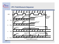
CPU Fetch/Execute Sequence
S1
S2
S3
S4
S5
S6
S1
S2
S3
S4
S5
S6
P1 P2 P1 P2 P1 P2 P1 P2 P1 P2 P1 P2 P1 P2 P1 P2 P1 P2 P1 P2 P1 P2 P1 P2
ALE
Read
Opcode
a)
b)
Read
Opcode (Discard)
S1
S2
S3
S4
S5
S6
1 Byte, 1 Cycle Instruction, e.g. INC A
Read
Read 2nd
Opcode
Byte
Read next Opcode again
Read next Opcode (Discard)
S1
S2
S3
S4
S5
1 Byte, 2 Cycle Instruction, e.g. INC DPTR
Dec 2000
Page 17
S1
S2
S3
MOVX (1 Byte, 2 Cycle)
S6
Read next
Opcode
(Discard)
Read
Opcode
d)
Read next
Opcode
S1
S2
S3
S4
S5
S6
2 Byte, 1 Cycle Instruction, e.g. ADD A, #Data
Read
Opcode
c)
1 External
Oscillator
Period
Read next Opcode
Again
S4
S5
S6
ADDR
S1
S2
S3
S4
S5
S6
Read next Opcode again
No Fetch
No Fetch
No ALE
S1
S2
DATA
S3
Access of External Memory
S4
S5
S6
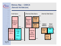
Memory Map -- C505CA
(Harvard Architecture)
(External) Data Space
Code Space
FFFFH
External
Data
Memory
External
EPROM
(32 k)
(XDATA)
8000H
External
EPROM
(32 k)
Internal
ROM/
OTP
Dec 2000
Page 18
(/EA = 1)
(1k Bytes)
FC00H
F7FF
F6FFH
External
Data
Memory
Indirect
Address
Direct
Address
Internal
RAM
SFR
(128 Bytes)
(128 Bytes)
Internal
RAM
(XDATA)
0000H
0000H
FFFFH
H
Internal
CAN Cntr.
(256 Bytes) F700H
7FFFH
(32 k)
(/EA = 0)
Internal
XRAM
(Internal) Data Space
(128 Bytes)
7FH
00H
FFH
80H
Memory Map (cont.)
Internal Data Space
7FH
Useful for Stack
Indirect
Address
Every 8th SFR
is Bit Addressable
Direct
Address
Scratch Pad RAM
FFH
Internal
RAM
(128 Bytes)
SFR
(128 Bytes) 80
H
Internal
RAM
(128 Bytes)
30H
7F 7E 7D 7C 7B 7A 79 78
7FH
Bit Addressable
Area
(128 bits)
00H
07 06 05 04 03 02 01 00
Direct and Indirect
Address
20H
Register Bank 3
Register Bank 2
Register Bank 1
Register Bank 0
Dec 2000
Page 19
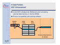
00H
8 Data Pointers
8051 Enhancement
Avoid 8051’s Datapointer Bottleneck when accessing
external data memory or internal XRAM
Ensure Compatibility with existing software
DPSEL
0092H
DPH
0083H
DPL
0082H
- - - - - .2 .1 .0
External Data Memory
Or XRAM
Dec 2000
Page 20
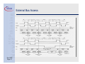
External Bus Access
Dec 2000
Page 21
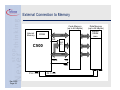
External Connection to Memory
Code Memory
(up to 64 kBytes)
Internal
Memory
XRAM
P2
A8-A15
Data Memory
(up to 64 kBytes)
without
XRAM
area
A8-A15
ALE
74HC
373
C500
P0
PSEN
A0-7
AD0-7
A0-A7
AD0-7
OE
WR
RD WR
P3.6 / WR
Dec 2000
Page 22
P3.7 / RD
Interrupt System
Interrupt Controller
– Short interrupt response time
– Context Switching
– Short interrupt service overhead
– Low total latency gives highest real-time performance
– Comprehensive prioritization scheme
Easy scheduling of complex real-time systems by using
up to 4 priority levels
Simultaneous interrupts of same priority undergo a
group-wise arbitration (using the inherent priority
structure)
Dec 2000
Page 23
Four Programmable Priority Levels
Ext. Int. 0
Highest
A/D Conv.
Group 0
Timer 0
CAN & SW
Lowest
Priority
Level
Group 1
Ext. Int. 3
Ext. Int. 1
Group 2
Ext. Int. 4
Timer 1
Group 3
Ext. Int. 5
USART
Group 4
Timer 2
Ext. Int. 6
Group 5
Dec 2000
Page 24
IP0
IP1
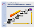
Inherent Priority Structure
- Only used for Simultaneous Interrupts of Same Priority
Ext. Int. 0
A/D
Conv.
Group 0
Timer 0
CAN &
SW
Ext. Int. 3
Ext. Int. 4
USART
Timer 1
Ext. Int. 1
High
Group 1
Group 2
Group 3
Ext. Int. 5
Ext. Int. 6
Timer 2
Group 5
Dec 2000
Page 25
Group 4
Low
High
Low
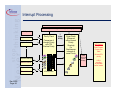
Interrupt Processing
Interrupt Control Register of the appropriate peripheral
INTR Flag is Set
Peripheral Interrupt
Peripheral Interrupt
Priority Check
Comparison of
Interrupt Priority
with CPU
Runtime Priority
if
higher
Priority
Group Check
(Placement
within Inherent
Priority
Structure)
For
Simultaneous
interrupts of
same Priority
INTR Service:
Push Program
Counter onto
Stack
Clear
INTR Flag
(not for
all flags)
Peripheral Interrupt
External Interrupt
Peripheral Interrupt
External Interrupt
Dec 2000
Page 26
4 Priority Levels
Set new CPU
priority
LCALL
according
to peripheral
vector number
Peripherals Set of the C505CA
2 Timer/Counter units (T0 & T1)
– 16 bit timers with 4 operating modes (including 1 reload mode)
A 3rd 16 bit Timer/Counter with 4 Channel Capture Compare
– 2 Capture Modes and 2 Compare Modes
Independent Full Duplex USART
– 3 Asynchronous modes, 1 Synchronous mode
– Dedicated Baudrate Generator
8 channel 10-Bit A/D Converter
Full CAN Controller
– Conforms to CAN 2.0B Active specification
– 15 Message Object
– Up to 1Mb/s
Watchdog: 15-bit Reload-timer causes reset on overflow
Dec 2000
Page 27
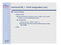
C505CA Hands-On Peripheral Training
Exercise Overview
How to set up the
Hardware and Software
Peripherals in Detail +
Exercises
– Timer/Counter 0
– Timer/Counter 1
– USART
– A/D Converter
– Timer 2
– CAN Module
Dec 2000
Page 28
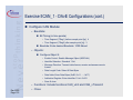
Exercise Overview
Exercise for USART and T0/T1:
– 5URT_1 - Asynchronous Serial Transmission of data
periodically
– 5URT_2 - Synchronous Serial Transmission of data periodically
Exercise for Timer 2 (CAPTURE/COMPARE UNIT):
– 5T2_1 -
PWM using Timer 2
– 5T2_2 -
Signal Generation / Signal Detection with
Timer 2*
Exercise for the Analog to Digital Converter:
– 5ADC_1 - Control the Pulse Width of a PWM signal with an
ADC Value (using the ADC ISR)**
Exercise for the CAN Module:
– 5CAN_1 - Transmit a standard CAN Message with the
On-Chip CAN Module (C505C and C505CA only)
Dec 2000
Page 29
* Requires External Connections
** Requires External Connections and Components
Hints regarding the Exercises
Exercise numbering scheme:
– Generally the exercise name contains the starter kit, the
peripheral the exercise was mainly designed for and a
running number
– Exercise “5URT_2” would be the 2nd example for the
USART using the kitCON-505C Starter Kit
To create a new exercise:
– For each exercise, use a different subdirectory
c:\hot505CA_1\newex (e.g. c:\hot505CA_1\5URT_1)
Dec 2000
Page 30
System Setup:
Directory Structure
Create a subdirectory on your hard drive:
c:\hotC505CA_1
Create the following subdirectories on you hard drive to
store the project and code for each of the exercises:
c:\hot505CA_1\5URT_1
c:\hot505CA_1\5URT_2
c:\hot505CA_1\5T2_1
c:\hot505CA_1\5T2_2
c:\hot505CA_1\5ADC_1
c:\hot505CA_1\5CAN_1
Dec 2000
Page 31
Tool/Project Flow
µVision2
DAvE
C Code
Dec 2000
Page 32
Keil
Compiler/
Linker
Hex Code
Keil
Debugger
Phytec
Evaluation
Board
Oscilloscope
System Setup:
kitCON-505C Hardware Setup
Make sure that all jumpers are in their default positions
as described in the KitCON-505C Hardware-Manual.
Make sure that jumper JP11 is open.
Attach only an unregulated power supply with 8V to 12V
/500 mA to X2 on the KitCON-505C. Double check the
correct polarity!
Connect your Starter Kit board to your IBM compatible
PC using a serial cable (connector X4 to COM1 - X4 is
the connector closest to the RESET button on the board)
NOTE: These examples assume that the KitCON-505C is
equipped with a 16 MHz crystal. Earlier editions of the
board may have slower crystals. This will effect the
timing of periodic interrupts, and some of the settings in
DAvE.
Dec 2000
Page 33
System Setup:
kitCON-505C Hardware Setup (cont.)
The Keil Monitor Program MUST be programmed into
the Flash of the kitCON-505C
– The Keil Monitor is programmed into the Flash on all
boards by default. If the flash is erased or reprogrammed, the Monitor will need to be re-programmed
– Use the Phytec FlashTools to program the Keil Monitor
(mon505.hex) into the Flash
See the KitCON-505C Hardware Manual for details on
programming the kitCON-505C Flash.
If your board has a C505C device, you should replace it
with a C505CA.
– Be careful when opening the socket on the board. The
socket is easily damaged.
Dec 2000
Page 34
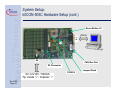
System Setup:
kitCON-505C Hardware Setup (cont.)
Reset Button S1
P1
RS232
X5
CAN Bus Port
X3 Connector
C505CA
8V-12V DC / 500mA
Tip: Inside “+”, Outside: “-”
Dec 2000
Page 35
Jumper Block
System Setup:
kitCON-505C Hardware Setup (cont.)
X3
You need this
page when you
do the
exercises...
Dec 2000
Page 36
System Setup:
Intall DAvE 2.1 (If you haven’t already)
Insert the DAvE 2.1 CD in your CD ROM drive.
Run CD ROM\Setup.exe.
Follow the setup program’s instructions.
– Install the microcontrollers you’d like to work with. You can
always re-install or delete derivatives later on.
– Be sure to install the Smart Search.
– If you’d like to get a detailed introduction to DAvE 2.1, be sure to
include the tutorial. You can delete it afterwards to free up space.
If you don’t have Acrobat Reader installed on your PC, do so
by choosing to install Acrobat Reader which is included on the
DAvE CD.
(Hint: You need Acrobat Reader 4.0 or higher)
Please note:
You need WINDOWS 95 or later or WINDOWS NT in order to
run DAvE!
Dec 2000
Page 37
System Setup:
Install Keil µVision2
Most of the Starter Kit CDROMs contain an old version
of µVision.
Please go to the Keil web-site (www.keil.com) and
download the latest Keil 8051 evaluation tools.
Please Note:
The Evaluation version of the Tools is restricted to 2k of
Code. The Code will be located at address 0x4000.
Dec 2000
Page 38
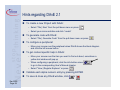
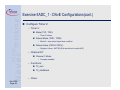
Hints regarding DAvE 2.1
To create a new Project with DAvE:
– Select “File | New” from the pull down menu or press
– Select your microcontroller and click “create”
To generate code with DAvE:
– Select “File | Generate Code” from the pull down menu or press
To configure a peripheral:
– Move your mouse over the peripheral when DAvE shows the block diagram
and click the left mouse button
To get context specific help in DAvE:
– Move your mouse over the item you want to find out about, sometimes a
yellow text window will pop up
– When configuring a peripheral, click the info-button arrow
to go to the corresponding User’s Manual chapter
– Select “View | Register Explorer” or press
Validate each alpha numeric entry by pressing ENTER
To save & close any DAvE window, click
Dec 2000
Page 39
or
Hints regarding the Exercises
The exercises are created in a way that they use only
peripherals which have been introduced already (either
directly before the exercise or in previous exercises)
If an exercise does not work when running the
debugger:
– Check the oscilloscope connections (right pin?)
– Check the DAvE / µVision configurations
– Re-generate the code with DAvE (USER CODE remains!)
– Recompile the exercise in µVision
– Reload the exercise into the debugger and run it again
– The debugger may appear to react slowly when using
Windows NT
Dec 2000
Page 40
Let’s
Let’s get
get
started
started now!
now!
Dec 2000
Page 41
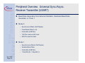
Peripheral Overview: Universal Sync./Async.
Receiver Transmitter (USART)
Baud Rate Generation from External Oscillator, Dedicated Baud Rate
Generator, or Timer 1
Mode 0
– Synchronous Mode (Half Duplex)
– Fixed Baud Rate (fosc/6)
– 8 data bits (LSB first)
– TxD Pin used as shift clock
– RxD Pin used for data
Mode 1
– Asynchronous Mode (Full Duplex)
– Variable Baud Rate
– 8 data bits (LSB first)
– 1 Start Bit (0); 1 Stop Bit (1)
Dec 2000
Page 42
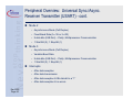
Peripheral Overview: Universal Sync./Async.
Receiver Transmitter (USART) - cont.
Mode 2
– Asynchronous Mode (Full Duplex)
– Fixed Baud Rate (fosc/16 or fosc/32)
– 9 data bits (LSB first) -- Parity, Multiprocessor Communication
– 1 Start Bit (0); 1 Stop Bit (1)
Mode 3
– Asynchronous Mode (Full Duplex)
– Variable Baud Rate
– 9 data bits (LSB first) -- Parity, Multiprocessor Communication
– 1 Start Bit (0); 1 Stop Bit (1)
Interrupts
– After data reception
– After data transmission
– After data reception & 9th data bit is a “1”
– After data reception & no errors
Dec 2000
Page 43
USART Function Diagram
SM0
SRELH SRELL
fosc
SM1
Baud
Rate
Clock
BD
Mode 1
Mode 3
10-Bit Timer
÷2
÷16
Timer 1 Overflow
fosc
Mode 2
÷6
SMOD
Mode 0
3 to 2
MUX
SBUF
∇
SBUF
Shift Reg
TxD
Shift Reg
RxD
Control/Timing/Mode
Logic
Baud Rate Clock
Dec 2000
Page 44
SCON
TI
RI
>1
Interrupt
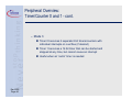
Peripheral Overview:
Timer/Counter 0 and 1
2 separate 16 Bit Timers/Counters
– Timer when clocked by external oscillator (fosc ÷ 6)
– Counter when clocked by external pin (P3.4/T0 or P3.5/T1)
– Can measure pulse widths when used as a “Gated Timer”
Clocked by external oscillator when P3.2/INT0 or P3.3/INT1 is high
4 Operating Modes
– Mode 0
8 bit timer/counter with 5 bit (divide by 32) prescaler
Interrupt on rollover (if desired)
– Mode 1
16 bit timer/counter
Interrupt on rollover (if desired)
– Mode 2
8 bit timer with 8 bit reload on overflow
Interrupt on rollover (if desired)
Dec 2000
Page 45
Peripheral Overview:
Timer/Counter 0 and 1 - cont.
– Mode 3
Timer 0 becomes 2 separate 8 bit timers/counters with
individual interrupts on overflow (if desired)
Timer 1 becomes a 16 bit timer that can be started and
stopped at any time, but cannot cause an interrupt
Useful when an “extra” timer is needed
Dec 2000
Page 46
Timer/Counter 0 and 1 Operating Modes
Osc
MODE 0
P3.4/T0
or
P3.5/T1
÷6
TR0 or TR1
THx
TLx
(8 bits) (5 bits)
TFx
THx
TLx
(8 bits) (8 bits)
TFx
Interrupt
C/T
Gate
P3.2/INT0
or
P3.3/INT1
Osc
MODE 1
P3.4/T0
or
P3.5/T1
TR0 or TR1
Gate
Dec 2000
Page 47
÷6
P3.2/INT0
or
P3.3/INT1
C/T
Interrupt
Timer/Counter 0 and 1 Operating Modes (cont.)
Osc
MODE 2
P3.4/T0
or
P3.5/T1
÷6
TR0 or TR1
TLx
(8 bits)
C/T
Gate
MODE 3
P3.4/T0
TR0
Reload
THx
(8 bits)
P3.2/INT0
or
P3.3/INT1
Osc
TR1
TH0
(8 bits)
÷6
TL0
(8 bits)
TF1
TF0
C/T
Gate
P3.2/INT0
TH1
TL1
(8 bits) (8 bits)
M0 M1
Dec 2000
Page 48
TFx
Interrupt
Interrupt
Interrupt
Exercise 5URT_1 - Periodic Asynchronous Serial
Data Transmission - Description
Objective: Send asynchronous serial data periodically
using the USART and Timer 0
– Period: 1 overflow of Timer 0 in mode 0 (3.072 ms with a
16 MHz crystal)
– Data: Send constant data (0x55) at a baud rate of 9600
– Use USART mode 1 (8 data bits, 1 start bit, 1 stop bit,
variable baud rate)
Dec 2000
Page 49
Exercise 5URT_1 - DAvE Configurations
Start DAvE 2.1
Select “Create a new project” from the Startup Dialog or click
Select the 8-Bit microcontroller C505CA and click “Create”
(if this microcontroller is not on the list, you need to re-install it
from the DAvE 2.1 CD ROM)
DAvE will create the project
Save your project by selecting “File | Save” or press
– Browse to directory “c:\hot505CA_1\5URT_1\”
– Enter project name: “5URT_1”
– Click “Save”
You will see the C505CA block diagram and the Project
Settings Window (configuration see next slide)
To get back to the Project Settings window in case you close
it: Select “File | Project Settings”
Dec 2000
Page 50
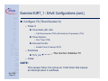
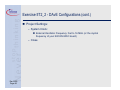
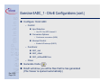
Exercise 5URT_1 - DAvE Configurations (cont.)
Project Settings:
– System Clock:
External Oscillator Frequency: Set to 16 MHz (or the crystal
frequency of your KitCON-505C board)
– Close
NOTE:
By default, DAvE enables access to the CAN controller
and XRAM
Dec 2000
Page 51
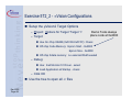
Exercise 5URT_1 - DAvE Configurations (cont.)
Configure T0 (Timer/Counter 0):
– Timer 0
Timer Mode (M1, M0):
– 8 bit timer/counter (TH0) with divide-by-32 prescaler (TL0)
Timer Options:
– Run Timer (TR0)
Interrupt Control:
– Enable Timer 0 interrupt (ET0)
– Functions
T01v_Init
This function Initializes T0
– Close
NOTE:
This causes Timer 0 to act as an 13-bit timer that causes
an interrupt when it overflows
Dec 2000
Page 52
Exercise 5URT_1 - DAvE Configurations (cont.)
Configure 8-Bit USART
– Control:
Global:
– Use TXD (P3.1) for serial Channel
Mode Control (SM0, SM1)
– Mode 1: 8-bit data, 1 startbit, 1 stopbit, variable baudrate (async)
Baudrate Clock Source
– Use the Internal Baud Rate Generator
– Divide by 2 (optional)
Baudrate
– Required Baudrate = 9600
– Functions
USART_vInit
This function Initializes the USART
USART_vSendData
– Close
Generate Code (
We will use this function to transmit data
)
DAvE will show you all the files that he has generated
(File Viewer is opened automatically)
Dec 2000
Page 53
Exercise 5URT_1 - µVision2 Configurations
Start Keil µVision2
NOTE:
µVision2 is able to read the DAvE project settings
(contained in the .dpt file) and automatically create a
µVision2 project. µVision2 will also automatically
generate the assembly startup file!
Create the new Project by opening the DAvE .dpt file
– Project: Open Project:
c:\hot505CA_1\5URT_1\5URT_1.dpt
Dec 2000
Page 54
Exercise 5URT_1 - µVision2 Configurations (cont.)
Setup the µVision2 Target Options
– Project: Options for Target ‘Target 1’:
– Target:
Demo Tools always
place code at 0x4000
Use On-Chip XRAM (0xFC00-0xFFFF): Check
Off-chip Code Memory: Eprom Start - 0x4000
Eprom Size - 0x4000
Off-chip Xdata memory: no external RAM needed
– Debug:
Use: Keil Monitor-51 Driver - select
Load Application at Startup - check
– Click OK
Use the tree to open all .c files
Dec 2000
Page 55
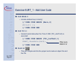
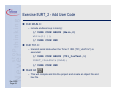
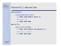
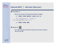
Exercise 5URT_1 - Add User Code
Edit MAIN.C:
– include endless loop in main():
// USER CODE BEGIN (Main,2)
while(1) {};
// USER CODE END
Edit T01.C:
– transmit serial data when the Timer 0 ISR (T01_viIsrTmr0) is
executed:
// USER CODE BEGIN (T01_IsrTmr0,1)
USART_vSendData(0x55);
// USER CODE END
This is an
ASCII ‘U’
Build All
– This will compile and link the project and create an object file and
hex file.
Dec 2000
Page 56
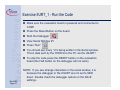
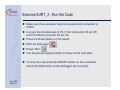
Exercise 5URT_1 - Run the Code
Make sure the evaluation board is powered and connected to
COM1
Press the Reset Button on the board
Start the Debugger
View Serial Window #1
Press “Run”
You should see many “U”s being written in the Serial window.
This is data sent by the C505CA to the PC via the USART!
To stop the code press the RESET button on the evaluation
board (the Halt button on the debugger will not work).
Dec 2000
Page 57
NOTE: If you see strange characters in the serial window, it is
because the debugger or the USART are not set to 9600
baud. Double check the debugger options or the DAvE
settings.
Exercise 5URT_2 - Periodic Synchronous Serial
Data Transmission - Description
Objective: Send synchronous serial data periodically
using the USART and Timer 1
– Period: 16 Timer 1 counts
Timer 1 in mode 2
– Reload value of 0xF0 overflow of Timer 1 in mode 0 (6 µs with a
16 MHz crystal)
– Data: Send constant data (0xAA)
– Use USART mode 0
8 data bits
Fixed Baud Rate
– 1/6 external oscillator frequency
– 2.666 Mb/s (@ 16 MHz)
Dec 2000
Page 58
Exercise 5URT_2 - DAvE Configurations
Start DAvE 2.1
Select “Create a new project” from the Startup Dialog or click
Select the 8-Bit microcontroller C505CA and click “Create”
(if this microcontroller is not on the list, you need to re-install it
from the DAvE 2.1 CD ROM)
DAvE will create the project
Save your project by selecting “File | Save” or press
– Browse to directory “c:\hot505CA_1\5URT_2\”
– Enter project name: “5URT_2”
– Click “Save”
You will see the C505CA block diagram and the Project
Settings Window (configuration see next slide)
To get back to the Project Settings window in case you close
it: Select “File | Project Settings”
Dec 2000
Page 59
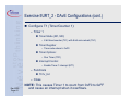
Exercise 5URT_2 - DAvE Configurations
Project Settings:
– System Clock:
External Oscillator Frequency: Set to 16 MHz (or the crystal
frequency of your KitCON-505C board)
– Close
Dec 2000
Page 60
Exercise 5URT_2 - DAvE Configurations (cont.)
Configure T1 (Timer/Counter 1):
– Timer 1
Timer Mode (M1, M0):
– 8 bit timer/counter (TL1) with 8-bit auto-reload (TH1)
Timer Register
– Timer auto-reload = 0xF0
Timer Options:
– Run Timer (TR1)
Interrupt Control:
– Enable Timer 1 interrupt (ET1)
– Functions
T01v_Init
– Close
Dec 2000
Page 61
NOTE: This causes Timer 1 to count from 0xF0 to 0xFF
and cause an interrupt when it overflows.
Exercise 5URT_2 - DAvE Configurations (cont.)
Configure 8-Bit USART
– Control:
Global:
– Use TXD (P3.1) for serial Channel
Mode Control (SM0, SM1)
– Mode 0: 8-bit Shift register, fixed baud rate (sync)
– Functions
USART_vInit
USART_vSendData
– Close
Generate Code (
)
DAvE will show you all the files that he has generated
(File Viewer is opened automatically)
Dec 2000
Page 62
Exercise 5URT_2 - µVision2 Configurations
Start Keil µVision2
NOTE:
µVision2 is able to read the DAvE project settings
(contained in the .dpt file) and automatically create a
µVision2 project. µVision2 will also automatically
generate the assembly startup file!
Create the new Project by opening the DAvE .dpt file
– Project: Open Project:
c:\hot505CA_1\5URT_2\5URT_2.dpt
Dec 2000
Page 63
Exercise 5URT_2 - µVision2 Configurations (cont.)
Setup the µVision2 Target Options
– Project: Options for Target ‘Target 1’:
– Target:
Demo Tools always
place code at 0x4000
Use On-Chip XRAM (0xFC00-0xFFFF): Check
Off-chip Code Memory: Eprom Start - 0x4000
Eprom Size - 0x4000
Off-chip Xdata memory: no external RAM needed
– Debug:
Use: Keil Monitor-51 Driver - select
Load Application at Startup - check
– Click OK
Use the tree to open all .c files
Dec 2000
Page 64
Exercise 5URT_2 - Add User Code
Edit MAIN.C:
– include endless loop in main():
// USER CODE BEGIN (Main,2)
while(1) {};
// USER CODE END
Edit T01.C:
– transmit serial data when the Timer 1 ISR (T01_viIsrTmr1) is
executed:
// USER CODE BEGIN (T01_IsrTmr1,1)
USART_vSendData(0xAA);
// USER CODE END
Build All
– This will compile and link the project and create an object file and
hex file.
Dec 2000
Page 65
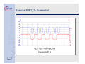
Exercise 5URT_2 - Run the Code
Make sure the evaluation board is powered and connected to
COM1
Connect the Oscilloscope to P3.1/TxD (connector X3 pin 97)
and P3.0/RxD (connector X3 pin 93)
Press the Reset Button on the board
Start the Debugger
Press “Run”
You should see signals similar to those on the next slide
To stop the code press the RESET button on the evaluation
board (the Halt button on the debugger will not work).
Dec 2000
Page 66
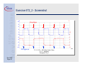
Exercise 5URT_2 - Screenshot
V
10
8
6
4
2
0
-2
-4
-6
-8
-10
Dec 2000
Page 67
V
-2
-1
0
1
2
3
4
5
P3.1 / TxD -- Shift Clock (Top)
P3.0 / RxD -- Data (Bottom)
Example 5URT_2
6
7
10
8
6
4
2
0
-2
-4
µs
Timer 2 with 4 Channel Capture/Compare Unit
16 bit Timer/Counter
– In Timer mode the timer increments at fosc/6 or fosc/12
– In Counter mode the timer increments every falling edge
of P1.7/T2
– In Gated Timer mode the timer increments at fosc/6 or
fosc/12 when P1.7/T2 is high (good for pulse width
measurement)
4 Channel Capture/Compare Module
– 4 16-bit registers can hold capture or compare values
In capture modes, the registers will latch the timer value in
response to external pin transitions (or software)
In compare modes, pin transitions occur when the timer
reaches the register value (PWM generation)
One of the channels can be used as a 16-bit reload value for
the timer
Dec 2000
Page 68
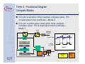
Timer 2 - Functional Overview
CC0
CC1
16-bit General Purpose
Timer/Counter Unit
∇
Dec 2000
Page 69
Comparator
∇
Comparator
CAP/COM/Reload
CAP/COM Reg
(CRCL/CRCH)
(CCL1/CCH2)
I/O Pin
Control CC2
CC3
∇
Comparator
CAP/COM Reg
(CCL2/CCH2)
∇
Comparator
CAP/COMReg
(CCL3/CCH3)
Timer 2 - Functional Diagram
16 bit Timer Unit
T2I0
4 to 1
Mux
T2
P1.7
fosc
&
÷6
3 to 1
Mux
÷12
T2R0,
T2EX
P1.5
Dec 2000
Page 70
T2PS
T2R1
T2I1
Timer 2 (16-bit)
TL2
TH2
∆
CRCL
TF2
>1
CRCH
EXF2
Interrupt
Request
Timer 2 - Functional Diagram
Capture Modes
Mode 0
– Timer Contents Captured on positive edge of CCx Pin
(CC0 can capture on positive or negative edge)
Mode 1
– Timer Contents can be captured by a write (dummy value)
to the low byte of the capture/compare register -- Mode 1
Interrupt
Request
CC1
CC2
CC3
IEXx
Timer 2
TL2
TH2
CC0
∇
I3FR
Dec 2000
Page 71
Channel 0
Only
COCALx COCAHx
Write to
Low Byte
CCLx
CCHx
OR
CRCL
CRCH
Timer 2 - Functional Diagram
Compare Modes
CCx pin is set when timer reaches compare value. Pin
is reset when timer overflows -- Mode 0
CCx pin is either set or reset when timer reaches
compare value. Pin is reset when timer overflows -Mode 1
I3FR
IEXx
Interrupt
Request
Timer Value
Compare Value
CRCL
CRCH
Output
Pin 1.x/CCx
OR
CCHx
S
R
16-bit Compare
TL2
Dec 2000
Page 72
TH2
Q
Mode 0
Flip-Flop
P1.x
Overflow
CCx
∇
CCLx
shadow
T2CM
Channel 0
Only
Mode 1
Only
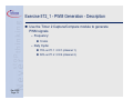
Exercise 5T2_1 - PWM Generation - Description
Use the Timer 2 Capture/Compare module to generate
PWM signals
– Frequency:
10 kHz
– Duty Cycle:
75% on P1.1 / CC1 (channel 1)
50% on P1.2 / CC2 (channel 2)
Dec 2000
Page 73
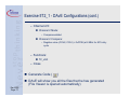
Exercise 5T2_1 - DAvE Configurations
Start DAvE 2.1
Select “Create a new project” from the Startup Dialog or click
Select the 8-Bit microcontroller C505CA and click “Create”
(if this microcontroller is not on the list, you need to re-install it
from the DAvE 2.1 CD ROM)
DAvE will create the project
Save your project by selecting “File | Save” or press
– Browse to directory “c:\hot505CA_1\5T2_1\”
– Enter project name: “5T2_1”
– Click “Save”
You will see the C505CA block diagram and the Project
Settings Window (configuration see next slide)
To get back to the Project Settings window in case you close
it: Select “File | Project Settings”
Dec 2000
Page 74
Exercise 5T2_1 - DAvE Configurations (cont.)
Project Settings:
– System Clock:
External Oscillator Frequency: Set to 16 MHz (or the crystal
frequency of your KitCON-505C board)
– Close
Dec 2000
Page 75
Exercise 5T2_1 - DAvE Configurations (cont.)
Configure Timer 2:
– Timer 2:
Mode (T2I1, T2I0):
– Timer Function
Reload Mode (T2R1, T2R0):
– Mode 0: auto-reload upon timer overflow
Reload Value (CRCH, CRCL):
– Register Value = 0xFEF5 (at 16 MHz for 10kHz frequency)
– Channel 0/1:
Channel 1 Mode:
– Compare enabled
Channel 1 Compare:
– Register value (CCH1, CCL1) = 0xFF37 (at 16 MHz for 75%
duty cycle)
Dec 2000
Page 76
Exercise 5T2_1 - DAvE Configurations (cont.)
– Channel 2/3:
Channel 2 Mode:
– Compare enabled
Channel 2 Compare:
– Register value (CCH2, CCL2) = 0xFF99 (at 8 MHz for 50% duty
cycle
– Functions:
T2_vInit
– Close
Generate Code (
)
DAvE will show you all the files that he has generated
(File Viewer is opened automatically)
Dec 2000
Page 77
Exercise 5T2_1 - µVision2 Configurations
Start Keil µVision2
NOTE:
µVision2 is able to read the DAvE project settings
(contained in the .dpt file) and automatically create a
µVision2 project. µVision2 will also automatically
generate the assembly startup file!
Create the new Project by opening the DAvE .dpt file
– Project: Open Project:
c:\hot505CA_1\5T2_1\5T2_1.dpt
Dec 2000
Page 78
Exercise 5T2_1 - µVision2 Configurations (cont.)
Setup the µVision2 Target Options
– Project: Options for Target ‘Target 1’:
– Target:
Demo Tools always
place code at 0x4000
Use On-Chip XRAM (0xFC00-0xFFFF): Check
Off-chip Code Memory: Eprom Start - 0x4000
Eprom Size - 0x4000
Off-chip Xdata memory: no external RAM needed
– Debug:
Use: Keil Monitor-51 Driver - select
Load Application at Startup - check
– Click OK
Use the tree to open all .c files
Dec 2000
Page 79
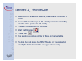
Exercise 5T2_1 - Add User Code
Edit MAIN.C:
– include endless loop in main():
// USER CODE BEGIN (Main,2)
while(1) {};
// USER CODE END
Build All
– This will compile and link the project and create an object
file and hex file.
Dec 2000
Page 80
Exercise 5T2_1 - Run the Code
Make sure the evaluation board is powered and connected to
COM1
Connect the Oscilloscope to P1.1/CC1 (connector X3 pin 89)
and P1.1/CC2 (connector X3 pin 86)
Press the Reset Button on the board
Start the Debugger
Press “Run”
You should see signals similar to those on the next slide
To stop the code press the RESET button on the evaluation
board (the Halt button on the debugger will not work).
Dec 2000
Page 81
Exercise 5T2_1 - Screenshot
V
10
V
8
6
4
2
10
0
8
-2
6
-4
4
-6
2
-8
0
-10
0
Dec 2000
Page 82
20
40
60
80
100
120
140
P1.1 / CC1 -- 75% Duty Cycle (Top)
P1.2 / CC2 -- 50 % Duty Cycle (Bottom)
Example 5T2_1
160
180
-2
200 µs
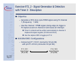
Exercise 5T2_2 - Signal Generation & Detection
with Timer 2 - Description
Objective
– Generate a 50% duty cycle PWM signal using T2 channel
1 (Frequency: 1 kHz)
– Use the channel 1 PWM signal (rising edge) to trigger a
T2 capture event on channel 2 and cause an interrupt.
Timer 2 contents will be written automatically to channel 2
Capture/Compare register (CCH2 and CCL2)
Use the capture ISR to toggle pin P1.4
KitCON-505C Configurations:
– Connect pin P1.1/CC1 (connector X3 pin 89)
with pin P1.2/CC2 (connector X3 pin 86):
P1.1 / CC1
Signal Output
(X3 pin 89)
Dec 2000
Page 83
P1.2 / CC2
Signal Detection
(X3 pin 86)
Exercise 5T2_2 - DAvE Configurations
Start DAvE 2.1
Select “Create a new project” from the Startup Dialog or click
Select the 8-Bit microcontroller C505CA and click “Create”
(if this microcontroller is not on the list, you need to re-install it
from the DAvE 2.1 CD ROM)
DAvE will create the project
Save your project by selecting “File | Save” or press
– Browse to directory “c:\hot505CA_1\5T2_2\”
– Enter project name: “5T2_2”
– Click “Save”
You will see the C505CA block diagram and the Project
Settings Window (configuration see next slide)
To get back to the Project Settings window in case you close
it: Select “File | Project Settings”
Dec 2000
Page 84
Exercise 5T2_2 - DAvE Configurations (cont.)
Project Settings:
– System Clock:
External Oscillator Frequency: Set to 16 MHz (or the crystal
frequency of your KitCON-505C board)
– Close
Dec 2000
Page 85
Exercise 5T2_2 - DAvE Configurations (cont.)
Configure Timer 2:
– Timer 2:
Mode (T2I1, T2I0):
– Timer Function
Reload Mode (T2R1, T2R0):
– Mode 0: auto-reload upon timer overflow
Reload Value (CRCH, CRCL):
– Register Value = 0xF596 (at 16 MHz for 1kHz frequency)
– Channel 0/1:
Channel 1 Mode:
– Compare enabled
Channel 1 Compare:
– Register value (CCH1, CCL1) = 0xFACB (at 16 MHz for 50%
duty cycle)
Dec 2000
Page 86
Exercise 5T2_2 - DAvE Configurations (cont.)
– Channel 2/3:
Channel 2 Mode:
– Capture on rising edge at pin P1.2 / CC2
Channel 2 Interrupt:
– Enable CC2 interrupt
– Functions:
T2_vInit
– Close
Generate Code (
)
DAvE will show you all the files that he has generated
(File Viewer is opened automatically)
Dec 2000
Page 87
Exercise 5T2_2 - µVision Configurations
Start Keil µVision2
NOTE:
µVision2 is able to read the DAvE project settings
(contained in the .dpt file) and automatically create a
µVision2 project. µVision2 will also automatically
generate the assembly startup file!
Create the new Project by opening the DAvE .dpt file
– Project: Open Project:
c:\hot505CA_1\5T2_2\5T2_2.dpt
Dec 2000
Page 88
Exercise 5T2_2 - µVision Configurations
Setup the µVision2 Target Options
– Project: Options for Target ‘Target 1’:
– Target:
Demo Tools always
place code at 0x4000
Use On-Chip XRAM (0xFC00-0xFFFF): Check
Off-chip Code Memory: Eprom Start - 0x4000
Eprom Size - 0x4000
Off-chip Xdata memory: no external RAM needed
– Debug:
Use: Keil Monitor-51 Driver - select
Load Application at Startup - check
– Click OK
Use the tree to open all .c files
Dec 2000
Page 89
Exercise 5T2_2 - Add User Code
Edit MAIN.C:
– include endless loop in main():
// USER CODE BEGIN (Main,2)
while(1) {};
// USER CODE END
Edit T2.C:
– define P1.4 as an SFR bit
// USER CODE BEGIN (T2_General,1)
sbit P1_4 = P1^4;
// USER CODE END
Dec 2000
Page 90
Exercise 5T2_2 - Add User Code (cont.)
– toggle pin P1.4 in the channel 2 capture ISR:
// USER CODE BEGIN (T2_IsrEx5,1)
P1_4 = !P1_4;
// USER CODE END
Build All
– This will compile and link the project and create an object
file and hex file.
Dec 2000
Page 91
Exercise 5T2_2 - Run the Code
Make sure the evaluation board is powered and connected to
COM1
Connect the Oscilloscope to P1.1/CC1 (connector X3 pin 89)
and P1.4 (connector X3 pin 87)
Press the Reset Button on the board
Start the Debugger
Press “Run”
You should see signals similar to those on the next slide
To stop the code press the RESET button on the evaluation
board (the Halt button on the debugger will not work).
Dec 2000
Page 92
Exercise 5T2_2 - Screenshot
10
V
V
Rising Edges
8
6
4
2
10
0
8
-2
6
-4
4
-6
2
-8
0
-10
-2
ISR toggles pin
Dec 2000
Page 93
ms
P1.1 / CC1 -- 50% Duty Cycle (Top)
P1.4 -- (Bottom)
Example 5T2_2
Analog-to-Digital Converter
8 channel multiplexed input
Programmable conversion time
10 bit resolution
6 µsec minimum conversion time
Internal Capture and Hold circuit
Single or Continuous conversion modes
Busy Flag
End of Conversion interrupt
Dec 2000
Page 94
Analog-to-Digital Converter Functional Diagram
VAREF
VAGND
ADCON0 & ADCON1
MX2
MX1
ADCON0
MX0
ADM
Port 1
Sample
&
Hold
8 to 1
Mux
fOSC
Clock Prescaler
÷32, 16, 8, 4
ADCL1
ADCL0
ADCON1
Dec 2000
Page 95
Conversion Clock
10-Bit
Analog
To
Digital
Converter
Single / Continuous Mode
ADDATH
ADDATL
Start of Conversion (dummy byte)
(2 MHz max.)
BSY
IADC
IRCON
(Conversion Complete Interrupt)
ADCON0
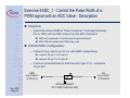
Exercise 5ADC_1 - Control the Pulse Width of a
PWM signal with an ADC Value - Description
Objective:
– Control the Pulse Width of Timer 2 channel 1 from approximately
0% to 100% with an ADC Value from the ADC channel 0.
ADC will be placed in “Continuous Conversion Mode”
ADC ISR will update the PWM duty cycle
KitCON-505C Configuration:
– Connect VAREF and VAGND to VCC and GND (respectively)
connect X3 pin 1 to X3 pin 61
connect X3 pin 3 to X3 pin 62
– Connect a potentiometer to A/D channel 0 (pin P1.0 - connector
X3 pin 69)
GND
(e.g. X3 pin 3
or X3 pin 4)
Dec 2000
Page 96
Vcc
(e.g. X3 pin 1
or X3 pin 2)
A/D input channel 0
P1.0 / AN0 (X3 pin 69 or 85)
Exercise 5ADC_1 - DAvE Configurations
Start DAvE 2.1
Select “Create a new project” from the Startup Dialog or click
Select the 8-Bit microcontroller C505CA and click “Create”
(if this microcontroller is not on the list, you need to re-install it
from the DAvE 2.1 CD ROM)
DAvE will create the project
Save your project by selecting “File | Save” or press
– Browse to directory “c:\hot505CA_1\5ADC_1\”
– Enter project name: “5ADC_1”
– Click “Save”
You will see the C505CA block diagram and the Project
Settings Window (configuration see next slide)
To get back to the Project Settings window in case you close
it: Select “File | Project Settings”
Dec 2000
Page 97
Exercise 5ADC_1 - DAvE Configurations (cont.)
Project Settings:
– System Clock:
External Oscillator Frequency: Set to 16 MHz (or the crystal
frequency of your KitCON-505C board)
– Close
Dec 2000
Page 98
Exercise 5ADC_1 - DAvE Configurations(cont.)
Configure Timer 2:
– Timer 2:
Mode (T2I1, T2I0):
– Timer Function
Reload Mode (T2R1, T2R0):
– Mode 0: auto-reload upon timer overflow
Reload Value (CRCH, CRCL):
– Register Value = 0xFF00 (8 bit resolution to match A/D)
– Channel 0/1:
Channel 1 Mode:
– Compare enabled
– Functions:
T2_vInit
T2_vSetMatch
– Close
Dec 2000
Page 99
Exercise 5ADC_1 - DAvE Configurations (cont.)
Configure 10-bit ADC:
– Control:
Input Selection:
– Use P1.0 for ADC channel 0
Conversion Options:
– Continuous conversion (ADM)
Interrupt Control:
– Enable A/D interrupt (EADC)
– Functions:
ADC_vInit
ADC_vStart
ADC_ubRead8BitConv
– Close
Generate Code (
Dec 2000
Page 100
)
DAvE will show you all the files that he has generated
(File Viewer is opened automatically)
Exercise 5ADC_1 - µVision Configurations
Start Keil µVision2
NOTE:
µVision2 is able to read the DAvE project settings
(contained in the .dpt file) and automatically create a
µVision2 project. µVision2 will also automatically
generate the assembly startup file!
Create the new Project by opening the DAvE .dpt file
– Project: Open Project:
c:\hot505CA_1\5ADC_1\5ADC_1.dpt
Dec 2000
Page 101
Exercise 5ADC_1 - µVision Configurations (cont.)
Setup the µVision2 Target Options
– Project: Options for Target ‘Target 1’:
– Target:
Demo Tools always
place code at 0x4000
Use On-Chip XRAM (0xFC00-0xFFFF): Check
Off-chip Code Memory: Eprom Start - 0x4000
Eprom Size - 0x4000
Off-chip Xdata memory: no external RAM needed
– Debug:
Use: Keil Monitor-51 Driver - select
Load Application at Startup - check
– Click OK
Use the tree to open all .c files
Dec 2000
Page 102
Exercise 5ADC_1 - Add User Code
Edit MAIN.C:
– start A/D converter and include endless loop in main():
// USER CODE BEGIN (Main,2)
ADC_vStart(CHANNEL_0, ADC_MODE_CONT);
while(1) {};
// USER CODE END
Dec 2000
Page 103
Exercise 5ADC_1 - Add User Code (cont.)
Edit ADC.C:
– Move A/D result to the Capture/Compare register
// USER CODE BEGIN (ADC_Isr,0)
T2_vSetMatch(1, 0xFF00 |
ADC_ubRead8BitConv());
// USER CODE END
Build All
– This will compile and link the project and create an object
file and hex file.
Dec 2000
Page 104
Exercise 5ADC_1 - Run the Code
Make sure the evaluation board is powered and connected to
COM1
Connect the Oscilloscope to P1.1/CC1 (connector X3 pin 89)
and the potentiometer to P1.0 (connector X3 pin 69 or 85)
Press the Reset Button on the board
Start the Debugger
Press “Run”
As you adjust the potentiometer, you should see the duty
cycle of the PWM on P1.0 change.
To stop the code press the RESET button on the evaluation
board (the Halt button on the debugger will not work).
Dec 2000
Page 105
Infineon, The CAN Reference!
Dec 2000
Page 106
User Benefits
CAN is low cost
– Serial bus with two wires: good price/performance ratio
– Low cost protocol devices available driven by high volume
production in the automotive and industrial markets
– About 15.000.000 CAN nodes in use so far
CAN is reliable
– Sophisticated error detection and error handling
mechanisms results in high reliability transmission
– Example: 500 kbit/s, 25% bus load, 2000 hours per year:
One undetected error every 1000 years
– Erroneous messages are detected and repeated
– Every bus node is informed about an error
– High immunity to Electromagnetic Interference
Dec 2000
Page 107
User Benefits (cont.)
CAN means real-time
– Short message length (0 to 8 data bytes / message)
– Low latency between transmission request and actual
start of transmission
– Inherent Arbitration on Message Priority (AMP)
– Multi Master using CSMA/CD + AMP method
CAN is flexible
– CAN Nodes can be easily connected / disconnected
(i.e. plug & play)
– Number of nodes not limited by the protocol
CAN is fast
– maximum data rate is 1 MBit/s @ 40m bus length
(still about 40 kBit/s @ 1000m bus length)
Dec 2000
Page 108
User Benefits (cont.)
CAN allows Multi-Master Operation
– Each CAN node is able to access the bus
– Bus communication is not disturbed by faulty nodes
– Faulty nodes self swith-off from bus communication
CAN means Broadcast Capability
– Messages can be sent to single/multiple nodes
– All nodes simultaneously receive common data
CAN is standardized
– ISO-DIS 11898 (high speed applications)
– ISO-DIS 11519-2 (low speed applications)
Dec 2000
Page 109
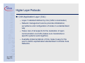
Higher Layer Protocols
CAN Application Layer (CAL)
– Layer-7-standard defined by CiA (CAN in Automation)
– Network management service provides initialization,
surveillance and configuration of nodes in a standardized
way
– Takes care of all aspects for the realization of open
communication via CAN (makes sure manufacturerspecific systems work together)
– Available implementations of CAL make it easy for the
user to define sophisticated standardized Controller Area
Networks
Dec 2000
Page 110
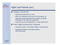
Higher Layer Protocols (cont.)
CANopen (CiA DS-301)
– Application profile based on CAL
– While CAL determines the way of communicating, an
Application Profile determines the meaning of specific
messages for the respective application
– Target: device interchangeability for certain applications
Further higher level protocols / standards:
– Automotive Sector: VOLCANO, OSEK (in development)
– Industrial Automation: DeviceNet (ODVA),
SDS (Honeywell)
Dec 2000
Page 111
Application Examples
CAN in motor vehicles (cars, trucks, buses)
– Enables communication between ECUs like engine
management system, anti-skid braking, gear control,
active suspension ... (power train)
– Used to control units like dashboard, lighting, air
conditioning, windows, central locking, airbag, seat belts
etc. (body control)
CAN in utility vehicles
– e.g. construction vehicles, forklifts, tractors etc.
– CAN used for power train and hydraulic control
Dec 2000
Page 112
Application Examples (cont.)
CAN in trains
– High need of data exchange between the different
electronic subsystem control units
– Mainly data about acceleration, braking, door control, error
messages etc. but also for diagnosis
CAN in industrial automation
– Excellent way of connecting all kinds of automation
equipment (control units, sensors and actuators)
– Used for initialization, program and parameter up/download, exchange of rated values / actual values,
diagnosis etc.
– Machine control (printing machines, paper- and textile
machines etc.): Connection of the different intelligent
subsystems
Dec 2000
Page 113
– Transport systems
Application Examples (cont.)
CAN in medical equipment
– Computer tomographs, X-ray machines, dentist chairs, wheel
chairs
CAN in building automation
– Heating, air conditioning, lighting, surveillance etc.
– Elevator and escalator control
CAN in household appliances
– Dishwashers, washing machines, even coffee machines...
CAN in office automation
– photo copier, interface to document handler, paper feeding
systems, sorter
– communicates status, allows in field connection or "hot swapping"
– DocuText Systems, i.e. automatic print, sort and bind on demand
Dec 2000
Page 114
Some things worth knowing about CAN
Developed in the mid-eighties by BOSCH
Asynchronous serial bus with linear bus structure and
equal nodes (Multi Master bus)
CAN does not address nodes (address information is
inside the messages combined with message priority)
Two bus states: dominant and recessive
Bus logic according to "Wired-AND" mechanism:
dominant bits (Zeros) override recessive bits (Ones)
Bus Access via CSMA/CD with NDA (Carrier Sense
Multiple Access/ Collision Detection with NonDestructive Arbitration)
Dec 2000
Page 115
Some things worth knowing about CAN (cont.)
recessive
NODE A
dominant
recessive
NODE B
dominant
bus idle
recessive
CAN BUS
dominant
Node B sends out recessive
but reads back dominant level
Dec 2000
Page 116
Node B loses arbitration
and switches to receive
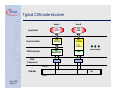
Typical CAN node structure
Node A
Node B
Application
e.g.
ABS
e.g.
EMS
Host-Controller
e.g.
80C166
e.g.
C167CR
or
C5x5Cx
CAN-Controller
e.g.
SAK82C900
CAN
(more nodes)
CANTransceiver
CAN_H
CAN-Bus
UDiff
CAN_L
Dec 2000
Page 117
CAN Data Frames
There are mainly two ways of communicating:
– One node is 'talking', all other nodes 'listen'
– Node A is asking Node B for something and gets the
answer.
To 'talk', CAN nodes use Data Frames.
– A Data Frame consists of an Identifier, the data to be
transmittedand a CRC-Checksum.
Identifier
Dec 2000
Page 118
Data Field (0..8 Bytes)
CRC-Field
CAN Data Frames (cont.)
– The identifier specifies the contents of the message
('engine speed', 'oil temperature', etc.) and the message
priority
– The Data Field contains the corresponding value
('6000 rpm', '110°C', etc.)
– The Cyclic Redundancy Check is used to detect
transmission errors.
– All nodes receive the Data Frame. Those who do not need
the information, just don't store it.
Dec 2000
Page 119
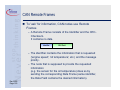
CAN Remote Frames
To 'ask' for information, CAN nodes use Remote
Frames.
– A Remote Frame consists of the Identifier and the CRCChecksum.
It contains no data.
Identifier
CRC-Field
– The identifier contains the information that is requested
('engine speed', 'oil temperature', etc.) and the message
priority.
– The node that is supposed to provide the requested
information
(e.g. the sensor for the oil temperature) does so by
sending the corresponding Data Frame (same identifier,
the Data Field contains the desired information).
Dec 2000
Page 120
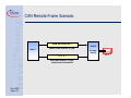
CAN Remote Frame Scenario
How hot is the oil ?
Node A
Remote Frame; Identifier 'oil_tmp'
115 °C !
Data Frame; Identifier 'oil_tmp';
contains desired information
Dec 2000
Page 121
Node B
(oil temp.sensor)
~~~~~
~~~~~
115°C
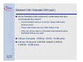
Standard CAN / Extended CAN
Most CAN nodes talk in the 'language' that most other
CAN nodes understand: They use Standard Data or
Remote Frames.
– A Standard Frame contains an identifier which is 11 bits
long.
– With this 11 bits, 211 (=2048) different messages can be
addressed.
– CAN nodes using Standard-CAN-Frames use the CAN
Specification Version 2.0A.
Some CAN nodes talk with a special 'accent':
They use Extended Data or Remote Frames.
– An Extended Frame contains an identifier which is 29 bits
long.
Dec 2000
Page 122
Standard CAN / Extended CAN (cont.)
– Over 536 million (229) different messages can be
addressed.
– CAN nodes using Extended-CAN-Frames use the CAN
Specification Version 2.0B (active).
Some Standard-CAN nodes don't understand this
'accent', but they tolerate it and just don't care.
– If an Extended Frame is 'on the air', these CAN nodes
cannot store the data, but they as well do not produce
errors.
– These CAN nodes use CAN Version 2.0A, but are also
known as Version 2.0B passive.
– They can be used in a Controller Area Network where
Extended Frames are used.
Dec 2000
Page 123
Standard CAN / Extended CAN (cont.)
Some Standard-CAN nodes don't understand and also
don't tolerate this 'accent'.
– If an Extended Frame is 'on the air', these CAN nodes
produce errors.
– These CAN nodes use only CAN Version 2.0A.
– They can not be used in a Controller Area Network where
Extended Frames are used.
Infineon 8 bit parts: C505CA, C515C: V2.0B active
Infineon 16 bit parts: C167CR, C164CI, C167CS,
C161CS: V2.0B active
Dec 2000
Page 124
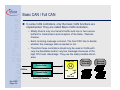
Basic CAN / Full CAN
In some CAN controllers, only the basic CAN functions are
implemented. They are called Basic-CAN controllers.
– Mostly there's only one transmit buffer and one or two receive
buffers for transmission and reception of the Data- / Remote
Frames.
– Each incoming message is stored. The host CPU has to decide
whether the message data is needed or not.
– Therefore these controllers should only be used in CANs with
very low baudrates and/or very few messages because of the
high CPU load. Advantage: They use the least possible silicon
area.
Host CPU
Receive Buffer
CAN Bus
Transmit Buffer
Basic-CAN Controller
Dec 2000
Page 125
low
high
CPU load
Messages
to be sent
Received
Messages
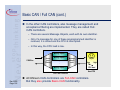
Basic CAN / Full CAN (cont.)
In the other CAN controllers, also message management and
acceptance filtering are implemented. They are called FullCAN controllers.
– There are several Message Objects, each with its own identifier.
– Only if a message for one of these preprogrammed identifier is
received, it is stored and the CPU is interrupted.
– In this way, the CPU load is low.
Message Object 1
CAN Bus
Acceptance
Filtering
Message Object 2
.
.
Message Object n
Full-CAN Controller
Dec 2000
Page 126
Message
Management
low
high
CPU load
Host CPU
All Infineon CAN-Controllers are Full-CAN controllers.
But they also provide Basic-CAN functionality.
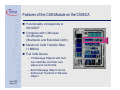
Features of the CAN Module on the C505CA
Functionality corresponds to
AN 82527
Complies with CAN spec
V2.0B active
(Standard- and Extended-CAN)
Maximum CAN Transfer Rate
(1 MBit/s)
Full CAN Device
– 15 Message Objects with their
own identifier and their own
status and control bits
– Each Message Object can be
defined as Transmit or Receive
Object
Dec 2000
Page 127
Features of the CAN Module on the C505CA
(cont.)
Programmable Mask Registers for Acceptance Filtering
– Global Mask for incoming Messages (Full-CAN-Objects)
– Additional Mask for Message Object 15
(Basic-CAN-Feature)
Basic CAN Feature (Message Object 15)
– Equipped with two Receive Buffers
– Own Mask Register for Acceptance Filtering
Connection to the Host CPU (C500-Core)
– Module access via SFRs in chip XRAM
– Interrupt connection to the CPU; Flexible interrupt event
control
To connect the application to CAN only a CAN
transceiver is needed
Dec 2000
Page 128
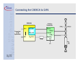
Connecting the C505CA to CAN
C505CA
P0.0
Connection
to the
Application
CAN-Bus
Transceiver
P4.5
CAN_RxD
Receive
CAN_H
P4.6
CAN_TxD
P3.7
Transmit
CAN_L
(Standby)
E.g. P1.0
R(opt)
Vref
n.c.
Dec 2000
Page 129
CAN_L
CAN_H
Exercise 5CAN_1 - Transmitting a Standard
CAN Message with the CAN Module
Objective:
– Generate a Standard CAN (11-bit-Identifier) Message with the
on-chip CAN Module*
– Use maximum bus speed of 1 Mbaud
– Use Message Object 5
– Use Identifier 0x123
– Use 8 Data Bytes containing the data 0x00, 0x11, …, 0x77.
* Hints:
– As long as no receiving node is connected to the KitCON-505C,
the C505CA will not receive an acknowledge for its transmission
and therefore will keep on trying to transmit the CAN message
“forever”.
– Connect another Starter Kit with CAN Capability or a CAN
Analyzer to the CAN bus to generate real CAN data transfers.
Dec 2000
Page 130
Exercise 5CAN_1 - DAvE Configurations
Start DAvE 2.1
Select “Create a new project” from the Startup Dialog or click
Select the microcontroller C505CA and click “Create”
(if this microcontroller is not on the list, you need to re-install it
from the DAvE 2.1 CD ROM*)
DAvE will create the project
Save your project by selecting “File | Save” or press
– Browse to directory “c:\hot505CA_1\5CAN_1\”
– Enter project name: “5CAN_1”
– Click “Save”
You will see the C505CA block diagram and the Project
Settings Window (configuration see next slide)
To get back to the Project Settings window in case you close
it: Select “File | Project Settings”
Dec 2000
Page 131
Exercise 5CAN_1 - DAvE Configurations (cont.)
Project Settings:
– System Clock:
External Oscillator Frequency: Set to 16 MHz (or the crystal
frequency of your KitCON-505C board)
CAN Baudrate
– Disable prescaler ( f [CAN] = f [OSC] / 2 )
Check this box only if the external oscillator frequency is less
than 16 MHz
– Close
Dec 2000
Page 132
Exercise 5CAN_1 - DAvE Configurations (cont.)
Configure CAN Module:
– Baudrate:
Bit Timing (in time quanta)
– Time Segment (TSeg1) before sample point [tq]: 4
– Time Segment (TSeg2) after sample point [tq]: 3
Baudrate: Enter desired Baudrate: 1000 Kbaud
– Objects:
Configure Object 5:
– Enable Control: Enable Message Object (MSGVAL)
– Identifier Selection: Standard 11 bit
– Message Direction: Transmit data frames, receive and answer remote
frames
– Data Length Code: Select 8 Data Bytes
– Data fields: Enter Data Bytes (0x00, 0x11, …, 0x77)
– Arbitration Register: Enter Identifier 11-bit: 0x123
– Save & close
– Functions: Include functions CAN_vInit and CAN_vTransmit
Dec 2000
Page 133
– Close
Exercise 5CAN_1 - DAvE Configurations (cont.)
Generate Code (
)
DAvE will show you all the files that he has generated
(File Viewer is opened automatically)
Dec 2000
Page 134
Exercise 5CAN_1 - µVision Configurations
Start Keil µVision2
NOTE:
µVision2 is able to read the DAvE project settings
(contained in the .dpt file) and automatically create a
µVision2 project. µVision2 will also automatically
generate the assembly startup file!
Create the new Project by opening the DAvE .dpt file
– Project: Open Project:
c:\hot505CA_1\5CAN_1\5CAN_1.dpt
Dec 2000
Page 135
Exercise 5CAN_1 - µVision Configurations (cont.)
Setup the µVision2 Target Options
– Project: Options for Target ‘Target 1’:
– Target:
Demo Tools always
place code at 0x4000
Use On-Chip XRAM (0xFC00-0xFFFF): Check
Off-chip Code Memory: Eprom Start - 0x4000
Eprom Size - 0x4000
Off-chip Xdata memory: no external RAM needed
– Debug:
Use: Keil Monitor-51 Driver - select
Load Application at Startup - check
– Click OK
Use the tree to open all .c files
Dec 2000
Page 136
Exercise 5CAN_1 - Add User Code
Edit MAIN.C:
– Transmit Message Object 5
– Include endless loop:
// USER CODE BEGIN (Main,2)
CAN_vTransmit(5);
while(1) {};
// USER CODE END
Build all
– This will compile and link the project and create an object
file and hex file.
Dec 2000
Page 137
Exercise 5CAN_1 - Run the Code
Make sure the evaluation board is powered and connected to
COM1
Connect the Oscilloscope to P4.0/TXDC (connector X3 pin
56)
Press the Reset Button on the board
Start the Debugger
Press “Run”
You should see signals similar to those on the next slide
To stop the code press the RESET button on the evaluation
board (the Halt button on the debugger will not work).
Dec 2000
Page 138
Exercise 5CAN_1 - Screenshot: CAN Message
V
10
8
6
4
2
0
-2
-4
-6
-8
-10
0
50
100
150
-8
-6
-4
200
250
300
350
P4.0 / TXDC (CAN TRANSMIT PIN)
The CAN message is automatically re-transmitted because no other
node is present to receive and acknowledge the message.
400
450
µs
500
6
8
µs
10
V
10
8
6
4
2
0
-2
-4
-6
-8
-10
-10
Dec 2000
Page 139
-2
0
2
P4.0 / TXDC (CAN TRANSMIT PIN)
2 usec/div
1 bit time = 1us -> 1Mb/s
4
Watchdog Timer
15-Bit timer overflow results in:
– Software reset
– Sets WDTS flag
Programmable input clock
High 7-bits reload register
Timer period from 153.6µs to 314.6ms @20 MHz
Can be reloaded with a special instruction sequence
– Set Bit WDT
– Set Bit SWDT
Dec 2000
Page 140
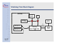
Watchdog Timer Block Diagram
WDTPSEL
7-bit
reload
zero
service
WDT & SWDT
CPU CLK / 2
CPU CLK / 16
Dec 2000
Page 141
WDTS
15-bit Timer
high 7 bits
low Byte
on
overflow
(7FFCH)
Software
Reset