1
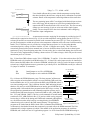
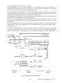
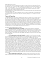
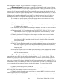
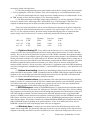
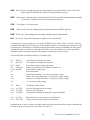
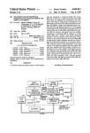
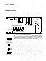
UTILITY BOARD
This chapter has been updated to describe circuit board Revision 3B, dated 3/30/93, and the current revision of
the DSP software 2.30.
Hardware Preparation
Fig. 4-1 shows the placement of the major components of the utility board. The board contains a DSP,
provision for up to 32k x 24 bit external program memory, regulators for +/- 12 volt power, two high current
drivers for heaters, four digital-to-analog converters (DACs), an analog-to-digital (A/D) converter with a
16-input multiplexer, 16 digital inputs and 16 digital outputs, three configurable analog input amplifiers, a
Analog Input Jumpers
Serial I/O
Temp
Sensor
Analog Input
Resistors
A/D
DACs
Power Transistors Regulators
User Interface
Connector
-12V
D00D07
D08D15
D16D23
U13
U19
U20
Backplane
Connector
Watchdog
Jumper
U31 = PAL
JP9
JP10
ROM
JP11
Program ROMs
Jumpers
+12V
DSP
Reset Switch
Rev. 3B
Power Source Jumpers
U34 =
74F07
GND
Fig. 4-1 - Component layout of Utility board.
Analog Input Jumpers
1
3
2
J J J J J J
P P P P P P
1 2 3 4 5 6
ROM Configuration Jumpers
A14 Write Enable
JP9 JP10
Watchdog Timer Jumper
JP11
1
Disabled
3
Enabled
2
Power Source Jumpers
2 3 1 2 3 1
JP7
JP8
Fig. 4-2 Jumper blocks
manual reset switch, and two 96-pin DIN connectors. Jumper blocks are located in
four areas, and control the configuration of the analog input amplifiers, the program
ROM memory, the watchdog timer, and the source of the +/- 15 volt power for the
board. Fig. 4-2 gives a close-up and labeling of these jumper blocks.
The analog input jumpers allow the user to configure the connection between the
three analog inputs AIN5-7 and the op amps that are connected to the 16-channel
MUX that goes to the A/D converter. Inverting, non-inverting, and differential
inputs can be configured. The gain and offset ranges of the amplifiers can also be
customized with the gain resistors R5 and R7 (in the AIN5 stage) and the offset
resistors R8 and R9. AIN5 is set up to read a temperature sensing diode mounted
near a cooled CCD. AIN5 is connected to the user interface connector pin C32, and
is wired for a default non-inverting gain of x2. A typical diode will exhibit a voltage
drop that ranges from 0.4 to 1.0 volts from room temperature to CCD operating
temperatures of below -100 degrees C. With a gain of x2 the output of this stage will
range from 0.8 to 2.0 volts, which will be sampled by the A/D converter whose input
voltage range is -3 to +3 volts. The diode used for laboratory test gave a reading of
$A50 ADU (2640 decimal) at room T to $C60 ADU (3168 decimal) for a cooled
CCD at -127 degrees C. These ADUs are measured by the host computer examining
Y:12 with the RDM command. This gives a relation between ADUs and temperature
4-1
Utility board - Updated May 12, 1994
User Interface Connector J1
Constant current
Source
To op amp
and A/D
T(deg C) = 773 - 0.2841 x ADU.
Users should calibrate their systems with the temperature sensing diodes
then have installed in their dewars, using the above calibration as an initial
estimate. Details of the temperature control algorithm are discussed below.
A27
AIN5
C32
0 to -10V
AOUT0
C25
35 ohms minimum
The two remaining inputs AIN6-7 are shipped with identical input resistors
to the AIN5 stage, but the jumpers are wired for a grounded input so the
output to the MUX connected to the A/D is at zero volts. The user can easily
change to a non-inverting x2 gain or an inverter with a simple jumper
change. The user should refer to the circuit schematic when configuring
Heater
Resistor alternative input configurations.
Fig. 4-3 Connection for CCD temperature control
A constant current source supplying 50 microamps is provided on pin A27,
and should be connected as shown in Fig. 4-3 for use with temperature sensing diodes near the CCD. Two
resistors (R1 and R2) are connected in parallel to the constant current source FET Q1. These are trimmed to
provide 50 microamps to within one percent so the temperature calibration will be the same for different utility
boards. The CCD heater power is provided as a voltage that ranges from 0 to -10 volts rather than the
conventional positive voltage in order to load the +12 and -12 supplies more equally. The CCD can be
conveniently heated with a resistor mounted near it, but care should be taken to prevent the on-board power
transistors Q2 or Q3 from dissipating more than 1.6 watts so they don’t overheat and damage the circuit board.
This can be easily implemented by installing a heater resistor of 35 ohms or larger, which will provide a maximum heater power of 2.8 watts.
Rev. 2.10 and later DSP software require 32k x 8 EEPROMs. To run Rev. 2.10 or later software three 28C256
EEPROMs need to be installed in the ROM sockets U13, U19 and U20, and a jumper needs to be installed on
JP9 to connect the DSP address line A14 to the EEPROM, which for 8k x 8 devices can be left open so a pull-up
resistor keeps it high. Hardware memory protection is provided by JP10 - the EEPROMs can only be written to
if a jumper is installed. To summarize:
JP9
JP10
Install jumper to use 32k x 8 EEPROMs
Install jumper to write enable the EEPROMs
U13, U19 and U20
D00 - D23
BOOTROM P: overlays
$6200
BOOTROM X: mem
$6100
BOOTROM P: mem
$6000
Not used
$4000
Fig. 4-4 shows the EEPROM memory map. The boot program "utilboot.asm"
starts execution at location $6000, which is accessed when the DSP reads from
location $E000 (since A15 is not wired from the DSP to the EEPROM) after it is
reset into operating mode 2. This is different from the VME and timing boards
that have only one byte-wide EEPROM and reset into the special DSP56001 boot APPL #2 P: mem $2300
APPL #1 Y: mem
$2180
operating mode 1 that reads the boot program into the DSP a byte at a time. The
APPL #1 X: mem
$2160
APPL #1 P: mem
boot program has communication and command recognition software and is
$2000
APPL #0 Y: mem
$1F00
loaded into the DSP internal memory locations P:$0000 to APL_ADR ($B0 for
APPL #0 X: mem
$1EE0
Rev. 2.25) and X:$0000 - $00FF. Code for several commands is located starting
at address P:OVL_ADR ($6200 for Rev. 2.25) and are called overlay programs
because they’re similar to the timing and VME board commands, although they APPLICATION #0
P: program memory
are a bit different on the utility board in executing directly from EEPROM
$00A0
Not used
$0000
without having to be written to the DSP internal memory. The application
Figure 4-4: EEPROM memory map.
program can be loaded into the DSP with the LDA # command from EEPROM,
or alternatively downloaded from the host computer by repeated calls to the WRM command. The LDA
command takes a single argument (#) which is the number of the application program to be read from
EEPROM, and is between 0 and 10. Application programs 1 to 10 are located in the EEPROM starting at
4-2
Utility board - Updated May 12, 1994
address $2000, and are allocated $300 words per program. They are read into the internal DSP memory spaces
P:APL_ADR to $1FF, X:COM_TBL to COM_TBL+15, and Y:0000 to Y:$00FF. The EEPROM memory map
is shown in Fig. 4-4, and the source code files "utilboot.asm" and "utilappl.asm" can be referred to for further
clarification. Currently an application program for testing the utility board is supplied, contained in the file
"utiltest.asm", and is assigned application number 1.
Application number zero is a special case and is designated for large application programs that cannot execute
in their entirety from internal DSP P: memory space. Instructions located at EEPROM address P:$200 up to
P:$1EE0) will be executed directly from EEPROM. Instructions from P:APL_ADR to P:$1FF will be read from
EEPROM into DSP P: memory by the ’LDA 0’ command. Its EEPROM memory map is also shown in Fig 4-4.
The PAL U31 has been designed into the current hardware revision 3B to generate DSP reset and interrupts
more reliably than earlier versions. The PAL has been programmed to reset the DSP to operating mode 2
wherein the DSP begins execution from EEPROM address $C000 after reset rather than reading the program
from byte-wide memory into DSP and then executing it, as is done in operating mode 1. Earlier revisions of the
DSP software than Rev. 2.25 can be executed on the current hardware revision 3B, but a different PAL will
need to be generated to reset the DSP to operating mode 1 instead.
The jumper JP11 is installed in the default configuration as shown in Fig. 4-2 to enable the watchdog timer. It
contains a timer circuit that will reset the DSP unless the watchdog timer is itself reset more often than that. The
intention is to require the DSP to reset the watchdog timer more often than every 10 milliseconds as a sign that
it is properly functioning; otherwise the DSP will be reset. The timer circuit is reset with a simple read instruction from location $FFF7.
The two jumpers JP7 and JP8 supply power to the board from either the backplane or the CCD/User connector.
The default is to supply +/- 15 volt power from the backplane to the utility board. Some users may desire to
supply it through the CCD/User connector instead so the utility board can independently verify the integrity of
the backplane power supply before turning it on and powering up the CCDs. In that case the two jumpers on
JP7-8 should be moved to the 2-3 position, the separate power should be run to the CCD/User connector
through pins C01 (+15 V) and A01 (-15 V), and a sample of the backplane power before it is supplied to the
backplane should be run to several of the inputs AIN8-15 after being suitably divided so they are in the range
of +3 to -3 volts that the A/D requires. Note that the spacing of the pins of JP7-8 are larger than 0.10 inches so
standard jumpers cannot be installed - the intention of having soldered wires is to discourage accidental
re-configurations.
The utility board needs to be installed in either slot 1 or slot 6 of the VME system backplane if a power control
board is being used. Alternatively, the daisy-chained lines A21, A22 and B04 need to have jumpers attached to
them on the VMEbus backplane to connect them between the utility board and the power control board.
Board Checkout
The following procedure is followed in verifying operation of the board. The commands to be executed are
described later in this chapter.
(1) Visually inspect board: The correct ROM(s) should be installed; if there is only one ROM it should be in
the left-most socket. Check the DSP. The jumpers described above should be installed correctly, as should all
the resistors.
(2) Power supplies: The +5 should be available at the logic devices, and +/- 12 volts should be available at the
regulators and the analog components. With the power control board installed, and the utility board installed in
either slot 1 or 6, PON will turn on the analog voltages. If it doesn’t install jumpers on the power control lines
4-3
Utility board - Updated May 12, 1994
to enable the power supplies. Spot check the voltages.
(3) Stand-alone DSP test: U31 pin 1 (PAL) should show a 1 millisecond period square wave after the LDA
command has been executed, low for 1/5 of its duty cycle. U8 pin 18 (the A/D) should have a low-going pulse
of 120 nanosec duration every one millisecond, the interrupt time.
(4) ROM boot: Monitor pin 20 on any of the ROMs. It should toggle for approx. 400 microsec after either the
reset button is depressed or digital power is turned on. After the 400 microsec it should stay in the high state,
and the DSP will begin normal operation. A storage scope is needed for this.
(5) Test Data Link: The data link to the timing board should be checked. Execute the DSP command TDL from
the host computer one million times. There should be no errors.
(6) Test DACs: Execute the DSP command TDA. Examine the outputs of the four DACs with a scope. They
should ramp linearly from about 0 to -9 volts with rounded bottoms (pins C24 and C25) and from -5 to +5 volts
(A24 and A25).
(7) Test A/D: Jumper pins A25 to C30. Execute the DSP command TAD. Monitor A24 and A25 with the scope.
A25 should show a ramp, and A24 should show a somewhat different ramp with a small discontinuity when
A25 crosses zero volts.
(8) Test MUX: With the DSP in a free-running, interrupt driven state (the board may need to be reset) examine
U8 pin 20 (the A/D) and U31 pin 1 (the PAL) with a scope, triggering on the latter. The former is the output of
the MUX, and should show 12 step changes as the various inputs are connected to the MUX. The envelope
Front connector
20 MHz clock
DUART
External
Reset
Counter
1 millisec clock
Port A
Watchdog
Reset
Timer
Asynchronous Serial Link (SCI)
IRQA
Port B
Port A
Status and control lines
Power, Board Temp
Port A
12-bit
DSP56001
A/D
12-bit
DAC
(4)
EEPROM
32k x 24
Address
Decoder
Address Bus
A00-A15
RXD, TXD
Select MUX
Read A/D
Read Digital
Write Digital
Write DAC (4)
R/W DUART
Data Bus
D00-D23
16 16-input
MUX
4
16-bit
Latch
16
16-bit
Driver
16
Front connector
5
11
Controller
Backplane
Fig. 4-5 Block diagram of the utility board.
4-4
Utility board - Updated May 12, 1994
pattern approximates a pyramid.
(9) Test A/D inputs: Connect an adjustable power supply to several AIN pins in turn and examine U8 pin 20
(the A/D) with a scope. As the power supply is adjusted one of the positions in the ramp will change too. Vary
AIN5 = C32 over the range of -1.5 to +1.5 volts, while the MUX should vary over -3 to +3 volts. Do this for
AIN6,7 as well if desired, after rejumpering the inputs. Inputs AIN8-15 should be connected to a variable
voltage source as the A/D input is examined for unity gain.
(10) Board temperature: Cool the temperature sensor U5 a little with a localizeable coolant, and watch the first
ramp position change a little.
(11) Constant current source: Pin A27 should have close to 12 volts on it with no load. 50 microamps should
flow through it when connected to a load. This can be checked by looking for a 1.0 volt drop accross a 20k
resistor.
Theory of Operation
The utility board provides a miscellany of support functions that are not directly involved with the readout of
the CCDs. These include exposure timing, CCD temperature control, and system voltage and temperature
monitoring. Based around a Motorola DSP56001 microprocessor, the utility board can be programmed by the
user to support other functions such as an additional temperature controller, dewar level and ID, shutter status,
LED drivers for status indication, and switch monitoring for direct system control without a host computer . A
interrupt circuit forces the DSP to update all inputs and outputs every millisecond, providing precise exposure
timing, while 12-bit A/D and D/A converters offer good analog precision. Commands are received from the
timing board over a fast serial link and processed as necessary. Additional serial links can be used to communicate with other devices. A block diagram of the board is shown in Fig. 4-5.
The following utility board functions are available:
(1) Command and Interrupt processing: The boot routine "utilboot.asm" loaded from
EEPROM to internal DSP memory soon after DSP reset provides communications service through the serial
link to the backplane, services external commands. It follows the protocol discussed in the systems manual of
processing and generating header ID words that contain three bytes - source byte, a destination byte and a
number of words byte. The commands TDL, RDM, WRM, LDA and RST are implemented in the same fashion
on all the DSP boards.
(2) CCD temperature monitor and control: An amplifier circuit U1b measures the voltage
drop on a temperature sensing diode located near the CCD. The amplifier output is connected to one of the 16
inputs (#5) of a multiplexer that is connected to a 12-bit A/D converter. The digital count is inversely
proportional to temperature. A target temperature is entered at location Y:$1C=28, and the difference between
it and the actual temperature located at Y:$0C=12 is multiplied by a constant located at Y:$1D=29 to add to the
current value of the heater voltage. To start up the temperature controller a reasonable value is written to the
target temperature location Y:$1C=28, as the default value of $FFF will disable the heater. The temperature
controller can be disabled by writing a value of $FFF to the desired temperature location, since the heater will
quickly be turned off since the target temperature is so much lower than the actual temperature. The default
value of the proportionality constant is $010000, which is appropriate to our laboratory test system that tightly
couples the dewar cooling to the CCD. This will probably need to be tuned by users to reflect the thermal time
constant of their cooling systems, with values as small as $001000 being appropriate for slower, more thermally
efficient systems. The heater voltage time history should be monitored at the user interface connector pin C25
or by monitoring the digital counts at Y:2 written to the heater DAC0 to determine if it is behaving properly. If
the heater voltage oscillates from zero to maximum heat without damping itself out after a few minutes then the
constant will have to be made smaller. Similarly, if the heater seems to take a long time to settle to the correct
value as it oscillates by a small amount from its average, then it can be sped up by entering a larger proportionality constant.
(3) Board temperature monitoring: A temperature monitor is placed directly on the utility
board, and connected to one of the sixteen inputs to the multiplexer, allowing the host computer to read the
4-5
Utility board - Updated May 12, 1994
board temperature at any time. The gain calibration is 0.38 degrees C per ADU.
(4) Exposure timing: Exposure timing is controlled by counting millisecond interrupts. It begins
counting from zero at the start of an exposure up to a target exposure time. Counting can be paused at any time,
while the exposure time can be changed by setting a different exposure time, which if less than the elapsed
exposure time will cause an immediate readout. Upon reaching the target exposure time the utility board will
close the shutter if needed and signal to the timing board via a serial line that readout should begin. The target
exposure and elapsed times are readable by the host computer at any time and their addresses are listed below.
The shutter can be controlled with the utility board, with bit 0 of the software control word at X:1 being set
indicating that the shutter is to be opened at the beginning of the exposure and closed when it terminates.
The command SEX starts an exposure, initiates the exposure timer and starts readout. It is a fairly
integrated command that is defined in the "utilappl.asm" file as follows:
(1) Utility board receives and recognizes SEX command.
(2) Utility board issues ’CLR’ command to timing board to clear the CCD, and waits for it to reply with
a ’DON when this is complete.
(3) If X:OPTIONS=1 bit OPT_SH=0 equals 1 then open the shutter. The shutter can either be connected to the utility board (preferred) or the timing board (older systems).
(4) The elaspsed time at Y:23 is zeroed, and the status bit X:STATUST_EX bit OPT_EX=1 is set to
indicate that an exposure is in progress so the elapsed time will be incremented by 1 each
millisecond interrupt.
(5) The utility board sends a DON reply to the host computer to indicate that the exposure has been
started.
(6) Once the elapsed time equals the target time readout is initiated by the utility board. The shutter is
closed if needed. A RDC command is issued by the utility board to both the timing and the
VME interface boards.
(7) The timing board begins readout and transfers pixel data to the VME interface board.
(8) The VME interface board interprets all data coming from the timing board as pixel data and places
them in the image areas specified until the specified number of pixels have been transferred,
after which it issues a DON command to the host computer and switches to normal command
interpreting mode.
Note that the host computer receives two DON replies after issuing the SEX command - one from the
utility board soon after the command is issued and the second from the VME interface board
when the readout has completed.
(5) Power Supply monitoring and control: Four of the inputs to the 16-input multiplexer are
connected to the power supply lines that are bussed on the backplane: +5, +15, -15 and +36 volts. They are
sampled every millisecond and placed in a table in DSP memory which can be accessed anytime by the host
computer with a ’RDM’ command. Additionally, a power-up routine successively turns on each analog power
supply with a digital on/off line from the backplane after the timing board has successfully loaded all its DACs.
This function has been developed and is part of Rev. 2.25 software, and is to be used in systems equipped with
a power control board. Power turn-on is initiated with the PON command. The sequence is as follows:
(1) The utility board boots up from on-board ROM.
(2) The host computer should issue a LDA to the timing board, and LDA and PON commands to the
utility board. PON is the command to start the power on sequence.
(3) The utility board will reset the power control board by asserting PWRST to initialize its on board
counters and turn off the power supply switches.
(4) The utility board issues an IDLE command to the timing board to ensure that its clock driver DACs
4-6
Utility board - Updated May 12, 1994
are properly loaded with legal values.
(5) The utility board instructs the power control board to turn on the low voltage power lines (nominally
+/- 15V) by toggling the LVEN line 128 times. These will be ramped up over a 20 millisecond time period.
(6) The utility board samples the low voltage power lines, making sure they are within tolerance. If not,
an ’ERR’ message is sent to the host computer. If yes, processing continues.
(7) The utility board turns on the high voltage supply (nominally +36 volts) by toggling the HVEN line
128 times. It checks it to be within range after 5 milliseconds. If yes, a DON message is sent to the host
computer to indicate that power has been succesfully turned on. Otherwise an ERR message is sent.
If the power control board fails to turn on successfully the host computer can be used to examine the
voltages seen by the utility board during the power on sequence. The target voltages +HV (+36), +LV (+15)
and -LV (-15), the required tolerances, the actual voltage measured during the power on sequence and the
current voltage values are all stored in Y: memory on the utility board in the following locations:
+HV (+36)
+LV (+15)
-LV (-15)
Target
Y:$1F
Y:$21
Y:$23
Tolerance
Y:$20
Y:$22
Y:$24
Power on
Y:$25
Y:$26
Y:$27
Current
Y:$8
Y:$9
Y:$A
(6) Digital and Analog I/O: Every millisecond an interrupt service is entered that reads the
voltages at each of the sixteen digital inputs and sixteen analog inputs, and stores them in a table in the DSP
memory. They can be read at any time by the host processor with a ’RDM’ command to the appropriate address
given below. A table of sixteen digital outputs, plus shutter, and four analog outputs is also maintained in DSP
memory and written to latches every millisecond as well. Whenever the host computer needs to change any of
these values it writes new values into the correct DSP memory location with the ’WRM’ command, after which
the DSP will update the latches on the next interrupt cycle, after a delay of at most one millisecond. The
analog-to-digital converter is 12-bits in accuracy, and presents 2’s complement codes to the DSP program that
converts it to straight binary with $0000 representing -3 volts and $0FFF representing +3 volts input to the A/D
converter.
(7) Software downloading: Capability for downloading software from the host computer to the
utility board DSP is done with the ’WRM’ command provided on all DSPs. DSP software compiled on the host
computer is sent over the fiber optic link to the timing board, which relays it to the DSP on the utility board.
There it is written to the DSP internal memory for direct execution.
(8) Serial communications: An asynchronous serial connection between the utility and timing
boards is provided. It is connected to the SCI (Serial Communications Interface) port of both DSPs, operates at
312.5 kbits/second, and is serviced by interrupt service routines at each end. It is the only communications
channel between the utility board and the timing and VME interface boards.
(9) EEPROM support: A bank of fast EEPROM memory is supplied with each board that contains
the boot code in compiled from the source file "utilboot.asm". This bank is fairly large (32k x 24 bits), enabling
large programs to be executed by the utility board, and timing board programs to be downloaded over the serial
link connecting the two boards. The time critical portion of the DSP program operates out of internal DSP
memory at 10 MIPS, whereas non-time critical portions operates more slowly out of the EEPROM, because the
DSP requires extra clock cycles for an external memory access. EEPROM programming support is described
in the software chapter. The memory read and write commands RDM and WRM operate transparently on either
DSP or EEPROM memory depending on the specified address. A time of 10 milliseconds for any write to
EEPROM is required for each word, and page mode writes are not supported.
(10) Watchdog timer: It monitors the execution of the on-board DSP processor and one of the
outputs of the timing board. If it detects that either board is not alive, an error message will be sent to the host
computer. If the utility board DSP is not alive the DSP will be reset, whereas the timing board will be reset or
4-7
Utility board - Updated May 12, 1994
not depending on the setting of a control bit. Resetting the DSP will cause the current exposure to be lost, and
corrective action must be taken by the host computer.
(11) Board Reset: A reset circuit on the board is implemented with the PAL (programmable array
logic) chip U31 to reset the DSP and generate interrupts to it from a variety of signal sources. The PAL equation
is as follows:
RESETI = (QRES # UTLRST’ # UTLRSW’)’
IRQA = RESETI & MSCK
IRQB = RESETI’ # (PULSE7 & IIRQB)
where # means logical OR, & means logical AND and ’ means logical invert. The DSP reset line RESETI will
go low (is asserted) when either the watchdog timer line QRES goes high, the power control board brings the
UTLRST line low from the system backplane, the on-board reset switch is depressed or the EXRESW pin on
the user connector is grounded, the later two causing UTLRSW to go low. The DSP interrupt line IRQA goes
low if the DSP reset line RESETI is asserted or if the millisecond interrupt line MSCK goes low. The IRQA line
is sampled along with IRQB when RESETI is asserted to determine the operating mode of the DSP, which
determines its internal memory configuration. IRQB goes high if the DSP reset line goes low, so the DSP is
placed in operating mode 2 on reset, which starts the DSP executing code read starting at external memory
address $E000, which is mapped to the EEPROMs. IRQB is asserted as an interrupt when either PULSE7 or
IIRQB goes low; PULSE7 is generated by the timing board, allowing it to interrupt the utility board at will, and
the IIRQB is bussed along the backplane allowing external devices to interrupt the utility board as well. As of
Rev. 2.25 neither of these interrupt sources are connected to anything and interrupt service routine is not written
to support IRQB, so it exists for future system enhancements.
(12) System Reset: An optically isolated line is provided on the front-plane connector that can be
used to reset the utility board from a remote location in the event of a catastrophic failure.
(13) Additional serial communications: Two additional bidirectional asynchronous serial
ports are provided. One is optically isolated and wired to the front-plane connector for use with terminals or
external computer systems, and may be particularly useful for debugging. The second one is connected to the
backplane for communicating with other devices that may be installed by the user on the backplane. These are
provided by the serial controller U25, which is not currently being populated on distributed utility boards, nor
is it supported by DSP software. Users desiring this support should contact us.
Software Commands
The DSP software chapter details the commands that are located in the "utilboot.asm" program that is loaded
from EEPROM soon after the DSP is reset, and are in common with the other DSP boards in the system. The
file "utilappl.asm" contains the main exposure control, power on, interrupt servicing and temperature control
software. It is the designated application number 0 that can be executed directly from EEPROM, and is loaded
with the ’LDA 0" command. It interprets the following commands:
SEX - "Start exposure". Immediately begin a timed exposure by issuing a CLR command to the timing board,
waiting for it to terminate, opening the shutter if the shutter status bit is set, beginning the timer
countdown according to the exposure time word stored in Y: data memory, and issuing
commands to the timing and VME interface board to begin readout.
PEX - "Pause exposure". Simply close the shutter , stop the timer and wait until a REX command is issued.
REX - "Resume exposure". Open the shutter if needed and resume the normal exposure sequence.
4-8
Utility board - Updated May 12, 1994
AEX - "Abort exposure". Immediately stop exposing altogether by closing the shutter, put the CCD in idle
mode, and put the VME interface board in command interpreting mode.
OSH - "Open shutter". Open the shutter. Normally this will be done by the SEX command, but this command
is provided as a manual override for testing and special purposes.
CSH - "Close shutter". Close the shutter.
SYR - "System reset". Reset the timing board by pulling the backplane SYSRST signal low.
PON - "Power on". Turn analog power on safely, using the power control board.
POF - "Power Off". Turn off the analog power using the power control board.
Commands may be sent in groups to be executed by the DSP as it gets to them. There is a circular buffer for
commands in the DSP that is 32 words long, so fairly lengthy sequences of commands may be sent at once. The
exception to this is that during CCD readout the timing board cannot send any commands to the utility board.
Commands already received by the command buffer will be executed normally. None of these application
commands requires an argument and all of them generate a DON reply after they execute.
The following table is maintained starting in Y: memory space:
Y:0
Y:1
Y:2-5
Y:6
Y:7-22
Y:7
Y:8
Y:9
Y:10
Y:11
DIG_IN
DIG_OUT
DAC#
NUM_AD
AD_IN#
16-bit digital word input to the board
16-bit digital word output from the board
Four analog voltages output by the board
Number of A/D inputs to be monitored. Default is 16
Sixteen analog voltages input
Board temperature
High voltage (nominally +36 volts) power supply voltage
Positive low voltage (nominally +15 volts) power supply voltage
Negative low voltage (nominally -15 volts) power supply voltage
+5 volts power supply voltage
Y:2
Y:12
Y:28
Y:29
DAC0
A_CCDT
T_CCDT
T_COEFF
CCD Heater voltage output
Actual CCD temperature diode voltage
Desired CCD temperature
Proportionality constant for temperature control algorithmn
Y:23
Y:24
EL_TIM
TGT_TIM
Elapsed time since start of exposure in milliseconds
Target, or desired, exposure time in milliseconds
In addition there are two X: memory words that control and monitor board and software status. Additional bits
are defined, but are of interest only to the software, not the user.
4-9
Utility board - Updated May 12, 1994
X:0
Bit 0
Bit 1
Bit 2
STATUS
ADC
Timer
Shutter
Board status word
Set it A/Ds and temperature control needs updating
Set if a timed exposure is in progress
Set if shutter is open
X:1
Bit 0
SOFTWARE CONTROL
Shutter
Set if shutter is to be opened when exposure starts.
Other bit assignments will be added as we go along following this general structure. All these words are
serviced every one millisecond, as signalled by the external interrupt generation circuitry.
The file "utiltest.asm" is assigned application number 1, and contains several simple routines written to test the
functionality of the utility board. These commands should NOT be executed with the utility board user connector plugged into a CCD system. The section above describing the board checkout procedure should be referred
to for further details concerning system interconnection when executing these commands.
TDA - "Test Digital-to-Analog converters". This will generate ramping numbers that are written to the four
DACs so their outputs can be examined with an oscilloscope.
TAD - "Test Analog-to-Digital converter". This will generate a ramp for a DAC that is wired by the user to
one of the analog MUX inputs for conversion by the A/D converter. Its digitized output is then
written to a second DAC whose analog output is examined by a scope and compared to the first
DAC’s output.
TDG - "Test Digital". Test the digital input and output circuits by reading the 16 inputs and outputting them
to each digital output in turn, right shifting the 16 bit data word.
The CCD/User connector is a 96-pin female connector mounted near the reset switch. Its pinout is given below,
which the pinout for the system backplane connector is given in the system chapter above.
Software revision history
Several changes were made to the following files in the transition from Rev. 2.25 to 2.30:
utilboot.asm - The SCI receiver ISR was compressed considerably. It is the same ISR as timboot.asm,
except register R2 points to the SCI address, not R0.
utilappl.asm (1) The OSHUT and CSHUT routines no longer send messages to the timing board to open or
close the shutter. We now assume that the shutter is connected to this board.
(2) The interrupt structure was changes considerably to minimize the code in interrupt service
routines so registers and stacks are not altered while processing an interrupt. Specifically, the TIMER
ISR only counts down the timer and closes the shutter, setting the ST_READ bit it readout is to occur,
which is now in a program routine, with the bit checked at the START location. The SERVICE
soubroutine was introduced to service the millisecond interrupts, and does all the A/D, DAC, digital
4-10
Utility board - Updated May 12, 1994
I/O and temperature control servicing.
(3) A new STATUS bit ST_READ was introduced to indicate that readout is to be initiated
when the timer counts to zero. This is to handle situations when the timer counts and readout is not to
occur, and to separate the readout functions from the timer ISR servicing.
(4) Introduce power OFF command = POF. It simply resets the power control board.
Pinout - CCD/User conector
Pin #
1
2
3
4
5
6
7
8
9
10
11
12
13
14
15
16
17
18
19
20
21
22
23
24
25
26
27
28
29
30
31
32
VSB
ROW a
VSBDOUT7
DOUT6
DOUT5
DOUT4
DOUT3
DOUT2
DOUT1
DOUT0
DOUT15
DOUT14
DOUT13
DOUT12
DOUT11
DOUT10
DOUT9
DOUT8
GND
SEROUTSEROUT+
NC
EXRESW
GND
AOUT3
AOUT2
GND
CONST-CURR
AIN14
AIN12
AIN10
AIN8
AIN6
ROW b
GND
GND
GND
GND
GND
GND
GND
GND
GND
GND
GND
GND
GND
GND
GND
GND
GND
GND
GND
GND
GND
GND
GND
GND
GND
GND
GND
GND
GND
N/C
N/C
N/C
ROW c
VSB+
DIN7
DIN6
DIN5
DIN4
DIN3
DIN2
DIN1
DIN0
DIN15
DIN14
DIN13
DIN12
DIN11
DIN10
DIN9
DIN8
GND
SERINSERIN+
NC
SHUTTER
GND
AOUT1
AOUT0
GND
AIN15
AIN13
AIN11
AIN9
AIN7
AIN5
+/- 15 volts power supply pins from form CCD/User connector as an alternative to the
backplane connector. JP7 and JP8 need to be set properly to utilize it.
4-11
Utility board - Updated May 12, 1994
AIN
AOUT
DIN
DOUT
SERIN
SEROUT
EXRES W
SHUTTER
CONST-CURR
Analog inputs, 5-15. The input range of 5-7 is described on page 4-1, and the
remaining ones all have an input range of -3 to +3 volts.
Analog output 0-4. AIN0-1 are high current, unipolar outputs for driving heaters from
0 to -10 volts, while AIN2-3 are low current, bipolar outputs of -5 to +5 volts.
Digital inputs from 0 to 15. These are read every millisecond and stored in the DSP
data memory space. They have resistors to pull them high if not connected.
Digital outputs from 0 to 15. These are written from DSP data memory every
millisecond. They are pulled up so they will be high until set by the DSP.
Two pins, + and -, for an asynchronous serial link generated by a 2681 chip. The two
inputs are optically isolated from the board.
Two pins, + and -, for an asynchronous serial link generated by a 2681 chip.
An input signal that will reset the DSP if brought low.
An open-collector output signal generated by this board. Low means open shutter.
A constant current source for CCD temperature control. See Fig. 4-3.
4-12
Utility board - Updated May 12, 1994