1
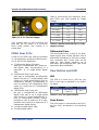
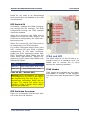
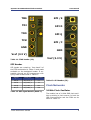
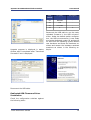
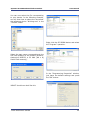
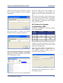
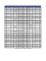
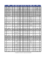
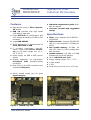
Spartan-3E FPGA
Industrial Micromodule
Trenz Electronic GmbH
[email protected]
www.trenz-electronic.de
Rev 1.19 as of 2011-10-04
User Manual
Features
■ Industrial temperature grade available on request
■ Low-cost, versatile and ruggedized
design
■ High-density plug-in Xilinx Spartan3E module
■ USB 2.0 interface with high speed
(480 Mbit/s) data rate
■ Large SPI flash for configuration and
user storage accessible via USB or SPI
connector
■ Large DDR-SDRAM
■ FPGA configuration is implemented via
JTAG, SPI Flash or USB
■ 3 on-board high-power, high-efficiency, switch-mode DC-DC converters (1 A for each voltage rail: 1.2 V,
2.5 V, 3.3 V)
■ Power supply via USB or B2B (carrier
board)
■ Flexible expansion via high-density
shockproof B2B (board-to-board)
connectors
■ Most I/O's on the B2B connectors are
routed as LVDS pairs
Specifications
■ FPGA: Xilinx Spartan-3E XC3S500E –
XC3S1600E
■ USB controller: Cypress EZ-USB FX2
USB 2.0 microcontroller CY7C68013A56LFX
■ Non volatile memory: 16 MBit - 64
Mbit SPI Flash for FPGA-configuration
and user data
■ Volatile memory: 512 Mbit x 16 DDR
SDRAM with up to 666 Mbyte/s
■ Up to 110 FPGA user I/Os
■ Supply voltage range: 4.0 V – 5.5 V
■ 1 push-button
■ 1 LED
■ Small size (only 40.5 mm x 47.5 mm)
■ Evenly spread supply pins for good
signal integrity
Figure 2: TE0300: top view.
Trenz Electronic GmbH
Figure 1: TE0300: bottom view.
1
Table of Contents
Features........................................................................................................................1
Specifications................................................................................................................1
Applications...................................................................................................................3
Description....................................................................................................................3
Physical Features...........................................................................................................3
Power Supply.................................................................................................................5
FPGA User I/Os..............................................................................................................6
User Button and LED.......................................................................................................7
Configuration Switches...................................................................................................7
JTAG and SPI.................................................................................................................8
Clock Networks..............................................................................................................9
On-board Memories......................................................................................................10
Module Configuration....................................................................................................11
Changes from TE0300-00 to TE0300-01..........................................................................24
Ordering Information....................................................................................................24
Revision History...........................................................................................................24
Legal Notices...............................................................................................................25
Environmental protection...............................................................................................26
Appendix.....................................................................................................................27
Spartan-3E FPGA Industrial Micromodule
User Manual
Applications
■
■
■
■
■
■
■
IP (intellectual property) development
Digital signal processing
Image processing
Cryptography
Industrial control
Low-power design
General-purpose prototyping platform
Description
The FPGA industrial micromodule integrates a leading edge Xilinx Spartan-3E
FPGA, an USB 2.0 microcontroller, configuration Flash, DDR SDRAM and power supplies on a tiny footprint. A large number of
configurable I/Os are provided via B2B
mini-connectors.
The module is intended to be used as an
OEM board, or to be combined with our
carrier boards. It is a powerful system
widely used for educational and research
activities.
Figure 4: connector receptacles J4
and J5 (bottom view).
Figure 3: module dimensions in mm
(top view).
The module has two B2B (board-to-board)
receptacle connectors (J4 and J5) for a
total of 160 contacts (Figure 5).
Boards with other configurations, larger
FPGA's or equipped with industrial temperature grade parts are available on request.
Software for SPI flash programming over
USB as well as reference designs for high
speed data transfer over USB are included.
Physical Features
Board Dimensions
The module measures 40.50 mm by 47.50
mm.
Figure 5: micromodule receptacle.
The ordering numbers of the connector receptacles are given in Table 1.
Board-to-Board Connectors
Trenz Electronic GmbH
3
Spartan-3E FPGA Industrial Micromodule
supplier
header
Digikey
H11113CT-ND
H11113TR-ND
H11113DKR-ND
Hirose
DF17(3.0)-80DS-0.5V(57)
Trenz Electronic
22684
Table 1: equivalent part numbers of
the receptacle connectors J4 and J5.
The on-board receptacles mate with their
corresponding headers on the carrier board
(Figure 6).
User Manual
Figure 7: stacking height (h).
The stacking height of the TE0300 B2B
connectors is 7 (seven) mm. The stacking
height does not include the solder paste
thickness.
USB Connector
The micromodule uses a mini-USB (B type)
receptacle connector.
Figure 6: mating header.
The ordering number of the headers is given in Table 2.
supplier
header
Digikey
H11148DKR-ND
H11148TR-ND
H11148CT-ND
Hirose
DF17(4.0)-80DP-0.5V(57)
Trenz Electronic
22938
Table 2: equivalent part numbers of
the mating connectors.
Figure 7 shows the definition of stacking
height featured by the combination of the
TE0300 receptacle with its corresponding
header.
Trenz Electronic GmbH
Figure 8: mini-USB (B type) receptacle
connector.
Power Supply
The module can be powered by the B2B
connector or the USB connector. If both
power supplies are available, the B2B connector power supply takes precedence,
disabling the USB power supply automatically.
B2B Connector Power Supply
The B2B connector power supply requires
a single nominal 5 V DC power supply. The
power is usually supplied to the module
through the 5 V contacts (5Vb2b) of the
B2B connectors J5 (see Appendix). The recommended minimum supply voltage is
4
Spartan-3E FPGA Industrial Micromodule
4 V. The maximum supply voltage is 5.5 V.
The recommended maximum continuous
supply current is 1.5 A.
USB Power Supply
The module is powered by the USB connector if the following conditions are met:
■ the module is equipped with an USB
connector,
■ the module is connected to a USB bus,
■ no power supply is provided by the B2B
connectors.
In this case, other components (e.g. extension or carrier boards) may also be
powered by the corresponding 5 Volt line
(5V) of the B2B connector J5.
On-board Power Rails
Three on-board voltage regulators provide
the following power supply rails needed by
the components on the micromodule:
■ 1.2 V, 1 A max
■ 2.5 V, 1 A max
■ 3.3 V, 1 A max
The power rails are available for the FPGA
and can be shared with a baseboard by the
corresponding lines of the B2B connectors J4 and J5. Please note that the power
consumption of the FPGA is highly dependent on the design actually loaded.
So please use a tool like Xilinx Xpower to
determine the expected power consumption.
Even if the provided voltages of the module are not used on the baseboard, it is recommended to bypass them to ground
with 10 nF - 100 nF capacitors.
User Manual
Bank
Supply
Voltage (V)
Min
(V)
Max
(V)
B0
VccIO
1.2
3.3
B1
2,5
-
-
B2
3,3
-
-
B3
3,3
-
-
Table 3: I/O banks power supply.
Voltage for banks B1, B2 and B3 is fixed
respectively to 2,5 V, 3,3 V and 3,3 V.
Voltage VccIO for bank B0 shall span from
1.2 V to 3.3 V. VccIO can be supplied
either externally or internally to the micromodule.
Warning! Spartan-3 I/Os are not 5 V tolerant. Applying more than the recommended operating voltages at any pin, results
in a damaged FPGA (see Xilinx Answer
AR#19146).
Externally Supplied VccIO
VccIO can be externally supplied over the
B2B connector J4. If bank B0 is not used,
then VccIO can be left open.
Internally Supplied VccIO
If VccIO is not externally supplied, it can
be internally supplied by one of the internal power rails of 2.5 V and 3.3 V. This is
possible by short-circuiting one of the two
pad pairs placed on the right of connector
J4 at the top right corner of the bottom
side of the micromodule.
Figure 9 shows how to short-circuit VccIO
to internal 3.3 V power rail.
Figure 10 shows how to short-circuit VccIO
to internal 2.5 V power rail.
I/O Banks Power Supply
The Spartan-3E architecture organizes
I/Os into four I/O banks (see Table 3).
Trenz Electronic GmbH
5
Spartan-3E FPGA Industrial Micromodule
User Manual
Table 4 summarizes the maximum available FPGA user I/Os divided by supply
voltage.
Figure 9:
10:R102
R103pad
padpair
pair(blue
(bluehighhighlight) for 3.3
2.5 V internal supply.
Two suitable ways of shirt-circuiting the
paid pair are by means of a zero-ohm
0603 (1608 metric) chip resistor or a
solder blob.
type
VccIO
3.3 V
diff. I/O pairs
≤ 18
≤ 23
diff inputs
≤1
none
diff. clocks
≤4
≤1
s. e. I/Os
≤ 46
≤ 58
s. e. inputs
≤2
≤4
s. e. clocks
≤8
≤3
Table 4: maximum FPGA user I/Os by
supply voltage.
Differential Pairs
FPGA User I/Os
A total of 110 FPGA user I/Os are available
on corresponding contacts of B2B connectors J4 and J5 (see Appendix).
■ 37 differential digital I/O pairs:
each pair is configurable as 2 single-ended digital I/Os, corresponding to a
maximum of 74 single-ended digital
I/Os;
■ 4 differential clock input pairs:
each pair is configurable as differential
digital I/O pair or 2 single-ended clock
inputs or 2 single-ended digital I/Os (or
combination thereof), corresponding to
from a maximum of 8 independent clock
inputs to a maximum of 8 independent
digital I/Os;
■ 1 differential clock input pair:
the pair is configurable as differential
digital input pair or as 2 single-ended
clock inputs or 2 single-ended digital inputs (or combination thereof), corresponding to from a maximum of 2 independent clock inputs to a maximum of 2
independent digital inputs;
■ 21 single-ended digital I/Os;
■ 5 single-ended inputs.
Trenz Electronic GmbH
The micromodule has a total of 42 differential signal pairs routed pairwise with a
differential impedance of 100 ohm to adjacent connector pins. These lines can be
used for high speed signaling up to
666 Mbit/s per differential pair (see Xilinx
Application Note XAPP485).
User Button and LED
LED
The LED is lit when the U_LED line (pin
R10) is set high as detailed in the following table.
Signal
FPGA pin
FPGA ball
U_LED
IO_L15P_2
(bank 2)
R10
Table 5: user led signal details.
Push Button
The push button is connected to the PB input (pin V16). as detailed in the following
table.
6
Spartan-3E FPGA Industrial Micromodule
Signal
FPGA pin
FPGA ball
PB
IP
(bank 2)
V16
Table 6: user button signal details.
The input is normally low. The input is
pulled up when pressed.
Configuration Switches
The micromodule hosts 4 DIP switches on
the top side: S1; S2, S3 and S4.
For customers requesting a sufficient
amount of units, the micromodules can be
manufactured replacing the switches by
fixed connections.
DIP Switch S1
S1 enables / disables the communication
between the Cypress EZ-USB FX2 microcontroller and the I2C CMOS Serial EEPROM.
Turn S1 off when programming the USB
EEPROM (storing the USB vendor ID and
device ID). This will force the USB microcontroller to provide its default vendor ID
and device ID.
S1
position
EEPROM (on)*
EEPROM enabled
Off (off)
EEPROM disabled
Table 7: S1 (* default: EEPROM).
For further information, please read paragraph “Software Configuration”.
DIP Switch S2
S2 enables / disables the reset line. The
reset line (available also on 2 contacts of
the B2B connector) resets the USB microcontroller and the FPGA.
Trenz Electronic GmbH
User Manual
S2 has to be turned off (Reset) if the user
wants to program the SPI Flash memory in
direct mode. For programming the SPI
Flash memory in indirect mode over JTAG,
S2 has to be turned on (Run).
S2
position
Run (on)*
system running
Reset (off)
system reset
Table 8: S2 (*default: Run).
For further information, please read paragraph “Software Configuration”.
DIP Switch S3
S3 conditionally / unconditionally enables
the 1.2 V and 2.5 V power rails.
When S3 is turned on, the 1.2 V and 2.5 V
power rails are controlled by the USB microcontroller. At start-up, the USB microcontroller switches off the 1.2 V and 2.5 V
power rails and starts up the module in
low-power mode. After enumeration, the
USB microcontroller firmware switches the
1.2 V and 2.5 V power rails on, if enough
current is available from the USB bus.
When S3 is turned off, the 1.2 V and 2.5 V
power rails are always enabled.
S3
position
FX2 PON (on)*
rails controlled by FX2
PON (off)
rails always enabled
Table 9: S3 (* default: FX2 PON).
Warning! When S3 is turned on (FX2
PON), make sure that no signals are applied to the input pins when power-rails
are disabled by the USB microcontroller.
The 3.3 V power-rail though is out of the
control of the USB-microcontroller and is
supplied down-converting the 5 V power
supply provided by either the USB-bus or
the B2B receptacle connector. In this case,
signals that are applied to the 3.3 V I/O
7
Spartan-3E FPGA Industrial Micromodule
User Manual
banks do not need to be disconnected
when power-rails are disabled by the USB
microcontroller.
DIP Switch S4
S4 enables / disables the FPGA configuration through the SPI interface. The FPGA
configuration through the JTAG interface
cannot be disabled.
When S4 is turned on, the FPGA tries to
configure from the SPI Flash memory. The
FPGA can be configured by the JTAG interface at any time.
When S4 is turned off, the FPGA waits to
be configured by the JTAG interface.
For further information about direct (pure
SPI) / indirect (SPI over JTAG) in-system
programming of SPI flash memories,
please see Xilinx Application Notes XAPP951 “Configuring Xilinx FPGAs with SPI
Serial Flash” and XAPP974 “Indirect Programming of SPI Serial Flash PROMs with
Spartan-3A FPGAs”.
S4
position
SPI (on)*
FPGA configuration: JTAG + SPI
JTAG (off)
FPGA configuration: JTAG
Table 10: S4 (* default: SPI).
Warning! When downloading via parallel
JTAG programmer to FPGA, it can happen
that programming fails with Error: "'1' :
Programming terminated. DONE did not
go high." Try setting DIP switch S4 to
JTAG-only. A bug in certain Xilinx iMPACT
versions can cause this.
Figure 11: DIP switches overview.
JTAG and SPI
The offset holes for J2 and J3 allow a removable press fit of standard 0.100 inch
header pins to connect the fly wires
without any soldering necessary.
JTAG Header
JTAG signals are available on the dedicated header J2 through a JTAG programmer with flying leads as described in Table
11.
DIP Switches Overview
Figure 11 summarizes functions and location of the four DIP switches.
Trenz Electronic GmbH
8
Spartan-3E FPGA Industrial Micromodule
User Manual
TMS
SPI /S
TDI
SPI D
TDO
SPI Q
TCK
SPI /C
GND
GND
Vref (3.3 V)
Vref (3.3 V)
Table 11: JTAG header (J2).
SPI Header
SPI signals are routed to / from bank 2 of
the FPGA as detailed in Table 12 and made
available on the dedicated header J3 accessible through an SPI programmer with
flying leads as described in Table 13.
Signal
FPGA pin
FPGA ball
SPI /S
IO_L01P_2
U3
SPI D
IO_L03N_2
T4
SPI Q
IO_L16N_2
N10
SPI /C
IO_L26N_2
U16
Table 12: SPI signal details (bank 2).
Table 13: SPI header (J3).
Clock Networks
24 MHz Clock Oscillator
The module has a 24 MHz SMD clock oscillator providing a clock source for both the
USB microcontroller and the FPGA as detailed in Table 14.
Trenz Electronic GmbH
9
Spartan-3E FPGA Industrial Micromodule
Signal
FPGA pin
FPGA ball
24MHZ1
IO_L12P_2
(bank 2)
N9
Table 14: 24 MHz clock signal details.
Main Clock Oscillator
The module has a main SMD clock oscillator providing a clock source for the FPGA as
detailed in Table 15.
Signal
FPGA pin
FPGA ball
100MHZ
125MHZ
GCLK0
(bank 2)
U10
Table 15: main clock signal details.
Standard frequencies are 100 MHz and 125
MHz (please visit Trenz Electronic website
for current ordering information). The
lower the main clock frequency, the lower
the module power consumption. Moreover,
as the main clock is preferably used as
DDR SDRAM clock, a lower clock frequency
makes easier for the development tools to
meet the timing requirements (particularly
for DDR SDRAM). For customized boards,
this clock can be changed according to
user requirements.
Interface Clock (IFCLK)
The IFCLK line synchronizes the communication between the USB microcontroller
and bank3 of the FPGA as detailed in Table
16.
User Manual
clock input pair or single-ended clock input. For further reference, please read Xilinx data sheet DS485 "Digital Clock Manager (DCM) Module" (dcm_module.pdf)
and Xilinx application note XAPP462 "Using
Digital Clock Managers (DCMs) in Spartan3 FPGAs" (xapp462.pdf).
On-board Memories
The TE0300 has three on-board memories:
■ DDR SDRAM
■ SPI Flash
■ serial EEPROM
DDR SDRAM
TE0300 modules have a 512Mb DDR
SDRAM component for operation (code and
data) accessible through the FPGA.
Commercial-grade modules mount the following component:
Micron Technology MT46V32M16BN-6
Industrial-grade modules mount the following component:
Micron Technology MT46V32M16BN-6 IT
You can get the exact part number of the
component mounted on your module from
the Micron FBGA decoder:
http://www.micron.com/support/part_info
/fbga/decoder
Signal
FPGA pin
FPGA ball
When developing DDR SDRAM designs
with Xilinx tools (e.g. MIG, MPMC, ...), you
should select the following product type:
IFCLK
LHCLK5
(bank 3)
K4
MT46V32M16-6.
Table 16: interface clock signal details
(bank 3).
Digital Clock Manager (DCM)
The DCMs of the FPGA can be used to synthesize arbitrary clock frequencies from
any on-board clock network, differential
Trenz Electronic GmbH
Should it be not available, you can use one
of the following product types:
■
■
■
■
■
■
MT46V32M16-5
MT46V32M16XX-5B
MT46V32M16BN-5B
MT46V32M16FN-5B
MT46V32M16P-5B
MT46V32M16TG-5B
10
Spartan-3E FPGA Industrial Micromodule
TE0300 modules with the following part
numbers
■ TE0300-00
■ TE0300-00-4I5C
■ TE0300-00B
■ TE0300-01
■ TE0300-01B
■ TE0300-01BLP
are assembled with
User Manual
interface it is possible to develop and debug with Xilinx tools (e.g. Xilinx ChipScope, Xilinx Microprocessor Debugger.
The SPI interface allows a fast, frequent
and non-volatile configuration of the
TE0300 module.
Configuration of the TE0300 module
through a USB host is recommended for
occasional, non-volatile on-site operations
such as firmware upgrade.
Qimonda HYB25DC512160CF-6
512Mb DDR SDRAM components. When
developing DDR SDRAM designs with Xilinx
tools, you should select the following
product type:
HYB25D512160BF-6.
SPI Flash
TE0300 modules have a
STMicroelectronics M25P32
System Requirements
TE0300 modules can be configured
through a host computer with the following
system requirements:
■ Operating system: Microsoft Windows
2000, Microsoft Windows XP, Microsoft
Vista;
■ Xilinx ISE 10.1 or later for indirect SPI
in-system programming (see Xilinx Answer AR #25377);
32-Mbit, low voltage, serial Flash memory
with 75 MHz SPI bus interface for configuration and operating storage accessible
through USB or SPI.
■ Xilinx EDK for some reference designs;
Serial EEPROM
EZ-USB FX2 Microcontroller
Firmware
TE0300 modules have a
Micron Technology 24LC128
128K I2C CMOS Serial EEPROM. It used for
EZ-USB FX2 firmware, vendor ID and
device ID storage. EEPROM accessible
through the EZ-USB FX2 microcontroller.
Module Configuration
This section describes how to configure the
TE0300 module and access some of its resources.
The JTAG interface allows a fast, frequent
but volatile configuration of the TE0300
module. However, only through the JTAG
Trenz Electronic GmbH
■ Interface: USB host;
■ JTAG/SPI USB cable with flying leads.
If the EEPROM has never been programmed before (virgin board), S1 can be
switched to EEPROM. The USB microcontroller will detect an empty EEPROM and
will provide its default vendor ID and
device ID to the USB host.
DIP
switch
on (left)
off (right)
S1
EEPROM
-
S2
Run
-
S3
X
X
S4
X
X
11
Spartan-3E FPGA Industrial Micromodule
User Manual
If the EEPROM has been programmed before (EEPROM not empty), S1 must be
switched to Off. The USB microcontroller
will detect a missing EEPROM and will
provide its default vendor ID and device ID
to the USB host.
DIP
switch
on (left)
off (right)
S1
-
Off
S2
Run
-
S3
X
X
S4
X
X
Generic USB Microcontroller Driver
installation
If the USB microcontroller (Cypress EZESB FX2) driver is not installed on the host
computer, then the easiest way to do it is
the following:
■ disconnect the micromodule or leave
the micromodule unconnected;
■ configure the micromodule such that
the USB microcontroller will provide its
default vendor ID and device ID to the
USB host (i.e. S1 = OFF -- see paragraph “EZ-USB FX2 Microcontroller
Firmware”);
■ connect the micromodule to the host
computer through the USB interface;
■ wait until the operating system detects
new hardware and starts the hardware
assistant;
■ if S1 is not already switched to EEPROM, do it now;
■ answer the hardware assistant questions as shown in the following example.
Trenz Electronic GmbH
12
Spartan-3E FPGA Industrial Micromodule
User Manual
Check that in the “Device Manager” under
“USB-Controller” the “Cypress Generic USB
Device” has been added.
Click “Options > EZ-USB Interface” to
Open EZ-USB Interface window.
Now the USB microcontroller can be accessed from the host computer through
dedicated software.
EZ-USB FX2 EEPROM Programming
First of all, check that S1 is actually
switched to EEPROM.
The USB EEPROM can be programmed by
opening the dedicated software “Cypress
USB Console” (double click the “CyConsole.exe” file in the “1st_program\CyConsole” folder).
Trenz Electronic GmbH
“S EEPROM” button refers to the small EEPROM (256 bytes) whereas the “Lg EEPROM” refers to the large EEPROM (64 KB).
Press the “Lg_EEPROM” button, select the
“USB.iic” file and press the “Open” button
to start writing to EEPROM.
13
Spartan-3E FPGA Industrial Micromodule
Upgrade progress is displayed in status
window and is completed when “Download
Successful” text is displayed.
User Manual
DIP
switch
on (left)
off (right)
S1
EEPROM
-
S2
Run
-
S3
FX2 PON
-
S4
X
X
Reconnect the USB cable to run the newly
uploaded firmware in the USB microcontroller. Under the default switch configuration, the USB microcontroller is now ready
to provide dedicated vendor ID and device
ID. Wait until the operating system detects
new hardware and starts the hardware assistant and answer the hardware assistant
questions as shown in the following example.
Disconnect the USB cable.
Dedicated USB Firmware Driver
Installation
Check the configuration switches against
the following table:
Trenz Electronic GmbH
14
Spartan-3E FPGA Industrial Micromodule
User Manual
Check that in the “Device Manager” under
“USB-Controller” the “DEWESoft USB
Device 0” has been added.
FWU File Generation
The TE0300 micromodule can be configured by means of a firmware-upgrade
(FWU) file (see next section “Micromodule
Configuration” for further reference). The
first step in generating the FWU file is to
generate the fpga.bin file corresponding to
a given FPGA design.
Open Xilinx IMPACT from Start /
Programs / Xilinx ISE / Accessories / Impact
Select “create new project”.
Trenz Electronic GmbH
15
Spartan-3E FPGA Industrial Micromodule
Select “prepare PROM file”.
User Manual
Set “PROM File Name” to “fpga” and
change “Location” to a suitable name and
location.
Select “BIN” as output.
Check “Auto Select PROM”.
Navigate to your project’s IMPLEMENTATION folder and select “download.bit”.
Trenz Electronic GmbH
16
Spartan-3E FPGA Industrial Micromodule
User Manual
Click GENERATE FILE or select from menu
Operations / Generate file.
The following warning is a normal situation.
This is probably the one and only file with
your design.
You are done.
Congratulations!
Trenz Electronic GmbH
17
Spartan-3E FPGA Industrial Micromodule
User Manual
Warning! file and path names are given
and must NOT be changed!
Micromodule Configuration
The micromodule can now be programmed
with its dedicated firmware upload tool.
Turn S1, S2, S3 and S4 on. Open the dedicated firmware upgrade tool “USB Firmware Upgrade Tool” (double click the “USBFirmwareUpgradeTool.exe” file in the
“USBFWUTool” folder).
Don’t forget to save your project for further use
Press the “...” button corresponding to the
“File name” field and select for instance
the
sample
firmware
upload
file
“TE0300_v1012.fwu”
in
the
“USBFWUTool\FWUs” folder.
Once you have got your fpga.in file, you
can proceed and generate your FWU file.
The FWU file is a ZIP file containing 3 files:
■ Bootload.ini – booting settings
■ fpga.bin – FPGA programming file
■ usb.bin – FX2 firmware
To create your FWU file, you need to
■ replace
the
existing
USBFWUTool\FWUs\fpga.bin with the
latest fpga.bin (Bootload.ini and usb.bin
are always unchanged)
■ zip the 3 files
■ change the “zip” file extension to “fwu”
■ upload the file as explained in the next
section (Micromodule Configuration).
Trenz Electronic GmbH
18
Spartan-3E FPGA Industrial Micromodule
User Manual
Press the “Upload” button to upload the
micromodule firmware and check the
“FPGA uploading...” progress bar.
After successful completion of the firmware
upload procedure, the following message
should pop up.
Reboot the micromodule with the new
firmware by disconnecting and reconnecting the USB cable. You may want to test
the sample application “TE0300_API_Example.exe”
in
the
“TE0300_API_Example\Debug” folder.
To generate your own firmware upload file,
please
read
the
document
“Generating_FWU_file.doc” in the “USBFWUTool” folder.
Double click the “Direct SPI Configuration”
option in the “Modes” panel.
Right click the “Direct SPI Configuration”
panel to add a device and select “Add SPI
Device”.
SPI Direct In-System
Programming (ISP)
Make sure S2 is switched to “Reset” (off)
during programming.
Connect the host computer to the micromodule through both the SPI flying leads
cable and the USB cable.
Start Xilinx ISE iMPACT. The following example shows the case of iMPACT 9.2. If the
“iMPACT Project” window pops up, press
the “Cancel” button.
Trenz Electronic GmbH
19
Spartan-3E FPGA Industrial Micromodule
User Manual
You can now select the file corresponding
to your device. In the following example,
we will show how to select the micromodule reference device “blinking.mcs” in the
“TE0300” folder.
Right click the SPI PROM device and select
the “Program” operation.
Select the part name corresponding to the
SPI flash present on the module (STMicroelectronics M25P32, a 32 Mbit (4M x 8)
Serial Flash memory).
In the “Programming Properties” window,
just leave the default settings and press
the “OK” button.
iMPACT should now look like this.
Trenz Electronic GmbH
20
Spartan-3E FPGA Industrial Micromodule
iMPACT will first erase the memory (notice
the mismatch between the two progress
indicators)
User Manual
Switch S2 back to the “Run” position. In
case you uploaded the test design, you
should see the on-board led blinking at 0.5
Hz.
For further information about direct (pure
SPI) in-system programming of SPI Flash
memories, please see Xilinx Application
Note XAPP951 “Configuring Xilinx FPGAs
with SPI Serial Flash”.
SPI Indirect In-System
Programming (ISP)
Check the configuration switches against
the following table:
and then write it (notice the match
between the two progress indicators).
DIP
switch
on (left)
off (right)
S1
X
X
S2
Run
S3
-
PON
S4
X
X
Connect the host computer to the micromodule through both the SPI flying leads
cable and the USB cable.
After successful programming, you should
read the message “Program Succeeded”
popping up for a few seconds in the “Direct
SPI Configuration” panel.
Start Xilinx ISE iMPACT. The following example shows the case of iMPACT 10.1. If
the “iMPACT Project” window pops up,
press the “Cancel” button.
Double click the “Boundary Scan” option in
the “Modes” panel.
Trenz Electronic GmbH
21
Spartan-3E FPGA Industrial Micromodule
Right click the “Boundary Scan” to initialize the chain and select “Initialize Chain”.
An “Assign New Configuration File” dialog
window should pop up automatically. You
can now select the file corresponding to
your design. In the following example, we
will show how to select the micromodule
reference design “blinking.bit” in the
“TE0300” folder. Do not forget to select
the “Enable Programming of SPI Flash
Device Attached to this FPGA” option in the
same window.
Trenz Electronic GmbH
User Manual
An “Add PROM File” dialog window should
pop up automatically. You can now select
the file corresponding to your design. In
the following example, we will show how
to select the micromodule reference design
“blinking.mcs” in the “TE0300” folder.
Select now the SPI Flash corresponding to
the one present on the module (STMicroelectronics M25P32 in the example, a 32
Mbit (4M x 8) Serial Flash memory).
22
Spartan-3E FPGA Industrial Micromodule
User Manual
iMPACT should now look like this.
iMPACT will first erase the memory
Right click the “Flash” device and select
the “Program” operation.
and then write it.
In the “Device Programming Properties”
window, just leave the default settings and
press the “OK” button.
After successful programming, you should
read the message “Program Succeeded”
popping up for a few seconds in the
“Boundary Scan” panel.
Trenz Electronic GmbH
23
Spartan-3E FPGA Industrial Micromodule
User Manual
B2B Connectors
Contact 14 of connector J5 has been extended from an input in TE0300-00 to an
I/O in TE0300-01. Therefore hardware
designs developed for the TE0300-00 are
compatible with the TE0300-01 whereas
those developed for the TE0300-01 are
compatible with the TE0300-00 if that contact is configured as input.
Contact 76 of connector J5 has mistakenly
been described as I/O in TE0300-00, but it
has always been an input-only contact as
documented for TE0300-01.
Switch S3 back to the “FX PON” position.
In case you uploaded the reference design,
you should see the on-board led blinking
at 0.5 Hz.
For further information about indirect (SPI
over JTAG) in-system programming of SPI
Flash memories, please see Xilinx Application Note XAPP974 “Indirect Programming
of SPI Serial Flash PROMs with Spartan-3A
FPGAs”.
Changes from TE0300-00
to TE0300-01
Connector J4 has not been changed.
LED
With TE0300-00, the LED is lit when the
U_LED line on pin T15 is set high whereas
with TE0300-01 the LED is lit when the
U_LED line on pin R10 is set high.
Ordering Information
For the latest product details and available
options, please visit:
www.trenz-electronic.de
shop.trenz-electronic.de
Clocks
TE0300-00 has a 50MHz secondary clock,
whereas TE0300-01 has a 125MHz secondary clock.
Volatile Memory Interface
TE0300-00 could access the DDR SDRAM
only with Xilinx OPB (on-chip peripheral
bus) cores.
TE0300-01 can also access the DDR
SDRAM through the dedicated Xilinx MIG
(memory interface generator) memory interface.
Trenz Electronic GmbH
Revision History
Rev
Date
Who
Description
0.1
2008-04-24
FDR
created
1.0
2008-08-01
FDR
completed
1.01 2008-08-08
TT
50MHz to 125MHz
clock
1.02 2008-10-17
FDR
U_LED for
TE0300-00
1.03 2008-10-17
FDR
updated FUT from
1.9 to 2.6
24
Spartan-3E FPGA Industrial Micromodule
Rev
Date
Who
Description
1.04 2008-10-27
FDR
DIP switches
overview
1.05 2008-10-29
FDR
stacking height
1.06 2008-12-08
FDR
DIP switches
revised
1.07 2009-02-16
FDR
fixed DIP switches
overview picture
1.08 2009-03-09
FDR
clarified warning
regarding 3.3 V
power-rail
1.09 2009-03-16
FDR
fixed and improved
switch settings
1.10 2009-06-03
FDR
added “FWU File
Generation” section
1.11 2009-07-23
FDR
clarified
changes/LED
section
1.12 2009-08-24
FDR
added FPGA signal
details for main
user signals
1.13 2009-09-01
FDR
improved “Onboard Memories”
chapter
1.14 2009-09-03
FDR
improved clock,
memory and configuration chapters
1.14 2009-10-23
FDR
PREPARE_FW description removed
1.15 2010-05-14
FDR
Added reference
design summaries.
1.16 2010-01-20
FDR
Fixed JTAG image.
1.17 2010-01-21
FDR
Fixed pin-out description for pin 57
(B0_L08_N). Add
note on offset hole
connectors.
1.18 2011-03-25
FDR
Updated Hirose
connectors part
numbers
1.19 2011-10-04
AIK
Updated diagrams
and ToC
Table 17: revision history.
Trenz Electronic GmbH
User Manual
Legal Notices
Document Warranty
The material contained in this document is
provided “as is” and is subject to being
changed at any time without notice. Trenz
Electronic does not warrant the accuracy
and completeness of the materials in this
document. Further, to the maximum extent permitted by applicable law, Trenz
Electronic disclaims all warranties, either
express or implied, with regard to this document and any information contained
herein, including but not limited to the implied warranties of merchantability, fitness
for a particular purpose or non infringement of intellectual property. Trenz Electronic shall not be liable for errors or for
incidental or consequential damages in
connection with the furnishing, use, or
performance of this document or of any information contained herein.
Limitation of Liability
In no event will Trenz Electronic, its suppliers, or other third parties mentioned in
this document be liable for any damages
whatsoever (including, without limitation,
those resulting from lost profits, lost data
or business interruption) arising out of the
use, inability to use, or the results of use
of this document, any documents linked to
this document, or the materials or information contained atany or all such documents. If your use of the materials or information from this document results in
the need for servicing, repair or correction
of equipment or data, you assume all costs
thereof.
Copyright Notice
No part of this manual may be reproduced
in any form or by any means (including
electronic storage and retrieval or transla-
25
Spartan-3E FPGA Industrial Micromodule
tion into a foreign language) without prior
agreement and written consent from Trenz
Electronic.
Technology Licenses
The hardware / firmware / software described in this document are furnished under a license and may be used /modified /
copied only in accordance with the terms
of such license.
Environmental protection
To confront directly with the responsibility
toward the environment, the global community and eventually also oneself. Such a
resolution should be integral part not only
of everybody's life. Also enterprises shall
be conscious of their social responsibility
and contribute to the preservation of our
common living space. That is why Trenz
Electronic invests in the protection of our
Environment.
User Manual
stance present in our goods (above a concentration of 0,1 % weight by weight) will
be classified as SVHC by the European
Chemicals Agency (ECHA).
RoHS (Restriction of Hazardous
Substances) compliance
statement
Trenz Electronic GmbH herewith declares
that all its products are developed, manufactured and distributed RoHS compliant.
WEEE (Waste Electrical and
Electronic Equipment)
Information for users within the European
Union in accordance with Directive
2002/96/EC of the European Parliament
and of the Council of 27 January 2003 on
waste electrical and electronic equipment
(WEEE).
According to present knowledge and to
best of our knowledge, no SVHC (Substances of Very High Concern) on the Candidate List are contained in our products.
Users of electrical and electronic equipment in private households are required
not to dispose of waste electrical and electronic equipment as unsorted municipal
waste and to collect such waste electrical
and electronic equipment separately. By
the 13 August 2005, Member States shall
have ensured that systems are set up allowing final holders and distributors to return waste electrical and electronic equipment at least free of charge. Member
States shall ensure the availability and accessibility of the necessary collection facilities. Separate collection is the precondition to ensure specific treatment and recycling of waste electrical and electronic
equipment and is necessary to achieve the
chosen level of protection of human health
and the environment in the European Union. Consumers have to actively contribute
to the success of such collection and the
return of waste electrical and electronic
equipment.
Furthermore, we will immediately and unsolicited inform our customers in compliance with REACH - Article 33 if any sub-
Presence of hazardous substances in electrical and electronic equipment results in
potential effects on the environment and
REACH (Registration,
Evaluation, Authorisation and
Restriction of Chemicals)
compliance statement
Trenz Electronic is a manufacturer and a
distributor of electronic products. It is
therefore a so called downstream user in
the sense of REACH. The products we supply to you are solely non-chemical
products (goods). Moreover and under
normal and reasonably foreseeable circumstances of application, the goods supplied
to you shall not release any substance. For
that, Trenz Electronic is obliged to neither
register nor to provide safety data sheet.
Trenz Electronic GmbH
26
Spartan-3E FPGA Industrial Micromodule
User Manual
human health. The symbol consisting of
the crossed-out wheeled bin indicates separate collection for waste electrical and
electronic equipment.
Appendix
The following tables reports pin-out information of B2B (board-to-board) receptacle connectors J4 and J5 respectively.
The reference design summaries report the
resources needed by the reference design
on TE0300 modules of different dimensions (1200 and 1600 versions).
Trenz Electronic GmbH
27
1
3
5
7
9
B2B
name
VccIO
VccIO
B3_L01_P
B3_L01_N
B3_L02_P
11
B3_L02_N
13
15
GND
B0_IO_C3
17
B0_L24_N
B4
19
21
23
B0_L24_P
B0_IO_C4
GND
A4
C4
25
B0_L23_N
D5
27
29
31
33
35
B0_L23_P
B0_L20_P
B0_L20_N
3.3 V
B0_IO_A7
C5
B6
A6
IO_L23N
/ VREF
IO_L23P
IO_L20P
IO_L20N
A7
IO
0 IO VccIO N N VccIO IO 0
37
B0_IO_G9
G9
IO
0 IO VccIO N Y VccIO IO 0
pin
FPGA FPGA ba
sup di di
dir
pin
name nk
ply ff ff
VccO
0 I
- VccO
0 I
- C1
IO_L01P 3 IO 3.3 V Y Y
C2
IO_L01N 3 IO 3.3 V Y Y
D1
IO_L02P 3 IO 3.3 V Y Y
IO_L02N
D2
3 IO 3.3 V Y Y
/ VREF
C3
39 GCLK_L13_P
B8
41 GCLK_L13_N
B9
43
dir
I
I
IO
IO
IO
ba FPGA FPGA
nk name
pin
0
VccO
0
VccO
3 IO_L07P
G6
3 IO_L07N G5
3 IO_L03N
E1
3.3 V IO 3
0 IO VccIO N Y VccIO IO 0 IO_L19_P
IO_L19N
IO_L24_N 0 IO VccIO Y Y VccIO IO 0
/ VREF
IO_L24P 0 IO VccIO Y Y VccIO IO 0 IO_L21N
IO
0 IO VccIO N Y VccIO IO 0 IO_L21P
IP_L13P
/ GCLK8
IP_L13N
/ GCLK9
0 IO VccIO Y Y VccIO IO 0
0 IO VccIO Y Y VccIO IO 0
0 IO VccIO Y Y VccIO IO 0
0 IO VccIO Y Y VccIO IO 0
0
I VccIO Y Y VccIO IO 0
0
I VccIO Y Y VccIO IO 0
Y VccIO IO 0
B10
47 GCLK_L12_N A10
E9
F9
IO_L03P
IO_L25P
GND
45 GCLK_L12_P
sup
ply
3.3 V
3.3 V
3.3 V
IO_L12P
/ GCLK6
IO_L12N
/ GCLK7
IO_L15P
IO_L15N
IO_L18N
/ VREF
IO_L18P
IO_L17N
IO_L17P
B2B
name
VccIO
VccIO
B3_L07_P
B3_L07_N
B3_L03_N
pin
2
4
6
8
10
E2
B3_L03_P
12
F7
GND
B0_L19_P
14
16
E7
B0_L19_N
18
E6
D6
B0_L21_N
B0_L21_P
GND
20
22
24
D7
B0_L18_N
26
C7
F8
E8
B0_L18_P
B0_L17_N
B0_L17_P
3.3 V
B0_IO_A8
28
30
32
34
36
IO
A8
IO_L14N
D9
/ GCLK11
IO_L14P
C9
/ GCLK10
IO_L11N
E10
/ GCLK5
IO_L11P
D10
/ GCLK4
0 IO VccIO Y
GCLK_L14_N 38
GCLK_L14_P 40
GCLK_L11_N 42
GCLK_L11_P 44
GND
46
0 IO VccIO Y Y VccIO IO 0
IO_L09N
D11
B0_L09_N
48
0 IO VccIO Y Y VccIO IO 0
0 IO VccIO Y N VccIO IO 0
IO_L09P
IO
C11
A11
IO_L08P
IO_L08N
IO_L05P
IO_L05N
/ VREF
0 IO VccIO Y N VccIO IO 0
0 IO VccIO Y N VccIO IO 0
0 IO VccIO Y Y VccIO IO 0
IO/VREF
IO
IO_L06P
B11
A12
F12
B0_L09_P
B0_I0_A11
2.5 V
B0_IO_B11
B0_IO_A12
B0_L06_P
50
52
54
56
58
60
0 IO VccIO Y Y VccIO IO 0
IO_L06N
E12
B0_L06_N
62
0 IO VccIO Y N VccIO IO 0
0 IO VccIO Y N VccIO IO 0
IO
IO
D13
E13
GND
B0_IO_D13
B0_IO_E13
64
66
68
0 IO VccIO Y
3.3 V
I
2
TDI
A2
TDI
70
0 IO VccIO Y
3.3 V O
2
TDO
C16
0 IO VccIO Y
0 IO VccIO Y
3.3 V
3.3 V
2
2
TCK
TMS
A17
D15
TDO
1.2 V
TCK
TMS
GND
72
74
76
78
80
49
51
53
55
57
59
B0_L15_P
B0_L15_N
2.5 V
B0_L08_P
B0_L08_N
B0_L05_P
E11
F11
A13
61
B0_L05_N
B13
63
65
67
GND
B0_L04_N
B0_L04_P
A14
B14
69
B0_L03_N
C14
71
73
75
77
79
B0_L03_P
1.2 V
B0_L01_N
B0_L01_P
GND
D14
IO_L04N
IO_L04P
IO_L03N
/ VREF
IO_L03P
A16
B16
IO_L01N
IO_L01P
I
I
receptacle connector J4 pinout information
FPGA
pin
1
3
5
7
9
11
13
15
17
19
21
23
25
B2B
name
5Vb2b
5Vb2b
5V
B2B_D_P
B2B_D_N
GND
B3_L22_P
B3_L22_N
B2_IP_V4
B3_L20_P
B3_L20_N
GND
B2_L04_N
27
B2_L04_P
R5
29
B2_L05_P
R6
31
B2_L05_N
P6
33
B2_IO_V7
V7
35
37
3.3 V
B2_L07_N
P7
39
B2_L07_P
N7
41
B2_GCLK12
M9
43
45
47
GND
B2_L10_N
B2_L10_P
T8
R8
pin
P3
P4
V4
N4
N5
IO_L22P
IO_L22N
IP_L02P
IO_L20P
IO_L20N
IO_L24P
IO_L21N
IO_L21P
IO_L23N
IO_L23P
T2
P1
P2
R2
R3
T5
IO_L04N 2 IO 3.3 V Y N 3.3 V IO 3 IO_L18N
IO_L03P
IO_L04P 2 IO 3.3 V Y N 3.3 V IO 2 / DOUT /
BUSY
IO
IO_L05P 2 IO 3.3 V Y N 3.3 V IO 2
/ VREF
IO_L05N 2 IO 3.3 V Y Y 3.3 V IO 2 IO_L06P
IO_L06N
IO
2 IO 3.3 V N Y 3.3 V IO 2
/ VREF
M3
B2B
name
5Vb2b
5Vb2b
/MR
/RESET
RESET
GND
B3_IO_T2
B3_L21_N
B3_L21_P
B3_L23_N
B3_L23_P
GND
B3_IO_L18N
U4
B2_IO_L03
28
U5
B2_IO_U5
30
V5
B2_L06_P
32
V6
B2_L06_N
34
IO_L07N 2 IO 3.3 V Y N 3.3 V IO 2
IO
IO_L17N
IO_L07P 2 IO 3.3 V Y Y 3.3 V IO 3
/ VREF
IO_L12N
/ D6 /
2 I 3.3 V N Y 3.3 V IO 3 IO_L17P
GCLK12
U6
3.3 V
B2_IO_U6
36
38
L5
B3_L17_N
40
L6
B3_L17_P
42
IO_L10N
IO_L10P
IO_L13N
/ D3 /
GCLK15
IO_L13P
/ D4 /
GCLK14
2 IO 3.3 V Y N 3.3 V I
2 IO 3.3 V Y N 3.3 V I
2 IP_L08P
2 IP_L11P
T7
U8
GND
B2_IP_T7
B2_IP_U8
44
46
48
2 IO 3.3 V Y Y 3.3 V IO 3 IO_L19P
M5
B3_L19_P
50
2 IO 3.3 V Y Y 3.3 V IO 3 IO_L19N
M6
B3_L19_N
52
IO_L18N
IO_L18P
IO_L20N
IO_L20P
2
2
2
2
2.5 V
B2_L09_P
B2_L09_N
B2_IO_P9
B2_IO_R11
GND
54
56
58
60
62
64
B2_IO_P10
66
B2_IO_R9
68
B2_L21_N
70
B2_L21_P
72
1.2 V
74
V14
B2_IP_V14
76
U13
B2_IO_U13 78
49 B2_GCLK_L13_N
V9
51 B2_GCLK_L13_P
U9
53
55
57
59
61
63
2.5 V
B2_L18_N
B2_L18_P
B2_L20_N
B2_L20_P
GND
65
B2_L19_N
67
B2_L19_P
69
B2_L22_N
71
B2_L22_P
73
1.2 V
75
B2_L24_P
77
B2_L24_N
79
GND
N11
P11
R12
T12
FPGA
name
ba
sup
dir
nk
ply
I
I
O
IO
IO
3
3
2
3
3
IO
IO
I
IO
IO
IO
IO
IO
IO
3.3
3.3
3.3
3.3
3.3
3.3
3.3
3.3
3.3
3.3
V
V
V
V
V
V
V
V
V
V
di di sup
ba
dir
ff ff ply
nk
I
I
I
Y
O
Y
O
Y
Y
N
Y
Y
Y
Y
Y
Y
N
Y
Y
Y
Y
Y
Y
N
N
3.3
3.3
3.3
3.3
3.3
3.3
3.3
3.3
3.3
V
V
V
V
V
V
V
V
V
IO
IO
IO
IO
IO
IO
IO
IO
IO
3
3
3
3
3
FPGA
name
FPGA
pin
2 IO_L09P P8
2 IO_L09N N8
2
IO
P9
2
IO
R11
IO_L15N
/ D1 /
P10
GCLK3
IO
V12 IO_L19P 2 IO 3.3 V Y N 3.3 V IO 2
R9
/ D5
IO_L22N
R13
2 IO 3.3 V Y Y 3.3 V IO 2 IO_L21N P12
/ A22
IO_L22P
P13
2 IO 3.3 V Y Y 3.3 V IO 2 IO_L21P N12
/ A23
V13
IO_L19N
2 IO 3.3 V Y N 3.3 V IO 2
/ VREF
IO_L24P
T14
2 IO 3.3 V Y N 3.3 V I 2 IP_L23P
/ A21
IO_L24N
R14
2 IO 3.3 V Y N 3.3 V IO 2
IO
/ A20
receptacle connector J5 pinout information
GND
pin
2
4
6
8
10
12
14
16
18
20
22
24
26
80
Reference Design Summary: Xilinx Spartan-3E 1200
---------------------------------------------------------------------platgen -p xc3s1200efg320-4 -lang vhdl -lp x:/xxx/ system.mhs
Release 11.5 - platgen Xilinx EDK 11.5 Build EDK_LS5.70 (nt)
Copyright (c) 1995-2009 Xilinx, Inc. All rights reserved.
---------------------------------------------------------------------Command Line: platgen -p xc3s1200efg320-4 -lang vhdl -lp
Running post-placement packing...
Design Summary:
Number of errors:
0
Number of warnings:
16
Logic Utilization:
Number of Slice Flip Flops:
5,885 out of 17,344
33%
Number of 4 input LUTs:
8,041 out of 17,344
46%
Logic Distribution:
Number of occupied Slices:
6,622 out of
8,672
76%
Number of Slices containing only related logic:
6,622 out of
6,622 100%
Number of Slices containing unrelated logic:
0 out of
6,622
0%
*See NOTES below for an explanation of the effects of unrelated logic.
Total Number of 4 input LUTs:
8,424 out of 17,344
48%
Number used as logic:
6,066
Number used as a route-thru:
383
Number used for Dual Port RAMs:
1,812
(Two LUTs used per Dual Port RAM)
Number used as Shift registers:
163
The Slice Logic Distribution report is not meaningful if the design is
over-mapped for a non-slice resource or if Placement fails.
Number of bonded IOBs:
IOB Flip Flops:
IOB Master Pads:
IOB Slave Pads:
Number of ODDR2s used:
Number of DDR_ALIGNMENT = NONE
Number of DDR_ALIGNMENT = C0
Number of DDR_ALIGNMENT = C1
Number of RAMB16s:
Number of BUFGMUXs:
Number of DCMs:
Number of BSCANs:
Number of MULT18X18SIOs:
Number of RPM macros:
Average Fanout of Non-Clock Nets:
74
36
1
1
22
22
0
0
25
5
1
1
3
2
out of
out
out
out
out
out
of
of
of
of
of
250
29%
28
24
8
1
28
89%
20%
12%
100%
10%
3.57
----------------------------------------------------------------------
---------------------------------------------------------------------Initializing temperature to 85.000 Celsius. (default - Range: -40.000 to 100.000 Celsius)
Initializing voltage to 1.140 Volts. (default - Range: 1.140 to 1.320 Volts)
Device speed data version:
"PRODUCTION 1.27 2010-02-13".
Design Summary Report:
Number of External IOBs
74 out of 250
Number of External Input IOBs
29%
10
Number of External Input IBUFs
Number of LOCed External Input IBUFs
10
10 out of 10
Number of External Output IOBs
100%
36
Number of External Output DIFFMs
Number of LOCed External Output DIFFMs
1
1 out of 1
100%
Number of External Output DIFFSs
Number of LOCed External Output DIFFSs
1
1 out of 1
100%
34
34 out of 34
100%
Number of External Output IOBs
Number of LOCed External Output IOBs
Number of External Bidir IOBs
28
Number of External Bidir IOBs
Number of LOCed External Bidir IOBs
Number of
Number of
Number of
Number of
Number of
Number of
Number
BSCANs
BUFGMUXs
DCMs
MULT18X18SIOs
RAMB16s
Slices
of SLICEMs
1
5
1
3
25
6622
1088
Number of LOCed Slices
Number of LOCed SLICEMs
Overall effort level (-ol):
Router effort level (-rl):
28
28 out of 28
out
out
out
out
out
out
out
of
of
of
of
of
of
of
100%
1
24
8
28
28
8672
4336
100%
20%
12%
10%
89%
76%
25%
65 out of 6622
43 out of 1088
1%
3%
High
High
----------------------------------------------------------------------
Reference Design Summary: Xilinx Spartan-3E 1600
---------------------------------------------------------------------platgen -p xc3s1600efg320-4 -lang vhdl -lp x:/xxx/
system.mhs
Release 11.5 - platgen Xilinx EDK 11.5 Build EDK_LS5.70 (nt)
Copyright (c) 1995-2009 Xilinx, Inc. All rights reserved.
---------------------------------------------------------------------Command Line: platgen -p xc3s1600efg320-4 -lang vhdl
Running post-placement packing...
Design Summary:
Number of errors:
0
Number of warnings:
16
Logic Utilization:
Number of Slice Flip Flops:
5,885 out of 29,504
19%
Number of 4 input LUTs:
8,038 out of 29,504
27%
Logic Distribution:
Number of occupied Slices:
6,424 out of 14,752
43%
Number of Slices containing only related logic:
6,424 out of
6,424 100%
Number of Slices containing unrelated logic:
0 out of
6,424
0%
*See NOTES below for an explanation of the effects of unrelated logic.
Total Number of 4 input LUTs:
8,421 out of 29,504
28%
Number used as logic:
6,063
Number used as a route-thru:
383
Number used for Dual Port RAMs:
1,812
(Two LUTs used per Dual Port RAM)
Number used as Shift registers:
163
The Slice Logic Distribution report is not meaningful if the design is
over-mapped for a non-slice resource or if Placement fails.
Number of bonded IOBs:
IOB Flip Flops:
IOB Master Pads:
IOB Slave Pads:
Number of ODDR2s used:
Number of DDR_ALIGNMENT = NONE
Number of DDR_ALIGNMENT = C0
Number of DDR_ALIGNMENT = C1
Number of RAMB16s:
Number of BUFGMUXs:
Number of DCMs:
Number of BSCANs:
Number of MULT18X18SIOs:
Number of RPM macros:
Average Fanout of Non-Clock Nets:
74
36
1
1
22
22
0
0
25
5
1
1
3
1
out of
out
out
out
out
out
of
of
of
of
of
250
29%
36
24
8
1
36
69%
20%
12%
100%
8%
3.57
----------------------------------------------------------------------
---------------------------------------------------------------------Initializing temperature to 85.000 Celsius. (default - Range: -40.000 to 100.000 Celsius)
Initializing voltage to 1.140 Volts. (default - Range: 1.140 to 1.320 Volts)
Device speed data version:
"PRODUCTION 1.27 2010-02-13".
Design Summary Report:
Number of External IOBs
74 out of 250
Number of External Input IOBs
29%
10
Number of External Input IBUFs
Number of LOCed External Input IBUFs
10
10 out of 10
Number of External Output IOBs
100%
36
Number of External Output DIFFMs
Number of LOCed External Output DIFFMs
1
1 out of 1
100%
Number of External Output DIFFSs
Number of LOCed External Output DIFFSs
1
1 out of 1
100%
34
34 out of 34
100%
Number of External Output IOBs
Number of LOCed External Output IOBs
Number of External Bidir IOBs
28
Number of External Bidir IOBs
Number of LOCed External Bidir IOBs
Number of
Number of
Number of
Number of
Number of
Number of
Number
BSCANs
BUFGMUXs
DCMs
MULT18X18SIOs
RAMB16s
Slices
of SLICEMs
1
5
1
3
25
6424
1090
Number of LOCed Slices
Number of LOCed SLICEMs
Overall effort level (-ol):
Router effort level (-rl):
28
28 out of 28
out
out
out
out
out
out
out
of
of
of
of
of
of
of
100%
1
100%
24
20%
8
12%
36
8%
36
69%
14752 43%
7376
14%
65 out of 6424
43 out of 1090
1%
3%
High
High
----------------------------------------------------------------------