1
PCI-8554
Multi-Functions
Counter / Timer Card
@Copyright 1998~1999 ADLink Technology Inc,
All Rights Reserved.
Manual Rev. 1.00: December 1, 1998
The information in this document is subject to change without
prior notice in order to improve reliability, design and function
and does not represent a commitment on the part of the manufacturer.
In no event will the manufacturer be liable for direct, indirect,
special, incidental, or consequential damages arising out of the
use or inability to use the product or documentation, even if advised of the possibility of such damages.
This document contains proprietary information protected by
copyright. All rights are reserved. No part of this manual may be
reproduced by any mechanical, electronic, or other means in any
form without prior written permission of the manufacturer.
Trademarks
PCI-8554 is registered trademarks of ADLink Inc., Windows 95,
Windows NT, DOS are registered trademarks of Microsoft
Corporation. Other product names mentioned herein are used
for identification purposes only and may be trademarks and/or
registered trademarks of their respective companies.
Contents
1.
INTRODUCTION ...................................................................................1
1.1. FEATURES ...........................................................................................2
1.2. APPLICATIONS .....................................................................................3
1.3. SPECIFICATIONS ..................................................................................3
2.
INSTALLATION & CONFIGURATIONS............................................5
2.1.
2.2.
2.3.
2.4.
2.5.
2.6.
2.7.
2.8.
2.9.
2.10.
2.11.
2.12.
2.13.
2.14.
2.15.
3.
REGISTERS FORMAT........................................................................ 18
3.1.
3.2.
3.3.
3.4.
3.5.
4.
WHAT YOU HAVE ................................................................................5
UNPACKING.........................................................................................5
PCB LAYOUT OF PCI-8554..................................................................6
DEFAULT CONFIGURATIONS .................................................................6
PCI-8554 INSTALLATION OUTLINE ......................................................7
PIN ASSIGNMENT OF CONNECTOR ........................................................8
CLOCK SYSTEM ...................................................................................9
COUNTERS ARCHITECTURE ..................................................................9
CLOCK SOURCE CONFIGURATIONS ..................................................... 13
GATE CONTROL CONFIGURATIONS ..................................................... 14
COUNTER OUTPUTS ........................................................................... 14
DEBOUNCE SYSTEM ........................................................................... 14
INTERRUPT SYSTEM ........................................................................... 16
DIGITAL INPUT AND OUTPUT .............................................................. 17
12V AND 5V POWER SUPPLY ............................................................. 17
I/O PORT ADDRESS ........................................................................... 18
TIMER/COUNTER REGISTERS .............................................................. 19
TIMER / COUNTER CLOCK MODE CONTROL ........................................ 20
DIGITAL INPUT REGISTERS ................................................................. 20
DIGITAL OUTPUT REGISTER ............................................................... 20
SIGNAL CONNECTIONS & APPLICATIONS.................................. 21
4.1. CONNECTORS PIN ASSIGNMENT ......................................................... 21
4.2. DIGITAL I/O CONNECTION ................................................................. 21
4.3.
4.4.
4.5.
4.6.
4.7.
4.8.
5.
TIMER / COUNTER CONNECTION ........................................................ 22
FREQUENCY GENERATOR ................................................................... 22
PULSE WIDTH MEASUREMENT ........................................................... 24
FREQUENCY MEASUREMENT .............................................................. 25
EVENT COUNTER ............................................................................... 26
DUAL INTERRUPT SYSTEM ................................................................. 28
HIGH-LEVEL PROGRAMMING....................................................... 29
5.1.
5.2.
5.3.
5.4.
5.5.
5.6.
5.7.
5.8.
5.9.
5.10.
5.11.
5.12.
5.13.
5.14.
5.15.
5.16.
5.17.
5.18.
5.19.
INSTALLATION .................................................................................. 29
RUNNING TESTING UTILITY (8554UTIL.EXE) ................................... 30
SOFTWARE DRIVER NAMING CONVENTION ......................................... 30
_8554_INITIAL .................................................................................. 31
_8554_WRITE_COUNTER .................................................................. 32
_8554_READ_COUNTER .................................................................... 33
_8554_STOP_COUNTER..................................................................... 33
_8554_READ_STATUS ....................................................................... 34
_8554_DO........................................................................................ 35
_8554_DI ......................................................................................... 35
_8554_SET_CNTCLK....................................................................... 35
_8554_SET_CK1 ............................................................................. 36
_8554_SET_DBCLK........................................................................ 37
_8554_SET_INT_CONTROL .............................................................. 37
_8554_GET_IRQ_STATUS................................................................. 38
_8554_INT_ENABLE......................................................................... 38
_8554_INT_DISABLE ........................................................................ 39
_8554_CLR_IRQ1............................................................................ 39
_8554_CLR_IRQ2............................................................................ 40
ii • Contents
How to Use This Guide
This manual is designed to help you use the PCI-8554. The manual
describes how to modify various settings on the PCI-8554 card to meet
your requirements. It is divided into 5 chapters:
•
•
•
•
•
Chapter 1, "Introduction," gives an overview of the product features,
applications, and specifications.
Chapter 2, "Installation & Configurations" describes the operation
method and multi-functions of the PCI-8554. Users should read
through this chapter to understand the configurations of the PCI8554. The chapter will also teach user how to install the PCI-8554.
Chapter 3, "Register Format," describes the details of register format
of the PCI-8554, this information is very useful for the programmers
who want to control the hardware by low level programming.
Chapter 4, "Signal Connection & Applications,” describes the
connectors' pin assignment and how to connect the outside signal
and devices to / from the PCI-8554. Some applications also are
introduced.
Chapter 5, "High-level Programming," introduces the C-language
library for operating the PCI-8554. Some examples are shown too.
How to Use This Guide iii
1. Introduction
PCI-8554 is a general-purpose counter / timer and digital I/O card.
This card have four 8254 chips on board, so it provides twelve 16 bits
down counter or frequency dividers.
This card has multi-configurations. The counters can be set as
independent counter or cascaded counter. The gate control of counter
come from either external source or internal default enable signal. The
clock source of the counters can be set as internal or external clock
source, when external clock is used, user can set the jumper to decide
whether the debounce function is used or not used. An 8 MHz crystal
is used as internal clock source. It is possible to use this card on
variety of powerful counter / timer functions to match your industry and
laboratory applications. Users can set the configuration to fit the
variety of applications.
The card also provides digital output and input port. There are 8 bits
digital output and 8 bits digital input channels which can be used to
control or monitor the external devices.
PCI-8554 provides one interrupt signal which comes from internal or
external interrupt sources, the internal interrupt sources come from the
counter output. The interrupt can be used for watchdog timer or others
applications. The maximum interrupt time interval can be 536 sec.
The I/O signals are via a 100 pin SCSI-II connector that project through
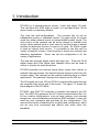
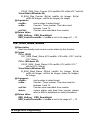
the computer case at the rear of the board. The figure 1.1 shows the
block diagram of the PCI-8554.
PCI-8554 uses SAIC PCI controller to interface the board to the PCI
bus. The ASIC fully implement the PCI local bus specification Rev 2.0.
All bus relative configurations, such as base memory and interrupt
assignment, are automatically controlled by BIOS software. It does not
need any user interaction and pre-study for the configurations. This
removes the burden of searching for a conflict-free configuration, which
can be very time consuming and difficult with some other bus
standards.
Introduction 1
Software Supporting:
There are several software options help you get your application
running quickly and easily.
Custom Program :
For the customer who is writing their own programs, the PCI-8554 is
supported by a comprehensive set of drivers and programming tools.
These software supports are available in multiple platforms.
.
MS-DOS Borland C/C++ program library.
.
DLL: Dynamic Linking Library for Win-95
.
PCIS-DASK/NT: DLL software developing kit for Win-NT (optional)
Address
bus
PCI Bus
Interrupt
PCI
Controller
8254
chip #1
8254
chip #2
Interrupt
system
COUT12
clock
system
8
8
COUT1 ~ COUT3
GATE1 ~ GATE3
COUT4 ~ COUT6
GATE4 ~ GATE6
8254
chip #3
COUT7 ~ COUT9
GATE7 ~ GATE9
8254
chip #4
COUT10 only
GATE10 only
Debounce
system
100 pin SCSI-II
8bits digital
input/output
data
bus
ECLK1 ~ ECLK10
E_INT
Figure 1.1. Block diagram of the PCI-8554
1.1. Features
The PCI-8554 Counter / Timer and digital I/O Card provides the following
advanced features:
• Four 8254 chips provide twelve 16 bits down counters
• Multi-configurations of counters / timers:
• Flexible setting for each independent counter, the clock source could
be external, internal or cascaded. The gate signal is external
controlled or internal enabled.
2 • Introduction
•
•
•
•
•
•
Provide debounce function with flexible setting to prevent from
bounce phenomenon when using external clock.
8 digital output channels
8 digital input channels
Dual interrupt sources
The first interrupt source comes from output of counter #12
The second interrupt source comes from external source.
100-pin SCSI-II female connector.
PCI-Bus
1.2. Applications
Event counter
Frequency generator
Frequency synthesizer
Pulse width measurement
Low level pulse generator
Time delay
Industry automation
Watchdog timer
1.3. Specifications
♦ Programmable Counter / Timer
• Device : 8254x 4
• Counters : 16-bit down counter
• Clock source : internal clock, external source or cascaded
• Gate control : default enable or external control
♦ Digital I/O ( DIO)
• # of input channels : 8 channels
• # of output channels : 8 channels (dedicated output)
• Electronics characteristics : TTL compatible signal
♦ General Specifications
• I/O Base Address : 32 consecutive address ( 32 bits ) in the PCI I/O
address space
• Connector : 100-pin SCSI-II female connector
• Operating Temperature : 0° C ~ 60° C
• Storage Temperature : -20° C ~ 80° C
• Humidity : 5 ~ 95%, non-condensing
Introduction • 3
•
•
Power Consumption : +5 V @ 300 mA maximum
Dimension : 134mm(L) X 108mm(W)
4 • Introduction
2. Installation & Configurations
This chapter describes the configurations and multi-functions of the
PCI-8554 and teach user to install PCI-8554. At first, the contents in
the package and unpacking information that you should care about are
described, then versatile configurations of PCI-8554 are introduced so
that you can configure it according to your applications. The default
jumper setting of PCI-8554 is shown in this chapter also.
2.1. What You Have
In addition to this User's Manual, the package includes the following
items:
•
•
PCI-8554 Enhanced Multi-function Counter / Timer Card
Utility & Library Diskette
If any of these items is missing or damaged, contact the dealer from
whom you purchased the product. Save the shipping materials and
carton in case you want to ship or store the product in the future.
2.2. Unpacking
Your PCI-8554 card contains sensitive electronic components that can
be easily damaged by static electricity. The card should be unpacked
on a grounded anti-static mat. The operator should be wearing an antistatic wristband, grounded at the same point as the anti-static mat.
Inspect the card module carton for obvious damage. Shipping and
handling may cause damage to your module. Be sure there are no
shipping and handing damages on the module before processing.
After opening the card module carton, extract the system module and
place it only on a grounded anti-static surface component side up.
Again inspect the module for damage. Press down on all the socketed
IC's to make sure that they are properly seated. Do this only with the
module place on a firm flat surface.
Installation & Configuration • 5
Note : DO NOT APPLY POWER TO THE CARD IF IT HAS BEEN
DAMAGED.
You are now ready to install your PCI-8554.
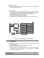
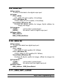
2.3. PCB Layout of PCI-8554
This layout will be modified after jumper layout finished.
U17
CN1
U10
U18
U11
U6
Timer/
Counter
8254 #4
U3
Timer/
Counter
8254 #1
U14
U15
U4
Timer/
Counter
8254 #2
U5 PCI-8554
Timer/
Counter
8254 #3
U16
U12
U20
PCI Connector Chip
U13
U21
U19
U7
U8
8MHz
U9
U2
U1
Figure 2.1 PCB Layout of PCI-8554
2.4. Default Configurations
To operate the PCI-8554 correctly, users should understand the
structure of PCI-8554 and details of the possible configurations. The
block diagram of the PCI-8554 is shown in chapter 1. It contains the
clock system, counters confederation, interrupt system and PCI
controller. The following sections teach you the jumper setting and the
default setting listed in Table 2.1.
6 • Installation & Configuration
Items
ECLK1
ECLK2
ECLK3
ECLK4
ECLK5
ECLK6
ECLK7
ECLK8
ECLK9
ECLK10
E_INT
Default Configuration
Setting by:
No debounce function
JP1
No debounce function
JP2
No debounce function
JP3
No debounce function
JP4
No debounce function
JP5
No debounce function
JP6
No debounce function
JP7
No debounce function
JP8
No debounce function
JP9
No debounce function
JP10
No debounce function
JP11
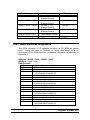
Table 2.1 Default Configuration of PCI-8554
There are eleven jumpers on PCI-8554, these jumpers are used to
select debounce function. You can change PCI-8554's default
configuration by setting jumpers on the card for your own applications.
The card's jumpers are preset at the factory.
Before changing the default configuration, users must fully understand
the operation of the debounce function. The setting and the basic
operation theorem are not discussed in this chapter.
It is
recommended to refer chapter 2.12 for details of the operation theorem
and to refer chapter 4 for application notes.
2.5. PCI-8554 Installation Outline
PCI-8554 support plug and play , the card can requests memory usage
(I/O port locations) assigned by system BIOS. The address assignment
is done on a board-by-board basis for all PCI-8554 in the system.
Your computer will probably have both PCI and ISA slots. Do not force
the PCI-8554 into a PC/AT slot.
Installation Procedures :
1. Turn off your computer
2. Turn off all accessories (printer, modem, monitor, etc.) connected
to computer.
3. Remove the cover from your computer.
4. Select a 32-bit PCI expansion slot. PCI slot are short than ISA or
Installation & Configuration • 7
5.
6.
7.
EISA slots and are usually white or ivory.
Before handling the PCI-8554, discharge any static buildup on
your body by touching the metal case of the computer. Hold the
edge and do not touch the components.
Position the board into the PCI slot you selected.
Secure the card in place at the rear panel of the system unit using
screw removed from the slot.
Running the 8554UTIL.EXE :
A testing program is included in this utility, you can check if your PCI
card work properly by this file.
2.6. Pin Assignment of Connector
(1)
(2)
(3)
(51)
(52)
(53)
(48)
(49)
(50)
(98)
(99)
(100)
(1) +12V
(2) +12V
(3) +12V
(4) Vcc
(5) Vcc
(6) Vcc
(7) NC
(8) DI_6
(9) DI_4
(10) DI_2
(11) DI_0
(12) DO_6
(13) DO_4
(14) DO_2
(15) DO_0
(16) NC
(17) GND
(18) GND
(19) GND
(20) GND
(21) GND
(22) GND
(23) GND
(24) GND
(25) GND
(26) GND
(27) GND
(28) GND
(29) GND
(30) GND
(31) GND
(32) GND
(33) GND
(34) GND
(35) GND
(36) GND
(37) GND
(38) GND
(39) GND
(40) GND
(41) GND
(42) GND
(43) GND
(44) GND
(45) GND
(46) GND
(47) GND
(48) GND
(49) GND
(50) GND
(51) GND
(52) GOUT2
(53) GIN2
(54) GND
(55) GOUT1
(56) GIN1
(57) E_INT
(58) DI7
(59) DI5
(60) DI3
(61) DI1
(62) DO7
(63) DO5
(64) DO3
(65) DO1
(66) NC
(67) COUT12
(68) GND
(69) GOUT11
(70) GND
(71) COUT10
(72) GATE10
(73) ECLK10
(74) COUT9
(75) GATE9
Legend:
ECLK n
: External clock source for counter #n
8 • Installation & Configuration
(76) ECLK9
(77) COUT8
(78) GATE8
(79) ECLK8
(80) COUT7
(81) GATE7
(82) ECLK7
(83) COUT6
(84) GATE6
(85) ECLK6
(86) COUT5
(87) GATE5
(88) ECLK5
(89) COUT4
(90) GATE4
(91) ECLK4
(92) COUT3
(93) GATE3
(94) ECLK3
(95) COUT2
(96) GATE2
(97) ECLK2
(98) COUT1
(99) GATE1
(100) ECLK1
ExtG n
COUT n
DO_m
DI_ m
E_int
GOUT1
GOUT2
: External gate signal for counter #n
: Counter / Timer output of counter #n
: Digital output port channel #m
: Digital input port channel #m
: External interrupt signal input
: Inverse TTL signal of GIN1
: Inverse TTL signal of GIN2
Figure 2.2 Pin Assignment of Connector CN1
2.7.Clock System
The clock system of PCI-8554 provides the internal clock source for the
8254 chips. The clock of counter / timer #1 ~ #10 can be one of the 4
sources: external clock source or cascaded source from the ‘last’
channel or CK1 or COUT10. The next section will give you detail
description about setting clock for each counter / timer and definition of
CK1. The clock of counter / timer #11 is fixed at 8Mhz, and clock of
counter / timer #12 is connected to COUT11
2.8.Counters Architecture
There are four 8254 chips on PCI-8554 card. The counters on chip #1
~ #4 are labeled from counter #1 to counter #12. Counters #11 and
#12 are cascaded counters, and counter #1~ #10 can be
programming to independent or cascaded counters. Table 2.2
illustrates the relationship between the reference number of chips and
the counters number.
Installation & Configuration • 9
8254 Chip Reference
Number
Number
Chip #1
U3
Chip #2
U4
Chip #3
U5
Chip #4
U6
Counter
Number
Counter #1
Counter #2
Counter #3
Counter #4
Counter #5
Counter #6
Counter #7
Counter #8
Counter #9
Counter #10
Counter #11
Counter #12
Type of
Counter
Independent or Cascaded
Independent or Cascaded
Independent or Cascaded
Independent or Cascaded
Independent or Cascaded
Independent or Cascaded
Independent or Cascaded
Independent or Cascaded
Independent or Cascaded
Independent or Cascaded
Cascaded
Cascaded
Table 2.2 Counters Architecture
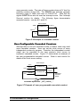
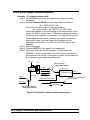
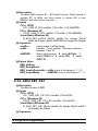
There are three signals (2 input,1 output) for each counter, a clock
input signal, a gate control signal, and an output signal. The Figure 2.3
illustrates the block diagram of 8254 counter. CLK1 ~ CLK12 are
clock sources and GATE1 ~ GATE12 are gate control signals. The
COUT1 ~ COUT12 are output of the counters. The Figure 2.4 shows
all the labels and the inter-connection of the 8254 counters.
8254 Chip
Clock Source Input
C
Gate Control Input
Counter
Counter / Timer Output
O
G
Figure 2.3 Block Diagram of 8254 Counter
10 • Installation & Configuration
8254 Chip #2
8254 Chip #1
CLK4
CLK1
C
GATE4
Counter #4
C
COUT4
O
GATE1
COUT1
Counter #1
O
Counter #2
O
Counter #3
O
G
G
CLK2
CLK5
C
GATE5
Counter #5
O
C
COUT5
GATE2
COUT2
G
G
CLK3
CLK6
C
GATE6
Counter #6
C
COUT6
O
GATE3
COUT3
G
G
8254 Chip #4
8254 Chip #3
CLK10
CLK7
C
GATE10
G
C
COUT10
Counter #10
O
GATE7
G
COUT7
Counter #7
O
Counter #8
O
Counter #9
O
CLK8
8M Hz
C
'H' G
COUT11
C
COUT11
Counter #11
O
Counter #12
O
GATE8
G
COUT8
CLK9
C
'H' G
C
COUT12
GATE9
G
COUT9
Figure 2.4 Counters Architectural
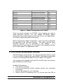
Independent Counters (Counter #1~#10)
The Counter #1 to Counter #10 are independent counters because the
clock source and gate control of those counters can be set
independently. These 10 counters are named as independent counter.
8254 Chip #1
CLK1
C
GATE1
Counter #1
COUT1
O
G
Figure 2.5 Example of ‘independent counters’
Cascaded Counters
The connection of Counter #11 and #12 are different from other
independent counters. These two counters are named as cascaded
counters because the clock sources of counter #11 come from fixed 8
MHz and its output are cascaded to counter #12. In fact, counter
#11and #12 are designed for frequency divider by using 8254's square
Installation & Configuration • 11
wave generator mode. The gate of these counters keep at 'H' level for
enabling counters all the time. The COUT12 can precisely generate
frequency upper to 2MHz and lower to 0.00186 Hz. Note that the
signals COUT12 can also be used as interrupt source. See ‘Interrupt
Sources’ section for details.
The following figure demonstrates
cascaded counter - counter #11 and #12.
8254 Chip #4
8 MHz
C
COUT11
Counter #11
O
Counter #12
O
'H' G
COUT11
C
COUT12
'H' G
Figure 2.6 Example of ‘cascaded counter’
User Configurable Cascaded Counters
Although there is one set cascaded counter on board, users may need
more cascaded counters. User can set the clock source of every
independent counters by program. Therefore, the independent counter
output can be cascaded to the next counter's clock source to
implement cascaded counter. Figure 2.7 demonstrate an example of
the user programmable cascaded counter. Refer to next section for
details of the clock source setting.
8254 Chip #1
CLK1
C
GATE1
COUT1
Counter #1
O
Counter #2
O
G
VCC
CLK2
C
GATE2
VCC
COUT2
G
Cascaded
Counters
Output
selectable by function "_SET_cntCLK_ "
Figure 2.7 Example of ‘user programmable cascaded counters’
12 • Installation & Configuration
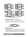
2.9. Clock Source Configurations
For every independent counter, four signals can be chosen as clock
source by software . The clock source of counter #n comes from either
external clock source (ECLK n) or the cascaded counter output
(COUTn-1) or CK1 or COUT10. ( Note : 1.The clock source of the
cascaded counters #11 is fixed to C8M and counter #12 is fixed to
COUT11 2.The external clock source named as ECK n comes from
jumper JP1 ~ JP10, please see section 2.12 for detail description. )
n=1~9
ECK n
COUT n-1
CK1
COUT10
CLK n
select by function
"_8554_SET_cntCLK"
ECK10
COUT9
CK1
C8M
CLK10
select by function
"_8554_SET_cntCLK"
Figure 2.8 Clock Source of Counter #n
C8M
CK1
COUT11
select by function
"_8554_SET_CK1"
Figure 2.9 Clock Source of CK1
The internal clock sources CK1 comes from the clock system C8M or
COUT11, selected by function “_8554_SET_CK1”, and counters can be
set to cascaded mode, then clock source comes from the output of the
counter with smaller channel number. For example, the COUT1 is
cascaded to CLK2, the COUT3 is cascaded to CLK4. ( Note : If
counter #1 is set to cascaded mode, CLK1 is connected to GND
because COUT0 doesn’t exist. )
Installation & Configuration • 13
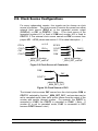
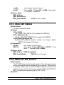
2.10. Gate Control Configurations
The gate control signals of the independent counters are internally
pulled high hence they are default enable if no external gate used.
When the external gate signals are used, the counters can be used to
measure pulse width. Therefore, the time interval of the counter gate
can be precisely controlled and frequency measurement is possible.
Figure 2.10 shows the jumper setting of gate control of counter #1~
#10. ( Note : The gate control of counter #11 and #12 are always
enable. )
VCC
GATE n( From 100 pin
SCSI-II Connector )
GATE n( To 8254 )
Figure 2.10 Gate source of counter #1 ~#10
2.11. Counter Outputs
The timer / counter output signals (COUT n) of 8254 are controlled by
clock source, gate control and software programming. All the output of
the 12 counters are sent to the 100 pins connector directly, please see
'Pin assignment' for corresponding signal pin number.
In addition, the output signal may be used as clock source for
cascaded counters, see the above sections. It is possible to cascaded
ten counters by software setting, see 2.8 for reference. The counters
output COUT12 is also used as internal interrupt source (refers to
'Interrupt System').
2.12. Debounce System
Debounce system is used to eliminate bounce phenomenon. If external
clock is used, user can set jumper JP1 ~ JP11 to select if debounce
system is used or not used. If debounce system is used, the debounce
output signal will be the same state as the input only if the input signal
14 • Installation & Configuration
keep the same state for four DB_CLK, otherwise the input signal will
be treated as glitch and the debounce output signal will keep previous
state, figure 2.11 show you the how to set these jumpers, figure 2.12
show you how to select DB_CLK, figure 2.13 show you the basic
theorem of debounce system.( Note : DB_CLK can’t be higher than
2MHz. )
ECLK n
debounce
system
DB_CLK
n=1~10
JP n
E_INT
JP11
debounce
system
ECK n
EXTINT
DB_CLK
Figure 2.11 Structure of JP1 ~ JP11
COUT11
DB_CLK
2MHz
select by function
"_8554_SET_DBCLK"
Figure 2.12 Clock Source of DB_CLK
DB_CLK
input
signal
output
signal
glitch is
eliminated
Figure 2.13 Basic theorem of debounce system
Installation & Configuration • 15
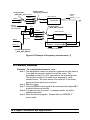
2.13. Interrupt System
The PCI-8554‘s interrupt system is a powerful and flexible system,
which is suitable for many applications. The system is a Dual Interrupt
System. The dual interrupt means the hardware can generate two
interrupt request signals at the same time and the software can service
these two request signals by ISR. Note that the dual interrupt do not
mean the card occupy two IRQ levels. These two interrupt request
signals (INT1 and INT2) comes from external interrupt signal EXTINT
and the timer / counter #12 output. Fig 2.14 show you the structure of
interrupt system.
Clear by "8554_CLR_IRQ1"
8254 Chip #4
8MHz
8254 Chip #4
C
'H'
Counter #11
C
O
G
'H'
Counter #12
COUT12
O
G
IRQ
FlipFlops
INT1
E_INT
JP11
debounce
system
EXTINT
IRQ
FlipFlops
INT2
PCI
Controller
INT #A
DB_CLK
Clear by "8554_CLR_IRQ2"
Fig 2.14 Dual Interrupt System of PCI-8554
There is only one IRQ level used by this card although it is a dual
interrupt system. This card uses INT #A interrupt request signal to PCI
bus. The mother board circuits will transfer INT #A to one of the AT
bus IRQ levels. The IRQ level is set by the PCI plug and play BIOS
and saved in the PCI controller. It is not necessary for users to set the
IRQ level. Users can get the IRQ level setting by software library.
Refer the section 5.4.
The PCI controller of PCI-8554 can receive two hardware IRQ sources.
However, a PCI controller can generate only one IRQ to PCI bus, the
two IRQ sources must be distinguished by ISR of the application
16 • Installation & Configuration
software if the two IRQ are all used. The application software can use
the “_8554_GET_IRQ_Status” function to distinguish which interrupt is
inserted and servicing that IRQ then users must clear current IRQ to
allow the next IRQ coming in.
If the application need only one IRQ, you can disable one of the IRQ
sources by software. If your application do not need any IRQ source,
you can disable both the two interrupts . However, the PCI BIOS still
assign a IRQ level to the PCI card and occupy the PC resource if you
only disable the IRQ sources without change the initial condition of the
PCI controller. It is not suggested to re-design the initial condition of
the PCI card by users‘ own application software. If users want to
disable the IRQ level, user can use the ADLink’s utility ‘INIT8554.EXE’
to change power on interrupt setting.
2.14. Digital Input and Output
To program digital I/O operation is fairly straight forward. The digital
input operation is just to read data from the corresponding registers,
and the digital output operation is to write data to the corresponding
registers. The digital I/O registers‘ format are shown in section 3.4 and
3.5.
2.15. 12V and 5V Power Supply
The 100 pin SCSI-II connector provides +12 volts and +5 volts power.
To avoid short or overload of the power supply, the fuses are added on
all the power supply signals. The maximum current for 5 volts on
every fuse is 0.5 A. If the load current is larger than 0.5 A, the
resistance of the fuse will increase because of the temperature rising.
The rising resistance will cause the power supply drop and reduce
current. If the overload or short condition is removed, the fuse will
return to normal condition. It is no necessary to repair or re-install the
fuse.
The maximum current of 12 volts for all the four connectors is also 0.5
A. The action of the fuse is the same as which used for +5V power.
The limitation is more restrict than 5V power supply because the PCI
bus can not provide large current.
Installation & Configuration • 17
3. Registers Format
The detailed descriptions of the register format of the PCI-8554 are
specified in this chapter. This information is quite useful for the
programmers who wish to handle the card by low-level programming. In
addition, users can understand how to use software driver to manipulate
this card after understanding the registers' structure of the PCI-8554.
3.1. I/O Port Address
The PCI-8554 requires 32 consecutive addresses in the PC I/O address
space. Table 3.1 shows the I/O address of each register with respect to
the base address. The PCI-8554 functions as a 32-bit PCI target device
to any master on the PCI bus. There are three types of registers on the
PCI-8554: PCI Configuration Registers (PCR), Local Configuration
Registers (LCR) and PCI-8554 registers.
The PCR which conforms the PCI-bus specifications Rev2.1 are
initialized and controlled by the system plug & play PCI BIOS. Users can
study the PCI BIOS specifications to understand the operation of the
PCR. The PCR can only be read through by PCI BIOS function call.
Please refer to the PCI specifications for the details of the PCR, and refer
to the PCI BIOS specifications for the standard BIOS function calls. You
can also get the PCR register format from the data sheet of the PCI bus
controller: PLX technology’s PCI-9050.
The LCR are specified by the PCI bus controller PCI-9050. It is not
necessary for users to understand the details of the LCR if you use the
software library. The base address of the LCR is assigned by the PCI
PnP BIOS. The assigned address is located at offset 14h of PCR.
The PCI-8554 registers are shown in the Table 3.1. The base address of
the PCI-8554 registers is also assigned by the PCI PnP BIOS. The
assigned base address is located at offset 18h of PCR. Note that most
of the PCI-8554 registers are 8 bits. The users can access these
registers by 8 bits I/O instructions.
Users can read the PCR to get the LCR base address and the two PCI8554 base addresses by using the PCI BIOS function call.
Register Format • 18
I/O Address
Base + 0x00 ~ 0x03
Write
Read
Counter 1 ~ 3
Counter 1 ~ 3
& Mode Control
Base + 0x04 ~ 0x07
Counter 4 ~ 6
Counter 4 ~ 6
& Mode Control
Base + 0x08 ~ 0x0B
Counter 7 ~ 9
Counter 7 ~ 9
& Mode Control
Base + 0x0C ~0x0F
Counter 10 ~ 12
Counter 10 ~ 12
& Mode Control
Base + 0x10 ~ 0x12
Clock Mode Control
-Base + 0x18
Digital Output
Digital Input
Table 3.1. I/O Address Map of PCI-8554
3.2.Timer/Counter Registers
The 8254 occupies 4 I/O address locations in PCI-8554 as shown
blow. Users can refer to Tundra's or Intel's data sheet for a full
description of the 8254 features, condensed information is specified in
Appendix A.
Address : BASE + 0x00 ~ BASE + 0x0F
Attribute : read / write
Data Format :
Base + 0
Base + 1
Base + 2
Base + 3
Base + 4
Base + 5
Base + 6
Base + 7
Base + 8
Base + 9
Base + A
Base + B
Base + C
Base + D
Base + E
Base + F
Counter 1 Register ( R/W)
Counter 2 Register ( R/W)
Counter 3 Register ( R/W)
8254 Mode Control Register (W)
8254 Read Back Register (R)
Counter 4 Register ( R/W)
Counter 5 Register ( R/W)
Counter 6 Register ( R/W)
8254 Mode Control Register (W)
8254 Read Back Register (R)
Counter 7 Register ( R/W)
Counter 8 Register ( R/W)
Counter 9 Register ( R/W)
8254 Mode Control Register (W)
8254 Read Back Register (R)
Counter 10 Register ( R/W)
Counter 11 Register ( R/W)
Counter 12 Register ( R/W)
8254 Mode Control Register (W)
8254 Read Back Register (R)
Register Format • 19
3.3.Timer / Counter Clock Mode Control
There are total twenty two bits on PCI-8554 to select clock source of
Timer / Counter #1 ~ #10 and CK1 and debounce clock.
Address : BASE + 0x10 ~ 0x12
Attribute : write only
Data Format :
Bit
Base+0x10
Base+0x11
Base+0x12
CnN1
7
6
5
4
3
2
1
0
C1N1 C2N1 C3N1 C4N1 C4N2 C3N2 C2N2 C1N2
C5N1 C6N1 C7N1 C8N1 C8N2 C7N2 C6N2 C5N2
C9N1 C10N1 CK1SEL DBCSEL
C10N2 C9N2
CnN1 : these two bits are used to control clock source of Timer /
Counter n, n = 1 ~ 10
CK1SEL :
select source of CK1
DBCSEL :
select debounce clock
3.4.Digital Input Registers
There are 8 digital input channels on the PCI-8554.
Address : BASE + 0x18
Attribute : read only
Data Format :
Bit
Base+0x18
7
DI7
6
DI6
5
DI5
4
DI4
3
DI3
2
DI2
1
DI1
0
DI0
The register is a general purpose 8 bits digital output port.
signals can be used to control external devices.
These
3.5.Digital Output Register
Address : BASE + 0x18
Attribute : write only
Data Format :
Bit
Base+0x18
7
6
5
4
3
2
1
0
DO7
DO6
DO5
DO4
DO3
DO2
DO1
DO0
20 • Register Format
4. Signal Connections & Applications
This chapter describes the connectors and some application of the
PCI-8554. including the signal connection between the PCI-8554 and
external devices
4.1.Connectors Pin Assignment
The PCI-8554 comes equipped with a 100 pin SCSI-II female
connector (CN1). The CN1 is located at the rear plate. The pin
assignment of the connector is illustrated in the Figure 2.1. . Refer to
section 2.1 for details of pin assignment.
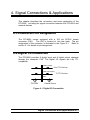
4.2.Digital I/O Connection
The PCI-8554 provides 8 digital input and 8 digital output channels
through the connector CN1. The digital I/O signals are fully TTL
compatible.
Digital Input(DI)
From TTL Devices
Digital Output (DO)
To TTL Devices
GND
ACL-8454
PCI-8554
Outside Device
Figure 4.1 Digital I/O Connection
Signal Connection and Applications • 21
4.3.Timer / Counter Connection
The PCI-8554 has four 8254 chips on board. It can offer 10
independent 16-bit programmable down counters and cascaded
counters. To implement your application, you can following the
procedure to design your application and connect the signals.
1.
2.
3.
4.
5.
Check if use a clock source with fixed frequency, if answer is ‘No’,
external clock source must be used and go to step 3.
Calculate the frequency of clock according to your application
and decide the clock source: internal, external, or cascaded,
then decide which counter is used.
If external clock source is used, generate a clock source outside
the board and check the frequency. If external clock source is
used, you have to decide whether debounce function is used or
not, and then set the jumper JP1 ~ JP10.
Decide the gate control source: always enable or externally
control, if gate control is necessary, connect the gate signal
Program the counter / timer using desired mode.
4.4.Frequency Generator
Example 1 : To generate a 250 K Hz Square Wave.
step 1: To use fixed clock source because the output is a fixed
frequency.
step 2: Internal 8M Hz is suitable to generate 250K Hz frequency.
Use Counter #1 for this application.
250 kHz = 8 M Hz / 32
step 3: Skip these steps.
step 4: The gate source is enable always, so let SCCI-II connector
pin99 GATE1 open
step 5: Connect the counter output to external device and write the
control program. Please refer the ‘DEMO1.C’ source code.
set by function
"_8554_SET_CK1"
8MHz
COUT11
ECK1
set by function "8554_SET_cntCLK"
GND
CK1
COUT10
22 • Signal Connection and Applications
8254 Chip #1
C
'H'
G
Counter #1
COUT1
O
Figure 4.2 Example of frequency generator (1)
Example 2 : To generate a very low frequency of 1 pulse / 1 hour
step 1: To use fixed clock source because the output is a fixed
frequency.
step 2: Because the desired frequency (1/3600sec=0.000278Hz) is
too slow to use one counter to generate, set the independent
counter #1 & #2 & #3 to cascade mode : Clock source of
counter #1 comes from C8M, clock source of counter #2
comes from COUT1, clock source of counter #3 comes from
COUT2. Divider value of counter #1 was set to 4000, divider
value of counter #2 was set to 2000, divider value of counter
#3 was set to 3600, 8MHz/4000/2000/3600 = 1/3600, so
COUT3 will generate a pulse every hour.
step 3: Skip these steps.
step 4: The gate source is enable always, so let GATE1 GATE2
GATE3 open.
step 5: Write and verify the control program. Please refer the
‘DEMO2.C’ source code.
set by function
"_8554_SET_CK1"
8MHz
COUT11
ECK1
GND
CK1
COUT10
ECK2
COUT1
CK1
COUT10
ECK3
COUT3
CK1
COUT10
set by function "8554_SET_cntCLK"
8254 Chip #1
C
'H'
Counter #1
COUT1
O
G
set by function "8554_SET_cntCLK"
8254 Chip #1
C
'H'
Counter #2
COUT2
O
G
set by function "8554_SET_cntCLK"
8254 Chip #1
C
'H'
Counter #3
O
COUT3
G
Figure 4.3 Example of frequency generator (2)
Signal Connection and Applications • 23
4.5.Pulse Width Measurement
Example : To measure pulse width
step 1: To use fixed clock source as base time interval (or base
frequency).
step 2: Assume Internal 2M Hz clock is used. The time base is
∆ t = 1/2M=5x10e-7 sec
The count range for measuring pulse width is:
∆ t < pulse width < ∆ t *65535 (=32.768 msec)
If the specification of the pulse width to be measured is in the
range, the 2M Hz can be used. Otherwise changing the base
frequency of the counter, for example, you can set counter #2
to cascaded counter mode, and use counter #2 to measure
pulse width, then the count range can increase but the
resolution will decrease. Counter #1 #2 #3 are used in this
example.
step 3: Skip these steps.
step 4: Connect GATE1 to the signal to be measured.
step 5: Write and verify the control program. Please refer the
‘DEMO3.C’ source code. Note that if the pulse is shorter, the
time resolution is worse. If the pulse is wider, the limitation of
the maximum pulse width should be care.
ECLK1
JP1
debounce
system
set by function
"_8554_SET_cntCLK"
ECK1
8254 Chip #1
GND
C
CK1
COUT10
2MHz
Counter #1
COUT1
O
G
DB_CLK
Signal to be measured
Polling D/I for checking the
end of a pulse
COUT11
Pulse Width
selectable by function
"_8554_SET_DBCLK"
Figure 4.4 Example of pulse width measurement
24 • Signal Connection and Applications
4.6.Frequency Measurement
Example : To measure frequency around 1~100 K Hz
step 1: This application need two counters. One counter is used to
generate a pulse whose time interval is very precise. The
pulse is used to enable the other counter (counting counter) by
gate control. The gate control is coming from /COUT3. In
this example, cascaded counter is used, the pulse generator is
counter #3 ( clock is from COUT2 ) and the counter #1 is used
to measure frequency.
step 2: The maximum value of counting counter is no more than
65535, For measuring 100 K Hz frequency, the time interval
should be within 1/100 K Hz x 65535 = 0.655 sec. If the time
interval is wider, then the measurement resolution is better,
however, the counting value will be overflow if time interval is
too long. That means the low pulse width of counter #3 output
should shorter than 0.655 sec. User can try to generate the
pulse by counter #3 by yourself.
step 3: Connect the signal to be measured to the ECLK1 and adjust
JP1 to select debounce function.
step 4: Connect GATE1 to /COUT3.
step 5: The following block diagram illustrates the application. Write
and verify the control program. The frequency of the signal is
:
frequency = counting value of counter #1 / precise time interval
Please refer the ‘DEMO4.C’ source code.
Signal Connection and Applications • 25
set by function
"_8554_SET_CK1"
8MHz
COUT11
set by function
"_8554_SET_cntCLK"
Precise
Time
Interval
ECK2
8254 Chip #1
COUT1
CK1
COUT10
ECLK1
( frequency to
be measured )
C
'H'
O
COUT2
G
JP1
debounce
system
Counter #2
set by function
"_8554_SET_cntCLK"
ECK1
8254 Chip #1
GND
CK1
COUT10
C
Counter #1
COUT1
O
G
DB_CLK
2MHz
/COUT2
COUT11
connect by user
'H' enable counter #1
selectable by function
"_8554_SET_DBCLK"
Figure 4.5 Example of frequency measurement (1)
4.7.Event Counter
Example : To count external event in 1 sec
step 1: This application needs one counter to generate a time base of
1 sec and the second counter to count the event. The
cascaded counter #11, #12. can perform the watchdog timer.
The another counter #1 is used as an example to count
external event. The clock source of counter #1 is the event
signal and the frequency is not fixed.
step 2: Skip this steps.
step 3: Connect ECLK1 to the signal to be measured and adjust JP1
to select debounce function.
Step 4: The gate source of counter 1 is always enable, so let the
external gate open.
step 5: Write the control program. Please refer the ‘DEMO5.C’
source code.
26 • Signal Connection and Applications
ECLK1
( Event Signal )
ECK1
debounce
system
2MHz
selectable by
function
JP1
8254 Chip #1
GND
CK1
COUT10
C
'H'
Counter #1
COUT1
O
G
DB_CLK
COUT11
selectable by function
"_8554_SET_DBCLK"
8254 Chip #4
8MHz
C
'H'
G
8254 Chip #4
Counter #11
C
O
'H'
Counter #12
COUT12
O
G
Figure 4.6 Example of event counter
Signal Connection and Applications • 27
4.8.Dual Interrupt System
One Internal plus one external interrupt sources
The PCI-8554 provides double interrupt sources which is very useful in
some application. For example, most of the application needs a
watchdog timer to monitor the system periodically, hence, an IRQ
channel is used. In addition, the emergency control may be necessary,
hence, an additional external IRQ channel is helpful to handle the
situation. Therefore, dual interrupt level is necessary.
Clear by "8554_CLR_IRQ1"
8254 Chip #4
8MHz
8254 Chip #4
C
'H'
Counter #11
C
O
G
'H'
Counter #12
COUT12
O
G
IRQ
FlipFlops
INT1
E_INT
JP11
debounce
system
EXTINT
IRQ
FlipFlops
INT2
PCI
Controller
DB_CLK
Clear by "8554_CLR_IRQ2"
Figure 4.7 Example of dual interrupt system
28 • Signal Connection and Applications
INT #A
5. High-Level Programming
There are 10 functions provided by the C language library. By using
the C language library, it saves a lot of programming time.
If you need to perform some special functions which are not provided
in the library, you can modify the library according to your requirement.
The fully commented C source of the library is also included in your
software library diskette. It is a good starting point for C language
programmers who wish to modify the functions in the library.
In addition to library and source code, some demonstrating programs
are also included in the disk. It will help you to understand the library
more quickly.
Please refer the demonstration examples in the diskette to get
examples of the using of the library
5.1.Installation
The Utility Software and Library supplied with PCI-8554 is in DOS
format which is compatible with DOS 3.0 or higher versions. It is
advisable to make a back up copy before using the software.
For a direct back up, use the DOS DISKCOPY or alternatively
XCOPY *.* to a pre-formatted disk. The back up procedures are
specified as follows:
1. Insert "PCI-8554 Library & Utility" diskette into floppy drive A:
2. XCOPY a:*.* b:/s
The PCI-8554's Library & Utility diskette includes a utility software,
C-language library and some demonstration programs which can
help you reduce programming work.
♦ MS-DOS Software Installation
1. Turn your PC's power switch on
29 • High Level Programming
2. Put the "PCI-8554 Library & Utility" diskette into your floppy
drive A: or B:
3. Execute the following command under DOS environment:
A:\> CD \DOS
A:\DOS> SETUP
4. An installation completed message will be shown on the
screen.
♦ Windows 95 Software Installation
1. Turn your PC's power switch on and enter Windows 95
2. Put the "PCI-8554 Library & Utility" diskette into your floppy
drive A: or B:
3. execute A:\Win95\Setup.exe
(PCI-8554 is a plug & play card, so please following the
standard Win-95 convention to install hardware driver
Pci8554.inf. This file is included in this diskette.)
5. Re-start the Windows 95.
5.2. Running Testing Utility (8554UTIL.EXE)
After finishing the DOS installation, you can execute the utility by typing
as follows :
C> cd \8554\DOS\UTIL
C> 8554UTIL
5.3.Software Driver Naming Convention
The functions of PCI-8554's software drivers are using full-names to
represent the functions' real meaning. The naming convention rules are
:
In DOS Environment :
_{hardware_model}_{action_name}. e.g. _8554_Initial().
30 • High Level Programming
In order to recognize the difference between DOS library and Windows
95 library, A capital "W" is put on the head of each function name of the
Windows 95 DLL driver. e.g. W_8554_Initial().
There are 10 functions provided by PCI-8554 software drivers. The
detail descriptions of each function are specified in the following
sections. The functions prototype and some useful constants are
defined in Acl_pci.h.
5.4._8554_Initial
@ Description
The PCI-8554 cards are initialized by this function. The software
library could be used to control multiple PCI-8554 cards.
Because PCI-8554 is in PCI bus architecture and meets the plug
and play specifications, the IRQ and I/O address are assigned
by system BIOS directly.
@ Syntax
C/C++ (DOS)
U16 _8554_Initial (U16 *existCards, PCI_INFO *pciinfo)
C/C++ (Windows 95)
U16 W_8554_Initial (U16 *existCards, PCI_INFO *pciinfo)
Visual Basic (Windows 95)
W_8554_Initial (existCards As Integer, pciInfo As PCI_INFO)
As Integer
@ Arguments
existCards : The numbers of installed PCI-8554 cards. The
returned value shows how many PCI-8554 cards
are installed in your system.
pciinfo :
It is a structure to memorize the PCI bus plug
and play initialization information which is
decided by PnP BIOS. The PCI_INFO
structure is defined in PCI_8554.H. The base
I/O address and the interrupt channel number is
stored in pciinfo which is for reference.
@ Return Value
ERR_NoError, ERR_PCIBiosNotExist
High Level Programming • 31
5.5._8554_Write_Counter
@ Description
User can directly write command to counter #1 ~ #12 by this
function. Using this function, user can assign the counter
number 1~12 directly without care about the chips number and
other details.
@ Syntax
C/C++ (DOS)
U16 _8554_Write_Counter (U16 cardNo, U16 cntNo, U16 mode,
U16 cntrVal)
C/C++ (Windows 95)
U16 W_8554_Write_Counter (U16 cardNo, U16 cntNo, U16 mode,
U16 cntrVal)
Visual Basic (Windows 95)
W_8554_Write_Counter (ByVal cardNo As Integer, ByVal
cntNo As Integer, ByVal mode As Integer, ByVal cntrVal
As Integer) As Integer
@ Arguments
cardNo :
card number to select board
cntNo :
Counter / Timer number. This value must
between 1 and 12.
mode :
Counter operation mode.
This value must
between 0 and 5.
cntrVal :
The counter value to be written to the counter.
@ Return Value
ERR_NoError
ERR_BoardNoInit
ERR_InvalidCounterNo :cntNo is out of range.
ERR_TimerMode :
mode is out of range
32 • High Level Programming
5.6._8554_Read_Counter
@ Description
User can directly read counter information by this function.
@ Syntax
C/C++ (DOS)
U16 _8554_Read_Counter (U16 cardNo,U16 cntNo,U16
*mode,U16 *cntrVal)
C/C++ (Windows 95)
U16 W_8554_Read_Counter (U16 cardNo,U16 cntNo,U16
*mode,U16 *cntrVal)
Visual Basic (Windows 95)
W_8554_Read_Counter (ByVal cardNo As Integer, ByVal
cntNo As Integer, mode As Integer, cntrVal As Integer)
As Integer
@ Arguments
cardNo :
card number to select board
cntNo :
Counter / Timer number. This value must
between 1 and 12.
mode :
Counter operation mode.
cntrVal :
Counter value read back from counter
@ Return Value
ERR_NoError , ERR_BoardNoInit
ERR_InvalidCounterNo :cntNo is out of range.
5.7._8554_Stop_Counter
@ Description
User can directly stop counter by this function. This function will
stop counter by setting counter to mode 5.
@ Syntax
C/C++ (DOS)
U16 _8554_Stop_Counter (U16 cardNo,U16 cntNo,U16 *cntrVal)
C/C++ (Windows 95)
High Level Programming • 33
U16 W_8554_Stop_Counter (U16 cardNo,U16 cntNo,U16 *cntrVal)
Visual Basic (Windows 95)
W_8554_Stop_Counter (ByVal cardNo As Integer, ByVal
cntNo As Integer, cntrVal As Integer) As Integer
@ Arguments
cardNo :
card number to select board
cntNo :
Counter / Timer number. This value must
between 1 and 12.
cntrVal :
Counter value read back from counter
@ Return Value
ERR_NoError , ERR_BoardNoInit
ERR_InvalidCounterNo : if cntNo is not in the range of 1 ~ 12
5.8._8554_Read_Status
@ Description
User can directly read current counter status by this function.
@ Syntax
C/C++ (DOS)
U16 _8554_Read_Status (U16 cardNo, U16 cntNo, U16 * cntrVal,
U16 *status)
C/C++ (Windows 95)
U16 W_8554_ Read_Status (U16 cardNo, U16 cntNo, U16 *
cntrVal, U16 *status)
Visual Basic (Windows 95)
W_8554_Read_Status (ByVal cardNo As Integer, ByVal
cntNo As Integer, cntrVal As Integer, status As Integer)
As Integer
@ Arguments
cardNo :
card number to select board
cntNo :
Counter / Timer number. This value must be
between 1 and 12.
cntrVal :
Counter value read back from counter
status :
current status read back from counter, please
refer to 8254’s datasheet for detail information
@ Return Value
ERR_NoError , ERR_BoardNoInit
ERR_InvalidCounterNo : if cntNo is not in the range of 1 ~ 12
34 • High Level Programming
5.9._8554_DO
@ Description
To write a 8 bits data to the digital output port.
@ Syntax
C/C++ (DOS)
U16 _8554_DO (U16 cardNo, U16 doData)
C/C++ (Windows 95)
U16 W_8554_DO (U16 cardNo, U16 doData)
Visual Basic (Windows 95)
W_8554_DO (ByVal cardNo As Integer, ByVal doData As
Integer) As Integer
@ Arguments
cardNo :
card number to select board
doData :
the value to write to digital output port
@ Return Value
ERR_NoError
ERR_PCIBiosNotExist
5.10._8554_DI
@ Description
To read 8 bits data from digital input port.
@ Syntax
C/C++ (DOS)
U16 _8554_DI (U16 cardNo,U16 *diData)
C/C++ (Windows 95)
U16 W_8554_DI (U16 cardNo,U16 *diData)
Visual Basic (Windows 95)
W_8554_DI (ByVal cardNo As Integer, diData As Integer) As
Integer
@ Arguments
cardNo :
card number to select board
doData :
the value read from digital input port
@ Return Value
ERR_NoError , ERR_BoardNoInit
5.11._8554_SET_cntCLK
High Level Programming • 35
@ Description
To select 8254 counter #1 ~ #10 clock source.( Clock source of
counter #11 is 8MHz and clock source of counter #12 is from
COUT11, both clock source are fixed. )
@ Syntax
C/C++ (DOS)
U16 _8554_DI (U16 cardNo, U16 cntNo, U16 clkMODE)
C/C++ (Windows 95)
U16 W_8554_DI (U16 cardNo, U16 cntNo, U16 clkMODE)
Visual Basic (Windows 95)
W_8554_SET_cntCLK (ByVal cardNo As Integer, ByVal
cntNo As Integer, ByVal clkMODE As Integer) As Integer
@ Arguments
cardNo :
card number to select board
cntNo :
Counter / Timer number. This value must be
between 1 and 10.
clkMODE :
Select clock source. 0 select ECLKn, 1
select COUTn-1, 2 select CK1, 3 select
COUT10.
@ Return Value
ERR_NoError
ERR_BoardNoInit
ERR_InvalidCounterNo : cntNo is not in the range of 1 ~ 12
ERR_InvalidMode :
clkMODE is not in the range of 1 ~ 3
5.12._8554_SET_CK1
@ Description
To select source of CK1.
@ Syntax
C/C++ (DOS)
U16 _8554_SET_CK1 (U16 cardNo, U16 selCK1)
C/C++ (Windows 95)
U16 W_8554_SET_CK1 (U16 cardNo, U16 selCK1)
Visual Basic (Windows 95)
W_8554_SET_CK1 (ByVal cardNo As Integer, ByVal selCK1
As Integer) As Integer
@ Arguments
36 • High Level Programming
cardNo :
selCK1 :
card number to select board
if set selCK1 “0” then CK1 is C8M, if set selck1
“1” then CK1 is COUT11
@ Return Value
ERR_NoError
ERR_BoardNoInit
ERR_InvalidMode :
selCK1 is out of range
5.13._8554_SET_DBCLK
@ Description
To select debounce clock.
@ Syntax
C/C++ (DOS)
U16 _8554_SET_DBCLK (U16 cardNo,U16 DBCLK)
C/C++ (Windows 95)
U16 W_8554_SET_DBCLK (U16 cardNo,U16 DBCLK)
Visual Basic (Windows 95)
W_8554_SET_DBCLK (ByVal cardNo As Integer, ByVal
DBCLK As Integer) As Integer
@ Arguments
cardNo :
card number to select board
DBCLK :
if set dbclk “0” then DB_CLK is COUT11, if set
dbclk “1” then DB_CLK is 2MHz
@ Return Value
ERR_NoErro, ERR_BoardNoInit
ERR_InvalidMode :
DBCLK is out of range
5.14._8554_Set_INT_Control
@ Description
The PCI-8554 has dual interrupts system. Two interrupt sources
can be generated and be checked by the software. This function
is used to select and control PCI-8554 interrupt sources. The
interrupt source can be set as from counter #12 output COUT12
(INT1) or external interrupt signal EXTINT (INT2).
@ Syntax
High Level Programming • 37
C/C++ (DOS)
U16 _8554_Set_INT_Control (U16 cardNo, U16 int1Flag, U16
int2Flag)
C/C++ (Windows 95)
U16 W_8554_Set_INT_Control (U16 cardNo, U16 int1Flag,
U16 int2Flag)
Visual Basic (Windows 95)
W_8554_Set_INT_Control (ByVal cardNo As Integer, ByVal
int1Falg As Integer, ByVal int2Falg As Integer)
@ Arguments
cardNo :
card number to select board
int1Flag :
INT1 setting; 0: disable, 1: enable
int2Flag :
INT2 setting; 0: disable, 1: enable
5.15._8554_Get_IRQ_Status
@ Description
The PCI-8554 has dual interrupts system. Two interrupt sources
can be generated and be checked by the software. This function
is used to distinguish which interrupt is inserted if both INT1 and
INT2 interrupts are used.
@ Syntax
C/C++ (DOS)
U16 _8554_Get_IRQ_Status (U16 cardNo, U16 *ch1, U16
*ch2)
C/C++ (Windows 95)
U16 W_8554_Get_IRQ_Status (U16 cardNo, U16 *ch1, U16
*ch2)
Visual Basic (Windows 95)
W_8554_Get_IRQ_Status (ByVal cardNo As Integer, ch1 As
Integer, ch2 As Integer)
@ Arguments
cardNo :
card number to select board
ch1 :
INT1 status; 0: interrupt is not from INT1, 1:
interrupt is from INT1
ch2 :
INT2 status; 0: interrupt is not from INT2, 1:
interrupt is from INT2
5.16._8554_INT_Enable
38 • High Level Programming
@ Description
This function is only available in Windows 95 driver. This
function is used to start up the interrupt control. After calling this
function, every time an interrupt request signal generated, a
software event is signaled. So that in your program, you can use
wait operation to wait for the event. When the event is signaled,
it means an interrupt is generated.
@ Syntax
C/C++ (Windows 95)
U16 W_8554_INT_Enable (U16 cardNo, HANDLE *hEvent)
Visual Basic (Windows 95)
W_8554_INT_Enable (ByVal cardNo As Integer, hEvent As
Long) As Integer
@ Arguments
cardNo :
card number to select board
hEvent :
the address of an array of two handles.
HEvent[0] and hEvent[1] are the events for
interrupt signals INT1 and INT2 respectively.
@ Return Value
ERR_NoError
ERR_BoardNoInit
5.17._8554_INT_Disable
@ Description
This function is only available in Windows 95 driver. This
function is used to disable the interrupt signal generation.
@ Syntax
C/C++ (Windows 95)
U16 W_8554_INT_Disable (U16 cardNo)
Visual Basic (Windows 95)
W_8554_INT_Disable (ByVal cardNo As Integer) As Integer
@ Arguments
cardNo :
card number to select board
@ Return Value
ERR_NoError ,
ERR_BoardNoInit
5.18._8554_CLR_IRQ1
High Level Programming • 39
@ Description
This function is only needed in DOS driver. It is used to clear
interrupt request which is requested by INT1. You should use
this function to clear interrupt request status, otherwise the new
coming interrupt will not be generated.
@ Syntax
C/C++ (Windows 95)
U16 _8554_CLR_IRQ1 (U16 cardNo)
@ Arguments
cardNo :
card number to select board
5.19._8554_CLR_IRQ2
@ Description
This function is only needed in DOS driver. It is used to clear
interrupt request which is requested by INT2. You should use
this function to clear interrupt request status, otherwise the new
coming interrupt will not be generated.
@ Syntax
C/C++ (Windows 95)
U16 _8554_CLR_IRQ2 (U16 cardNo)
@ Arguments
cardNo :
card number to select board
40 • High Level Programming
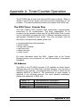
Appendix A. Timer/Counter Operation
The PCI-8554 has at most four interval 8254 chips on board. Refer to
chapter 2 and 4 for the signal connection and the configuration of the
counters. The following sections describe the details of the 8254 chip.
The 8254 Timer / Counter Chip
The Intel (Tundra) 8254 contains three independent, programmable,
multi-mode 16 bit counter/timers. The three independent 16 bit
counters can be clocked at rates from DC to 8MHz MHz. Each counter
can be individually programmed with 6 different operating modes by
appropriately formatted control words. The most commonly uses for
the 8254 in microprocessor based system are:
•
•
•
•
•
•
programmable baud rate generator
event counter
binary rate multiplier
real-time clock
digital one-shot
motor control
For more information about the 8254 , please refer to the Tundra
Microprocessors and peripherals or Intel Microsystems Components
Handbook.
I/O Address
The 8254 in the PCI-8554 occupies 4 I/O address as shown below.
Although there are four 8254 chips on board, however, only one chip is
selected in one moment. The programming of 8254 is control by the
registers BASE+0 to BASE+3. The functionality of each register is
specified in the following sections. For more detailed information,
please refer handbook of 8254 chip.
BASE + 0
BASE + 1
BASE + 2
BASE + 3
LSB OR MSB OF COUNTER 0
LSB OR MSB OF COUNTER 1
LSB OR MSB OF COUNTER 2
CONTROL BYTE
Appendix A • 41
Control Byte
Before loading or reading any of these individual counters, the control
byte (BASE+3) must be loaded first. The format of the control byte is :
Bit
•
7
SC1
6
SC0
5
RL1
4
RL0
3
M2
2
M1
1
M0
0
BCD
SC1 & SC0 - Select Counter ( Bit 7 & Bit 6)
SC1
SC0
COUNTER
0
0
Select Counter 0
0
1
Select Counter 1
1
0
Select Counter 2
1
1
ILLEGAL
• RL1 & RL0 - Select Read/Load operation ( Bit 5 & Bit 4)
RL1
0
0
1
1
RL0
0
1
0
1
OPERATION
COUNTER LATCH FOR STABLE READ
READ/LOAD LSB ONLY
READ/LOAD MSB ONLY
READ/LOAD LSB FIRST, THEN MSB
• M2, M1 & M0 - Select Operating Mode ( Bit 3, Bit 2, & Bit 1)
M2
0
0
x
x
1
1
M1
0
0
1
1
0
0
M0
0
1
0
1
0
1
MODE
0
1
2
3
4
5
• BCD - Select Binary/BCD Counting ( Bit 0)
0
1
Note
42 • Appendix A
16-BITS BINARY COUNTER
BINARY CODED DECIMAL (BCD) COUNTER (4
DIGITAL)
The count of the binary counter is from 0 up to
65,535 and the count of the BCD counter is from
0 up to 9,999
Mode Definitions
In 8254, six operating modes can be selected. they are :
•
•
•
•
•
•
Mode 0 : Interrupt on Terminal Count
Mode 1 : Programmable One-Shot.
Mode 2 : Rate Generator.
Mode 3 : Square Wave Rate Generator.
Mode 4 : Software Triggered Strobe.
Mode 5 : Hardware Triggered Strobe.
All detailed description of these six modes are written in Intel
Microsystem Components Handbook Volume II Peripherals.
Timer / Counter Applications
Please refer to Chapter 4.
Appendix • 43
Product Warranty / Service
Seller warrants that equipment furnished will be free form defects in material
and workmanship for a period of one year from the confirmed date of
purchase of the original buyer and that upon written notice of any such defect,
Seller will, at its option, repair or replace the defective item under the terms of
this warranty, subject to the provisions and specific exclusions listed herein.
This warranty shall not apply to equipment that has been previously repaired
or altered outside our plant in any way as to, in the judgment of the
manufacturer, affect its reliability. Nor will it apply if the equipment has been
used in a manner exceeding its specifications or if the serial number has been
removed.
Seller does not assume any liability for consequential damages as a result
from our products uses, and in any event our liability shall not exceed the
original selling price of the equipment.
The equipment warranty shall constitute the sole and exclusive remedy of any
Buyer of Seller equipment and the sole and exclusive liability of the Seller, its
successors or assigns, in connection with equipment purchased and in lieu of
all other warranties expressed implied or statutory, including, but not limited
to, any implied warranty of merchant ability or fitness and all other obligations
or liabilities of seller, its successors or assigns.
The equipment must be returned postage-prepaid. Package it securely and
insure it. You will be charged for parts and labor if you lack proof of date of
purchase, or if the warranty period is expired.
Product Warranty