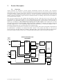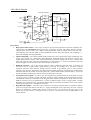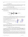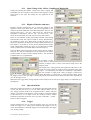
1
XZ030 AGILENT ACQIRIS USER MANUAL FAMILY OF ANALYZERS Models covered: AP235/AP240 with SSR AP235/AP240 with PeakTDC AP101/AP201 User Manual: Family of Analyzers ZM020040G RevD June 2007 The information in this document is subject to change without notice and may not be construed in any way as a commitment by Agilent Technologies Inc. While Agilent Technologies makes every effort to ensure the accuracy and contents of the document it assumes no responsibility for any errors that may appear. All software described in the document is furnished under license. The software may only be used and copied in accordance with the terms of license. Instrumentation firmware is thoroughly tested and thought to be functional but it is supplied “as is” with no warranty for specified performance. No responsibility is assumed for the use or the reliability of software, firmware or any equipment that is not supplied by Agilent Technologies Inc. or its affiliated companies. Any versions of this manual which are supplied with a purchased product will be replaced at your request with the latest revision in electronic format. At Agilent Technologies we appreciate and encourage customer input. If you have a suggestion related to the content of this manual or the presentation of information, please contact your local Acqiris representative or Acqiris Technical Support ([email protected]) or come visit our web site at http://www.acqiris.com. Trademarks: product and company names listed are trademarks or trade names of their respective companies Acqiris Headquarters: Acqiris USA: Acqiris Asia-Pacific: Agilent Technologies SA 12, chemin des Aulx CH-1228 Plan-les-Ouates Geneva Switzerland Agilent Technologies Inc. P.O. Box 2203 Monroe, NY 10949 USA Agilent Technologies Australia Pty Ltd 347 Burwood Highway, Forest Hill VIC 3131 Australia Tel: +41 22 884 32 90 Tel: 845 782 6544 Tel: +61 3 9210 2890 Fax: +41 22 884 32 99 Fax: 845 782 4745 Fax: +61 3 9210 5929 © Copyright Agilent Technologies Inc. June 2007 User Manual: Family of Analyzers Page 2 of 56 CONTENTS 1. OUT OF THE BOX ............................................................................................................................................. 6 1.1. 1.2. 1.3. 1.4. 1.5. 1.6. 1.7. 1.8. 1.9. 1.10. 1.11. 1.12. 1.13. 2. Message to the User ....................................................................................................................................... 6 Using this Manual .......................................................................................................................................... 6 Conventions Used in This Manual ................................................................................................................. 6 Disclaimer and Safety .................................................................................................................................... 6 Warning Regarding Medical Use................................................................................................................... 7 Packaging and Handling ................................................................................................................................ 7 Warranty......................................................................................................................................................... 7 Warranty and Repair Return Procedure, Assistance and Support .................................................................. 8 System Requirements..................................................................................................................................... 8 Transport & Shipping................................................................................................................................. 9 Maintenance ............................................................................................................................................... 9 Cleaning ..................................................................................................................................................... 9 Disposal and Recycling.............................................................................................................................. 9 INSTALLATION ............................................................................................................................................... 10 2.1. Installing the Software under Windows ....................................................................................................... 10 2.1.1. Warnings .............................................................................................................................................. 10 2.1.2. Multiple Versions................................................................................................................................. 10 2.1.3. Installation............................................................................................................................................ 10 2.2. Installing the Software for Linux ................................................................................................................. 20 2.2.1. Kernel Mode Driver Compilation ........................................................................................................ 21 2.2.2. Special cases......................................................................................................................................... 22 2.2.3. Environment variables for the Firmware.............................................................................................. 22 2.3. Installing the Hardware ................................................................................................................................ 22 2.4. After Restarting............................................................................................................................................ 23 2.4.1. Windows 2000 ..................................................................................................................................... 23 2.4.2. Windows XP ........................................................................................................................................ 23 2.5. LabVIEW RT............................................................................................................................................... 25 2.6. Installing the IVI-COM/C Driver................................................................................................................. 25 2.7. Distribution for Windows 2000/XP and Linux ............................................................................................ 26 3. PRODUCT DESCRIPTION ............................................................................................................................. 27 3.1. Overview...................................................................................................................................................... 27 3.2. Channel Input............................................................................................................................................... 29 3.2.1. Coupling & Impedance ........................................................................................................................ 29 3.2.2. Input Protection.................................................................................................................................... 29 3.2.3. Mezzanine Front-end............................................................................................................................ 29 3.2.4. Bandwidth and Rise Time .................................................................................................................... 29 3.2.5. Input Voltage and Offset ...................................................................................................................... 29 3.2.6. Vertical Resolution............................................................................................................................... 30 3.2.7. DC Accuracy........................................................................................................................................ 30 3.3. Trigger.......................................................................................................................................................... 30 3.3.1. Trigger Source...................................................................................................................................... 30 3.3.2. Trigger Coupling.................................................................................................................................. 30 3.3.3. Trigger Level........................................................................................................................................ 30 3.3.4. Trigger Slope........................................................................................................................................ 31 3.3.5. External Trigger Output ....................................................................................................................... 31 3.3.6. Trigger Status ....................................................................................................................................... 31 3.3.7. Trigger Veto and Timeout (AP101/AP201 ONLY) ............................................................................. 31 3.4. Data Acquisition – Common........................................................................................................................ 32 3.4.1. Timing.................................................................................................................................................. 32 3.4.2. Sampling Rate ...................................................................................................................................... 32 3.5. Data Acquisition - Digitizer Mode............................................................................................................... 32 3.5.1. Acquisition Memory and Time Base Range - Digitizer Mode............................................................. 32 User Manual: Family of Analyzers Page 3 of 56 3.5.2. Pre- and Post-Trigger Delay - Digitizer Mode ..................................................................................... 32 3.5.3. Single and Sequence Acquisitions - Digitizer Mode............................................................................ 33 3.6. Data Acquisition – Analyzer mode .............................................................................................................. 33 3.6.1. Random and Synchronized Triggers .................................................................................................... 35 3.6.2. Time Base Range ................................................................................................................................. 35 3.6.3. Dual-Bank Memory & Buffered Sequence Acquisition....................................................................... 35 3.6.4. Buffered Acquisition Mode with Data Readout ................................................................................... 36 3.7. AP235/AP240 Data processing.................................................................................................................... 36 3.7.1. User Gates ............................................................................................................................................ 36 3.7.2. Threshold gates .................................................................................................................................... 36 3.7.3. Time stamp information ....................................................................................................................... 37 3.7.4. Peak detection ...................................................................................................................................... 37 3.7.5. Interpolation of Peak Position and Amplitude ..................................................................................... 37 3.7.6. Histogramming Peak Data ................................................................................................................... 37 3.8. AP101/AP201 Data processing.................................................................................................................... 38 3.8.1. User Gates ............................................................................................................................................ 38 3.8.2. Simple peak detection .......................................................................................................................... 38 3.8.3. Peak detection with Hysteresis............................................................................................................. 38 3.8.4. Peak Interpolation ................................................................................................................................ 38 3.9. External Clock and Reference...................................................................................................................... 39 3.10. Front Panel Inputs and Controls............................................................................................................... 39 3.11. Internal Calibration .................................................................................................................................. 39 3.12. Electrical, Environmental and Physical Specifications ............................................................................ 40 3.12.1. Electrical .............................................................................................................................................. 40 3.12.2. Environmental and Physical................................................................................................................. 40 4. RUNNING THE AP_SSRDEMO APPLICATION ........................................................................................ 41 4.1. Getting Started with AP_SSRDemo ............................................................................................................ 41 4.2. Editing Fields ............................................................................................................................................... 42 4.3. Digitizer Control Panel and Functions ......................................................................................................... 42 4.3.1. Input Voltage Scale, Offset, Coupling and Bandwidth ........................................................................ 43 4.3.2. Digitizer Timebase and more ............................................................................................................... 43 4.3.3. Operation Mode ................................................................................................................................... 43 4.3.4. Trigger.................................................................................................................................................. 43 4.3.5. External Clock...................................................................................................................................... 44 4.3.6. Control IO Settings .............................................................................................................................. 44 4.3.7. Acquisition Mode................................................................................................................................. 44 4.3.8. Display options..................................................................................................................................... 44 4.4. Analyzer Control Panel and Functions......................................................................................................... 44 4.4.1. Analyzer Timebase and Memory ......................................................................................................... 45 4.4.2. User Gate definition ............................................................................................................................. 45 4.4.3. Threshold Gate definition..................................................................................................................... 45 4.4.4. PeakTDC mode - Peak and Histogram definition ................................................................................... 45 4.4.5. Additional Controls & Time Stamp data.............................................................................................. 46 4.4.6. Waveform storage ................................................................................................................................ 46 4.4.7. Control panel reactivation .................................................................................................................... 46 4.4.8. Temperature display............................................................................................................................. 47 4.4.9. Zoom display control ........................................................................................................................... 47 5. RUNNING THE APX01DEMO APPLICATION........................................................................................... 48 5.1. Getting Started with APx01Demo................................................................................................................ 48 5.2. Editing Fields ............................................................................................................................................... 49 5.3. Digitizer Control Panel and Functions ......................................................................................................... 49 5.3.1. Input Voltage Scale, Offset, Coupling and Bandwidth ........................................................................ 50 5.3.2. Digitizer Timebase and more ............................................................................................................... 50 5.3.3. Trigger.................................................................................................................................................. 51 5.3.4. Acquisition Mode................................................................................................................................. 51 5.3.5. Persistence display ............................................................................................................................... 52 5.4. Analyzer Control Panel and Functions......................................................................................................... 52 User Manual: Family of Analyzers Page 4 of 56 5.4.1. Analyzer Timebase and Memory ......................................................................................................... 52 5.4.2. Gate definition...................................................................................................................................... 52 5.4.3. Trigger Veto and Timeout.................................................................................................................... 52 5.4.4. Hysteresis Mode Peak Parameters ....................................................................................................... 53 5.4.5. Display of Peaks................................................................................................................................... 53 5.5. Display Window Functions.......................................................................................................................... 53 5.5.1. Waveform storage ................................................................................................................................ 53 5.5.2. Control panel reactivation .................................................................................................................... 53 5.5.3. Temperature display............................................................................................................................. 54 5.5.4. Zoom display control ........................................................................................................................... 54 6. APPENDIX A: XA100 BNC INPUT OVERVOLTAGE PROTECTION .................................................... 55 7. APPENDIX B: XP102 FAN UNIT FOR THE AP FAMILY OF MODULES .............................................. 56 User Manual: Family of Analyzers Page 5 of 56 1. Out of the Box 1.1. Message to the User Congratulations on having purchased an Agilent Technologies Acqiris data conversion product. Acqiris Digitizers/Analyzers are high-speed data acquisition modules designed for capturing high frequency electronic signals. To get the most out of the products we recommend that you read this manual carefully. We trust the product you have purchased will meet with your expectations and provide you with a high quality solution to your data conversion applications. 1.2. Using this Manual This guide assumes you are familiar with the operation of a personal computer (PC) running a Windows 2000/XP or other supported operating system. It also assumes you have a basic understanding of the principles of data acquisition using either a waveform digitizer or a digital oscilloscope. The manual is divided into 5 separate sections. To understand the elements of operation for the module it is essential that you read them as appropriate. Chapter 1 OUT OF THE BOX, describes what to do when you first receive your new Acqiris product. Special attention should be paid to sections on safety, packaging and product handling. Before installing your product please ensure that your system configuration matches or exceeds the requirements specified. Chapter 2 INSTALLATION, covers all elements of installation and performance verification. Before attempting to use your Acqiris product for actual measurements we strongly recommend that you read all sections of this chapter. Chapter 3 PRODUCT DESCRIPTION, provides a full description of all the functional elements of the Analyzer. Chapter 4 RUNNING THE AP_SSRDEMO APPLICATION, describes the operation of an application that enables basic operation of Acqiris AP235/AP240 digitizers and analyzers in a Windows 2000/XP environment. Chapter 5 RUNNING THE APX01DEMO APPLICATION, describes the operation of an application that enables basic operation of Acqiris AP101/AP201 digitizers and analyzers in a Windows 2000/XP environment For information necessary for writing you own software to control Acqiris products you should refer to the Programmer’s Guide and the Programmer’s Reference Manual. 1.3. Conventions Used in This Manual The following conventions are used in this manual: This icon to the left of text warns that an important point must be observed. WARNING Denotes a warning, which advises you of precautions to take to avoid being electrically shocked. CAUTION Denotes a caution, which advises you of precautions to take to avoid electrical, mechanical, or operational damages. NOTE Denotes a note, which alerts you to important information. Italic text denotes a warning, caution, or note. Bold Italic text is used to emphasize an important point in the text or a note mono text is used for sections of code, programming examples and operating system commands. 1.4. Disclaimer and Safety The AP Series PCI Analyzer cards have been designed to operate in a standard PCI slot found inside most personal computers. Power for the modules is provided by plugging them into a free slot (refer to the installation procedure). CAUTION: Do not exceed the maximum input voltage rating! The maximum input voltage for 50 Ω input impedance is ±5 V. User Manual: Family of Analyzers Page 6 of 56 1.5. Warning Regarding Medical Use The AP Series PCI Analyzer cards are not designed with components and testing intended to ensure a level of reliability suitable for use in treatment and diagnosis of humans. Applications of these cards involving medical or clinical treatment can create a potential for accidental injury caused by product failure, or by errors on the part of the user. These cards are not intended to be a substitute for any form of established process or equipment used to monitor or safeguard human health and safety in medical treatment. WARNING: The modules discussed in this manual have not been designed for making direct measurements on the human body. Users who connect an Acqiris module to a human body do so at their own risk. 1.6. Packaging and Handling Your Analyzer is shipped with the following components: • A small 3.5” compact disc in an Acqiris paper CD envelope that includes o 10 product user manuals in electronic form (Signal Analyzers, Streamer Analyzers, Family of 8-bit Digitizers, Family of 10-bit Digitizers, Family of 12-bit Digitizers, Family of Averagers, Family of Analyzers, Family of Time Counters, CC10X Family of CompactPCI Crates and CC121 CompactPCI Crate), o 1 Programmer’s Guide and 1 Programmer’s Reference Manual, o device drivers with sample software for different operating systems, environments and languages, o the AcqirisAnalyzers application, a demonstration program for the AC/SC Analyzer products, o the AcqirisLive application, a demonstration program for our digitizer and averager products, o the DemoSSR application, a demonstration program for the Acqiris AP235/AP240 Analyzers, o the DemoAPX01 application, a demonstration program for the Acqiris AP101/AP201 Analyzers, o the DemoTC application, a demonstration program for the Acqiris TC840/TC890 Time Counters, o product data sheets, o full installation procedures for use with Microsoft Windows, National Instruments LabVIEW RT, Wind River VxWorks, IVI-COM/C, and Linux software. • A declaration of conformity • Optional documentation such as a model-dependent document giving Specifications & Characteristics, a Calibration Certificate, or a Performance Verification After carefully unpacking all items, inspect each to ensure there are no signs of visible damage. Also check that all the components received match those listed on the enclosed packing list. Agilent Technologies cannot accept responsibility for missing items unless we are notified promptly of any discrepancies. If any items are found to be missing or are received in a damaged condition please contact the Customer Support Center or your local supplier immediately. Retain the box and packing materials for possible inspection and/or reshipment. 1.7. Warranty All Agilent Technologies Acqiris Digitizer products are warranted to operate within specification, assuming normal operation, for a period of three years from the date of shipment. It is recommended that yearly calibration be made in order to verify product performance. All repairs, replacement and spare parts are warranted for a period of 3 months. A 5-year repair warranty is available as an option. Agilent Technologies endeavors to provide leading edge technology that includes the latest concepts in hardware and software design. As such software and firmware used with the products is under continual refinement and improvement. All software and instrument firmware is supplied “as is” with no warranty of any kind. Software and firmware is thoroughly tested and thought to be functional at the time of shipment. At Agilent Technologies’ discretion software and firmware may be revised if a significant operational malfunction is detected. Products supplied but not manufactured by Agilent Technologies are covered solely by the warranty of the original equipment manufacturer. In exercising this warranty, Agilent Technologies will repair or replace any product returned to the Agilent service center, within the warranty period. The warranty covers all defects that are a result of workmanship or materials. This excludes defects that are caused by accident, misuse, neglect, or abnormal operation. User Manual: Family of Analyzers Page 7 of 56 The purchaser is responsible for returning the goods to the nearest Agilent service center. This includes transportation costs and insurance. Agilent Technologies will return all warranty repairs with transportation prepaid. 1.8. Warranty and Repair Return Procedure, Assistance and Support Agilent Technologies Inc. acquired Acqiris SA and its product lines in December 2006. Before returning any Agilent Technologies Acqiris product for repair please contact your nearest Agilent Technologies Service Center. You can find information about technical and professional services, product support, and equipment repair and service on the Web, see http://www.agilent.com/find/service (or http://www.agilent.com/ and after selecting your country click on Contact Us). The service center will ask for your name, company, phone number and address, the model and serial numbers of the unit to be repaired, and a brief description of the problem. Before issuing a Service Order they will ask you to communicate with us by phone or eMail so that we can learn as much as needed about the problems observed. If a unit returned under guarantee is found to be working normally and this procedure was not followed we reserve the right to charge you for the work done. For your nearest customer support center contact Acqiris at 1-877-ACQIRIS in the USA, +41 22 884 32 90 in Europe or +61 3 9210 2890 in the Asia-Pacific region. Alternatively, please contact Acqiris Technical Support ([email protected]) or come visit our web site at http://www.acqiris.com. The Agilent Technologies Support Centers can also help redirect you for any questions concerning the installation and operation of your equipment. 1.9. System Requirements In order to obtain reasonable performance from your digitizer, Acqiris products need the following minimum PC System Requirements: Processor: 150 MHz Pentium (higher recommended) Memory: 64 Mbytes RAM. The previous number is a very rough estimate. Assuming that you are using AcqirisLive or an application of your own that operates on the acquired data it seems reasonable to ask for 10 times the total acquisition memory that you will be using at the same time in the application. Performance is likely to be degraded if less memory is available. Display resolution: At least 800 x 600 pixels and 256 colors for use of AcqirisDemo programs. Operating System: Microsoft Windows 2000/XP including 2003 Server, Wind River VxWorks 5.5.1, and Linux. The following Linux versions have compiled loadable kernel modules: RedHat Enterprise Linux Version 3 - Kernel Version 2.4.21-4.EL RedHat Enterprise Linux Version 3 - Kernel Version 2.4.21-4.ELsmp, Suse Linux 9.2 - Kernel version 2.6.8-24-smp, Debian Sarge 3.1 2.6.8-3-686, Debian 4.0 etch Kernel version 2.6.18-4-686, Scientific Linux 4.4 Kernel version 2.6.9-11.EL). Linux kernel driver source code is available for compilation. Support for Windows 95/98/NT4 is included “as is” since these operating systems are no longer supported by Microsoft. Hard Drive Space: 20 Mbytes Minimum CD Drive (or any method to copy Acqiris Software installation files from CD to the hard drive such as LAN, floppy drive, etc.) LabVIEW: The Acqiris LabVIEW driver is available for National Instruments LabVIEW versions 7.1or 8.0 LabVIEW RT: The Acqiris LabVIEW RT driver is available for National Instruments LabVIEW RT version 7.1 or higher. The VISA driver must be version 3.0 or higher. MATLAB: The Acqiris MEX interface can be used with MathWorks MATLAB 6.5 or a newer vesion. Visual BASIC: The interface files and examples are available for Microsoft Visual Basic versions 5 or 6 and the interface files only for .NET. Tornado: The example files are useable with Wind River Tornado 2.2.1 User Manual: Family of Analyzers Page 8 of 56 1.10. Transport & Shipping CAUTION: Cards can be safely transported in their original shipping packages. DC cards can be transported when properly mounted in a CompactPCI crate. The transport of DP cards mounted in a PC is a more delicate issue. Because of their mass the cards can vibrate loose unless they are properly secured and braced. DP cards held only in the front and on the bottom should not be shipped in their PC. However, properly mounted DP cards with XP103 or XP105 fans can be sufficiently well held; the Adjustable retainer must be used so as to hold the card in place. To package the instrument for shipping: Step Notes 1. Place the instrument in its original packaging materials. • If the original packaging materials are not available, use a professional packaging service. Contact your Agilent Service Center for more information. 2. Surround the instrument with at least 3 to 4 inches (8 to 10 cm) of its original packing material or bubble-pack to prevent the instrument from moving in its shipping container. 3. After wrapping it with packing material, place the instrument in its original shipping container or a strong shipping container that is made of double-walled corrugated cardboard with 159 kg (350 lb) bursting strength. • The shipping container must be large and strong enough to accommodate your instrument and allow at least 3 to 4 inches (8 to 10 cm) on all sides for packing material. 4. Seal the shipping container securely with strong nylon adhesive tape. 5. Mark the shipping container “FRAGILE, HANDLE WITH CARE” to help ensure careful handling. 6. Use the address obtained from your Agilent Technologies Service Center. 7. Retain copies of all shipping papers. CAUTION: Damage can result if the original packaging materials are not used. Packaging materials should be anti-static and cushion the instrument on all sides. NEVER USE STYRENE PELLETS IN ANY SHAPE AS PACKAGING MATERIALS. They do not adequately cushion the instrument or prevent it from moving in the shipping container. Styrene pellets can also cause equipment damage by generating static electricity or by lodging in fan motors. 1.11. Maintenance The cards do not require any maintenance. There are no user serviceable parts inside. A periodic calibration can be obtained on request. 1.12. Cleaning Cleaning procedures consist only of exterior cleaning. Clean the exterior surfaces of the module with a dry lint-free cloth or a soft-bristle brush. If any dirt remains, wipe with a cloth moistened in a mild soap solution. Remove any soap residue by wiping with a cloth moistened with clear water. Do not use abrasive compounds on any parts. 1.13. Disposal and Recycling Electronic equipment should be properly disposed of. Acqiris Analysers/Digitizers and their accessories must not be thrown out as normal waste. Separate collection is appropriate and may be required by law. User Manual: Family of Analyzers Page 9 of 56 2. Installation This chapter describes how to install the Acqiris hardware and software for Windows 2000/XP, National Instruments LabVIEW RT, Linux, or Wind River VxWorks. NOTE: For a first time installation we strongly recommend installing the software before inserting the hardware into the PC. 2.1. Installing the Software under Windows 2.1.1. Warnings If Setup detects a previous installation of Acqiris software on your system, a warning screen will be displayed. It is recommended to exit Setup and uninstall older versions. The installer from software releases prior to Acqiris Software 2.0 installed the Digitizer Driver DLL files into the System directory. These will be removed by Setup. If you wish to keep the old installation on your system, you should exit Setup, and move all Acqiris driver files (acqiris*, acqrs* and acqir*) to some archive directory. The DLL files will be installed into the bin subdirectory of the Acqiris software root, and the corresponding path will be added to the PATH environment variable. 2.1.2. Multiple Versions With the software installation from Acqiris Software 2.0 (or above), it is possible to keep multiple versions on the same system, but you must specify a different root directory (i.e. Install Folder). If you keep the same directory, Setup will overwrite your previous installation. To go back to a previous version, you must change the PATH environment variable and reinstall the Kernel driver. Under Windows 2000/XP: 1. Copy the SYS file from <old_AcqirisSoftware_root>\bin\kernel to the Windows\System32\drivers directory. 2. Change the AcqirisDxRoot, AcqirisDxDir and PATH environment variables to the old root. 3. Reboot the computer. 2.1.3. Installation Before installing the Acqiris hardware, you should complete the following steps to install the software for Windows 2000/XP. NOTE: You will need administrator privileges to complete the software installation under Windows 2000/XP. 1. Insert the Acqiris Software CD into the CD-ROM drive of your computer. If the Autorun program does not start automatically (Autoplay disabled), you can start it manually, or navigate to the AcqirisSoftware\Windows folder in order to display the files included. 2. Choose Install AcqirisSoftware for Windows 2000/XP (or run Setup.exe from AcqirisSoftware\Windows folder). After several seconds for initialization the following screen will appear. User Manual: Family of Analyzers Page 10 of 56 the 3. To proceed with the installation click “Next”. The following screen will be shown. 4. Please enter your user information and click “Next” to continue. If the program finds that there is still Acqiris software installed on your machine a warning panel (not shown) will appear. Otherwise, the next screen shows: User Manual: Family of Analyzers Page 11 of 56 5. Pick the desired combination of module families and click "Next" to continue. 5. The screen above will normally allow the documentation to be installed. Remove the check from the box if you do not want online access to the manuals. 6. The next screen allows you to enable LabVIEW RT and/or Wind River VxWorks support. By default there will be none but if desired you can install any of them together with Windows support or without Windows support. Click “Next” to continue. User Manual: Family of Analyzers Page 12 of 56 7. The screen below asks for the desired installation type. After having made your choice Click “Next” to continue. 8. If you chose the Custom installation, the following screen will let you select each package individually. Note that the space indicated for LabVIEW, Firmware and UserManual packages is incorrect. The correct values are 4.1 MB, 21 MB, and 27 MB respectively. User Manual: Family of Analyzers Page 13 of 56 9. If MATLAB is installed on your machine, you will be asked to point the installer to the MATLAB root directory. You should do this if you want the installer to modify the standard startup.m file to incorporate the Acqiris adaptor. 10. Now that the elements of the installation have all been decided you will be prompted for the installation folder. This will be the root directory of the Acqiris software installation. If User Manuals (27 MB) and Firmware (21 MB) are loaded more space than indicated here will be required on the drive. For the case of a Tornado 2.2 installation the folder name should not contain any spaces. 11. Furthermore, you should give a name to the shortcut folder. This is the menu entry under Start → Programs where you will find the shortcuts for AcqirisLive, manual(s), etc. User Manual: Family of Analyzers Page 14 of 56 12. If you have enabled the installation of 12-bit Digitizers, Averagers, or Analyzers, the next screen lets you change the name of the directory where the FPGA firmware will be installed. 13. AcqirisLive needs the LabWindows/CVI 7.0 Run-Time Engine to run. If Setup has detected that a LabWindows/CVI Run-Time Engine is already installed on your system, it will ask you if you would like to install it locally for AcqirisLive anyway. If you are not sure about the version of the CVI Run-Time Engine on your system, it is recommended to install it locally. Click “Next” to continue. User Manual: Family of Analyzers Page 15 of 56 14. Depending on the install type, you may be asked which LabVIEW version format you want for the LabVIEW files. Select the appropriate format and click “Next” to continue. 15. A summary will be shown to allow you to check what you have asked for User Manual: Family of Analyzers Page 16 of 56 16. You are now ready to install. You may still go back to any previous screen to modify your selection. Click “Install” when ready. 17. Setup will now copy the files and make the necessary changes to your system. When done, an information screen will be displayed. Please read this carefully. User Manual: Family of Analyzers Page 17 of 56 18. Registration of your installation will help us provide you with better support. You will also be notified of updates and upgrades. All information submitted to us will be treated confidentially and never be disclosed outside the company. User Manual: Family of Analyzers Page 18 of 56 19. Setup will prepare a registration e-mail in your e-mail client application upon termination of the setup procedure. You can then decide whether or not you wish to send it. You may also add comments. Uncheck the box if you do not want to register your installation. 20. Click “Finish”. The software installation is now complete. 21. You can now either accept the suggestion to restart the computer or you should shutdown your computer and proceed with the hardware installation. User Manual: Family of Analyzers Page 19 of 56 2.2. Installing the Software for Linux The Acqiris Software is ready to install and run on Linux systems with any of the following: RedHat Enterprise Linux Version 3 - Kernel Version 2.4.21-4.EL RedHat Enterprise Linux Version 3 - Kernel Version 2.4.21-4.ELsmp, Suse Linux 9.2 - Kernel version 2.6.8-24-smp, Debian Sarge 3.1 2.6.8-3-686, Debian 4.0 etch Kernel version 2.6.18-4-686, Scientific Linux 4.4 Kernel version 2.6.9-11.EL) The following tar files exist with the driver and library compiled with the GNU gcc version shown: AcqirisLinux-3.1a-gcc-3.3.tar.gz - compiled under Suse 9.2 with GNU gcc 3.3. AcqirisLinux-3.1a-gcc-3.4.tar.gz - compiled under SL 4.4 with GNU gcc 3.4. AcqirisLinux-3.1a-gcc-4.1.tar.gz - compiled under Debian etch with GNU gcc 4.1. The Kernel Driver source code is available for recompilation for users with other Linux systems. The appropriate tar file should be copied to a local directory (e.g. your home directory) and then unpacked by using the following command tar xzf AcqirisLinux-3.1a-gcc-X.x.tar.gz The resulting directory AcqirisLinux contains an install script drv-install and a graphical Demo program demo/AcqirisDemo. Before installing the driver you have to put the correct version of the Kernel mode driver into acqirisPCI.o. Type cd AcqirisLinux/lib/modules and either cp acqrsPCI.o[.n] acqrsPCI.o (Linux kernel 2.4) or cp acqrsPCI.ko[.n] acqrsPCI.ko (Linux kernel 2.6) where [.n] is the running version of the Linux kernel. This can be obtained by running the command uname -r The following versions exist: acqrsPCI.o.2.4.21-4.EL User Manual: Family of Analyzers for Red Hat Enterprise Linux version 3 Page 20 of 56 acqrsPCI.ko.2.6.8-3-686 acqrsPCI.ko.2.6.8-24-smp acqrsPCI.ko.2.6.9-11.EL acqrsPCI.ko.2.6.18-4-686 for Debian 3.1 'sarge' for Suse 9.2 for Scientific Linux 4.4 for Debian 4.0 'etch' To install the driver and the load script to the system, you have to get super user privileges and execute the driver install script by typing, cd AcqirisLinux ./drv-install add You can check that the driver is loaded properly with lsmod or dmesg. The drv-install script has the following additional functionality: drv-install rem to remove the driver and load script drv-install res to restart the driver If you intend to use an Averager, an Analyzer, or a 12-Bit Digitizer you must install the Firmware .bit files. You can either copy them from the Firmware directory of the CD-ROM or download them from our WEB site. They should be placed in the Firmware subdirectory of AcqirisLinux. In the case of the CD-ROM, this can be done by continuing the above command sequence with the following: cp /mnt/CDRom/Firmware/*.bit Firmware/ 2.2.1. Kernel Mode Driver Compilation For some special kernels, for example SMP, the kernel mode driver will have to be recompiled on the target system. All files needed to compile a new kernel mode driver are in AcqirisLinux/linuxdriverpci for Kernel 2.4 or in AcqirisLinux/linux2.6driverpci for Kernel 2.6 The makefile can be used for compilation under a standard compatible distribution. To compile the driver, the kernel header files need to be installed. Furthermore, depending on the Linux distribution, the kernel source files may need to be installed. The makefile will try to guess where they are located. If it fails, see instructions inside the makefile itself to specify manually where these kernel header files are located. To compile a new kernel under linux-2.4, issue the following commands: cd linuxdriverpci make clean to remove all *.o files in AcqirisLinux/linuxdriverpci. make to generate a new kernel mode driver acqrsPCI.o and also copy it to the directory AcqirisLinux/lib/modules where the install script (drv_install) can access it. drv_install rem to remove the previous installed kernel mode driver. drv_install add to install the new driver. To compile a new kernel under linux-2.6, issue the following commands: cd linux2.6driverpci make clean all to generate a new kernel mode driver acqrsPCI.ko from scratch. make install to copy the kernel module where it should reside. Note that this version of the loadable kernel module had been tested on Linux kernel versions up to 2.6.18. However, starting with kernel 2.6.17, a few kernel functions relating to the device classes are no longer available to proprietary modules. Thus automatic creation of the /dev/acqrsPCI node has to be done manually in the /etc/rc.local file. For Debian users, in order to compile the kernel module on a system, a few packages that match the current kernelimage must be installed. For instance, on a Debian 3.1 sarge system 686 the required packages are: kernel-image-2.6-686 kernel-image-2.6.8-3-686 kernel-headers-2.6-686 kernel-headers-2.6.8-3 kernel-headers-2.6.8-3-686 kernel-kbuild-2.6-3 User Manual: Family of Analyzers Page 21 of 56 2.2.2. Special cases If you are running a Linux distribution that doesn’t use the standard paths for the load scripts, you can load the driver with the command cd AcqirisLinux ./drv-install load Copy the driver to the module directory as follows: cp lib/modules/acqrsPCI.o[.n] /lib/modules/{kv}/ACQIRIS/acqrsPCI.o where [.n] is the optional designation of the desired version of the acqrsPCI driver as given above and {kv} is the appropriate system kernel version (obtained with uname -r, i.e. 2.4.20). Then add the following command to /etc/rc.local. /sbin/insmod –f /lib/modules//{kv}/ACQIRIS/acqrsPCI.o For systems using udev (the dynamic /dev/ hierarchy) it may be convenient to automatically create the /dev/acqrsPCI node at boot. To do this, add the following command to the /etc/rc.local file: /sbin/mknod -m 666 /dev/acqrsPCI c 124 0 2.2.3. Environment variables for the Firmware Automatic loading of the firmware needed by 12-bit, analyzer, and averager modules relies on the environment variable AcqirisDxDir pointing to the directory containing the file AqDrv4.ini which in turn points to the directory containing the Firmware .bit files. Therefore, assuming that your Firmware is in /usr/local/AcqirisLinux/Firmware and that AqDrv4.ini is in /usr/local/AcqirisLinux/demo then you must edit AqDrv4.ini so that it contains the line fpgaPath=/usr/local/AcqirisLinux/Firmware Then, if your shell is csh or tcsh modify the /etc/csh.login file to contain the line setenv AcqirisDxDir /usr/local/AcqirisLinux/demo or, if your shell is bash, ksh, zsh or sh, modify the /etc/profile file to contain the lines AcqirisDxDir=/usr/local/AcqirisLinux/demo export AcqirisDxDir 2.3. 1. Installing the Hardware Turn off the power of the PC and the crate in the case of a CompactPCI module. CAUTION: For PCI modules the PC may have to be unplugged to ensure that the PCI bus has no power available. However, CompactPCI crates can be left plugged in since this ensures proper grounding. CAUTION: Touch the antistatic package to a grounded object before removing the card from the package. Electrostatic discharge can damage the card. 2. Open the PC, identify a free PCI slot and carefully insert the DP Series card into it. Be sure to ground yourself by touching the grounded PC frame and avoid touching any components on the DP Series card. Make sure that the grounding of the card’s mounting bracket to the back panel rail of the computer is done correctly. If present make sure that the fan's adjustable retainer is correctly positioned and tightened for mechanical support. Close the PC. 3. Turn on the power of the PC and start the operating system. NOTE: Acqiris Digitizers are equipped with a LED. If this LED is not glowing orange or red when the power is applied there is a severe problem. Either the module is broken or the necessary voltages for its use are not available. Devices that were installed using a previous version of Acqiris Software the instruments in these logical positions will still appear as Unknown Devices. This can be changed to the new Acqiris type category with the Grey Diamond icon by Uninstalling the device and then Installing again. Instructions on this procedure can be found in the ReadMe.txt file in the manuals folder of your Acqiris Software installation. User Manual: Family of Analyzers Page 22 of 56 2.4. After Restarting 2.4.1. Windows 2000 Under Windows 2000, you must login with administrator privileges after the first boot following the hardware installation; the Plug&Play system must have the appropriate privileges to be able to complete your hardware installation successfully. After a successful hardware installation, you will be able to use your Acqiris Digitizer(s) with normal privileges. At the first boot following the hardware installation, Windows will detect the new hardware and will install the devices automatically. The following image will appear. NOTE: In some systems an application program (such as AcqirisLive) will not yet work correctly at this point. One additional boot cycle may be needed if this is the first time that a hardware board is being installed. 2.4.2. Windows XP Under Windows XP, you must login with administrator privileges after the first boot following the hardware installation; the Plug&Play system must have the appropriate privileges to be able to complete your hardware installation successfully. After a successful hardware installation, you will be able to use your Acqiris Digitizer(s) with normal privileges. If you login with administrator privileges after the first boot following the hardware installation, Windows will detect the new hardware and start the “Found New Hardware Wizard” after a few seconds. To proceed with the installation click "No, not this time" and then “Next”. The following window will appear: User Manual: Family of Analyzers Page 23 of 56 To proceed with the installation click “Next”. You should then see and then User Manual: Family of Analyzers Page 24 of 56 NOTE: In some systems an application program (such as AcqirisLive) will not yet work correctly at this point. One additional boot cycle may be needed if this is the first time that a hardware board is being installed. 2.5. LabVIEW RT During program development you can choose whether you use LabVIEW or LabVIEW RT compatible libraries by switching the version present in National Instruments\LabVIEW m.n\instr.lib\. This swap can be facilitated by using the Install VI library for LabVIEW or LabVIEW Real-Time shortcut available in the Shortcut folder under Start → Programs. There is only one Acqiris Driver. It supports all Acqiris Instruments. The instructions below concern LabVIEW RT as used in NI PXI processors. The Aq_RT.inf and AqRT_4.ini files must be uploaded to the target. To do this, • start the MAX application, • right click on the target • select file transfer • select the Aq_RT.inf file on your host machine and upload ('To Remote') to the LabVIEW RT working directory (/NI-RT/system) on the target • select the Aq_RT.ini file on your host machine and upload ('To Remote') to the LabVIEW RT working directory (/NI-RT/system) giving it the name AqDrv4.ini For Acqiris modules which need FPGA files you should, • create the folder \firmware in the /NI-RT/system directory using the file transfer application • select the FPGA files (from <AcqirisDxRoot>\Firmware) you want to copy to the target and upload them into the firmware directory Restart the target after finishing the file transfers. Restart the MAX Explorer and you should have Acqiris digitizers detected in your PXI system. 2.6. Installing the IVI-COM/C Driver Please install Acqiris Software for Windows first. Then the Acqiris Software CD Autorun program gives access to two installers: IVI Shared Components 1.4 User Manual: Family of Analyzers Page 25 of 56 IVI-COM/C IviAqD1 driver These must be installed in the order shown above. For more information you can then consult the Readme.txt file in the IVI\Drivers\IviAqD1 folder or the documentation through the program shortcut present under Ivi/IviAqD1. 2.7. Distribution for Windows 2000/XP and Linux The manuals/ReadMe.txt file contains a list of files to be found after a complete installation of Acqiris Software on Windows systems. Similarly the ReadMeLinux file gives the list of files corresponding to that installation. User Manual: Family of Analyzers Page 26 of 56 3. Product Description 3.1. Overview Acqiris Analyzers are designed to provide superior measurement precision and accuracy. Key acquisition specifications (such as DC accuracy, integral and differential non-linearity) have been optimized to deliver maximum measurement fidelity. Careful circuit layout, custom IC’s and special packaging techniques have all been employed to reduce the overall random and correlated system noise. The use of custom IC’s also dramatically reduces the total number of discrete components required. This has tremendous benefits on reliability and also allows the modules to use a minimal amount of power. The AP series Analyzers are PCI modules that plug directly into any vacant PCI slot in a PC. They are fully programmable over the PCI bus and deliver 2 GS/s (AP240/AP201) and 1 GS/s (AP235/AP101) buffered acquisition performance. An acquired data sequence can be processed and transferred to a host processor over the PCI bus at speeds up to 100 Mbytes/s, while simultaneously acquiring the next data sequence. This explains the use of the term Sustained Sequential Recording (SSR). When appropriately configured, an Analyzer can reliably acquire all incoming triggers up to a rate considerably higher than that achievable by a conventional digitizer. This is particularly useful for the case of constant trigger rates in the kHz range. For complete technical specifications concerning your particular analyzer please refer to the product’s Specifications & Characteristics. In addition, we maintain up-to-date versions of all product data sheets on our web site (www.acqiris.com). The data sheets are available in pdf format and are best viewed using Adobe Acrobat software. If you have trouble accessing our web site, or viewing the data sheets, please contact your nearest sales office. A P235/AP240 BLO CK D IAGRA M Front Panel Signals CH1 Dual C hannel M ezzanine C H1 CH 2 C ross Point Sw itch ADC 1 1 G S/s 8-bit M AC 1 D em ux & M em ory Processing Block C H2 Offset and G ain C ontrol Ditherer 8-bit DAC ADC 2 M U LTI_IO 1 G S/s 8-bit EXT M AC 2 2xFPGA XC2V 3000 24x m em ory D em ux & M em ory CKin Trig Out I/O A CO S M ezzanine C PLD Trigger C ircuit I/O B Synchronizer P1 P2 Internal Reference Clock Clock Synch & Start PLX PCI Interface 100 M B/s PC I B us User Manual: Family of Analyzers Page 27 of 56 AP201 Block Diagram AP201 Block Diagram 8 bits 1GS/S 50 Ohm 1 Input Signal Amplifier Signal Input 2 1x on main Board 1x on mezzanine for 2GS/S 8 bit 1GS/s SH + ADC DEMUX 128 K Mem 8 bit 1GS/s SH + ADC 50 Ohm 8 bits 1GS/S REAL TIME DATA SUMMATION / READOUT COMPRESSION 47 Ohm Trigger Out TIMEBASE 50 Ohm Clock / Ref In Trigger Signal Amplifier Trigger In 50 Ohm Threshold DAC 1M Ohm Calibration DAC Acquire Ready Averaging Memory TRIGGER CARD CONTROLER PLX PCI INTERFACE PCI Bus 100 Ohm Key features High Speed and Precision – The Acqiris Analyzers provide both high-speed acquisition capability and exceptionally high simultaneous data transfer rates to the host processor. The AP240 delivers real-time sampling rates of up to 2 GS/s with 1 GHz of analog bandwidth, while the AP201 delivers the same realtime sampling rates with 500 MHz of analog bandwidth, and the AP235 and AP101 offer sampling to 1 GS/s with 500 MHz of analog bandwidth. Signal conditioning – The AP235/AP240 models include all of the required input signal conditioning such as gain, from 50 mV to 5 V Full Scale, offset adjustment, bandwidth limiter, and 50 Ω DC coupling. The models AP101/AP201 Analyzer offer similar functionality with gains ranging from 50 mV to 500 mV Full Scale. The inputs are fully protected, and calibration is a built-in feature. A crystal controlled time base and advanced trigger circuits are used to allow fast and stable acquisitions. Buffered Operation – All of the Acqiris Analyzers offer a buffered acquisition mode. A sequence of waveforms can be acquired while simultaneously processing and reading out a previously acquired waveform sequence. Data reduction through selective readout of pre-defined gates in each waveform segment is also possible. Furthermore the AP235/AP240 models implement a threshold gate readout mode that allows data driven readout of interesting data only. AP235/AP240 models with the PeakTDC option and the AP101/AP201 models support data processing to find peaks in the gates. Front panel control signals – In order to ease the integration and synchronization of the Analyzer in a large variety of systems, a number of input and output signals are made available on the instruments front panel. Two MMCX connectors are dedicated to the Trigger Output and the Clock/Reference input, while two other MMCX connectors can be programmed for a variety of different usages, such as Trigger Ready, 10 MHz Reference Out or Sequence Stop. The AP235/AP240 offer the possibility of hardware reset of the segment timestamps through the P1 or P2 MMCX connectors. High Data Throughput – All of the Acqiris Analyzers can easily be integrated into any standard computer with 1 free long PCI slot that provides the 3.3 V supply and adequate power required by the cards. Acquired data can be transferred, in DMA mode, directly to the processor over the PCI bus at rates of up to 100 Mbytes per second (4 ms for a 100 kpoints record, 10 ms for a 250 kpoints record, including DMA set up time overhead). User Manual: Family of Analyzers Page 28 of 56 3.2. Channel Input The principle characteristics of the input channels are given in the table below: Model Agilent # AP240 Bandwidth Minimum BW Limiter Maximum Maximum Other particularities into 50 Ω Rise Time selections Full Scale Offset 1 GHz 0.35 ns 20, 200, 700 MHz 5V 5V 2 channels 0.5 GHz 0.7 ns 20, 200 MHz 5V 5V 2 channels 0.5 GHz for > 50 mV FS 0.7 ns 25 MHz 0.5 V 2V 1 channel with 2 selectable inputs U1082A AP235 U1082A AP101 AP201 U1081A 200 MHz @ 50 mV FS 1.8 ns 3.2.1. Coupling & Impedance Two 50 Ω signal input BNC connectors are provided. The AP240 and AP235 are two channel modules. In the case of the AP101 and AP201 these two connectors are multiplexed to the module's input. The active input may be selected by software to allow connection of one of the two possible signal sources. The 50 Ω coupling offers high quality termination with better than ± 1% precision. It is ideally suited for use with 50 Ω transmission lines. All modules offer DC coupling. The AP240 and AP235 also provide AC coupling with a 32 Hz cutoff frequency. 3.2.2. Input Protection The input amplifiers are fully protected against over-voltage signals. The device can tolerate an input current of up to 40A for 1 μs without damage to the front-end electronics. For extreme cases, such as detector sparking, an external coaxial spark gap and attenuator can be supplied on request (See Appendix A: XA100 BNC Input Overvoltage Protection). 3.2.3. Mezzanine Front-end The front-end electronics are all mounted on a removable mezzanine card. In the event of accidental damage, or as components fatigue over time (e.g. relays in high duty cycle automated testing applications), the mezzanine card allows for fast and efficient replacement. 3.2.4. Bandwidth and Rise Time The bandwidth specification indicates the frequency at which an input signal will be attenuated by 3 dB (approximately 30% loss of amplitude). The bandwidth also affects the minimum rise and fall times that can be passed through the front-end electronics. A pulse with a very sharp edge will be observed to have a minimum rise time (τmin) determined by the front-end electronics. In general a pulse with a given 10-90% rise time (τ10-90real) will be observed with a slower value given by: τ10-902 = τ10-90real2 + τmin2 where τmin (ns) ≈ 0.35 (GHz-ns) / BW (GHz) If desired, hardware bandwidth limiters can be selected. 3.2.5. Input Voltage and Offset The input channel provides a fully programmable amplifier with variable input voltage and offset. Full Scale (FS) input voltages are selectable from 50 mV to the maximum indicated in the table above in a 1, 2, 5 sequence. Care should be taken to select an input voltage range that will allow the signal to be recorded using as much dynamic range of the digitizer as possible. Signals going outside of the FS Range will be clipped and data values for the clipped portion of a signal should be regarded as erroneous. The Variable Offset is programmable in the range of ±2 V when using an FS Input Voltage setting of 500 mV or below, increasing to ± 5 V for FS settings above 500 mV. The raw 8 bit ADC data values are in the range [-128,+127] with the first and last values reserved for underflow and overflow respectively. The midpoint value, 0, of the range corresponds to the negative of the offset voltage. Thus the Full Scale Range (FSR) goes from User Manual: Family of Analyzers Page 29 of 56 –Offset Voltage – (FS/2) to –Offset Voltage + (FS/2) Signals going outside of the FSR will be clipped and data values for the clipped portion of a signal should be regarded as erroneous. 3.2.6. Vertical Resolution The AP Series Analyzers use an ADC system with 8 bits of vertical resolution (256 levels). The dynamic range of the ADC covers the Full Scale (FS) of the Input Voltage setting. For example, if the Input Voltage is set to 500 mV then the ADC resolution is equivalent to 1.95 mV. To obtain the best dynamic range from the ADC care should be taken to ensure that the input signal varies over more than 50% of the Input Voltage Full Scale (FS) setting. The highest and lowest levels of the ADC correspond to underflow and overflow conditions. 3.2.7. DC Accuracy The AP Series Analyzers use low noise front-end electronics in order to ensure voltage measurement is made with accuracy and precision. DC voltage accuracy is better than ± 2% (± 1% typical) of the input voltage full-scale. The differential linearity is better than ±0.9 LSB for the AP235/AP240 and ±0.7 LSB for the AP101/AP201. 3.3. Trigger 3.3.1. Trigger Source The trigger source can be a signal applied to either of the Input Channels (for internal triggering) or the External Trigger Input. The modules provide a front panel BNC External Trigger Input. The External Input provides a fully functional trigger circuit with selectable coupling, level and slope. The AP240 and AP235 have 50 Ω termination impedance with diode protection against overload. A ±5 V limit on trigger signals should be respected, although somewhat higher voltages for short time periods will not damage the unit. The AP101 and AP201 have both 1 MΩ and 50 Ω termination impedance. Overload protection will automatically switch the coupling from 50 Ω to 1 MΩ if the signal is greater than ±5 V DC. If 50 Ω termination is selected a ±5 V limit on trigger signals should be respected, although somewhat higher voltages for short time periods will not damage the unit. For 1 MΩ input, signals up to ±100 V (DC + peak AC < 10 KHz) are allowed. 3.3.2. Trigger Coupling Trigger coupling is used to select the coupling mode applied to the input of the trigger circuitry. The AC LF Reject mode couples signals capacitively and removes the input signal's DC component and frequencies below 50 Hz for the AP240 and AP235 models (and 50 KHz for the AP101 and AP201). DC mode allows all signal components to be passed through to the trigger circuit. The AP240 and AP235 models have an HF Reject mode that removes signal components above 50 KHz. They also implement an HF trigger that allows triggers to be reliably accepted at rates above ∼ 1 GHz. In this mode, triggers occur on every fourth positive edge. In the HF mode negative slope and window triggers are not available. 3.3.3. Trigger Level The trigger level specifies the voltage at which the selected trigger source will produce a valid trigger. The trigger level is defined as a set voltage. Using the internal trigger with DC coupling, the level is set with respect to the midpoint voltage (Vm= – Offset voltage) of the digitizer’s vertical scale. All trigger circuits have sensitivity levels that must be exceeded in order for reliable triggering to occur. The AP240 and AP235 offer level control for all trigger coupling modes. Internal trigger level settings (expressed in %) must be within Vm ± 0.5 FS, where FS is the channel Full Scale. In addition, they implement a Window trigger. Two trigger level thresholds are used to define the desired range. The trigger can then be chosen to occur either when the signal exits or enters the window range. This mode can be thought of as the appropriate OR of two edge triggers of opposite slope. For the AP101 and AP201 the AC coupled mode is implemented with an auto-level trigger. Internal trigger level settings for DC coupling must be within Vm ± 0.6 FS, where FS is the channel Full Scale. The AP240 and AP235 models allow the user to choose the external trigger Full Scale from the set of values 0.5, 1.0, 2.0 or 5.0 V. The external trigger level can then be set to values in the range ± 0.5 FS. The AP101 and AP201 models have an external trigger range of ± 3 V. User Manual: Family of Analyzers Page 30 of 56 The AP series Analyzers will trigger on signals with a peak-peak amplitude > 15% FS from DC to their bandwidth limit. 3.3.4. Trigger Slope The trigger slope defines the direction of the signal that will be used to initiate the acquisition when it passes through the specified trigger level. Positive slope indicates that the signal is transitioning from a lower voltage to a higher voltage. Negative slope indicates the signal is transitioning from a higher voltage to a lower voltage. 3.3.5. External Trigger Output When the module is ready to be triggered and a valid trigger signal occurs, a trigger output is generated for external use. It is always available on the Front Panel Trigger Out MMCX connector. NOTE: The External Trigger Output functionality is implemented in the hardware. No Trigger Out signal occurs for software-generated triggers such as those of the AUTO mode of APx01Demo or through the use of the function AcqrsD1_forceTrigger. Trigger Output Block diagram: Signal: 1.6V swing 0v centered 50 Ohm Trigger Out G=1 Offset: +/-2.5 V The output swing is 1.6 V (± 0.8 V) when unloaded and 0.8 V when terminated on 50 Ω. The rise and fall times are 2.5 ns typical. The offset can be adjusted, by software control in the range [–2.5 V, +2.5 V] unloaded, or [-1.25 V, +1.25 V] into 50 Ω. The maximum output current capability is ± 15 mA. As the output is retro-terminated, it is possible to drive a 50 Ω line unterminated (HiZ) without loss of performance. For a TTL compatible signal, set the offset to 1.0 V and the swing at destination will be +0.2 to +1.8 V. +5V GND ECL For an ECL compatible signal, terminated on 50 Ω to –1.2 V, set the offset to –1.2 V and the output will be in the range [–0.8 Trigger V, –1.6 V]). Out Alternatively, to reduce the current drawn from the digitizer, the With Offset terminations below can be used: R TTL 220 signal R Signal 68 R 220 -1.18V -5V Trigger Out R 68 With Offset +1.18V GND 3.3.6. Trigger Status The front panel includes a tri-color LED indicator to show the status of the trigger. When the LED is green it indicates the trigger is armed and waiting for a valid trigger to occur. Red indicates that the trigger has occurred, the acquisition is complete and the data is waiting to be readout. The user can override the default functions and program the LED color in an application-specific manner. 3.3.7. Trigger Veto and Timeout (AP101/AP201 ONLY) Certain applications can generate a Prepare for Trigger signal that can be generated just before a window in time for an acceptable trigger. An Analyzer in the buffered data acquisition mode (see AcqrsD1_configMode) can be configured to recognize the Prepare for Trigger signal on the MMCX IO A or B connector (see AcqrsD1_configControlIO) and wait a software selectable time before accepting a trigger. This veto time can be set in the range [0 s, 1 s] in steps of 30 ns. The Trigger Veto feature is useful in applications where an early echo (response signal) should be ignored. Furthermore, if desired, the Analyzer can be asked to generate an artificial trigger if no real trigger occurs after the window has been open for a time that can also be set in that same range. This is a way to ensure that there will be data associated with every Prepare for Trigger signal even if no real trigger occurs. A Prepare for Trigger Signal can only be accepted after the ACQRDY has been generated. The data values for an artificial trigger will all be –128 = 0x80 and the time taken to generate this special acquisition will be the same as for a real trigger. The Timeout User Manual: Family of Analyzers Page 31 of 56 feature is useful to ensure the correct pairing of stimulus and response and to avoid unwanted “hung” states where the Analyzer is waiting for a trigger that will never occur. 3.4. Data Acquisition – Common The AP series Analyzers can be used either for buffered acquisition with analysis or normal digitizer data acquisition. These two modes are quite different in their functioning. After describing some common characteristics they will be treated individually in the sections below. The digitizer mode is particularly useful when trying to configure an AP module for later use as an analyzer. 3.4.1. Timing A crystal controlled time base is used to generate the clock of the digitizer. Clock accuracy is better than ± 2 ppm, and individual sample points are recorded with better than ± 10 ps (< 2 ps rms) of sampling jitter. 3.4.2. Sampling Rate The AP series Analyzers include an analog-to-digital converter (ADC) that can sample waveforms in real time, at rates from 1 or 2 GS/s (0.5 ns per point) down to 100 S/s (10 ms per point). The sampling rate can be programmed and is selectable in a 1, 2, 2.5, 4, 5 sequence (i.e. 100 MS/s, 200 MS/s, 250 MS/s, 400 MS/s, 500 MS/s, 1GS/s, 2GS/s). The data of all of the active channels is acquired synchronously; all of the ADC’s are acquiring data at the same time, to within a small fraction of the maximum sampling rate. 3.5. Data Acquisition - Digitizer Mode 3.5.1. Acquisition Memory and Time Base Range - Digitizer Mode Data from the ADC are stored in on-board acquisition memory. The amount of memory in use for acquisition can be programmed and is selectable from 2 points to 261350 points, the full amount of acquisition memory available. Note that the analyzer mode memory is much greater. For technical reasons, a certain memory “overhead” is required for each waveform, reducing the available memory by a small amount. In order to simplify programming, an interface function recommends the best sampling rate and the maximum possible number of data points, taking into account the available memory, the requested time window, the number of segments (in Sequence mode), as well as the required memory overhead. The Time Base Range defines the time period over which data is being acquired. For example, the AP201 in the digitizer mode has an acquisition memory of just under 256 Kpoints and maximum sampling rate of 2 GS/s. Thus, at the maximum sampling rate, the digitizer can record a signal over a time period of up to 130 μs (256 Kpoints * 0.5 ns/point). The time base range can be adjusted by varying the amount of acquisition memory or the sampling rate of the digitizer. 3.5.2. Pre- and Post-Trigger Delay - Digitizer Mode To increase trigger flexibility a pre- or post-trigger delay can be applied to the trigger position. However, pre-trigger is not available in the analyzer mode. The amount of pre-trigger delay can be adjusted between 0 and 100% of the acquisition time window (i.e. sampling interval x number of samples), whereas the post-trigger delay can be adjusted between 0 and 200 million samples. Pre- or post-trigger delays are just different aspects of the same trigger positioning parameter: • The condition of 100% pre-trigger indicates that all data points are acquired prior to the trigger, i.e. the trigger point is at the end of the acquired waveform. • The condition of 0% pre-trigger (which is identical to a post-trigger of 0) indicates that all data points are acquired immediately after the trigger, i.e. the trigger point is at the beginning of the acquired waveform. • The condition of a non-zero post-trigger delay indicates that the data points are acquired after the trigger occurs, at a time that corresponds to the post-trigger delay, i.e. the trigger point is before the acquired waveform. The digitizer hardware accepts pre- and post-trigger adjustments in increments of 16 samples. By definition posttrigger settings are a positive number and pre-trigger settings are a negative number. Thus it is only natural that the software drivers provided treat pre- and post-trigger delays as a single parameter in seconds that can vary between –nbrSamples * samplingInterval (100% pre-trigger) and +maxPostTrigSamples * samplingInterval (max post-trigger). Since the Acqiris software drivers provide very accurate trigger position User Manual: Family of Analyzers Page 32 of 56 information upon waveform readout, the accepted resolution of the user-requested pre-/post-trigger delay is much better than 16 samples. For more details, refer to the Programmer’s Reference Manual. 3.5.3. Single and Sequence Acquisitions - Digitizer Mode Digitizers acquire waveforms in association with triggers. Each waveform is made of a series of measured voltage values (sample points) that are made by the ADC at a uniform clock rate. To maximize sampling rates and utilize memory as efficiently as possible, the digitizers include both Single and Sequential storage modes. The Single Acquisition mode is the normal operation of most digitizer products. In this mode an acquisition consists of a waveform recorded with a single trigger. The user selects the sampling rate and acquisition memory size and sets the number of segments to 1 (default value). The modules also include a built-in Trigger Time Interpolator (TTI) that measures the time from the trigger point to the first sample point. This information is essential for determining the precise relation between the trigger or other event of interest and the digitized samples of the signal. The TTI resolution is 80 ps. The Sequence Acquisition mode allows the capture and storage of consecutive “single” waveforms. Sequence Acquisition mode is useful as it can optimize the digitizer’s sampling rate and memory requirements for applications where only portions of the signal being analyzed are important. The mode is extremely useful in almost all impulseresponse type applications (RADAR, SONAR, LIDAR, Time-of-Flight, Ultrasonics, Medical and Biomedical Research, etc.). In Sequence Acquisition mode the acquisition memory is divided into a pre-selected number of segments. Waveforms are stored in successive memory segments as they arrive. Each waveform requires its own individual trigger. The memory can be divided into any number of segments between 2 and 200. In Sequence Acquisition mode the user needs to specify the sampling rate, the total acquisition memory and number of segments. Note that the Single Acquisition mode is just a special case of the Sequence Acquisition mode with the number of segments set to 1. .Sequence acquisition enables successive events, which can occur within a very short time, to be captured and stored without loss. A crucial feature of Sequence Acquisition mode is that it has a very fast trigger rearm time. A fast trigger rearm helps produce very low “dead time” (less than 800 ns for the highest available sampling rates) between the segments of a sequence acquisition. The “dead time” is the period after the end of an event when the card cannot digitize data for a new trigger event. To complement this mode of operation the digitizer can also measure and store the arrival time of each trigger using the information from the on board TTI (Trigger Time Interpolator). Readout of Software ACQUIRE Tst ACQRDY Trigger-Input Ttid Ttoj Trigger-Output Ttod Ttow StartDelay NbrSamples StopDelay Data Acquisition status 1st TRIGGER Acquire 1st data Acquire last data the individual trigger time stamps makes it possible to determine the time from one trigger to any other trigger in the sequential acquisition. The TTI resolution sets the resolution of the trigger time stamps. 3.6. Data Acquisition – Analyzer mode Before the Analyzer starts digitizing signals it must be armed and in a ready state. Arming the module is done by software (ACQUIRE command). If the Analyzer is in buffered mode (also called dual-memory mode), it will wait for a valid trigger before recording any data (see the timing diagram below). When the module is armed (via the AcqrsD1_acquire command) and ready to acquire data, it generates, after a time Tst (which may vary between 50 μs and 10 ms, depending on the processor and the operating system used), a Ready signal (ACQRDY). This TTL signal is available on the front panel I/O A MMCX connector. For the AP101/AP201 modules it can also be found on the front panel multi-pin connector. The Ready signal is normally used to activate an external event, such as firing a laser. User Manual: Family of Analyzers Page 33 of 56 This external event in turn can produce a signal that can be used to generate the trigger for the module. The triggerinput pulse can have a delay Ttid that can vary from zero to as long as required. The Ready signal (ACQRDY) is reset with the arrival of the trigger pulse. When the acquisition is running, or when the module has not been enabled to start the acquisition, ACQRDY is set low. When the trigger input pulse is received, the Analyzer generates a trigger output which internally starts the acquisition after a predetermined delay shown as StartDelay in the diagram above. The trigger output is provided for applications where an external signal source must be synchronized with the internal sampling clock. The Analyzer's trigger output edge is synchronized to the sample clock to within <100 ps. The trigger output accurately preserves the sample timing with respect to the event of interest from shot-to-shot. Ideally, the trigger output is used to synchronously activate an event serving as the zero-time reference for the time-dependent phenomena that are measured in each accumulated waveform. As an example, the trigger output could activate the application of an electric or magnetic field to a sample under test. This method ensures that the application of the field is identically synchronized to the sample clock for each shot contained within the average. It also means that each sample in the accumulated sum is identically positioned shot-to-shot with respect to a fixed zero-time reference, provided that the time between the trigger output and the event waveform is kept constant. The trigger output has, with respect to the trigger input, a delay of around Ttod ± Ttoj/2, where Ttod is about 10 ns and Ttoj is 1 clock pulse. The digitizing clock is started at a precise, user configurable time after the trigger output pulse. This is shown as StartDelay in the diagram above. The allowed memory lengths, start delay values, and increments are shown in the table below. Model - Channels Mode Maximum Sampling Rate Maximum length for Acquisition Maximum length for Acquisition Default Memory Optional Memory Memory Start Minimum/ Delay Increment Maximum 1 2 GS/s 4M points 16M points 32 16M points 2 1 GS/s 2M 8M 16 16M 1 1 GS/s 4M 16M 32 16M 2 0.5 GS/s 2M 8M 16 16M AP201 1 2 GS/s 4M NA 32 32M AP101 1 1 GS/s 2M NA 16 16M AP240 – Single-channel AP240 – Dual-channel AP235 – Single-channel AP235 – Dual-channel The minimum StartDelay, that achieved when the user configurable time is set to 0, depends on the sampling rate as shown in the table below. StartDelay AP240 AP235 AP240 AP235 /Sampling Rate Singlechannel Singlechannel Dualchannel Dualchannel 2GS/s 18.8 ns NA NA 1 22.6 22.6 ns 0.5 38.2 38.2 0.4 AP201 AP101 NA 18.8 ns NA 18.8 ns NA 22.6 18.8 ns 22.6 22.6 38.2 22.6 25.8 25.8 5 5 25.8 Zero points 10 10 10 5 It should also be noted that when the user configurable StartDelay is 0, the first few data points of data, called Zero points in the table above, are automatically set to -128 (bottom of the range) and should be ignored. The module can be used to limit the system’s overall event rate. A rate adjustment delay StopDelay can be programmed in steps from zero to the model maximum with the same range and resolution as StartDelay. For maximum acquisition rates StopDelay should be set to zero. User Manual: Family of Analyzers Page 34 of 56 3.6.1. Random and Synchronized Triggers The Analyzers have two trigger synchronization modes, Non-Resync or Resync. Normally the user’s trigger input is not synchronized with respect to the internal sampling clock. In Non-Resync mode, the internal trigger signal, which generates the trigger output and starts the digitizing clock after StartDelay, is not resynchronized with respect to the internal sampling clock. The trigger output is synchronized with respect to the sampling clock to better than ± 100 ps. The jitter, i.e. the variation of the position of the clock with respect to the input trigger time, as a function of sampling rate is shown in the table below. In order to preserve the timing accuracy of successively summed acquisitions, the AP101/AP201 also offer a Resync mode, where the jitter is limited to ± 200 ps (at the highest sampling rate). Sampling Clock Synchronization with respect to Trigger Input Sample Rate Resynchronized Mode AP201 or AP101 or AP240/AP235 AP240/AP235 Single-channel Dual-channel Non-Resynchronized Mode AP201 or AP240/AP235 Single-channel AP101 or AP240/AP235 Dual-channel 2 GS/s ± 200 ps -- ± 500 ps -- 1 GS/s ± 325 ps ± 200 ps ± 1 ns ± 500 ps 500 MS/s ± 325 ps ± 325 ps ± 1 ns ± 1 ns 400 MS/s ± 400 ps ± 400 ps ± 1.25 ns ± 1.25 ns ≤250 MS/s ± 400 ps ± 400 ps ± 1.25 ns ± 1.25 ns The Resync mode is the preferred method for applications where the acquisition jitter (and the trigger out jitter) must be minimized to avoid the reproducibility problems possibly associated with the higher jitter found when using the Non-Resync mode. 3.6.2. Time Base Range The Time Base Range defines the time period over which data is being acquired. For example, the AP240 can have an acquisition memory of 16 Mpoints and maximum sampling rate of 2 GS/s. Therefore, at the maximum sampling rate, the Analyzer can record a signal over a time period of up to 8 ms (16 Mpoints * 0.5 ns/point). The time base range can be adjusted by varying the amount of acquisition memory or the sampling rate of the Analyzer. 3.6.3. Dual-Bank Memory & Buffered Sequence Acquisition Digitizers acquire waveforms in association with triggers. Each waveform is made of a series of measured voltage values (sample points) that are made by the ADC at a uniform clock rate. To maximize sampling rates and utilize memory as efficiently as possible, the digitizers include both Single and Sequential storage modes. The Buffered Sequence Acquisition mode allows the capture and storage of consecutive “single” waveforms. Sequence Acquisition mode is useful as it can optimize the digitizer’s sampling rate and memory requirements for applications where only portions of the signal being analyzed are important. The mode is extremely useful in almost all impulse-response type applications (RADAR, SONAR, LIDAR, Time-of-Flight, Ultrasonics, Medical and Biomedical Research, etc.). Buffered Sequence acquisition enables successive events, which can occur within a very short time, to be captured and stored without loss. A crucial feature of Sequence Acquisition mode is that it has a very fast trigger rearm time. A fast trigger rearm helps produce very low “dead time” (less than 800 ns for the highest available sampling rates) between the segments of a sequence acquisition. The “dead time” is the period after the end of an event when the card cannot digitize data for a new trigger event. In the buffered mode, data from the ADC are stored in the on-board ‘dual-bank’ memory. A typical acquisition consists of a sequence of waveforms of equal size. The actual waveform size and the number of waveforms in an acquisition sequence can be programmed as shown earlier in the table. The number of waveforms in a sequence is adjustable from 1 to 8191 for the AP235/AP240 and 16384 for the APx01. Of course, the number of waveforms times their length may not exceed the actually available memory. The driver software protects against invalid requests, by adjusting the waveform length appropriately. Note that the Single Acquisition mode is just a special case of the Sequence Acquisition mode with the number of segments set to 1. Note that when in digitizer mode, the Analyzer stores the ADC data into a different (non-buffered) memory. It is then restricted to 128 Kpoints (AP235/AP240 Dual channel mode and AP101) or 256 Kpoints (AP235/AP240 Single channel mode and AP201) and 200 segments. User Manual: Family of Analyzers Page 35 of 56 3.6.4. Buffered Acquisition Mode with Data Readout In buffered mode, multiple waveforms are acquired and stored, with minimal dead time between them. All waveforms in such a sequence are deposited into one of two possible memory banks. The user program can be either written to explicitly control the processing, start of next acquisition, and readout of data, or to automatically start the processing and the next acquisition as soon as the previous acquisition has completed. This latter case will be called the autoswitch mode while the former can be called the explicit mode. At start-up of the autoswitch mode the program will start the first acquisition and immediately give the command to allow the second acquisition to start as soon as possible. After the pre-programmed number of waveforms is acquired, the Analyzer terminates the acquisition cycle. At this point in the autoswitch mode, if the program has already indicated that the acquisition/readout process is to be continued, the next acquisition, as well as the processing of the newly acquired data will be started. The user program can then initialize readout when the processing has completed and, if so desired, issue the command to allow the subsequent acquisition to be started as soon as possible. In the explicit mode after the program learns that the acquisition is terminated, typically by interrupt, it responds by switching to the other memory bank, restarting a new acquisition sequence and then reading out the previously acquired waveform sequence. The readout occurs while a new acquisition sequence is in progress. The readout process may be restricted to pre-defined sections of the acquired waveforms (defined by gates). Alternatively, in the AP101 and AP201 the data of interest may be processed to give peak information before readout. 3.7. AP235/AP240 Data processing Processing is either o done automatically by the Analyzer after each acquisition is completed and while the next acquisition is under way for the case of AP235/AP240 with the PeakTDC option using histogramming o done under control of the host computer after the acquisition is complete and before the readout is started. In the simplest case this processing does nothing to the data and terminates immediately. If real processing is needed, the throughput is 260 MS/s, ignoring start-up effects associated with each gate and overhead for each peak found. The actual amount of data to be processed can be reduced significantly by intelligent use of the gate definition and of the processing parameters for the peak detection. 3.7.1. User Gates Gates can be used to define regions of interest within an acquisition segment. This can be used to limit the amount of data to be transferred or as a starting point for peak detection processing. A gate is defined as a range of data defined by a first sample and the number of samples in the gate. Both the first sample and the number of samples must be multiples of 4 (except 8 for an AP201 or an AP235/AP240 in single channel mode). An arbitrary number of gates, up to 4095, can be defined. They are used for each segment in the acquisition. 3.7.2. Threshold gates The data itself can also be used to define the regions of interest. The threshold gate mechanism selects regions of data to be transferred if the data value exceeds a user-defined threshold. This selection algorithm can also be used for data less than the user-defined threshold if the data inversion option is chosen. The number of samples selected as interesting will always be a multiple of 4 and will start and end on a block of 4 samples defined from the acquisition start. The interesting region will start with the first block of 4 which has a data value above threshold and end after the block of four in which the data drops down below threshold. In dual-channel acquisition, if the below threshold uninteresting region between two selected points does not contain a data point interval [16*n+1,16*n+32] (for some value of n) the data involved will be combined into a common gate and all of the points in between will be selected. In the case of single-channel acquisition this interval becomes [32*n+1,32*n+64]. In other words, for the dualchannel case, if the interval between two points above threshold does not contain an aligned (to a multiple of 16) block of 32 below threshold points the data will be combined into a single gate. Given that a region is selected for transfer the user can select an additional number of samples (0, 4, 8, 12, or 16) both before and after it for the final transfer. Alternatively, the number of samples before and the total number of samples can be chosen. The subtleties of these definitions imply that all gates should be examined carefully for multiple pulses and that data of interest may be lost if the total number of samples demanded is less than those in a combined gate region. There is a limit of 8192 on the number of gates that can be transferred for a single acquisition on a single channel. Thus any threshold gate waveform with 8192 gates may be incomplete. To help avoid this overflow condition a limit can be placed on the number of threshold gates allowed for each segment. If this limit is active with the value m, then the first m−1 gates and the last gate of each segment will be transferred. User Manual: Family of Analyzers Page 36 of 56 3.7.3. Time stamp information The 10 MHz reference clock is used to increment a register that is recorded as a time stamp for each trigger accepted by the Analyzer in gated mode. These time stamps can be used to fix the absolute time of a trigger. If desired, the time stamp register can be reset with a hardware signal on the MMCX DPU P1 or P2 connectors. It can also be read by the controlling computer at any time when data is available to be read.. 3.7.4. Peak detection The data selected for treatment by either of the gate mechanisms described above can be further processed to identify the position and amplitude of multiple peaks in each region. The peaks are defined using two thresholds to provide some Hysteresis. A peak signal must first increase by a given threshold above its starting level and then decrease below its maximum value by the second threshold value. The processing algorithm for positive peak search is as follows: P1. Starting at the first data point of the gate (V[0]) skip through the data until the data point voltage exceeds the minimum value observed by StartDeltaPosPeakV. The search terminates at the end of the gate. Let iS be the data point index satisfying this test, then V[iS] ≥ min(V[0]…V[iS]) + StartDeltaPosPeakV. P2. Continue scanning through the data until the data point voltage is less than the maximum value observed less ValidDeltaPosPeakV. The search terminates at the end of the gate. Let iV be the data point index satisfying this test and iM be the data point index of the first maximum, then V[iM] = max(V[iS]…V[iV]) and V[iV] ≤ V[iM] – ValidDeltaPosPeakV. P3. Record the value and position of the accepted maximum data point (if any). There will be a result if condition 1 above is satisfied. P4. Go back to step P1 but start at the point V[iV+1]. The same algorithm can be used for negative peak search if data inversion has been enabled. This is done with the obvious modifications, namely: N1. Starting at the first data point of the gate skip through the data until the data point voltage falls below the minimum value observed by StartDeltaNegPeakV. The search terminates at the end of the gate. This means that V[iS] ≤ max(V[0]…V[iS]) – StartDeltaNegPeakV. N2. Continue scanning through the data until the data point voltage is greater than the minimum value observed plus ValidDeltaPosPeakV. The search terminates at the end of the gate. This means that V[iM] = min(V[iS]…V[iV]) and V[iV] ≥ V[iM] + ValidDeltaNegPeakV. N3. Record the value and position of the accepted minimum data point (if any). There will be a result if condition 4 above is satisfied. N4. Go back to step N1 but start at the point V[iV+1]. The peak processing is done after the acquisition is completed. All of the gated data has to be examined at a rate of 260 MB/s. Furthermore there is an overhead of around 300 ns/acquisition and 250 ns/peak. In some cases this can reduce the maximum useable trigger rate for the histogram mode described in the next section. 3.7.5. Interpolation of Peak Position and Amplitude If desired the simple peak values described above can be refined using interpolation. The time and amplitude resolutions can each be increased by a factor of 16. The interpolation is done with a parabolic spline calculated using the three data points around the peak. 3.7.6. Histogramming Peak Data The next logical step in the PeakTDC option is the capability of histogramming the peak data. For each peak found the histogram can be incremented either by 1 or by the ADC value of the peak. This can be done for a user-defined number of acquisitions. If segmented acquisitions are being used the user can choose between one histogram for all of the segments or a histogram for each segment. Since the buffered acquisition mode is being used the minimum time between triggers is about 1 μs greater than the acquisition time for the data. If interpolated peaks are being calculated the histogram’s horizontal bin width can be selected to be a fraction of a sample interval. The allowed choices are ½, ¼, 1/8, and 1/16 of the nominal bin width. Similarly the granularity of the contents of each bin can be chosen to be ½, ¼, 1/8, or 1/16 of an ADC LSB. User Manual: Family of Analyzers Page 37 of 56 A histogram can be accumulated for a desired number of acquisitions. After this the acquisition process will be stopped until the program explicitly starts it again. Histogram readout can only be done when the acquisition is inactive. 3.8. AP101/AP201 Data processing Processing is done under control of the host computer after the acquisition is complete and before the readout is started. In the simplest case this processing does nothing to the data and terminates immediately. If real processing is needed, the throughput is 130 MS/s, ignoring start-up effects associated with each gate and overhead for each peak found. The actual amount of data to be processed can be reduced significantly by intelligent use of the gate definition and of the processing parameters for the peak detection. The scans for positive and negative peaks are done in parallel. 3.8.1. User Gates Gates can be used to define regions of interest within an acquisition segment. This can be used to limit the amount of data to be transferred or as a starting point for peak detection processing. A gate is defined as a range of data defined by a first sample and the number of samples in the gate. Both the first sample and the number of samples must be multiples of 4. An arbitrary number of gates, up to 64, can be defined. They are used for each segment in the acquisition. 3.8.2. Simple peak detection In this mode the data for each user gate region will be examined and the minimum and maximum values and their positions will be defined as the negative and positive peaks, respectively. 3.8.3. Peak detection with Hysteresis This mode provides a more sophisticated method of analyzing the data in each user gate region. The final result will be at most one positive and one negative peak per gate. The processing algorithm for the positive peak search is as follows: p1. Starting at the first data point of the gate (d[0]) skip through the data until the data point value exceeds the minimum value observed by StartDeltaPosPeak. The search terminates at the end of the gate. Let iS be the data point index satisfying this test, then d[iS] ≥ min(d[0]…d[iS]) + StartDeltaPosPeak. p2. Continue scanning through the data until the data point value is less than the maximum value observed less ValidDeltaPosPeak. The search terminates at the end of the gate. Let iV be the data point index satisfying this test and iM be the data point index of the maximum, then d[iM] = max(d[iS]…d[iV]) and d[iV] ≤ d[iM] – ValidDeltaPosPeak. p3. Record the value and position of the accepted maximum data point (if any). There will be a result if condition p1 above is satisfied. The same algorithm is repeated for the negative peak search with the obvious modifications, namely: n1. Starting at the first data point of the gate skip through the data until the data point value falls below the minimum value observed by StartDeltaNegPeak. The search terminates at the end of the gate. This means that d[iS] ≤ max(d[0]…d[iS]) – StartDeltaNegPeak. n2. Continue scanning through the data until the data point value is greater than the minimum value observed plus ValidDeltaPosPeak. The search terminates at the end of the gate. This means that d[iM] = min(d[iS]…d[iV]) and d[iV] ≥ d[iM] + ValidDeltaNegPeak. n3. Record the value and position of the accepted minimum data point (if any). There will be a result if condition n1 above is satisfied. 3.8.4. Peak Interpolation Data in the bins around the simple peak positions can be used to give better values of the peak position and amplitude. This additional processing is done in the host computer using data around the identified peaks. It can be invoked independently of how the peaks are detected. A 3-point spline calculation of the peak position and amplitude is used. User Manual: Family of Analyzers Page 38 of 56 3.9. External Clock and Reference For applications where the user wants to replace the internal clock of the Analyzer, and drive the ADC with an external source, an External Clock or Reference signal input is available. The Clock or Reference signals can be entered into the Analyzer via the MMCX CK connector on the front panel. When using an External Clock, the user must ensure that the input signal has a frequency between 20 MHz and 2000 MHz for the AP235/AP240 models (or between 10 MHz and 500 MHz for the AP101/AP201 models) and a minimum amplitude of at least 1 V peak-to-peak (2 V for the AP101/AP201 models). The External Clock allows the Analyzer to make a voltage measurement when the clock signal passes through a predefined threshold. For the AP240/AP235 single-channel mode and the AP101 the external clock sampling rate is the same as the external clock frequency. However for the AP240/AP235 dual-channel mode the sampling rate is ½ of the clock frequency and for the AP201 it is 2 times the clock frequency. The AP240/AP235 single-channel mode cannot be used with a Start/Stop external clock. The threshold range is variable and user selectable between ± 2 V. The signals should not exceed ±5 V amplitude. For applications that require greater timing precision and stability than is obtainable from the internal clock, a 10 MHz Reference signal can be used. The amplitude and threshold conditions, for an External Reference, are the same as for the External Clock. If phase synchronization between several Analyzers is required, the reference signal should be applied to all of them. The allowed frequency range is [9.0 MHz, 10.2 MHz]. When using an External Clock, the Resync trigger mode is not functional. 3.10. Name Front Panel Inputs and Controls AP101/AP201 Function AP240/AP235 Connector INPUT A Channel 1 Signal input A Channel 1 input BNC 1 INPUT B Channel 2 Signal input B Channel 2 input BNC 2 TRIGGER IN Trigger input BNC 3 User configurable (see below). TRIGOUT MMCX I/O A Signal occurs after an accepted TRIGGER. It is synchronous to the acquisition Clock and can be used to trigger events synchronously to the acquisition clock. User configurable CLKEXT MMCX TR MMCX I/O B 50 Ω External clock / External reference Input MMCX CK NA Timestamp reset MMCX DPU P1 NA Timestamp reset MMCX DPU P2 The I/O A, I/O B, P1 and P2 signals are 3.3 V compatible CMOS. This means that, on input, low is < 0.7 V and high must be in the range [1.7 V, 5.0 V]. An unconnected signal will be high. This definition ensures TTL compatibility. On output, the low level will be in the range [0 V, 0.7 V] and the high level in the range [1.7 V, 3.3 V] for HiZ. The high level output will typically give 0.8 V into 50 Ω. The I/O A or B connectors can be used for the following output signals: 10 MHz reference clock, Acquisition is active, Trigger is armed. They can also be used for Enable trigger input for the AP101/AP201. 3.11. Internal Calibration The software drivers supplied include calibration functions for the timing, gain and offset settings, which can be executed upon user request. The Analyzers are never calibrated in an “automatic” way, i.e. as a side effect of another operation. This ensures programmers have full control of all calibrations performed through software in order to maintain proper event synchronization within automated test applications. The model AP series Analyzers include a high precision voltage source and a 16-bit DAC, used to determine the input voltage and offset calibration. For accurate time and voltage measurements it is recommended to perform a calibration once the module has attained a stable operating temperature (usually reached with a few minutes after power on). Further calibration should not be necessary unless temperature variations occur. User Manual: Family of Analyzers Page 39 of 56 3.12. Electrical, Environmental and Physical Specifications 3.12.1. Electrical Power Consumption (W) CURRENT REQUIREMENTS (A) Model Maximum / Typical +12V +5V +3.3V −12 V AP240 56 / 47 1.1 2.8 8.4 0.04 AP235 56 / 47 1.1 2.8 8.4 0.04 AP101 39 1.3 2.6 2.8 0.04 AP201 48 1.3 3.3 4.5 0.04 Except for the high total power consumption all modules conform to Revision 2.2 of the PCI Local Bus Specification. They use the PCI Bus at 33 MHz. All of these modules are capable of DMA transfers at rates ~100 MB/s. 3.12.2. Environmental and Physical The modules have a Declaration of Conformity according to ISO/IEC Guide 22 and EN45014 and CE Marks of Compliance. The American Standard MIL-PRF-28800F has been used as the source for many of the characteristics specified below. Those indicated with a ‘*’ are compatible with Class 3 as defined in that standard. Operating Temperature 0° to 40°C The above values are for the ambient temperature of the room (or equivalent) where the PC is located. The temperature as measured on the board may well be significantly higher. On-board temperatures above 60°C should be avoided Relative Humidity* 5 to 95% (non-condensing) Dimensions All AP modules conform to the PCI standard and require a long card slot. When used with the XP102 Fan the overall length can be adjusted from ~325 mm up to the long card slot maximum of 342.3 mm. Shock* 30 G, half-sine pulse Vibration* 5-500 Hz, random Safety Complies with EN61010-1 EMC Immunity Complies with EN61326-1: Industrial Environment EMC Emissions Complies with EN61326-1: Class A for radiated emissions Required Airflow XP102 Fan unit required. AP Averagers are delivered with this Fan unit. User Manual: Family of Analyzers Page 40 of 56 4. Running the AP_SSRDemo Application 4.1. Getting Started with AP_SSRDemo Once the software and hardware installation described in Section 2 of this manual is complete, you will find AP_SSRDemo in the start menu of your computer. Start AP_SSRDemo from the menu. An initial panel of controls and a waveform display window will appear. During startup, AP_SSRDemo searches for all Acqiris Analyzers on the PCI bus. If none are found, AP_SSRDemo will display an error message indicating this fact and stop. Turn off the computer, install and turn ON the hardware on the PCI bus and, then, restart the computer. AP_SSRDemo is intended to verify the functionality of the card and to serve as an easy to use and convenient program for capturing, displaying, and archiving captured data in ASCII. AP_SSRDemo is provided free with the purchase of any Acqiris Analyzer. We supply drivers on the CDROM for National Instruments LabWindows/CVI, LabVIEW, Microsoft Visual C++, Visual Basic, and Visual Basic .NET. We also provide some examples (GetStarted applications) as a guide or starting point for programmers developing their own applications to interface with the AP Analyzers or Averagers and the DC or DP series digitizer cards. When you start AP_SSRDemo a display like that shown below appears. It has two independent windows. When the operation mode is changed to PeakTDC or SSR, the program displays three independent windows, a Digitizer Control window, an Analyzer Control window, and a display window. The Control windows contain functions that allow you to manipulate the acquisition parameters of the card. In order to display an acquired waveform, use the Operation Mode: Digitizer, connect a signal to the input, and then select the Auto acquisition mode at the bottom of the Control panel. A waveform should appear in the display. Other controls in the Control panel allow you to select the optimal acquisition settings for your particular signal. Each of the other Control panel functions will be discussed in detail in the following Control Panel Functions section. Here is a sample result. User Manual: Family of Analyzers Page 41 of 56 4.2. Editing Fields Several different possibilities for editing the contents of each field are available. Here is a list: Click to select or do: The Scope/Recorder switch and the Acquisition mode are of this type. Select the desired state. When this is used with a text of the form A/B, A is chosen when the Black dot is present and B is chosen when it is not. Click to change or do: The Clear and the Calibrate action are of this type. Choose from a list: Coupling, and Bandwidth Limit are of this type. Do not attempt to use the keyboard on this kind of field. Change value up/down: Input Full Scale, Time/Div, Max Samples. Do not attempt to use the keyboard on this kind of field. Change value up/down multiple arrows: Nbr of Segments is of this type. The left pair of arrows modifies the value by the smallest increment possible while the right pair modifies the value by a much larger amount. Do not attempt to use the keyboard on this kind of field. Access a lower level menu: Trigger … is of this type. Move a slider: The Offset, the Delay time, and the trigger level in the Trig Control menu are of this type. Use the mouse to slide the arrow along the scale. Numeric entry in the value window is allowed. Scientific notation and common abbreviations (m,u,n,p, S, V) can be used. Values above or to the left of other values have precedence over the latter. Selection fields that are gray are not active for the current configuration. 4.3. Digitizer Control Panel and Functions The Digitizer Control panel provides all of the features needed to use the Analyzer in the digitizer mode. Some of these controls are also active when the analyzer mode is in use. All of the controls are described in the sections below: User Manual: Family of Analyzers Page 42 of 56 4.3.1. Input Voltage Scale, Offset, Coupling and Bandwidth Settings for selecting the channel, voltage scale, offset, coupling, and bandwidth limit are available in the portion of the Digitizer Control panel shown to the right. The settings are also applicable for the Analyzer. 4.3.2. Digitizer Timebase and more Digitizer timebase characteristics are set using the settings in the Digitizer Control panel shown here. They are not applicable to the Analyzer Operation Mode that will be discussed below. However, the settings in the Trigger…, Ext Clk…, and Control IO… sub-menus are applicable to both modes. The Ext Clk… and Control IO… submenus are for advanced users and will not be presented in detail. There are two timebase control panel modes available, Scope Mode and Recorder mode. The choice of mode is entirely determined by the preference of the user. Both modes provide the same set of functional capabilities but display the settings slightly differently. In both modes it is possible to set the memory depth and the sample speed independently within the limits of the maximum available memory. However the two modes differ in the following way. In Scope Mode, shown to the right, the user selects the time window (time per div) and the sampling rate will be adjusted to the fastest possible within the limits of the available memory. The maximum available memory is programmable. In Transient recorder mode, shown to the left, the user selects the sampling rate and the number of samples. This is closer to the kind of setup used in the analyzer mode. The trigger Delay setting positions the acquisition with respect to the trigger. Pre-trigger values are negative and are selectable in the range of [0 to – (10 * timebase)]. The value (10 * timebase) is equivalent to the time window or capture-time. 100% pre-trigger is achieved by setting the Delay to -capture-time. A 100% pre-trigger delay means the trigger point is at the right edge of the display and all of the data in the acquired waveform were captured just prior to the trigger event. Maximum Post trigger delay settings depend on the sample interval used. Post trigger delays are adjustable up to 200 Mpoints. 4.3.3. Operation Mode When the program first appears it is in the Digitize operating mode. Sooner or later you will want to go over to one of the analyzer modes. You can only change operation mode if the acquisition mode is STOP. After this change several fields in the Digitizer Control window will become GREY to show that they are no longer active. The Analyzer Control window should be present after the switch. If it is not, click on the SSR… or TDC… button to make it reappear. 4.3.4. Trigger Trigger characteristics are set using the settings in the Trig Control sub menu. The trigger source setting can be either Internal (trigger on any one of the input channels) or External (trigger on an external input). The trigger class is always Edge. User Manual: Family of Analyzers Page 43 of 56 The Coupling setting can be AC, DC, or Hfrej coupling. Use the Level section to set the desired trigger level. The External Trigger Source menu will also allow selection of the desired Trigger Range and Bandwidth. The relationship between coupling, trigger source, and trigger level was discussed in section 3.3.3, Trigger Level. Use the Slope section to choose the appropriate edge for the desired trigger. Alternatively, a window trigger can be defined with two thresholds. Finally, the HF-Divide trigger can also be chosen. 4.3.5. External Clock The window will allow you to define the desired clock type, threshold, frequency, sampling rate, and delay. You can also ask for a calibration that will take into account a new value of the external clock frequency. 4.3.6. Control IO Settings The window will allow you to select the desired functionality for the Control I/O A and B MMCX connectors as well as the offset to be used for the Trigger Out MMCX level. 4.3.7. Acquisition Mode The acquisition mode of the analyzer/digitizer is selected using one of four acquisition mode buttons in the Acquisition section of the Control panel. Available acquisition modes are Auto (digitizer only), Normal, Single and Stop. The use of each of the acquisition modes is described below. In the discussion, a valid trigger indicates a trigger signal meeting the trigger conditions at a time when the device is armed and ready to acquire data. Stop will stop the acquisition and hold the latest complete acquisition on the display. Single mode is used in order to capture one event at the first valid trigger or the desired number of segments for that many valid triggers. It freezes the acquisition in the device’s memory, and on the display, until the user requests another acquisition. After an acquisition is taken in Single mode, the device will ignore subsequent trigger events until the Single button is pressed again or another acquisition mode is selected. Pressing the single button re-arms the trigger and captures a new acquisition. Normal mode is used to continuously acquire waveforms into memory for valid trigger events. The display is updated with the new acquisitions. Acquisitions will happen for each valid trigger until either single or Stop is pressed. If the trigger indicator at the lower left of the waveform display does not blink green, the device is not receiving valid triggers. Check the trigger settings or select Auto mode in order to obtain a display of the waveform. Auto mode will acquire and display waveforms according to the trigger settings if a valid trigger is present within an adjustable timeout interval. If a valid trigger is not available within this interval, the digitizer generates its own trigger in order to digitize and display whatever signal is at the input at that time. It can only be used when in digitizer mode. If valid triggers are received at a high enough rate, Auto mode behavior differs little from normal mode behavior on the display. However if the trigger rate is too low or trigger settings are not appropriate for the characteristics of the signal, the input signal will not be stable on the display. This occurs because the internal auto-trigger generated by the digitizer is asynchronous to the input signal. Auto mode is often used to aid in setup when the input signal must be quickly characterized in order to determine proper trigger settings for Normal or Single mode acquisitions. 4.3.8. Display options The controls at the very bottom of the Digitizer Control window are used to choose whether the event display of data points is for the last acquisition only (Off) or for all the acquired events (On). A simple Clear button is also present that erases all data points in the display. The display can also be used to show both channels at once. If desired, the individual segments of an acquisition can be shown stacked on top of each other as opposed to spread out along the horizontal axis. 4.4. Analyzer Control Panel and Functions The analyzer mode differs fundamentally from the digitizer mode since nothing happens before the trigger is received. There is no possibility of acquiring pre-trigger data. The Analyzer Control window can be closed by clicking the X in the upper right hand corner of the window. The functionality of each part of the window will be described in the next few sections. User Manual: Family of Analyzers Page 44 of 56 4.4.1. Analyzer Timebase and Memory When the analyzer mode is selected the number of data points, the number of segments, and the delays after receiving the trigger and taking the data are set in the Analyzer Control window. Only the sampling rate is taken over from the Digitizer Control window. However, the Digitizer Control window display of the acquisition's horizontal parameters is still valid. 4.4.2. User Gate definition For further processing or readout data reduction the analyzer mode has the concept of gates, regions of interest after the trigger for each segment of an acquisition. The gates can be defined in the part of the Analyzer Control window shown here. Each channel has its own definition. For the User Gate mode shown below the number of gates together with their length and starting position can be modified as needed. As soon as more than one Gate is available the field to the right of the # sign can be used to select a gate for editing. Note that the Gate Length is to the left of the Gate Position, which implies that it has priority. This means that Gate Position will be forced to satisfy the relation Gate Position ≤ Waveform Length – Gate Length The Individual gate mode is what will normally be used when there is more than one region of interest. The Common gate mode is useful to judge the readout overhead associated with more data. The Invert Data option can be enabled to allow the peak definition to select negative-going peaks. The Load and Save options can be used to store/recall predefined sets of gates. 4.4.3. Threshold Gate definition For the Threshold Gate mode, the selectors for the Maximum number of gates per segment, the Fixed Number of Samples after the first one satisfying the threshold condition, the number of PreSamples, and the number of PostSamples will be shown. Setting MaxNbrGates = 0 and/or FixedNbrSamples = 0 disables their functions. The Invert Data option can be enabled to allow the Threshold Gates to select data below the Threshold setting and the peak definition to select negativegoing peaks. 4.4.4. PeakTDC mode - Peak and Histogram definition The fragment of the Analyzer Control window shown here can be used to select the peak detection parameters and the histogram to be accumulated. The Processing mode allows a choice between Standard and Interpolated Peaks. User Manual: Family of Analyzers Page 45 of 56 The DetectUp and DetectDown parameters are measured in volts and give the desired StartDeltaPosPeakV and ValidDeltaPosPeakV respectively. Note that Nbr RoundRobins is the number of acquisitions to be taken in each segment. However, each segment gets only one out of every Nbr Segments triggers. Depth can be used to trade off between the maximum number of events that can be accumulated and the space required for the histogram. Horz Res and Vert Res define characteristics of the histogram to take advantage of the interpolated peaks better precision. Overlayed segments will accumulate all segments into a common horizontal range in the histogram; individual segments will separated the segments, each in its own histogram. 4.4.5. Additional Controls & Time Stamp data At the bottom of the Analyzer Control window, several additional options can be set: the timing of the Trigger Output pulse can be chosen as was discussed in 3.6.1, Random and Synchronized Triggers. when Gates are in use the display can be configured to show the data transferred either At Acquisition time – the data points will be shown on a horizontal access covering the entire acquisition or segment Concatenated full scale – the data points will be shown one after another with no indication of the gap between them. The horizontal scale is the same as in the case above. This is useful to judge the effectiveness of the data reduction. Concatenated auto scale – the data points will be shown one after another with no indication of the gap between them. The horizontal scale is adjusted for each event to show the data transferred with maximum resolution The FP I/O P1 and P2 DPU Control can be set to allow for the hardware reset of the trigger time stamp counter. The time stamp data associated with each trigger can be displayed by clicking on the Show TimeStamps button. Thereafter, the display can be updated on demand. The choices above apply to the selected channel only. Closing the Display window will terminate the execution of the AP_SSRDemo program. If desired the Display of waveforms can be turned off. To do this, select the top line menu item Hardware to get to click on the option Disable display. 4.4.6. Waveform storage Acquired waveforms can be saved to disk by the AP_SSRDemo program. This feature can be accessed by way of the File item in the top line menu as Save Waveform or Save Waveform As… Alternatively, the two icons shown here can be used to activate these functions. If this is the first time waveform storage is being used in the current run of the program, the Save Waveform As… variant must be used so that a file name and destination folder can be chosen. Thereafter, the Save Waveform command can also be used. It will save the data by overwriting the file previously created. The data is stored in ASCII format as Raw ADC values. In order to convert the Raw ADC values into Volts the following formula should be used. V = vGain * data – vOffset Where vGain and vOffset can be found in the header of the file. 4.4.7. Control panel reactivation If the Digitizer Control panel has been closed it can be made to reappear by either, using the top line menu item Hardware to get to Digitizer Ctrl… or clicking on the icon shown here. If the Analyzer User Manual: Family of Analyzers Page 46 of 56 Control panel needs to be regenerated it can be done by clicking on the SSR… button of the Digitizer Control panel when the SSR operation mode is selected. 4.4.8. Temperature display If desired the current in-situ operating temperature of the module can be displayed by either, selecting the top line menu item Hardware to get to Read Temperature, or clicking on the thermometer icon. 4.4.9. Zoom display control A waveform zoom feature is available by either, selecting the top line menu item Hardware to get to Zoom…, or clicking on the magnifying glass icon. This will activate the Zoom Control menu shown here. The horizontal zoom is controlled by the Hor Position, with 50% in the middle of the screen. The vertical zoom is controlled by the Vert Position, with 0% in the middle of the screen and +50% meaning that the display should be shifted up by ½ the screen height. New zoom values can be used on existing data by pushing the Reread button in the Digitizer Control window. To clear the display in persistence display mode, press the “Clear” button that appears on the main display window. User Manual: Family of Analyzers Page 47 of 56 5. Running the APx01Demo Application 5.1. Getting Started with APx01Demo Once the software and hardware installation described in Section 2 of this manual is complete, you will find APx01Demo in the start menu of your computer. Start APx01Demo from the menu. An initial APx01Demo load screen will appear followed by a panel of controls and a waveform display window. During startup, APx01Demo searches for all Acqiris Analyzers on the PCI bus. If none are found, APx01Demo will display an error message indicating this fact and stop. Turn off the computer, install and turn ON the hardware on the PCI bus and, then, restart the computer. APx01Demo is intended to verify the functionality of the card and to serve as an easy to use and convenient program for capturing, displaying, and archiving captured data in ASCII format. APx01Demo is provided free with the purchase of any Acqiris Analyzer. We supply drivers on the CDROM for National Instruments LabWindows/CVI, LabVIEW, Microsoft Visual C++, and Visual Basic. Wes also provide some examples (GetStarted applications) as a guide or starting point for programmers developing their own applications to interface with the AP Analyzers or Averagers and the DC or DP series digitizer cards. When you start APx01Demo a display like that shown below appears. APx01Demo displays three independent windows, a Digitizer Control window, an Analyzer Control window, and a display window. The Control windows contain functions that allow you to manipulate the acquisition parameters of the card. In order to display an acquired waveform, connect a signal to the input, and then select the Auto acquisition mode at the bottom of the Control panel. A waveform should appear in the display. Note that this is best done with the Operation Mode: Digitizer. Other controls in the Control panel allow you to select the optimal acquisition settings for your particular signal. Each of the other Control panel functions will be discussed in detail in the following Control Panel Functions section. Here is a sample result. User Manual: Family of Analyzers Page 48 of 56 5.2. Editing Fields Several different possibilities for editing the contents of each field are available. Here is a list: Click to select or do: The Scope/Recorder switch and the Acquisition mode are of this type. Select the desired state. When this is used with a text of the form A/B, A is chosen when the Black dot is present and B is chosen when it is not. Click to change or do: The Input A/ Input B, and the Calibrate action are of this type. Choose from a list: Coupling, and Bandwidth Limit are of this type. Do not attempt to use the keyboard on this kind of field. Change value up/down: Input Full Scale, Time/Div, Max Samples. Do not attempt to use the keyboard on this kind of field. Change value up/down multiple arrows: Nbr of Segments is of this type. The left pair of arrows modifies the value by the smallest increment possible while the right pair modifies the value by a much larger amount. Do not attempt to use the keyboard on this kind of field. Access a lower level menu: Trigger … is of this type. Move a slider: The Offset, the Delay time, and the trigger level in the Trig Control menu are of this type. Use the mouse to slide the arrow along the scale. Numeric entry in the value window is allowed. Scientific notation and common abbreviations (m,u,n,p, S, V) can be used. Values above or to the left of other values have precedence over the latter. Selection fields that are gray are not active for the current configuration. 5.3. Digitizer Control Panel and Functions The Digitizer Control panel provides all of the features needed to use the Analyzer in the digitizer mode. Some of these controls are also active when the analyzer mode is in use. All of the controls are described in the sections below: User Manual: Family of Analyzers Page 49 of 56 5.3.1. Input Voltage Scale, Offset, Coupling and Bandwidth Settings for selecting the Input A or Input B BNC connector, voltage scale, offset, coupling, impedance, and bandwidth limit are available in the portion of the Digitizer Control panel shown to the right. The settings are also applicable for the Analyzer. 5.3.2. Digitizer Timebase and more Digitizer timebase characteristics are set using the settings in the Digitizer Control panel shown here. They are not applicable to the Analyzer Operation Mode that will be discussed below. However, the settings in the Trigger…, Ext Clk…, and Control IO… submenus are applicable to both modes. The Ext Clk… and Control IO… sub-menus are for advanced users and will not be presented in detail. There are two timebase Control panel modes available, Scope Mode and Recorder mode. The choice of mode is entirely determined by the preference of the user. Both modes provide the same set of functional capabilities but display the settings slightly differently. In both modes it is possible to set the memory depth and the sample speed independently within the limits of the maximum available memory. However the two modes differ in the following way. In Scope Mode, shown to the right, the user selects the time window (time per div) and the sampling rate will be adjusted to the fastest possible within the limits of the available memory. The maximum available memory is programmable. In Transient recorder mode, shown to the left, the user selects the sampling rate and the number of samples. This is closer to the kind of setup used in the analyzer mode. The trigger Delay setting positions the acquisition with respect to the trigger. Pre-trigger values are negative and are selectable in the range of [0 to – (10 * timebase)]. The value (10 * timebase) is equivalent to the time window or capture-time. 100% pre-trigger is achieved by setting the Delay to -capture-time. A 100% pre-trigger delay means the trigger point is at the right edge of the display and all of the data in the acquired waveform were captured just prior to the trigger event. Maximum Post trigger delay settings depend on the sample interval used. Post trigger delays are adjustable up to 200 Mpoints. User Manual: Family of Analyzers Page 50 of 56 5.3.3. Trigger Trigger characteristics are set using the settings in the Trig Control sub menu. The Trigger Source setting can be either Internal (trigger on any one of the input channels) or External (trigger on an external input). The Trigger Class is always Edge. The Coupling section also contains a selection for AC or DC coupling. AC coupling on the trigger sets the trigger circuit to an AC Low Frequency Reject mode. In this mode the trigger is auto-level and the level value will be ignored. Use the Level section to set the desired trigger level. The relationship between coupling, trigger source, and trigger level was discussed in section 3.3.3, Trigger Level. Use the Slope section to choose the appropriate edge for the desired trigger. 5.3.4. Acquisition Mode The acquisition mode of the analyzer/digitizer is selected using one of four acquisition mode buttons in the Acquisition section of the Control panel. Available acquisition modes are Auto (digitizer only), Normal, Single and Stop. The use of each of the acquisition modes is described below. In the discussion, a valid trigger indicates a trigger signal meeting the trigger conditions at a time when the digitizer is armed and ready to acquire data. Stop will stop the acquisition and hold the latest complete acquisition on the display. Single mode is used in order to capture one event at the first valid trigger or the desired number of segments for that many valid triggers. It freezes the acquisition in the digitizer’s memory, and on the display, until the user requests another acquisition. After an acquisition is taken in Single mode, the digitizer will ignore subsequent trigger events until the Single button is pressed again or another acquisition mode is selected. Pressing the single button re-arms the trigger and captures a new acquisition. Normal mode is used to continuously acquire waveforms into memory for valid trigger events. The display is updated with the new acquisitions. Acquisitions will happen for each valid trigger until either single or Stop is pressed. If the trigger indicator at the lower left of the waveform display does not blink green, the digitizer is not receiving valid triggers. Check the trigger settings or select Auto mode in order to obtain a display of the waveform. Auto mode will acquire and display waveforms according to the trigger settings if a valid trigger is present within a timeout interval. If a valid trigger is not available within this interval, the digitizer generates its own trigger in order to digitize and display whatever signal is at the input at that time. It can only be used when in digitizer mode. If valid triggers are received at a high enough rate, Auto mode behavior differs little from normal mode behavior on the display. However if the trigger rate is too low or trigger settings are not appropriate for the characteristics of the signal, the input signal will not be stable on the display. This occurs because the internal auto-trigger generated by the digitizer is asynchronous to the input signal. Auto mode is often used to aid in setup when the input signal must be quickly characterized in order to determine proper trigger settings for Normal or Single mode acquisitions. User Manual: Family of Analyzers Page 51 of 56 5.3.5. Persistence display The controls at the very bottom of the Digitizer Control window are used to choose whether the event display of data points is for the last acquisition only (Off) or for all the acquired events (On). A simple Clear button is also present that erases all data points in the display 5.4. Analyzer Control Panel and Functions The analyzer mode differs fundamentally from the digitizer mode since nothing happens before the trigger is received. There is no possibility of acquiring pre-trigger data. The Analyzer Control window can be closed by clicking the X in the upper right hand corner of the window. The functionality of each part of the window will be described in the next few sections. 5.4.1. Analyzer Timebase and Memory When the analyzer mode is selected the number of data points, the number of segments, and the delays after receiving the trigger and taking the data are set in the Analyzer Control window. Only the sampling rate is taken over from the Digitizer Control window. However, the Digitizer Control window display of the acquisition's horizontal parameters is still valid. In addition, the timing of the Trigger Output pulse can be chosen as was discussed in 3.6.1, Random and Synchronized Triggers. 5.4.2. Gate definition For further processing or readout data reduction the analyzer mode has the concept of gates, regions of interest after the trigger for each segment of an acquisition. The gates can be defined in the part of the Analyzer Control window shown here. The On/Off switch selects whether the readout will be done with/without the gates. This choice is only available for the case of No Processing. The number of gates together with their length and starting position can be modified as needed. As soon as more than one Gate is available the field to the right of the # sign can be used to select a gate for editing. Note that the Gate Length is to the left of the Gate Position which implies that it has priority. This means that Gate Position will be forced to satisfy the relation Gate Position ≤ Waveform Length – Gate Length 5.4.3. Trigger Veto and Timeout These parameters were discussed in 3.3.7, Trigger Veto and Timeout and can be set in the Analyzer Control window section shown. User Manual: Family of Analyzers Page 52 of 56 5.4.4. Hysteresis Mode Peak Parameters These parameters were discussed in 3.8.3, Peak detection with Hysteresis and their values can be set here. 5.4.5. Display of Peaks A button to activate the display of the position and magnitude of the peaks can be found at the very bottom of the Analyzer Control window. If activated a new window is opened for the peak display. The Update button must be used every time new data is desired. The displayed peaks can be sorted either by Gates within Segments or by Segments for each Gate. Click on the Button to toggle between the two modes. Note that the positions are given in samples from the start of the gate and the amplitudes are in raw 8-bit ADC counts in the range [-128,+127]. The interpolated values are shown when activated. 5.5. Display Window Functions In the digitizer mode, and the analyzer mode with No Processing and Gate Option Off, the display will show the data points as a function of time. If several segments are taken they will be shown one next to the other. For the analyzer mode with No Processing and Gate Option On only the data for the gates will be shown for each segment. If Extrema or Hysteresis peak processing is enabled the position of each of the peaks will be indicated by the appropriate arrow on the display. Closing the Display window will terminate the execution of the APx01Demo program. If desired the Display of waveforms can be turned off. To do this, select the top line menu item Hardware to get to click on the option Disable display. Other features of the Display window are discussed in the following sections. 5.5.1. Waveform storage Acquired waveforms can be saved to disk by the APx01Demo program. This feature can be accessed by way of the File item in the top line menu as Save Waveform or Save Waveform As… Alternatively, the two icons shown here can be used to activate these functions. If this is the first time waveform storage is being used in the current run of the program, the Save Waveform As… variant must be used so that a file name and destination folder can be chosen. Thereafter, the Save Waveform command can also be used. It will save the data by overwriting the file previously created. The data is stored in ASCII format as Raw ADC values. In order to convert the Raw ADC values into Volts the following formula should be used. V = vGain * data – vOffset Where vGain and vOffset can be found in the header of the file. 5.5.2. Control panel reactivation User Manual: Family of Analyzers Page 53 of 56 If either one of the Control panels have been closed they can be made to reappear by either, using the top line menu item Hardware to get to Digitizer Ctrl… or Analyzer Ctrl…, or clicking on one of the two icons shown here. 5.5.3. Temperature display If desired the current in-situ operating temperature of the module can be displayed by either, selecting the top line menu item Hardware to get to Read Temperature, or clicking on the thermometer icon. 5.5.4. Zoom display control A waveform zoom feature is available by either, selecting the top line menu item Hardware to get to Zoom…, or clicking on the magnifying glass icon. This will activate the Zoom Control menu shown here. The horizontal zoom is controlled by the Hor Position, with 50% in the middle of the screen. The vertical zoom is controlled by the Vert Position, with 0% in the middle of the screen and +50% meaning that the display should be shifted up by ½ the screen height. New zoom values can be used on existing data by pushing the Reread button in the Digitizer Control window. To clear the display in persistence display mode, press the “Clear” button that appears on the main display window. User Manual: Family of Analyzers Page 54 of 56 6. Appendix A: XA100 BNC Input Overvoltage Protection Specifications and User Instructions User Manual: Family of Analyzers Page 55 of 56 7. Appendix B: XP102 Fan Unit for the AP Family of Modules Specification and Assembly Instructions User Manual: Family of Analyzers Page 56 of 56