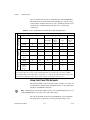
1
PXI Express NI PXIe-6672 User Manual Timing and Synchronization Module for PXI Express NI PXIe-6672 User Manual June 2008 372185F-01 Support Worldwide Technical Support and Product Information ni.com National Instruments Corporate Headquarters 11500 North Mopac Expressway Austin, Texas 78759-3504 USA Tel: 512 683 0100 Worldwide Offices Australia 1800 300 800, Austria 43 662 457990-0, Belgium 32 (0) 2 757 0020, Brazil 55 11 3262 3599, Canada 800 433 3488, China 86 21 5050 9800, Czech Republic 420 224 235 774, Denmark 45 45 76 26 00, Finland 358 (0) 9 725 72511, France 01 57 66 24 24, Germany 49 89 7413130, India 91 80 41190000, Israel 972 3 6393737, Italy 39 02 41309277, Japan 0120-527196, Korea 82 02 3451 3400, Lebanon 961 (0) 1 33 28 28, Malaysia 1800 887710, Mexico 01 800 010 0793, Netherlands 31 (0) 348 433 466, New Zealand 0800 553 322, Norway 47 (0) 66 90 76 60, Poland 48 22 3390150, Portugal 351 210 311 210, Russia 7 495 783 6851, Singapore 1800 226 5886, Slovenia 386 3 425 42 00, South Africa 27 0 11 805 8197, Spain 34 91 640 0085, Sweden 46 (0) 8 587 895 00, Switzerland 41 56 2005151, Taiwan 886 02 2377 2222, Thailand 662 278 6777, Turkey 90 212 279 3031, United Kingdom 44 (0) 1635 523545 For further support information, refer to the Technical Support and Professional Services appendix. To comment on National Instruments documentation, refer to the National Instruments Web site at ni.com/info and enter the info code feedback. © 2007–2008 National Instruments Corporation. All rights reserved. Important Information Warranty The NI PXIe-6672 is warranted against defects in materials and workmanship for a period of one year from the date of shipment, as evidenced by receipts or other documentation. National Instruments will, at its option, repair or replace equipment that proves to be defective during the warranty period. This warranty includes parts and labor. The media on which you receive National Instruments software are warranted not to fail to execute programming instructions, due to defects in materials and workmanship, for a period of 90 days from date of shipment, as evidenced by receipts or other documentation. National Instruments will, at its option, repair or replace software media that do not execute programming instructions if National Instruments receives notice of such defects during the warranty period. National Instruments does not warrant that the operation of the software shall be uninterrupted or error free. A Return Material Authorization (RMA) number must be obtained from the factory and clearly marked on the outside of the package before any equipment will be accepted for warranty work. National Instruments will pay the shipping costs of returning to the owner parts which are covered by warranty. National Instruments believes that the information in this document is accurate. The document has been carefully reviewed for technical accuracy. In the event that technical or typographical errors exist, National Instruments reserves the right to make changes to subsequent editions of this document without prior notice to holders of this edition. The reader should consult National Instruments if errors are suspected. In no event shall National Instruments be liable for any damages arising out of or related to this document or the information contained in it. EXCEPT AS SPECIFIED HEREIN, NATIONAL INSTRUMENTS MAKES NO WARRANTIES, EXPRESS OR IMPLIED, AND SPECIFICALLY DISCLAIMS ANY WARRANTY OF MERCHANTABILITY OR FITNESS FOR A PARTICULAR PURPOSE. CUSTOMER’S RIGHT TO RECOVER DAMAGES CAUSED BY FAULT OR NEGLIGENCE ON THE PART OF NATIONAL INSTRUMENTS SHALL BE LIMITED TO THE AMOUNT THERETOFORE PAID BY THE CUSTOMER. NATIONAL INSTRUMENTS WILL NOT BE LIABLE FOR DAMAGES RESULTING FROM LOSS OF DATA, PROFITS, USE OF PRODUCTS, OR INCIDENTAL OR CONSEQUENTIAL DAMAGES, EVEN IF ADVISED OF THE POSSIBILITY THEREOF. This limitation of the liability of National Instruments will apply regardless of the form of action, whether in contract or tort, including negligence. Any action against National Instruments must be brought within one year after the cause of action accrues. National Instruments shall not be liable for any delay in performance due to causes beyond its reasonable control. The warranty provided herein does not cover damages, defects, malfunctions, or service failures caused by owner’s failure to follow the National Instruments installation, operation, or maintenance instructions; owner’s modification of the product; owner’s abuse, misuse, or negligent acts; and power failure or surges, fire, flood, accident, actions of third parties, or other events outside reasonable control. Copyright Under the copyright laws, this publication may not be reproduced or transmitted in any form, electronic or mechanical, including photocopying, recording, storing in an information retrieval system, or translating, in whole or in part, without the prior written consent of National Instruments Corporation. National Instruments respects the intellectual property of others, and we ask our users to do the same. NI software is protected by copyright and other intellectual property laws. Where NI software may be used to reproduce software or other materials belonging to others, you may use NI software only to reproduce materials that you may reproduce in accordance with the terms of any applicable license or other legal restriction. Trademarks National Instruments, NI, ni.com, and LabVIEW are trademarks of National Instruments Corporation. Refer to the Terms of Use section on ni.com/legal for more information about National Instruments trademarks. Other product and company names mentioned herein are trademarks or trade names of their respective companies. Members of the National Instruments Alliance Partner Program are business entities independent from National Instruments and have no agency, partnership, or joint-venture relationship with National Instruments. Patents For patents covering National Instruments products, refer to the appropriate location: Help»Patents in your software, the patents.txt file on your media, or ni.com/patents. WARNING REGARDING USE OF NATIONAL INSTRUMENTS PRODUCTS (1) NATIONAL INSTRUMENTS PRODUCTS ARE NOT DESIGNED WITH COMPONENTS AND TESTING FOR A LEVEL OF RELIABILITY SUITABLE FOR USE IN OR IN CONNECTION WITH SURGICAL IMPLANTS OR AS CRITICAL COMPONENTS IN ANY LIFE SUPPORT SYSTEMS WHOSE FAILURE TO PERFORM CAN REASONABLY BE EXPECTED TO CAUSE SIGNIFICANT INJURY TO A HUMAN. (2) IN ANY APPLICATION, INCLUDING THE ABOVE, RELIABILITY OF OPERATION OF THE SOFTWARE PRODUCTS CAN BE IMPAIRED BY ADVERSE FACTORS, INCLUDING BUT NOT LIMITED TO FLUCTUATIONS IN ELECTRICAL POWER SUPPLY, COMPUTER HARDWARE MALFUNCTIONS, COMPUTER OPERATING SYSTEM SOFTWARE FITNESS, FITNESS OF COMPILERS AND DEVELOPMENT SOFTWARE USED TO DEVELOP AN APPLICATION, INSTALLATION ERRORS, SOFTWARE AND HARDWARE COMPATIBILITY PROBLEMS, MALFUNCTIONS OR FAILURES OF ELECTRONIC MONITORING OR CONTROL DEVICES, TRANSIENT FAILURES OF ELECTRONIC SYSTEMS (HARDWARE AND/OR SOFTWARE), UNANTICIPATED USES OR MISUSES, OR ERRORS ON THE PART OF THE USER OR APPLICATIONS DESIGNER (ADVERSE FACTORS SUCH AS THESE ARE HEREAFTER COLLECTIVELY TERMED “SYSTEM FAILURES”). ANY APPLICATION WHERE A SYSTEM FAILURE WOULD CREATE A RISK OF HARM TO PROPERTY OR PERSONS (INCLUDING THE RISK OF BODILY INJURY AND DEATH) SHOULD NOT BE RELIANT SOLELY UPON ONE FORM OF ELECTRONIC SYSTEM DUE TO THE RISK OF SYSTEM FAILURE. TO AVOID DAMAGE, INJURY, OR DEATH, THE USER OR APPLICATION DESIGNER MUST TAKE REASONABLY PRUDENT STEPS TO PROTECT AGAINST SYSTEM FAILURES, INCLUDING BUT NOT LIMITED TO BACK-UP OR SHUT DOWN MECHANISMS. BECAUSE EACH END-USER SYSTEM IS CUSTOMIZED AND DIFFERS FROM NATIONAL INSTRUMENTS' TESTING PLATFORMS AND BECAUSE A USER OR APPLICATION DESIGNER MAY USE NATIONAL INSTRUMENTS PRODUCTS IN COMBINATION WITH OTHER PRODUCTS IN A MANNER NOT EVALUATED OR CONTEMPLATED BY NATIONAL INSTRUMENTS, THE USER OR APPLICATION DESIGNER IS ULTIMATELY RESPONSIBLE FOR VERIFYING AND VALIDATING THE SUITABILITY OF NATIONAL INSTRUMENTS PRODUCTS WHENEVER NATIONAL INSTRUMENTS PRODUCTS ARE INCORPORATED IN A SYSTEM OR APPLICATION, INCLUDING, WITHOUT LIMITATION, THE APPROPRIATE DESIGN, PROCESS AND SAFETY LEVEL OF SUCH SYSTEM OR APPLICATION. Contents About This Manual Conventions ...................................................................................................................vii National Instruments Documentation ............................................................................viii Related Documentation..................................................................................................viii Chapter 1 Introduction What You Need to Get Started ......................................................................................1-1 Unpacking ......................................................................................................................1-2 Software Programming Choices ....................................................................................1-2 Safety Information .........................................................................................................1-3 Chapter 2 Installing and Configuring Installing the Software ...................................................................................................2-1 Installing the Hardware..................................................................................................2-1 Configuring the Module.................................................................................................2-2 Chapter 3 Hardware Overview NI PXIe-6672 Front Panel .............................................................................................3-3 Access LED .....................................................................................................3-4 Active LED......................................................................................................3-4 Connectors.......................................................................................................3-5 Hardware Features .........................................................................................................3-5 Clock Generation ...........................................................................................................3-7 Direct Digital Synthesis (DDS) .......................................................................3-7 PXI_CLK10 and TCXO ..................................................................................3-8 Routing Signals..............................................................................................................3-9 Determining Sources and Destinations ...........................................................3-11 Using Front Panel PFIs As Inputs.....................................................3-12 Using Front Panel PFIs As Outputs ..................................................3-13 Using the PXI Triggers .....................................................................3-14 Using the PXI Star Triggers..............................................................3-15 © National Instruments Corporation v NI PXIe-6672 User Manual Contents Choosing the Type of Routing ........................................................................ 3-15 Asynchronous Routing ..................................................................... 3-16 Synchronous Routing ....................................................................... 3-17 Generating a Single Pulse (Global Software Trigger) .................................... 3-18 Using the PXI_CLK10 PLL .......................................................................................... 3-19 Chapter 4 Calibration Factory Calibration........................................................................................................ 4-1 TCXO Frequency ............................................................................................ 4-1 PXI_CLK10 Phase.......................................................................................... 4-1 DDS Start Trigger Phase................................................................................. 4-1 DDS Initial Phase............................................................................................ 4-2 Additional Information.................................................................................................. 4-2 Appendix A Specifications Appendix B Technical Support and Professional Services Glossary Index NI PXIe-6672 User Manual vi ni.com About This Manual Thank you for purchasing the National Instruments NI PXIe-6672 Timing and Synchronization Module. The NI PXIe-6672 enables you to pass PXI timing and trigger signals between two or more PXI Express chassis. The NI PXIe-6672 can generate and route clock signals between devices in multiple chassis, providing a method to synchronize multiple devices in a multichassis PXI Express system. This manual describes the electrical and mechanical aspects of the NI PXIe-6672 and contains information concerning its operation and programming. Conventions The following conventions appear in this manual: <> Angle brackets that contain numbers separated by an ellipsis represent a range of values associated with a bit or signal name—for example, AO <3..0>. » The » symbol leads you through nested menu items and dialog box options to a final action. The sequence File»Page Setup»Options directs you to pull down the File menu, select the Page Setup item, and select Options from the last dialog box. This icon denotes a tip, which alerts you to advisory information. This icon denotes a note, which alerts you to important information. This icon denotes a caution, which advises you of precautions to take to avoid injury, data loss, or a system crash. When this symbol is marked on the product, refer to the Safety Information section of Chapter 1, Introduction, for precautions to take. bold Bold text denotes items that you must select or click in the software, such as menu items and dialog box options. Bold text also denotes parameter names and hardware labels. italic Italic text denotes variables, emphasis, a cross-reference, or an introduction to a key concept. Italic text also denotes text that is a placeholder for a word or value that you must supply. © National Instruments Corporation vii NI PXIe-6672 User Manual About This Manual monospace Text in this font denotes text or characters that you should enter from the keyboard, sections of code, programming examples, and syntax examples. This font is also used for the proper names of disk drives, paths, directories, programs, subprograms, subroutines, device names, functions, operations, variables, filenames, and extensions. NI PXIe-6672 This phrase refers to the NI PXIe-6672 module for the PXI Express bus. National Instruments Documentation The NI PXIe-6672 User Manual is one piece of the documentation set for your measurement system. You could have any of several other documents describing your hardware and software. Use the documentation you have as follows: • Measurement hardware documentation—This documentation contains detailed information about the measurement hardware that plugs into or is connected to the computer. Use this documentation for hardware installation and configuration instructions, specifications about the measurement hardware, and application hints. • Software documentation—Refer to the NI-Sync User Manual, available at ni.com/manuals. You can download NI documentation from ni.com/manuals. Related Documentation The following documents contain information that you might find helpful as you read this manual: NI PXIe-6672 User Manual • PICMG 2.0 R3.0, CompactPCI Core Specification, available from PICMG at www.picmg.org • PXI-5 PXI Express Hardware Specification, Revision 1.0, available from www.pxisa.org • NI-VISA User Manual, available from ni.com/manuals • NI-VISA Help, included with the NI-VISA software • NI-Sync User Manual, available from ni.com/manuals viii ni.com 1 Introduction The NI PXIe-6672 timing and triggering module enables you to pass PXI timing signals between two or more PXI Express chassis. The NI PXIe-6672 module generates and routes clock signals between devices in multiple chassis, providing a method for synchronizing multiple devices in a PXI Express system. What You Need to Get Started To set up and use the NI PXIe-6672, you need the following items: ❑ NI PXIe-6672 Timing and Triggering Module ❑ NI PXIe-6672 User Manual ❑ NI-Sync CD ❑ An Application Development Environment such as: – LabVIEW – LabWindows™/CVI™ – Microsoft Visual C++ (MSVC) ❑ PXI Express chassis ❑ PXI Express embedded controller or a desktop computer connected to the PXI Express chassis using MXI-Express hardware For information on using the driver software for synchronization, refer to the NI-Sync User Manual, which you can find on the NI-Sync CD or download from ni.com/manuals. © National Instruments Corporation 1-1 NI PXIe-6672 User Manual Chapter 1 Introduction Unpacking The NI PXIe-6672 is shipped in an antistatic package to prevent electrostatic damage to the module. Electrostatic discharge (ESD) can damage several components on the module. Caution Never touch the exposed pins of connectors. To avoid such damage in handling the module, take the following precautions: • Ground yourself using a grounding strap or by touching a grounded object. • Touch the antistatic package to a metal part of the computer chassis before removing the module from the package. Remove the module from the package and inspect the module for loose components or any sign of damage. Notify NI if the module appears damaged in any way. Do not install a damaged module into the computer. Store the NI PXIe-6672 in the antistatic envelope when not in use. Software Programming Choices When programming the NI PXIe-6672, you can use NI application development environment (ADE) software such as LabVIEW or LabWindows/CVI, or you can use other ADEs such as Visual C/C++. LabVIEW features interactive graphics, a state-of-the-art interface, and a powerful graphical programming language. The LabVIEW Data Acquisition VI Library, a series of virtual instruments for using LabVIEW with National Instruments DAQ hardware, is included with LabVIEW. LabWindows/CVI is a complete ANSI C ADE that features an interactive user interface, code generation tools, and the LabWindows/CVI Data Acquisition and Easy I/O libraries. NI PXIe-6672 User Manual 1-2 ni.com Chapter 1 Introduction Safety Information The following section contains important safety information that you must follow when installing and using the product. Do not operate the product in a manner not specified in this document. Misuse of the product can result in a hazard. You can compromise the safety protection built into the product if the product is damaged in any way. If the product is damaged, return it to National Instruments for repair. Do not substitute parts or modify the product except as described in this document. Use the product only with the chassis, modules, accessories, and cables specified in the installation instructions. You must have all covers and filler panels installed during operation of the product. Do not operate the product in an explosive atmosphere or where there may be flammable gases or fumes. If you must operate the product in such an environment, it must be in a suitably rated enclosure. If you need to clean the product, use a soft, nonmetallic brush. The product must be completely dry and free from contaminants before you return it to service. Operate the product only at or below Pollution Degree 2. Pollution is foreign matter in a solid, liquid, or gaseous state that can reduce dielectric strength or surface resistivity. The following is a description of pollution degrees: • Pollution Degree 1 means no pollution or only dry, nonconductive pollution occurs. The pollution has no influence. • Pollution Degree 2 means that only nonconductive pollution occurs in most cases. Occasionally, however, a temporary conductivity caused by condensation must be expected. • Pollution Degree 3 means that conductive pollution occurs, or dry, nonconductive pollution occurs that becomes conductive due to condensation. You must insulate signal connections for the maximum voltage for which the product is rated. Do not exceed the maximum ratings for the product. Do not install wiring while the product is live with electrical signals. Do not remove or add connector blocks when power is connected to the system. Avoid contact between your body and the connector block signal when hot swapping modules. Remove power from signal lines before connecting them to or disconnecting them from the product. © National Instruments Corporation 1-3 NI PXIe-6672 User Manual Chapter 1 Introduction Operate the product at or below the installation category1 marked on the hardware label. Measurement circuits are subjected to working voltages2 and transient stresses (overvoltage) from the circuit to which they are connected during measurement or test. Installation categories establish standard impulse withstand voltage levels that commonly occur in electrical distribution systems. The following is a description of installation categories: 1 2 3 • Installation Category I is for measurements performed on circuits not directly connected to the electrical distribution system referred to as MAINS3 voltage. This category is for measurements of voltages from specially protected secondary circuits. Such voltage measurements include signal levels, special equipment, limited-energy parts of equipment, circuits powered by regulated low-voltage sources, and electronics. • Installation Category II is for measurements performed on circuits directly connected to the electrical distribution system. This category refers to local-level electrical distribution, such as that provided by a standard wall outlet (for example, 115 V for U.S. or 230 V for Europe). Examples of Installation Category II are measurements performed on household appliances, portable tools, and similar products. • Installation Category III is for measurements performed in the building installation at the distribution level. This category refers to measurements on hard-wired equipment such as equipment in fixed installations, distribution boards, and circuit breakers. Other examples are wiring, including cables, bus-bars, junction boxes, switches, socket-outlets in the fixed installation, and stationary motors with permanent connections to fixed installations. • Installation Category IV is for measurements performed at the primary electrical supply installation (<1,000 V). Examples include electricity meters and measurements on primary overcurrent protection devices and on ripple control units. Installation categories, also referred to as measurement categories, are defined in electrical safety standard IEC 61010-1. Working voltage is the highest rms value of an AC or DC voltage that can occur across any particular insulation. MAINS is defined as a hazardous live electrical supply system that powers equipment. Suitably rated measuring circuits may be connected to the MAINS for measuring purposes. NI PXIe-6672 User Manual 1-4 ni.com Installing and Configuring 2 This chapter describes how to install the NI PXIe-6672 hardware and software and how to configure the device. Installing the Software Refer to the readme.htm file that accompanies the NI-Sync CD for software installation directions. Note Be sure to install the driver software before installing the NI PXIe-6672 hardware. Installing the Hardware The following are general installation instructions. Consult the chassis user manual or technical reference manual for specific instructions and warnings about installing new modules. 1. Power off and unplug the chassis. 2. Locate the System Timing Slot in your chassis. It is marked by either a square glyph shown in Figure 2-1, or a square glyph with a circle inside of it, as shown in Figure 2-2. Figure 2-1. System Timing Device Slot Indicator Glyph without Circle Figure 2-2. System Timing Device Slot Indicator Glyph on the NI PXIe-1062Q Chassis © National Instruments Corporation 2-1 NI PXIe-6672 User Manual Chapter 2 Installing and Configuring Note The slot number printed on the glyph may vary from chassis to chassis. The circle inside of the square indicates that the slot may also be used as a PXI Express peripheral slot. 3. Remove the filler panel for the PXI slot you located in step 2. 4. Ground yourself using a grounding strap or by holding a grounded object. Follow the ESD protection precautions described in the Unpacking section of Chapter 1, Introduction. 5. Remove any packing material from the front panel screws and backplane connectors. 6. Insert the NI PXIe-6672 into the PXI Express slot. Use the injector/ejector handle to fully insert the module into the chassis. 7. Screw the front panel of the device to the front panel mounting rail of the chassis. 8. Visually verify the installation. Make sure the module is not touching other modules or components and is fully inserted into the slot. 9. Plug in and power on the chassis. The NI PXIe-6672 is now installed. Configuring the Module The NI PXIe-6672 is completely software configurable. The system software automatically allocates all module resources. The two LEDs on the front panel provide information about module status. The front panel description sections of Chapter 3, Hardware Overview, describe the LEDs in greater detail. NI PXIe-6672 User Manual 2-2 ni.com 3 Hardware Overview This chapter presents an overview of the hardware functions of the NI PXIe-6672. Figure 3-1 provides a functional overview of the NI PXIe-6672 hardware. © National Instruments Corporation 3-1 NI PXIe-6672 User Manual Chapter 3 CLKIN Hardware Overview PXI_CLK10_IN AC Coupled Clock Detector PLL TCXO Calibration DAC PXI_CLK10 PXI TCXO Clock TCXO CLKOUT CLKIN DDS DDS Clock PFI 0 Driver/ Comparator CLOCK and TRIGGER Routing PFI 0 Threshold DAC PFI 1 PXI_STAR<0..16> PXI_TRIG<0..7> Driver/ Comparator PFI 1 Threshold DAC Driver/ Comparator PCI Interface PCI PFI 2 PFI 2 Threshold DAC PFI 3 Driver/ Comparator PFI 3 Threshold DAC PFI 4 Driver/ Comparator PFI 4 Threshold DAC PFI 5 Driver/ Comparator PFI 5 Threshold DAC Figure 3-1. Functional Overview of the NI PXIe-6672 NI PXIe-6672 User Manual 3-2 ni.com Chapter 3 Hardware Overview NI PXIe-6672 Front Panel Figure 3-2 shows the connectors and LEDs on the front panel of the NI PXIe-6672. NI PXIe-6672 Timing Module 1 2 ACCESS ACTIVE 3 CLK OUT 4 CLK IN PFI 0 PFI 1 PFI 2 5 PFI 3 PFI 4 PFI 5 1 2 3 Access LED Active LED CLKOUT Connector 4 5 CLKIN Connector PFI <0..5> Connectors Figure 3-2. NI PXIe-6672 Front Panel © National Instruments Corporation 3-3 NI PXIe-6672 User Manual Chapter 3 Hardware Overview Access LED The Access LED indicates the communication status of the NI PXIe-6672. Refer to Figure 3-2 for the location of the Access LED. Table 3-1 summarizes what the Access LED colors represent. Table 3-1. Access LED Color Indication Color Status Off Module is not yet functional. Green Driver has initialized the module. Amber Module is being accessed. The Access LED flashes amber for 50 ms when the module is accessed. Active LED The Active LED can indicate an error or phase-locked loop (PLL) activity. You can change the Active LED to amber, unless an error overrides the selection. Refer to Figure 3-2 for the location of the Active LED. Changing the Active LED color to amber is helpful when you want to identify devices in a multichassis situation or when you want an indication that your application has reached a predetermined section of the code. Tip Table 3-2 illustrates the meaning of each Active LED color. Table 3-2. Active LED Color Quick Reference Table Color PXI_CLK10 Stopped PLL Error User Setting PLL Active Red Yes Yes — — Amber No No Yes — Green No No No Yes Off No No No No Note A red Active LED can indicate that either PXI_CLK10 has stopped or that there is a PLL error. NI PXIe-6672 User Manual 3-4 ni.com Chapter 3 Hardware Overview Connectors This section describes the connectors on the front panel of the NI PXIe-6672. • CLKIN—Clock Input. This connector supplies the module with a clock that can be programmatically routed to the onboard PLL for use as a reference or routed directly to the PXI backplane (PXI_CLK10_IN) for distribution to the other modules in the chassis. • CLKOUT—Clock Output. This connector is used to source a clock that can be routed programmatically from the temperature-compensated crystal oscillator (TCXO), direct digital synthesis (DDS), or backplane clock (PXI_CLK10). • PFI <0..5>—Programmable Function Interface <0..5>. These connectors can be used for either input or output. Additionally, PFI 0 can be used as a clock input for internally synchronizing other signals. Refer to the Synchronous Routing section for more information about this functionality. You can program the behavior of these PFI connections individually. Refer to Figure 3-2 for a diagram showing the locations of these connections on the NI PXIe-6672 front panel. Connections that exceed any of the maximum ratings of input or output signals on the NI PXIe-6672 can damage the module and the computer. NI is not liable for any damage resulting from such signal connections. Caution Hardware Features The NI PXIe-6672 perform two broad functions: • Generating clock and trigger signals • Routing internally or externally generated signals from one location to another © National Instruments Corporation 3-5 NI PXIe-6672 User Manual Chapter 3 Hardware Overview Table 3-3 outlines the function and direction of the signals discussed in detail in the remainder of this chapter. Table 3-3. Signal Descriptions Signal Name Direction Description Out This is a signal that can replace the native 10 MHz oscillator on the PXI backplane. PXI_CLK10_IN may originate from the onboard TCXO or from an external source. PXI_CLK10 In This signal is the PXI 10 MHz backplane clock. By default, this signal is the output of the native 10 MHz oscillator in the chassis. An NI PXIe-6672 in the System Timing Slot can replace this signal with PXI_CLK10_IN. TCXO Clock Out This is the output of the 10 MHz TCXO. The TCXO is an extremely stable and accurate frequency source. In CLKIN is a signal connected to the SMB input pin of the same name. CLKIN can serve as PXI_CLK10_IN, a phase lock reference for the TCXO, or as a source for routing to PXI_STAR. CLKOUT Out CLKOUT is the signal on the SMB output pin of the same name. Either the TCXO clock, DDS clock, or PXI_CLK10 may be routed to this location. DDS Clock Out This is the output of the DDS. The DDS frequency can be programmed with fine granularity from 1 Hz to 105 MHz. The DDS chip automatically phase-locks to PXI_CLK10. PXI_STAR <0..16> In/Out The PXI star trigger bus connects the System Timing Slot to all other slots in a star configuration. The electrical paths of each star line are closely matched to minimize intermodule skew. An NI PXIe-6672 in System Timing Slot can route signals to all other slots using the star trigger bus. PFI <0..5> In/Out The Programmable Function Interface pins on the NI PXIe-6672 route timing and triggering signals between multiple PXI chassis. A wide variety of input and output signals can be routed to or from the PFI lines. PXI_TRIG <0..7> In/Out The PXI trigger bus consists of eight digital lines shared among all slots in the PXI chassis. The NI PXIe-6672 can route a wide variety of signals to and from these lines. PXI_CLK10_IN CLKIN NI PXIe-6672 User Manual 3-6 ni.com Chapter 3 Hardware Overview The remainder of this chapter describes how these signals are used, acquired, and generated by the NI PXIe-6672 hardware, and explains how you can route the signals between various locations to synchronize multiple measurement devices and PXI chassis. Clock Generation The NI PXIe-6672 can generate two types of clock signals. The first clock is generated using the onboard DDS chip, and the second is generated with a precise 10 MHz oscillator. The following sections describe the two types of clock generation and explain the considerations for choosing either type. Direct Digital Synthesis (DDS) DDS is a method of generating a clock with programmable frequency. DDS consists of a frequency tuning word, an accumulator, a sine-lookup table, a D/A converter (DAC), and a comparator. The frequency tuning word is a number that specifies the desired frequency. Each master clock cycle, the frequency tuning word is added to the accumulator, which rolls over when it gets to its maximum value. The accumulator value is used to get a point in the sine-lookup table, which is converted to an analog voltage by the DAC. For example, if the sine table is 128 points long, and the frequency tuning word is one, the accumulator takes 128 clock cycles to output one sine wave. If you change the frequency tuning word to 3, the accumulator steps through the sine table three times as fast, and outputs a sine wave in 128/3, or 42.6, clock cycles. The output of the DAC is run through an analog filter to smooth the sine wave. The filtered output is then run through a comparator, which changes the output to a square wave with the specified frequency. You can specify the programmable DDS frequency on the NI PXIe-6672 with a precision of approximately .07 Hz within the range 1 Hz to 105 MHz. The accuracy of the frequency depends on the PXI_CLK10 reference clock, so a precise 10 MHz source improves the accuracy of the DDS output. You can replace the 10 MHz clock with the TCXO for more accurate DDS timing. When the DDS is programmed an update signal must be sent to it before it will begin operating as programmed. The source for this update signal is either immediate (DDS starts outputting the programmed frequency as soon as software programs it) or one of the eight PXI triggers. When one © National Instruments Corporation 3-7 NI PXIe-6672 User Manual Chapter 3 Hardware Overview of the PXI trigger lines is used as the source for the update, frequency generation will not start until a rising edge occurs on the PXI trigger selected. NI-Sync software defaults to an immediate update. If a PXI trigger is used instead, the user must specify the update signal source before setting any of the other DDS properties. Note When more then one NI PXIe-6672 is used in a multiple chassis setup, the DDS frequency of both boards can be synchronized. The DDS system clock is phase locked to PXI_CLK10, when two or more chassis share a common 10 MHz clock, the DDS outputs will also be phase locked (refer to the Using the PXI_CLK10 PLL section for information on how to ensure that two or more chassis have close PXI_CLK10 phase alignment). To fully synchronize the DDS outputs a common update signal source must be used and routed to the selected PXI trigger. A synchronous route to PXI_CLK10 provides the best results. Refer to the Routing Signals section for details on routing trigger signals. The NI PXIe-6672 DDS can adjust the phase of the generated clock by up to ±5 ns. This may be used to tighten the synchronization between two or more DDS devices in a multi-chassis setup, or to compensate for delays caused by different cable lengths. PXI_CLK10 and TCXO The NI PXIe-6672 features a precision 10 MHz TCXO. The frequency accuracy of this clock is several orders of magnitude greater than the frequency accuracy of the native 10 MHz PXI backplane clock (PXI_CLK10). The TCXO contains circuitry to measure the temperature of the oscillator. It uses the temperature to adjust its frequency output according to the crystal’s known frequency variation across its operating temperature range. An NI PXIe-6672 module in the System Timing Slot of a PXI Express chassis can replace the native PXI 10 MHz backplane frequency reference clock (PXI_CLK10) with the more stable and accurate output of the TCXO. All other PXI modules in the chassis that reference the 10 MHz backplane clock benefit from this more accurate frequency reference. Furthermore, the DDS chip on the NI PXIe-6672 references its output to the backplane clock and also takes advantage of the superior TCXO accuracy. The TCXO does not automatically replace the native 10 MHz NI PXIe-6672 User Manual 3-8 ni.com Chapter 3 Hardware Overview clock; this feature must be explicitly enabled in software. The TCXO output also can be routed out to the CLKOUT connector. In addition to replacing the native backplane clock directly, the TCXO can phase lock to an external frequency source. This operation is discussed in detail in the Using the PXI_CLK10 PLL section. Routing Signals The NI PXIe-6672 has versatile trigger routing capabilities. It can route signals to and from the front panel, the PXI triggers, and the PXI star triggers. The CLKIN SMB input on the NI PXIe-6672 may be used for PXI_CLK10 replacement by either routing a 10 MHz signal directly from the CLKIN input to PXI_CLK10_IN, or by using the CLKIN input as a phase lock reference for the TCXO. When phase locking the TCXO to CLKIN, CLKIN may be any multiple of 1 MHz to 105 MHz. In addition, CLKIN is a valid source for PXI_Star. The CLKOUT SMB on the NI PXIe-6672 may also be used to route the TCXO, PXI_CLK10, or DDS Clock. © National Instruments Corporation 3-9 NI PXIe-6672 User Manual Chapter 3 Hardware Overview Figures 3-3 and 3-4 summarize the routing features of the NI PXIe-6672. The remainder of this chapter details the capabilities and constraints of the routing architecture. PFI 0 Selection Circuitry PFI 1 Selection Circuitry PFI 5 Selection Circuitry * PXI_STAR<0..16>, 28 PXI_TRIG<0..7>, PFI<0..5>, and Software Trigger are routed to SOURCE of each Selection Circuitry block. SOURCE* Selection Circuitry PXI_STAR 0 CLKIN Selection Circuitry PXI_STAR 1 Selection Circuitry PXI_STAR 16 Selection Circuitry PXI_TRIG 0 Selection Circuitry PXI_TRIG 1 Selection Circuitry PXI_TRIG 7 3 SYNCHRONIZATION CLOCKS for PFI<0..5> PFI 0 DDS PXI_CLK10 ÷2N ÷2M PFI 0 DDS PXI_CLK10 ÷2N SYNCHRONIZATION CLOCKS for PXI_STAR<0..16> and PXI_TRIG<0..7> 3 ÷2M Figure 3-3. High-Level Schematic of NI PXIe-6672 Signal Routing Architecture NI PXIe-6672 User Manual 3-10 ni.com Chapter 3 Hardware Overview Figure 3-4 provides a more detailed view of the Selection Circuitry referenced in Figure 3-3. CLKIN* SOURCE PFI<0..5> PXI_TRIG<0..7> PXI_STAR<0..16> Software Trigger DESTINATION SYNCHRONIZATION CLOCKS GND CLK CLK/N CLK/M * CLKIN only valid for PXI_STAR Figure 3-4. Signal Selection Circuitry Diagram Determining Sources and Destinations All signal routing operations can be characterized by a source (input) and a destination. In addition, synchronous routing operations must also define a third signal known as the synchronization clock. Refer to the Choosing the Type of Routing section for more information on synchronous versus asynchronous routing. © National Instruments Corporation 3-11 NI PXIe-6672 User Manual Chapter 3 Hardware Overview Table 3-4 summarizes the sources and destinations of the NI PXIe-6672. The destinations are listed in the horizontal heading row, and the sources are listed in the column at the far left. A ✓ in a cell indicates that the source and destination combination defined by that cell is a valid routing combination. Table 3-4. Sources and Destinations for NI PXIe-6672 Signal Routing Operations Destinations Front Panel Front Panel PFI <0..5> PXI_ CLK10_IN PXI_Star Trigger <0..16> PXI TRIG <0..7> TCXO Reference PLL ✓* ✓* ✓ ✓ ✓* ✓ ✓ ✓ ✓ ✓† ✓† ✓† PXI_STAR <0..16> ✓ ✓ ✓ PXI TRIG <0..7> ✓ ✓ ✓ ✓* ✓* CLKIN Backplane PXI_ CLK10 Onboard Onboard CLKOUT PFI <0..5> Sources Backplane ✓ TCXO ✓ ✓* DDS ✓ ✓† ✓† ✓† ✓ ✓ ✓ Global Software Trigger ✓ * Can be accomplished in two stages by routing source to PXI_CLK10_IN, replacing PXI_CLK10 with PXI_CLK10_IN (occurs automatically in most chassis), and then routing PXI_CLK10 to the destination. The source must be 10 MHz. † Routing PXI_CLK10 or DDS to PFI, PXI_Star, or PXI_Trigger is accomplished by setting PXI_CLK10 or DDS to be the synchronization clock (NI-Sync Property Node) and then routing the synchronization clock as the source. Using Front Panel PFIs As Inputs The front-panel PFIs can receive external signals from 0 to +5 V. They can be terminated programmatically with 50 Ω resistances to match the cable impedance and minimize reflections. Note Terminating the signals with a 50 Ω resistance is recommended when the source is another NI PXIe-6672 or any other source with a 50 Ω output. The voltage thresholds for the front-panel PFI inputs are programmable. The input signal is generated by comparing the input voltage on the NI PXIe-6672 User Manual 3-12 ni.com Chapter 3 Hardware Overview PFI connectors to the voltage output of software-programmable DACs. The thresholds for the PFI lines are individually programmable, which is useful if you are importing signals from multiple sources with different voltage swings. The front panel PFI inputs can be routed to any PXI_Star triggers, PXI triggers, or other front panel PFI outputs. Using Front Panel PFIs As Outputs The front panel PFI outputs are +3.3 V drivers with 50 Ω output impedance. The outputs can drive 50 Ω loads, such as a 50 Ω coaxial cable with a 50 Ω receiver. This cable configuration is the recommended setup to minimize reflections. With this configuration, the receiver sees a single +1.6 V step—a +3.3 V step split across the 50 Ω resistors at the source and the destination. You also can drive a 50 Ω cable with a high-impedance load. The destination sees a single step to +3.3 V, but the source sees a reflection. This cable configuration is acceptable for low-frequency signals or short cables. You can select the signal source from the front panel triggers (PFI <0..5>), the PXI star triggers, the PXI triggers, or the synchronization clock (PXI_CLK10, the DDS clock, or PFI 0). The synchronization clock concept is explained in more detail in the Choosing the Type of Routing section. You can independently select the output signal source for each PFI line from one of the following sources: • Another PFI <0..5> • PXI triggers <0..7> (PXI_TRIG <0..7>) • PXI_STAR <0..16> • Global software trigger • PFI synchronization clock The PFI synchronization clock may be any of the following signals: • DDS clock • PXI_CLK10 • PFI 0 Input • Any of the previously listed signals divided by the first frequency divider (2n, up to 512) • Any of the previously listed signals divided by the second frequency divider (2m, up to 512) © National Instruments Corporation 3-13 NI PXIe-6672 User Manual Chapter 3 Hardware Overview Refer to the Choosing the Type of Routing section for more information on the synchronization clock. The PFI synchronization clock is the same for all routing operations in which PFI <0..5> is defined as the output, although the divide-down ratio for this clock (full rate, first divider, second divider) may be chosen on a per route basis. Note Using the PXI Triggers The PXI triggers go to all the slots in the chassis. All modules receive the same PXI triggers, so PXI trigger 0 is the same for Slot 2 as it is for Slot 3, and so on. This feature makes the PXI triggers convenient in situations where you want, for instance, to start an acquisition on several devices at the same time because all modules will receive the same trigger. The frequency on the PXI triggers should not exceed 20 MHz to preserve signal integrity. The signals do not reach each slot at precisely the same time. A difference of several nanoseconds between slots can occur in an eight-slot chassis. However, this delay is not a problem for many applications. You can route signals to the PXI triggers from PFI <0..5>, from the PXI star triggers, or from other PXI triggers. You also can route PXI_CLK10 or the DDS clock to a PXI trigger line (PXI_TRIG <0..7>) using the synchronization clock. You can independently select the output signal source for each PXI trigger line from one of the following sources: • PFI <0..5> • Another PXI trigger <0..7> (PXI_TRIG <0..7>) • PXI_STAR <0..16> • Global software trigger • PXI_Trig/PXI_Star synchronization clock The PXI_Trig/PXI_Star synchronization clock may be any of the following signals: NI PXIe-6672 User Manual • DDS clock • PXI_CLK10 • PFI 0 Input • Any of the previously listed signals divided by the first frequency divider (2n, up to 512) • Any of the previously listed signals divided by the second frequency divider (2m, up to 512) 3-14 ni.com Chapter 3 Hardware Overview Refer to the Choosing the Type of Routing section for more information about the synchronization clock. The PXI_Trig/PXI_Star synchronization clock is the same for all routing operations in which PXI_TRIG <0..7> or PXI_STAR <0..16> is defined as the output, although the divide-down ratio for this clock (full rate, first divider, second divider) may be chosen on a per route basis. Note Using the PXI Star Triggers There are up to 17 PXI star triggers per chassis. Each trigger line is a dedicated connection between the System Timing Slot and one other slot. The PXI Specification, Revision 2.1, requires that the propagation delay along each star trigger line be matched to within 1 ns. A typical upper limit for the skew in most NI PXI chassis is 500 ps. The low skew of the PXI star trigger bus is useful for applications that require triggers to arrive at several modules nearly simultaneously. The star trigger lines are bidirectional, so signals can be sent to System Timing Slot from a module in another slot or from System Timing Slot to the other module. You can independently select the output signal source for each PXI star trigger line from one of the following sources: • PFI <0..5> • PXI triggers <0..7> (PXI_TRIG <0..7>) • Another PXI star trigger line (PXI_STAR <0..16>) • Global software trigger • PXI_Trig/PXI_Star synchronization clock • CLKIN Refer to the Using the PXI Triggers section for more information on the PXI_Trig/PXI_Star synchronization clock. Choosing the Type of Routing The NI PXIe-6672 routes signals in one of two ways: asynchronously or synchronously. The following sections describe the two routing types and the considerations for choosing each type. © National Instruments Corporation 3-15 NI PXIe-6672 User Manual Chapter 3 Hardware Overview Asynchronous Routing Asynchronous routing is the most straightforward method of routing signals. Any asynchronous route can be defined in terms of two signal locations: a source and a destination. A digital pulse or train comes in on the source and is propagated to the destination. When the source signal goes from low to high, this rising edge is transferred to the destination after a propagation delay through the module. Figure 3-5 illustrates an asynchronous routing operation. Propagation Delay tpd Trigger Input Trigger Output Figure 3-5. Asynchronous Routing Operation Some delay is always associated with an asynchronous route, and this delay varies among NI PXIe-6672 modules, depending on variations in temperature and chassis voltage. Typical delay times in the NI PXIe-6672 for asynchronous routes between various sources and destinations are given in Appendix A, Specifications. Asynchronous routing works well if the total system delays are not too long for the application. Propagation delay could be caused by the following reasons: • Output delay on the source • Propagation delay of the signal across the backplane(s) and cable(s) • Propagation delay of the signal through the NI PXIe-6672 • Time for the receiver to recognize the signal Both the source and the destination of an asynchronous routing operation on the NI PXIe-6672 can be any of the following lines: NI PXIe-6672 User Manual • Any front panel PFI pin (PFI <0..5) • Any PXI star trigger line (PXI_STAR <0..16>) • Any PXI trigger line (PXI_TRIG <0..7>) 3-16 ni.com Chapter 3 Hardware Overview Synchronous Routing A synchronous routing operation is defined in terms of three signal locations: a source, a destination, and a synchronization clock. A digital signal comes in on the source and is propagated to the destination after the edge has been realigned with the synchronization clock. Unlike asynchronous routing, the output of a synchronous routing operation does not directly follow the input after a propagation delay. Instead, the output waits for the next rising edge of the clock before it follows the input. Thus, the output is said to be “synchronous” with this clock. Figure 3-6 shows a timing diagram that illustrates synchronous routing. Setup Time tsetup Hold Time thold Trigger Input Synchronization Clock Clock to Output Time, tCtoQ Trigger Output Figure 3-6. Synchronous Routing Operation Synchronous routing can send triggers to several places in the same clock cycle or send the trigger to those same places after a deterministic skew of a known number of clock cycles. If a signal arrives at two chassis within the same clock cycle, each NI PXIe-6672 realigns the signal with the synchronization clock and distributes it to the modules in each chassis at the same time. Synchronous routing can thus remove uncertainty about when triggers are received. If the delays through the system are such that an asynchronous trigger might arrive near the edge of the receiver clock, the receiver might see the signal in the first clock cycle, or it might see it in © National Instruments Corporation 3-17 NI PXIe-6672 User Manual Chapter 3 Hardware Overview the second clock cycle. However, by synchronizing the signal, you can eliminate the ambiguity, and the signal will always be seen in the second clock cycle. One useful feature of synchronous routing is that the signal can be propagated on either the rising or falling edge of the synchronization clock. In addition, the polarity of the destination signal can be inverted, which is useful when handling active-low digital signals. Possible sources for synchronous routing include the following sources: • Any front panel PFI pin • Any PXI star trigger line (PXI_STAR <0..16>) • Any PXI trigger line (PXI_TRIG <0..7>) • Global software trigger • The synchronization clock itself The possible destinations for a synchronous route are identical to those for an asynchronous route. The destinations include any front panel PFI pin, any PXI star trigger line, or any PXI trigger line. Note The synchronization clock for a synchronous route can be any of the following signals: • 10 MHz PXI backplane clock signal • DDS clock on the NI PXIe-6672 • Front panel PFI 0 Input • One of two “divided copies” of any of the previously listed three signals. The NI PXIe-6672 includes two clock-divider circuits that can divide the synchronization clock signals by any power of 2 up to 512. Refer to Figures 3-3 and 3-4 for an illustration of how the NI PXIe-6672 performs synchronous routing operations. Generating a Single Pulse (Global Software Trigger) The global software trigger is a single pulse with programmable delay that is fired on a software command. This signal is always routed synchronously with a clock. Therefore, asynchronous routing is not supported when the signal source is the global software trigger. The software trigger can be delayed by up to 15 clock cycles on a per route basis. This feature is useful if a single pulse must be sent to several NI PXIe-6672 User Manual 3-18 ni.com Chapter 3 Hardware Overview destinations with significantly different propagation delays. By delaying the pulse on the routes with shorter paths, you can compensate for the propagation delay. An example of such a situation would be when a trigger pulse must arrive nearly simultaneously at the local backplane and the backplane of another chassis separated by 50 m of coaxial cable. Using the PXI_CLK10 PLL A module in System Timing Slot of a PXI Express chassis can replace the PXI_CLK10 reference clock. The NI PXIe-6672 offers three options for this replacement. This section describes each option. • The first option is to replace PXI_CLK10 directly with the TCXO output on the NI PXIe-6672. This oscillator is a more stable and accurate reference than the native backplane clock. • The second option is to route a 10 MHz clock directly from CLKIN on the front panel to PXI_CLK10_IN, which is the pin on the backplane that will replace PXI_CLK10. There is a delay through the module, as well as a distribution delay on the backplane. These delays tend to be similar for chassis of the same model, so routing the same clock to a pair of chassis usually matches PXI_CLK10 to within a few nanoseconds. • The third option is to employ the NI PXIe-6672 PLL circuitry for the TCXO. As in option 1, the output of the TCXO replaces the native 10 MHz signal. However, this scheme also requires an input signal on CLKIN. This signal must be a stable clock, and its frequency must be a multiple of 1 MHz (5 MHz or 13 MHz, for example) between 1 MHz and 105 MHz. The PLL feedback circuit generates a voltage proportional to the phase difference between the reference input on PXI_CLK10 and the output of the TCXO. This PLL voltage output then tunes the output frequency of the TCXO. As long as the incoming signal is a stable 1 MHz frequency multiple, the PLL circuit quickly locks the TCXO to the reference, eliminating all phase drift between the two signals. Using the PLL provides several advantages over the other two options for replacing the PXI backplane clock: • CLKIN is not required to be 10 MHz. If you have a stable reference that is a multiple of 1 MHz, such as 13 or 5 MHz, you can frequency-lock the chassis to it. • If CLKIN stops or becomes disconnected, PXI_CLK10 is still present in the chassis. © National Instruments Corporation 3-19 NI PXIe-6672 User Manual Chapter 3 Hardware Overview • NI PXIe-6672 User Manual If CLKIN is 10 MHz, the NI PXIe-6672 can compensate for distribution delays in the backplane. The feedback in the PLL comes from PXI_CLK10. This PLL makes it possible for the NI PXIe-6672 to align clock edges at CLKIN with the edges of PXI_CLK10 that the modules receive. If you split an external (accurate) 10 MHz reference and route it to two chassis, they can both lock to it. The result is a tighter synchronization of PXI_CLK10 on the chassis. 3-20 ni.com 4 Calibration This chapter discusses the calibration of the NI PXIe-6672. Calibration consists of verifying the measurement accuracy of a device and correcting for any measurement error. The NI PXIe-6672 is factory calibrated before shipment at approximately 25 °C to the levels indicated in Appendix A, Specifications. The associated calibration constants—the corrections that were needed to meet specifications—are stored in the onboard nonvolatile memory (EEPROM). The driver software uses these stored values. Factory Calibration The factory calibration of the NI PXIe-6672 involves calculating and storing four calibration constants. These values control the accuracy of four features of the device, which are discussed in the following sections. TCXO Frequency The TCXO frequency can be varied over a small range. The output frequency of the TCXO is adjusted using this constant to meet the specification listed in Appendix A, Specifications. This calibration applies only to the NI PXIe-6672. PXI_CLK10 Phase When using the PLL to lock PXI_CLK10 to an external reference clock, the phase between the clocks can be adjusted. The time between rising edges of PXI_CLK10 and the input clock is minimized using this constant. DDS Start Trigger Phase To start the DDS reliably, the DDS start trigger must arrive within a certain window of time. The phase of the DDS start trigger is controlled by this constant to meet the setup and hold-time requirements of the DDS. © National Instruments Corporation 4-1 NI PXIe-6672 User Manual Chapter 4 Calibration DDS Initial Phase The phase of the DDS output is adjusted using this constant so that the DDS outputs from multiple NI PXIe-6672 modules are aligned. Additional Information Refer to ni.com/calibration for additional information on NI calibration services. NI PXIe-6672 User Manual 4-2 ni.com A Specifications CLKIN Characteristics CLKIN fundamental frequency range1 .................................... 1 MHz to 105 MHz, sine or square wave Input impedance..................................... 50 Ω, nominal Input coupling ........................................ AC Voltage range DC ................................................... ±20 V AC ................................................... 400 mVp-p to 5 Vp-p Absolute maximum input voltage2......... ±26 V, max CLKIN to PXI_CLK10_IN delay without PLL ........................................... 14 ns to 14.7 ns, typical CLKIN to PXI_CLK10 delay with PLL ................................................ ±1 ns, max CLKIN frequency accuracy requirement For PLL and TCXO ........................ ±5.0 ppm For replacing PXI_CLK10 (no PLL).......................................... ±100 ppm3 1 2 3 CLKIN fundamental frequency can be any multiple of 1 MHz within the range specified when the PLL is engaged and PXI_CLK10 is locking to it. The frequency must be 10 MHz when replacing PXI_CLK10 without the PLL. Stresses beyond those listed can cause permanent damage to the device. Exposure to absolute maximum rated conditions for extended periods of time can affect device reliability. Functional operation of the device outside the conditions indicated in the operational parts of the specification is not implied. This is a requirement of the PXI specification. © National Instruments Corporation A-1 NI PXIe-6672 User Manual Appendix A Specifications Jitter added to CLKIN Without PLL....................................0.5 psrms, 10 Hz to 100 kHz, typical With PLL .........................................0.6 psrms, 10 Hz to 100 kHz, typical Duty cycle distortion of CLKIN to PXI_CLK10_IN without PLL ................±1%, max Required input duty cycle when using PLL......................................45 to 55% CLKOUT Characteristics Output frequency From PXI_CLK10 ...........................10 MHz From TCXO.....................................10 MHz From DDS .......................................1 MHz1 to 105 MHz Duty cycle...............................................43 to 55%2 Output impedance...................................50 Ω, nominal Output coupling ......................................AC Amplitude, software configurable to two voltage levels (low and high drive) 1 2 Open Load Square Wave Low Drive 2.0 Vp-p, typical High Drive 5.0 Vp-p, typical 50 Ω Load Square Wave Low Drive 1.0 Vp-p, typical High Drive 2.5 Vp-p, typical The lower limit is load dependent because of the AC coupling. This limit is less than 1 MHz for high-impedance loads. The duty cycle specification covers both DDS range and TCXO. NI PXIe-6672 User Manual A-2 ni.com Appendix A Specifications Square wave rise/fall time (10 to 90%) Low drive ........................................ 0.5 ns min, 2.5 ns max High drive ....................................... 0.5 ns min, 2.5 ns max PFI <0..5> Input Characteristics Frequency range..................................... DC to 105 MHz Input impedance..................................... 50 Ω, nominal, or 1 kΩ ±10%, || 35 pF, software-selectable Input coupling ........................................ DC Voltage level .......................................... 0 to 5 V Absolute maximum input voltage1......... ±5.25 V, max Input threshold Voltage level ................................... 0 to 4.3 V, software-selectable Voltage resolution........................... 16.8 mV (8 bits) Error ................................................ ±40 mV Hysteresis ............................................... 50 mV Asynchronous delay, t pd PFI <0..5> to PXI_TRIG <0..7> output ................ 19 to 26 ns, typical PFI <0..5> to PXI_STAR <0..12> output ............. 10 to 19 ns, typical Synchronized trigger input setup time, tsetup2 ........................... 16.5 ns, typical Synchronized trigger input hold time, thold2 .............................. –9.9 ns, typical 1 2 Stresses beyond those listed can cause permanent damage to the device. Exposure to absolute maximum rated conditions for extended periods of time can affect device reliability. Functional operation of the device outside the conditions indicated in the operational parts of the specifications is not implied. Relative to PXI_CLK10 at the backplane connector. When PLL is used to route CLKIN to PXI_CLK10_IN, CLKIN and PXI_CLK10 are phase locked with ±1 ns max phase difference. Refer to the Synchronous Routing section of Chapter 3, Hardware Overview, for more details. © National Instruments Corporation A-3 NI PXIe-6672 User Manual Appendix A Specifications Output Characteristics Frequency range .....................................DC to 105 MHz Output impedance...................................50 Ω, nominal Output coupling ......................................DC Voltage level...........................................0 to 1.6 V into 50 Ω; 0 to 3.3 V into open circuit, typical Absolute maximum applied voltage1 ......±5.25 V, max PXI_CLK10 synchronized trigger clock to out time, t CtoQ2 ....................................10.7 ns, typical Output-to-output skew, synchronous......500 ps, typical PXI_STAR Trigger Characteristics PXI_STAR <0..16> to PXI_STAR <0..16> output skew at NI PXIe-6672 backplane connector....300 ps3, typical Asynchronous delays, t pd PXI_STAR <0..16> to PFI <0..5> output.............................13 to 17 ns, typical PXI_STAR <0..16> to PXI_TRIG <0..7> output.................18 to 24 ns, typical 1 2 3 Stresses beyond those listed can cause permanent damage to the device. Exposure to absolute maximum rated conditions for extended periods of time can affect device reliability. Functional operation of the device outside the conditions indicated in the operational parts of the specifications is not implied. Relative to PXI_CLK10 at backplane connector. This specification applies to all synchronous routes to the PXI_Star lines, as well as asynchronous routes from the PFI inputs to the PXI_Star lines. NI PXIe-6672 User Manual A-4 ni.com Appendix A Specifications PXI Trigger Characteristics PXI_TRIG <0..7> to PXI_TRIG <0..7> output skew at NI PXIe-6672 backplane connector ... 5 ns, typical Asynchronous delay, t pd PXI_TRIG <0..7> to PFI <0..5> output ............................ 15 to 22 ns, typical TCXO Characteristics Frequency............................................... 10 MHz Initial accuracy ....................................... ±2.5 ppm Long-term stability (1 year)1 .................. ±1 ppm Temperature stability (0 to 55 °C)2 ........ ±2 ppm DDS Characteristics Frequency range..................................... 1 Hz to 105 MHz Frequency resolution.............................. < 0.075 Hz Frequency accuracy................................ Equivalent to PXI_CLK10 accuracy3 Physical Chassis requirement ............................... One 3U PXI Express System Timing Slot Front panel connectors ........................... SMB male, 50 Ω Front panel indicators............................. Two tricolor LEDs (green, red, and amber) 1 2 3 Includes stability of TCXO and supporting circuitry. Includes temperature stability of TCXO and supporting circuitry. The DDS frequency inherits the relative frequency of PXI_CLK10. For example, if you route the TCXO to PXI_CLK10, the DDS output inherits the same relative frequency accuracy as the TCXO output. © National Instruments Corporation A-5 NI PXIe-6672 User Manual Appendix A Specifications Recommended maximum cable length1 PFI/CLKOUT, DC to 10 MHz ........200 m CLKOUT High Gain, 105 MHz......80 m2 PFI/CLKOUT Low Gain, 105 MHz..........................................30 m3 Weight ....................................................0.459 lb (208 g) Power Requirements +3.3 V .....................................................800 mA, max +12 V ......................................................700 mA, max Environment Maximum altitude...................................2,000 m (800 mbar) (at 25 °C ambient temperature) Pollution Degree .....................................2 Indoor use only. When required, clean the NI PXIe-6672 with a soft nonmetallic brush. Make sure that the device is completely dry and free from contaminants before returning it to service. Caution Operating Environment Ambient temperature range ....................0 to 55 °C (Tested in accordance with IEC-60068-2-1 and IEC-60068-2-2. Meets MIL-PRF-28800F Class 3 low temperature limit and MIL-PRF-28800F Class 2 high temperature limit.) Relative humidity range..........................10% to 90%, noncondensing (Tested in accordance with IEC-60068-2-56.) 1 2 3 Cable length measurements were made with an RG 58 cable. Maximum cable length performance will vary depending on the cable type used. Maximum cable length with a direct cable connection. Loss from a signal splitter would reduce maximum cable length. Maximum cable length with a direct cable connection. Loss from a signal splitter would reduce maximum cable length. NI PXIe-6672 User Manual A-6 ni.com Appendix A Specifications Storage Environment Ambient temperature range.................... –40 to 71 °C (Tested in accordance with IEC-60068-2-1 and IEC-60068-2-2. Meets MIL-PRF-28800F Class 3 low temperature limit.) Relative humidity range ......................... 5% to 95% noncondensing (Tested in accordance with IEC-60068-2-56.) Shock and Vibration Operational shock .................................. 30 g peak, half-sine, 11 ms pulse (Tested in accordance with IEC-60068-2-27. Meets MIL-PRF-28800F Class 2 limits.) Random vibration Operating ........................................ 5 to 500 Hz, 0.3 grms Nonoperating .................................. 5 to 500 Hz, 2.4 grms (Tested in accordance with IEC-60068-2-64. Nonoperating test profile exceeds the requirements of MIL-PRF-28800F, Class 3.) Note Specifications are subject to change without notice. Safety This product is designed to meet the requirements of the following standards of safety for electrical equipment for measurement, control, and laboratory use: • • IEC 61010-1, EN 61010-1 • • UL 61010-1, CSA 61010-1 Note For UL and other safety certifications, refer to the product label or visit ni.com/ certification, search by model number or product line, and click the appropriate link in the Certification column. © National Instruments Corporation A-7 NI PXIe-6672 User Manual Appendix A Specifications Electromagnetic Compatibility This product is designed to meet the requirements of the following standards of EMC for electrical equipment for measurement, control, and laboratory use: Note • EN 61326 EMC requirements; Minimum Immunity • EN 55011 Emissions; Group 1, Class A • CE, C-Tick, ICES, and FCC Part 15 Emissions; Class A For EMC compliance, operate this device according to printed documentation. CE Compliance This product meets the essential requirements of applicable European Directives, as amended for CE marking, as follows: • 2006/95/EC; Low-Voltage Directive (safety) • 2004/108/EC; Electromagnetic Compatibility Directive (EMC) Refer to the Declaration of Conformity (DoC) for this product for any additional regulatory compliance information. To obtain the DoC for this product, visit ni.com/ certification, search by model number or product line, and click the appropriate link in the Certification column. Note Environmental Management National Instruments is committed to designing and manufacturing products in an environmentally responsible manner. NI recognizes that eliminating certain hazardous substances from our products is beneficial not only to the environment but also to NI customers. For additional environmental information, refer to the NI and the Environment Web page at ni.com/environment. This page contains the environmental regulations and directives with which NI complies, as well as other environmental information not included in this document. NI PXIe-6672 User Manual A-8 ni.com Appendix A Specifications Waste Electrical and Electronic Equipment (WEEE) EU Customers At the end of their life cycle, all products must be sent to a WEEE recycling center. For more information about WEEE recycling centers and National Instruments WEEE initiatives, visit ni.com/environment/weee.htm. ⬉ᄤֵᙃѻક∵ᶧࠊㅵ⧚ࡲ⊩ ˄Ё RoHS˅ Ёᅶ᠋ National Instruments ヺড়Ё⬉ᄤֵᙃѻકЁ䰤ࠊՓ⫼ᶤѯ᳝ᆇ⠽䋼ᣛҸ (RoHS)DŽ ݇Ѣ National Instruments Ё RoHS ড়㾘ᗻֵᙃˈ䇋ⱏᔩ ni.com/environment/rohs_chinaDŽ (For information about China RoHS compliance, go to ni.com/environment/rohs_china.) © National Instruments Corporation A-9 NI PXIe-6672 User Manual Technical Support and Professional Services B Visit the following sections of the award-winning National Instruments Web site at ni.com for technical support and professional services: • Support—Technical support resources at ni.com/support include the following: – Self-Help Technical Resources—For answers and solutions, visit ni.com/support for software drivers and updates, a searchable KnowledgeBase, product manuals, step-by-step troubleshooting wizards, thousands of example programs, tutorials, application notes, instrument drivers, and so on. Registered users also receive access to the NI Discussion Forums at ni.com/forums. NI Applications Engineers make sure every question submitted online receives an answer. – Standard Service Program Membership—This program entitles members to direct access to NI Applications Engineers via phone and email for one-to-one technical support as well as exclusive access to on demand training modules via the Services Resource Center. NI offers complementary membership for a full year after purchase, after which you may renew to continue your benefits. For information about other technical support options in your area, visit ni.com/services, or contact your local office at ni.com/contact. • Training and Certification—Visit ni.com/training for self-paced training, eLearning virtual classrooms, interactive CDs, and Certification program information. You also can register for instructor-led, hands-on courses at locations around the world. • System Integration—If you have time constraints, limited in-house technical resources, or other project challenges, National Instruments Alliance Partner members can help. To learn more, call your local NI office or visit ni.com/alliance. © National Instruments Corporation B-1 NI PXIe-6672 User Manual Appendix B Technical Support and Professional Services • Declaration of Conformity (DoC)—A DoC is our claim of compliance with the Council of the European Communities using the manufacturer’s declaration of conformity. This system affords the user protection for electromagnetic compatibility (EMC) and product safety. You can obtain the DoC for your product by visiting ni.com/certification. • Calibration Certificate—If your product supports calibration, you can obtain the calibration certificate for your product at ni.com/calibration. If you searched ni.com and could not find the answers you need, contact your local office or NI corporate headquarters. Phone numbers for our worldwide offices are listed at the front of this manual. You also can visit the Worldwide Offices section of ni.com/niglobal to access the branch office Web sites, which provide up-to-date contact information, support phone numbers, email addresses, and current events. NI PXIe-6672 User Manual B-2 ni.com Glossary Symbol Prefix Value p pico 10 –12 n nano 10 –9 µ micro 10 – 6 m milli 10 –3 k kilo 10 3 M mega 10 6 Symbols % percent ± plus or minus + positive of, or plus – negative of, or minus / per ° degree Ω ohm A accumulator A part where numbers are totaled or stored. ADE application development environment asynchronous A property of an event that occurs at an arbitrary time, without synchronization to a reference clock. © National Instruments Corporation G-1 NI PXIe-6672 User Manual Glossary B backplane An assembly, typically a printed circuit board (PCB), with connectors and signal paths that bus the connector pins. bus The group of conductors that interconnect individual circuitry in a computer. Typically, a bus is the expansion vehicle to which I/O or other devices are connected. An example of a PC bus is the PCI bus. C C Celsius CLKIN CLKIN is a signal connected to the SMB input pin of the same name. CLKIN can serve as PXI_CLK10_IN or be used as a phase lock reference for the OCXO. CLKOUT CLKOUT is the signal on the SMB output pin of the same name. Either the OCXO clock or PXI_CLK10 can be routed to CLKOUT. clock Hardware component that controls timing for reading from or writing to groups. CompactPCI A Eurocard configuration of the PCI bus for industrial applications. D D/A digital-to-analog DAC digital-to-analog converter—an electronic device that converts a digital number into a corresponding analog voltage or current. DAQ Data acquisition—(1) collecting and measuring electrical signals from sensors, transducers, and test probes or fixtures and inputting them to a computer for processing; (2) collecting and measuring the same kinds of electrical signals with A/D and/or DIO devices plugged into a computer, and possibly generating control signals with D/A and/or DIO devices in the same computer. NI PXIe-6672 User Manual G-2 ni.com Glossary DC direct current DDS direct digital synthesis—a method of creating a clock with a programmable frequency. E EEPROM electrically erasable programmable read-only memory—ROM that can be erased with an electrical signal and reprogrammed. ESD electrostatic discharge F frequency The basic unit of rate, measured in events or oscillations per second using a frequency counter or spectrum analyzer. Frequency is the reciprocal of the period of a signal. frequency tuning word A number that specifies the frequency. front panel The physical front panel of an instrument or other hardware . H Hz hertz—the number of scans read or updates written per second. I in. inch or inches J jitter The rapid variation of a clock or sampling frequency from an ideal constant frequency. © National Instruments Corporation G-3 NI PXIe-6672 User Manual Glossary L LabVIEW A graphical programming language. LED light-emitting diode—a semiconductor light source. M master The requesting or controlling device in a master/slave configuration. Measurement & Automation Explorer (MAX) A controlled centralized configuration environment that allows you to configure all of your National Instruments DAQ, GPIB, IMAQ, IVI, Motion, VISA, and VXI devices. N NI-DAQ National Instruments driver software for DAQ hardware. O oscillator A device that generates a fixed frequency signal. An oscillator most often generates signals by using oscillating crystals, but also may use tuned networks, lasers, or atomic clock sources. The most important specifications on oscillators are frequency accuracy, frequency stability, and phase noise. output impedance The measured resistance and capacitance between the output terminals of a circuit NI PXIe-6672 User Manual G-4 ni.com Glossary P PCI peripheral component interconnect—a high-performance expansion bus architecture originally developed by Intel to replace ISA and EISA. It is achieving widespread acceptance as a standard for PCs and work-stations; it offers a theoretical maximum transfer rate of 132 Mbytes/s. PCI Express peripheral component interconnect express—a high-performance expansion bus architecture that expands on and doubles the data transfer rates of original PCI. PCI Express is a two-way, serial connection that carries data in packets along two pairs of point-to-point data lanes, compared to the single parallel data bus of traditional PCI that routes data at a set rate. Initial bit rates for PCI Express reach 2.5Gb/s per lane direction, which equate to data transfer rates of approximately 200 Mbytes/s. PFI programmable function interface PLL phase-locked loop precision The measure of the stability of an instrument and its capability to give the same measurement over and over again for the same input signal. propagation delay The amount of time required for a signal to pass through a circuit. PXI A rugged, open system for modular instrumentation based on CompactPCI, with special mechanical, electrical, and software features. The PXIbus standard was originally developed by National Instruments in 1997, and is now managed by the PXIbus Systems Alliance. PXI Express An open system for modular instrumentation based on PXI and CompactPCI Express. PXI Express enhances system timing and software frameworks while preserving backward compatibility with PXI. The system controller slot is capable of supporting up to a x16 PCI Express link, plus a x8 link, providing a total of 6 GB/s bandwidth to the PXI backplane, which is more than 45 times improvement upon PXI backplane throughput PXI star A special set of trigger lines in the PXI backplane for high-accuracy device synchronization with minimal latencies on each PXI slot. PXI_Trig/PXI_Star synchronization clock The clock signal that is used to synchronize the PXI triggers or PXI_STAR triggers on an NI PXIe-6672. © National Instruments Corporation G-5 NI PXIe-6672 User Manual Glossary S s seconds skew The actual time difference between two events that would ideally occur simultaneously. Inter-channel skew is an example of the time differences introduced by different characteristics of multiple channels. Skew can occur between channels on one module, or between channels on separate modules (intermodule skew). slave A computer or peripheral device controlled by another computer. slot The place in the computer or chassis in which a card or module can be installed. SMB sub miniature type B—a small coaxial signal connector that features a snap coupling for fast connection. synchronous A property of an event that is synchronized to a reference clock. T t CtoQ clock to output time t hold hold time t pd propagation delay time TRIG trigger signal trigger A digital signal that starts or times a hardware event (for example, starting a data acquisition operation). tsetup setup time V V volts VI virtual instrument NI PXIe-6672 User Manual G-6 ni.com Index A CLKOUT connector description, 3-5 location (diagram), 3-3 signal description (table), 3-6 specifications, A-2 clock generation DDS, 3-7 overview, 3-7 PXI_CLK10 and TCXO, 3-8 color Access LED color explanation (table), 3-4 Active LED color explanation (table), 3-4 configuring the device Access LED, 3-4 Active LED, 3-4 overview, 2-2 conventions used in the manual, vii Access LED color explanation (table), 3-4 overview, 3-4 Active LED color explanation (table), 3-4 overview, 3-4 asynchronous routing overview, 3-16 sources and destinations, 3-16 timing diagram, 3-16 B block diagram NI PXIe-6672 functional overview, 3-2 routing architecture, 3-10 signal selection circuitry, 3-11 D C DDS clock generation, 3-7 DDS clock PFI synchronization clock, 3-13 PXI_Trig/PXI_Star synchronization clock, 3-14 front panel triggers as outputs, 3-13 signal description (table), 3-6 specifications, A-5 DDS initial phase calibration, 4-2 DDS start trigger phase calibration, 4-1 Declaration of Conformity (NI resources), B-2 destinations, possible destinations (table), 3-12 diagnostic tools (NI resources), B-1 direct digital synthesis. See DDS cable configuration, 3-13 calibration additional information, 4-2 DDS initial phase, 4-2 DDS start trigger phase, 4-1 factory calibration, 4-1 PXI_CLK10 phase, 4-1 TCXO frequency, 4-1 calibration certificate (NI resources), B-2 CE compliance, specifications, A-8 changing the Active LED color (tip), 3-4 CLKIN connector description, 3-5 location (diagram), 3-3 specifications, A-1 © National Instruments Corporation I-1 NI PXIe-6672 User Manual Index documentation conventions used in manual, vii NI resources, B-1 related documentation, viii drivers (NI resources), B-1 global software trigger generating a single pulse, 3-18 using front panel PFIs as outputs, 3-13 using the PXI star triggers, 3-15 using the PXI triggers, 3-14 E H electromagnetic compatibility, A-8 equipment, getting started, 1-1 examples (NI resources), B-1 hardware block diagram, 3-2 calibration, 4-1 configuring, 2-2 connector descriptions, 3-5 installing, 2-1 overview, 3-5 help, technical support, B-1 F factory calibration, 4-1 frequency tuning word, 3-7 front panel See also CLKIN connector; CLKOUT connector; PFI synchronization clock; PFI connector descriptions, 3-5 NI PXI-6653 diagram, 3-3 I installation category, 1-4 hardware, 2-1 software, 2-1 instrument drivers (NI resources), B-1 G generating a clock DDS, 3-7 overview, 3-7 PXI_CLK10 and TCXO, 3-8 generating a single pulse (trigger), 3-18 getting started configuring the device, 2-2 equipment, 1-1 installing the hardware, 2-1 installing the software, 2-1 software programming choices, 1-2 unpacking, 1-2 K KnowledgeBase, B-1 L LED Access LED, 3-4 Active LED, 3-4 light-emitting diode. See LED M maximum signal rating (caution), 3-5 NI PXIe-6672 User Manual I-2 ni.com Index N power requirement specifications, A-6 programmable function interface. See PFI programming examples (NI resources), B-1 PXI backplane clock, 3-8 PXI star trigger bus. See PXI_STAR <0..12> PXI star triggers, front panel triggers as outputs, 3-13 PXI trigger bus. See PXI_TRIG <0..7> PXI triggers front panel triggers as outputs, 3-13 PXI_CLK10 Active LED, 3-4 clock generation, 3-8 DDS phase-lock, 3-6 front panel triggers as outputs, 3-13 using front panel PFIs as outputs, 3-13 using the PXI triggers, 3-14 using the PXI_CLK10 PLL, 3-19 PXI_CLK10 and TCXO, 3-8 PXI_CLK10 phase calibration, 4-1 PXI_CLK10_IN routing from the CLKIN connector, 3-5 signal description (table), 3-6 PXI_CLK10_OUT signal description (table), 3-6 PXI_STAR <0..12> asynchronous routing, 3-16 signal description (table), 3-6 specifications, A-4 using front panel PFIs as outputs, 3-13 using the PXI star triggers, 3-15 using the PXI triggers, 3-14 PXI_TRIG <0..7> asynchronous routing, 3-16 signal description (table), 3-6 specifications, A-5 using front panel PFIs as outputs, 3-13 using the PXI star triggers, 3-15 using the PXI triggers, 3-14 National Instruments support and services, B-1 NI PXI-6653, parts locator diagram, 3-3 NI PXI-665x configuration, 2-2 connectors, 3-5 functional overview, 3-5 installation hardware, 2-1 software, 2-1 NI support and services, B-1 O operating environment specifications, A-6 P PFI PFI <0..5> connector description, 3-5 location (diagram), 3-3 signal description (table), 3-6 PFI <0..5> signals asynchronous routing, 3-16 front panel PFIs as inputs, 3-12 front panel triggers as outputs, 3-13 specifications, A-3 using front panel PFIs as inputs, 3-12 using front panel PFIs as outputs, 3-13 PFI synchronization clock possible sources, 3-13 using front panel PFIs as outputs, 3-13 phase-locked loop. See PLL physical specifications, A-5 PLL Active LED, 3-4 routing from the CLKIN connector, 3-5 using the PXI_CLK10 PLL, 3-19 © National Instruments Corporation I-3 NI PXIe-6672 User Manual Index specifications CE compliance, A-8 CLKIN characteristics, A-1 CLKOUT characteristics, A-2 DDS characteristics, A-5 electromagnetic compatibility, A-8 operating environment, A-6 PFI <0..5> input characteristics, A-3 output characteristics, A-4 physical, A-5 power requirements, A-6 PXI trigger characteristics, A-5 PXI_STAR trigger characteristics, A-4 safety, A-7 shock and vibration, A-7 storage environment, A-7 TCXO characteristics, A-5 star triggers. See PXI_STAR <0..12> storage environment specifications, A-7 support, technical, B-1 synchronization clock See also PXI_Trig/PXI_Star synchronization clock; PFI synchronization clock overview, 3-17 synchronous routing overview, 3-17 possible sources and destinations, 3-18 synchronization clock sources, 3-18 timing diagram, 3-17 PXI_Trig/PXI_Star synchronization clock possible sources, 3-14 using the PXI triggers, 3-14 R reflections, recommended cable configuration, 3-13 related documentation, viii resistors, terminating signals (note), 3-12 routing architecture (figure), 3-10 routing signals front panel triggers using as inputs, 3-12 using as outputs, 3-13 generating a single pulse (trigger), 3-18 overview, 3-9 possible sources and destinations (table), 3-12 PXI star triggers, 3-15 PXI triggers, 3-14 types asynchronous, 3-16 synchronous, 3-17 S safety specifications, A-7 shock and vibration specifications, A-7 signal descriptions (table), 3-6 signal selection circuitry (figure), 3-11 signal source, 3-11 possible sources (table), 3-12 single pulse generation, 3-18 software installing, 2-1 NI resources, B-1 software programming choices, overview, 1-2 source possible sources (table), 3-12 signal, 3-11 NI PXIe-6672 User Manual T TCXO clock generation, 3-8 frequency calibration, 4-1 overview, 3-8 specifications, A-5 technical support, B-1 I-4 ni.com Index V temperature-compensated oscillator. See TCXO terminating signals with resistors (note), 3-12 threshold, voltage, 3-12 training and certification (NI resources), B-1 trigger bus. See PXI_TRIG <0..7> troubleshooting (NI resources), B-1 voltage thresholds, programming, 3-12 W Web resources, B-1 U unpacking the device, 1-2 © National Instruments Corporation I-5 NI PXIe-6672 User Manual