1
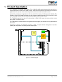
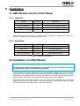
The Embedded I/O Company
TAMC260
PMC-Carrier for AMC
User Manual
Issue 1.0.4
September 2012
TEWS TECHNOLOGIES GmbH
Am Bahnhof 7 25469 Halstenbek, Germany
Phone: +49 (0) 4101 4058 0 Fax: +49 (0) 4101 4058 19
e-mail: [email protected] www.tews.com
TAMC260-10R
Full-Size PMC-Carrier for AMC, 5V PMC I/O
Signaling Voltage
TAMC260-11R
Full-Size PMC-Carrier for AMC, 3.3V PMC I/O
Signaling Voltage
TAMC260-20R
Mid-Size PMC-Carrier for AMC, 5V PMC I/O
Signaling Voltage
TAMC260-21R
Mid-Size PMC-Carrier for AMC, 3.3V PMC I/O
Signaling Voltage
This document contains information, which is
proprietary to TEWS TECHNOLOGIES GmbH. Any
reproduction without written permission is forbidden.
TEWS TECHNOLOGIES GmbH has made any
effort to ensure that this manual is accurate and
complete. However TEWS TECHNOLOGIES GmbH
reserves the right to change the product described
in this document at any time without notice.
TEWS TECHNOLOGIES GmbH is not liable for any
damage arising out of the application or use of the
device described herein.
Style Conventions
Hexadecimal characters are specified with prefix 0x,
i.e. 0x029E (that means hexadecimal value 029E).
For signals on hardware products, an ‚Active Low’ is
represented by the signal name with # following, i.e.
IP_RESET#.
Access terms are described as:
W
Write Only
R
Read Only
R/W
Read/Write
R/C
Read/Clear
R/S
Read/Set
©2012 by TEWS TECHNOLOGIES GmbH
All trademarks mentioned are property of their respective owners.
TAMC260 User Manual Issue 1.0.4
Page 2 of 25
Issue
Description
Date
1.0.0
Initial Issue
May 2009
1.0.1
New Board Revision, added „Handling and Operation
Instructions”
July 2009
1.0.2
Added -2x Variants (Mid-Size Front Panel)
added “TAMC260 Mid-Size Option Usage Restrictions”
added “8.4 Component Height Violation on TAMC260-2x”
November 2011
1.0.3
Only available in RoHS-compliant version
December 2011
1.0.4
Expanded Table 7-1 to cover PMC suitability
added “FRU Data Multi Records”
September 2012
TAMC260 User Manual Issue 1.0.4
Page 3 of 25
Table of Contents
1
2
3
PRODUCT DESCRIPTION ......................................................................................... 6
TECHNICAL SPECIFICATION................................................................................... 7
HANDLING AND OPERATION INSTRUCTIONS ...................................................... 8
3.1
3.2
3.3
3.4
4
ESD Protection ................................................................................................................................8
PCI Bus Signaling Voltage .............................................................................................................8
Voltage Limits on PMCs .................................................................................................................8
TAMC260 Mid-Size Option Usage Restrictions............................................................................8
PEX8112 TARGET CHIP............................................................................................ 9
4.1 PCI Express Configuration Space Register Mapping .................................................................9
4.1.1 PCI-Compatible Configuration Registers (Type 1) ..............................................................9
4.1.2 PCI-Compatible Capability Registers.................................................................................10
4.2 PCI Bus Device Number Mapping ...............................................................................................11
4.3 PCI Clock .......................................................................................................................................11
5
CONFIGURATION HINTS ........................................................................................ 11
5.1 PEX8112Configuration EEPROM.................................................................................................11
6
MODULE MANAGEMENT ....................................................................................... 12
6.1 Indicators .......................................................................................................................................12
6.1.1 On Board Link-LED ............................................................................................................12
6.1.2 Front Panel LEDs...............................................................................................................12
6.2 Temperature and Voltage Sensors..............................................................................................12
6.3 FRU Data Multi-Records ...............................................................................................................13
6.3.1 Connectivity Record ...........................................................................................................13
6.3.2 Module Current Requirement Record ................................................................................13
6.3.3 Clock Configuration Record ...............................................................................................13
7
PMC TO PCI INTERFACE........................................................................................ 14
7.1 PCI Signaling Voltage ...................................................................................................................14
7.1.1 PCI Bus Signal Voltage Level ............................................................................................15
7.1.2 PCI Signaling Levels and Voltage Keying..........................................................................15
8
INSTALLATION........................................................................................................ 17
8.1 AMC Module Insertion & Hot-Swap.............................................................................................17
8.1.1 Insertion .............................................................................................................................17
8.1.2 Extraction ...........................................................................................................................17
8.2 Installation of a PMC Module .......................................................................................................17
8.3 Voltage Limits on PMC Modules .................................................................................................18
8.4 Component Height Violation on TAMC260-2x ...........................................................................19
9
PIN ASSIGNMENT ................................................................................................... 20
9.1
9.2
9.3
9.4
9.5
Overview ........................................................................................................................................20
PMC J11 / P11................................................................................................................................21
PMC J12 / P12 and J22 / P22........................................................................................................22
PMC J14 / P14................................................................................................................................23
Front Panel I/O Connector X1 ......................................................................................................24
TAMC260 User Manual Issue 1.0.4
Page 4 of 25
List of Figures
FIGURE 1-1 : BLOCK DIAGRAM.......................................................................................................................6
FIGURE 7-1 : PCI SIGNAL VOLTAGE CONFIGURATION RESISTORS (BOTTOM VIEW) ..........................15
FIGURE 7-2 : PMC VOLTAGE KEYING ..........................................................................................................16
FIGURE 8-1 : INSTALLATION OF A PMC MODULE ......................................................................................18
FIGURE 8-2 : COMPONENT HEIGHT VIOLATION ACCORDING TO AMC.0 ...............................................19
FIGURE 8-3 : COMPONENT HEIGHT VIOLATION ACCORDING TO MTCA.4.............................................19
FIGURE 9-1 : CONNECTOR OVERVIEW .......................................................................................................20
FIGURE 9-2 : FRONT PANEL I/O CONNECTOR NUMBERING ....................................................................24
List of Tables
TABLE 2-1 : TECHNICAL SPECIFICATION......................................................................................................7
TABLE 4-1 : PCI-COMPATIBLE CONFIGURATION REGISTERS (TYPE 1) ...................................................9
TABLE 4-2 : PCI-COMPATIBLE CAPABILITY REGISTERS...........................................................................10
TABLE 4-3 : PCI BUS DEVICE NUMBER MAPPING......................................................................................11
TABLE 6-1 : ON BOARD LINK-LED ................................................................................................................12
TABLE 6-2 : FRONT PANEL LEDS .................................................................................................................12
TABLE 6-3 : TEMPERATURE AND VOLTAGE SENSORS ............................................................................12
TABLE 7-1 : TAMC260 PCI SIGNALING VOLTAGE FACTORY DEFAULTS.................................................14
TABLE 7-2 : PCI SIGNAL VOLTAGE CONFIGURATION RESISTORS MATRIX...........................................15
TABLE 7-3 : PCI SIGNAL VOLTAGE CONFIGURATION MATRIX.................................................................16
TABLE 8-1 : AMC MODULE INSERTION........................................................................................................17
TABLE 8-2 : AMC MODULE EXTRACTION ....................................................................................................17
TABLE 8-3 : VOLTAGE LIMITS .......................................................................................................................18
TABLE 9-1 : PMC J11/P11 AND J21/P21 PIN ASSIGNMENT........................................................................21
TABLE 9-2 : PMC J12/P12 AND J22/P22 PIN ASSIGNMENT........................................................................22
TABLE 9-3 : PMC J14/P14 PIN ASSIGNMENT...............................................................................................23
TABLE 9-4 : X1 PIN ASSIGNMENT.................................................................................................................25
TAMC260 User Manual Issue 1.0.4
Page 5 of 25
1 Product Description
The TAMC260 is a standard double-width, Full- or Mid-Size AMC module that provides one slot for a
single-width PMC module used to build modular, flexible and cost effective I/O solutions for all kinds of
applications like process control, medical systems, telecommunication and traffic control.
32 bit PCI accesses are supported on PCI bus with PCI frequency 33 MHz and also 66 MHz. The
PLX8112 PCIe-to-PCI bridge provides the real connection between primary PCIe link and the PMC
slot. The bridge controls all PCI accesses and the frequency for the PMC access.
The TAMC260 supports front panel I/O, alternatively a HD68 SCSI-V type connector provides access
to the PMC P14 back I/O lines.
The TAMC260 is a versatile solution to upgrade well known legacy I/O solutions to a high performance
form factor.
According to AMC.0, the TAMC260 provides an IPMI compliant Module Management Controller
(MMC) with temperature monitoring and hot-swap support.
MMC
IPMB
PCI Express
to PCI
Bridge
PCIe (x1)
J14
J11
32 bit
66 MHz
AMC Connector
PCI Bus
J12
68 Pin Connector
Power
Supply
Figure 1-1 : Block Diagram
TAMC260 User Manual Issue 1.0.4
Page 6 of 25
2 Technical Specification
AMC Interface
Mechanical Interface
Advanced Mezzanine Card (AMC) Interface confirming to
PICMG® AMC.0 R2.0
-1x: Double-width / Full-Size Module
-2x: Double-width / Mid-Size Module
Electrical Interface
PICMG® AMC.1 R1.0
PCIe single lane (x1) port (AMC.1 Type 1 compliant)
IPMI
IPMI Version
1.5
Front Panel LEDs
Blue Hot-Swap LED
Red Failure Indication LED (LED1)
Green Board OK / PMC Activity LED (LED 2)
On Board Devices
PEX8112 (PLX Technology)
PCI Express to PCI Bridge
PMC Interface
Number of PMC Slots
1
Supported PMC Data Width
32 bit
Supported PCI Clock
Frequency
33 MHz / 66 MHz
PCI I/O Signaling Voltage
5V & 3.3V
PMC I/O Access
Front Panel I/O
P14 Back I/O via front panel connector
Physical Data
Power Requirements
100 mA typical @ +12V DC (Payload Power)
30 mA typical @ +3.3V DC (Management Power)
Additional power is required by PMC modules
Maximum Power for PMC
Modules
2 A typical @ +5V DC
2 A typical @ +3.3V DC
200 mA typical @ +12V DC
200 mA typical @ -12V DC
Temperature Range
Operating
Storage
MTBF
570 000 h
-40°C - +85°C
-40°C - +85°C
MTBF values shown are based on calculation according to MIL-HDBK-217F and
MIL-HDBK-217F Notice 2; Environment: GB 20°C.
The MTBF calculation is based on component FIT rates provided by the
component suppliers. If FIT rates are not available, MIL-HDBK-217F and
MIL-HDBK-217F Notice 2 formulas are used for FIT rate calculation.
Humidity
5 – 95 % non-condensing
Weight
165 g
Table 2-1 : Technical Specification
TAMC260 User Manual Issue 1.0.4
Page 7 of 25
3 Handling and Operation Instructions
3.1 ESD Protection
The TAMC260 is sensitive to static electricity. Packing, unpacking
and all other handling of the TAMC260 has to be done in an ESD/EOS
protected Area.
3.2 PCI Bus Signaling Voltage
Be sure that the TAMC260 PCI bus Signal Voltage configuration
matches the TAMC260 PMC slots keying pin configuration.
If PMC modules are plugged into a PCI environment where the PCI
signaling voltage does not match, damage to the equipment could
occur, voiding product warranties.
Refer to the chapter “PCI Signaling Voltage” for details.
3.3 Voltage Limits on PMCs
The AMC.0 specification limits the voltages on AMC modules. These
limits also apply to mounted PMCs.
Refer to the chapter “Voltage Limits on PMC Modules” for details.
3.4 TAMC260 Mid-Size Option Usage Restrictions
Please note that the Mid-Size module has restrictions to its usage
because of a component height violation. It is within the
responsibility of the user to carefully check if the Mid-Size module
with its component height violation can be used in his system.
Otherwise damage of the TAMC260 or its slot to be used in may
occur!
Refer to the chapter “Component Height Violation on TAMC260-2x”
for details.
TAMC260 User Manual Issue 1.0.4
Page 8 of 25
4 PEX8112 Target Chip
The PLX8112 PCIe-to-PCI bridge provides the real connection between primary PCIe link and the
PMC slot. The bridge controls all PCI accesses and the frequency for the PMC access.
4.1 PCI Express Configuration Space Register Mapping
4.1.1 PCI-Compatible Configuration Registers (Type 1)
PCI
CFG
Register
Address
31
24
23
16
15
8
7
0
0x00
PCI Device ID
PCI Vendor ID
0x04
PCI Status
PCI Command
0x08
0x0C
PCI Class Code
PCI Built-In SelfTest
(Not Supported)
PCI Header Type
0x10
10B5 8112
0010 0000
PCI Device Revision
ID
060400 AA
PCI Cache Line Size
00 01 00 00
PCI Base Address 0
0x14
0x18
Internal PCI Bus
Latency Timer
0000000C
PCI Base Address 1
Secondary Latency
Timer
Subordinate Bus
Number
Read after
initialization
write access
00000000
Secondary Bus
Number
Primary Bus Number
00 00 00 00
I/O Limit
I/O Base
0220 00 00
0x1C
Secondary Status
0x20
Memory Limit
Memory Base
0000 0000
0x24
Prefetchable Memory Limit
Prefetchable Memory Base
0000 0000
0x28
Prefetchable Memory Base Upper 32 Bits
0x2C
0x30
Prefetchable Memory Limit Upper 32 Bits
I/O Limit Upper 16 Bits
0x34
0x38
0x3C
00000000
00000000
I/O Base Upper 16 Bits
Reserved
0000 0000
PCI Capabilities
Pointer
000000 40
Internal PCI
Interrupt Line
0000 01 00
PCI Base Address for Expansion ROM (Not Supported)
Bridge Control
Internal PCI
Interrupt Wire
Table 4-1 : PCI-Compatible Configuration Registers (Type 1)
TAMC260 User Manual Issue 1.0.4
Page 9 of 25
4.1.2 PCI-Compatible Capability Registers
PCI
CFG
Register
Address
0x40
0x44
31
24
23
16
Power Management Capabilities
Power Management
Data
15
8
Power Management
Next Capability
Pointer
Power Management
Bridge Support
0x48
Device-Specific Control
Reserved
Message Signaled Interrupts Control
0x54
0x58
6A02 5001
00 00 0000
0000 0000
0000 0000
Message Signaled
Interrupts Next
Capability Pointer
Message Signaled
Interrupts Capability
ID
0080 60 05
0000 0000
Message Signaled Interrupts Upper Address
0000 0000
Reserved
0x60
PCI Express Capabilities
Message Signaled Interrupts Data
0x64
PCI Express Next
Capability Pointer
PCI Express
Capability ID
Device Capabilities
PCI Express Device Status
0x6C
0x70
Power Management
Capability ID
Read after
initialization
write access
Message Signaled Interrupts Address
0x5C
0x68
0
Power Management Control/Status
0x4C
0x50
7
0071 00 10
0000 0000
PCI Express Device Control
Link Capabilities
Link Status
0x74
0000 0000
0000 2000
0002 4C11
Link Control
Slot Capabilities
0011 0000
0000 0C80
0x78
Slot Status
Slot Control
0x7C
Reserved
Root Control
0400 0000
0000 0000
0x80
Root Status
0000 0000
0x84
Main Control Register Index
0000 0000
0x88
Main Control Register Data
0000 0000
Table 4-2 : PCI-Compatible Capability Registers
TAMC260 User Manual Issue 1.0.4
Page 10 of 25
4.2 PCI Bus Device Number Mapping
The PCI bus device number of the PMC slot is defined by configuration type translation of the
PEX8112 PCI-Express to PCI Bridge.
By default PMC slot 1 is mapped to bus device number 0x04.
PCI Bus
Device
Number
(HEX)
PCI Bus AD(31:16)
(Binary)
PCI AD
Line used
as PMC
IDSEL
0
0000 0000 0000 0001
16
1–3
0000 0000 0000 0010
…
0000 0000 0000 1000
17 – 19
4
0000 0000 0001 0000
20
5–F
0000 0000 0010 0000
…
1000 0000 0000 0000
21 – 31
10 – 1E
0000 0000 0000 0000
None
1F
Special Cycle Data
-
Purpose
Default IDSEL for
PMC1
Not used on TAMC260
Optional IDSEL for
PMC1
Not used on TAMC260
Not implemented by
PCI-Express to PCI
bridge
Special Cycles for
PMC
Table 4-3 : PCI Bus Device Number Mapping
4.3 PCI Clock
The PCI bus clock on the TAMC260 is configured by the plugged PMC modules. The TAMC260
supports 66MHz PCI bus clock. If the plugged PMC module does only support 33 MHz operation, the
PCI bus will always operate with 33 MHz only.
5 Configuration Hints
5.1 PEX8112Configuration EEPROM
After power-on or PCI reset, the PEX8112 loads initial configuration register data from an on board
configuration EEPROM. Only register values differing from default values are stored in the EEPROM.
For further information please refer to the PEX8112 manual.
Modifications are:
• Address Stepping is disabled (PCI Command Register)
• Slot Clock Configuration is enabled (Link Status/Control Register)
• PCI Express Enable (Device Initialization Register)
TAMC260 User Manual Issue 1.0.4
Page 11 of 25
6 Module Management
6.1 Indicators
For a quick visual inspection the TAMC260 offers 3 LEDs in the front panel and one on board LED.
6.1.1 On Board Link-LED
To help diagnose system bring up problems, the Link Up status of the PEX8112 can be visually
inspected with an on board LED.
LED
Color
State
Description
Link
Red
Off
Link
On
No Link
Table 6-1 : On Board Link-LED
6.1.2 Front Panel LEDs
LED
Color
State
Description
HS
Blue
Off
No Power or module is powered
Short Blink
Hot-Swap negotiation (extraction)
Long Blink
Hot-Swap negotiation (insertion)
On
Module is ready to be powered or module
is ready to be unpowered
Off
No fault
On
Failure or out of service status
Off
Board is unpowered
On
Board is powered
Blink
PMC activity
FAIL
Red
PMC
Green
Table 6-2 : Front Panel LEDs
6.2 Temperature and Voltage Sensors
Sensor Number
Signal Type
Signal Monitored
0
Event
Hot-swap switch
1
Temperature
LM75 #1
2
Temperature
LM75 #2
3
Voltage
+12V (PWR)
4
Voltage
+1.5V
5
Voltage
+12V (PMC)
6
Voltage
-12V (PMC)
Table 6-3 : Temperature and Voltage Sensors
TAMC260 User Manual Issue 1.0.4
Page 12 of 25
6.3 FRU Data Multi-Records
6.3.1 Connectivity Record
The TAMC260 provides a single x1 2.5 Gbps PCI-Express Link on AMC Port 4. The PCI-Express
Interface works with SSC and non SSC PCI-Express Reference Clocks.
6.3.2 Module Current Requirement Record
The TAMC260 FRU data provides the following Module Current Requirement record setting: 2.2A.
6.3.3 Clock Configuration Record
The TAMC260 FRU data provides a clock configuration record for FCLKA. FCLKA is a PCI Express
Gen 1 clock receiver without PLL activated by the carrier and with a nominal clock frequency of
100 MHz.
TAMC260 User Manual Issue 1.0.4
Page 13 of 25
7 PMC to PCI Interface
7.1 PCI Signaling Voltage
PMC modules are specified for 3.3V only, 5V only, or universal (3.3V or 5V) PCI signal voltage
operation.
The TAMC260 on board S_V/IO signal voltage level defines the PCI signal voltage level for the
TAMC260 PCI bus. A voltage key pin indicates the PCI signal voltage and prevents PMCs with a
wrong signaling voltage from being plugged onto the carrier.
PMC PCI Signaling Voltage
TAMC260
S_V/IO
Configuration
5V Keying Pin
Configuration
3.3V Keying
Pin
Configuration
5V only
PMC
-x0
5V
Installed
Not Installed
9
9
8
-x1
3.3V
Not Installed
Installed
8
9
9
Universal 3.3V only
PMC
PMC
Table 7-1 : TAMC260 PCI Signaling Voltage Factory Defaults
WARNING!!!
Be sure that the TAMC260 PCI bus Signal Voltage (S_V/IO) configuration matches the TAMC260
PMC slots keying pin configuration.
Be sure that the used PMC modules match to the TAMC260 PCI bus Signal Voltage and PMC
slot keying pin configuration.
If PMC modules are plugged into a PCI environment where the PCI signaling voltage does not
match, damage to the equipment could occur, voiding product warranties.
TAMC260 User Manual Issue 1.0.4
Page 14 of 25
7.1.1 PCI Bus Signal Voltage Level
The S_V/IO signal voltage level is configured on board with three resistors. To change the S_V/IO
voltage level, these resistors must be soldered to the appropriate soldering terminals. These reside on
the bottom side of the TAMC260 and are grouped with a copper frame.
Figure 7-1 : PCI Signal Voltage Configuration Resistors (Bottom View)
TAMC260 S_V/IO
Configuration
Populated
Resistors
Unpopulated
Resistors
5V
R88, R89, R90
R85, R86, R87
3.3V
R85, R86, R87
R88, R89, R90
Table 7-2 : PCI Signal Voltage Configuration Resistors Matrix
7.1.2 PCI Signaling Levels and Voltage Keying
To prevent a PMC from being plugged into a PMC system with a different PCI signaling voltage, the
PMC specification defines voltage keying with keying pins (on the PMC carrier board) and keying
holes (on the PMC module).
PMC cards that only support 5 Volt PCI signaling voltage provide a single keying hole for the 5 Volt
keying pin. A 3.3 Volt only PMC provides only the keying hole for the 3.3 Volt keying pin. Universal
PMC cards, which can handle 3.3 Volt and 5 Volt PCI signaling voltage, have keying holes for both
voltage keying pins.
In certain system configurations it may be necessary to remove the keying pin from one location and
assemble it at the other keying pin location.
TAMC260 User Manual Issue 1.0.4
Page 15 of 25
Figure 7-2 : PMC Voltage Keying
Use the following table to identify the required TAMC260 voltage keying for the actual PMC modules
that are to be used.
PMC
PCI Signal
Voltage
Capability
TAMC260
S_V/IO
Configuration
3.3V Only
3.3V
Not Installed
Installed
3.3V
Not Installed
Installed
5V
Installed
Not Installed
5V
Installed
Not Installed
3.3V or 5V
5V Only
TAMC260 5V TAMC260 3.3V
Keying Pin
Keying Pin
Configuration Configuration
Table 7-3 : PCI Signal Voltage Configuration Matrix
TAMC260 User Manual Issue 1.0.4
Page 16 of 25
8 Installation
8.1 AMC Module Insertion & Hot-Swap
8.1.1 Insertion
Handle
Blue LED
Description
Open (Full extracted)
OFF
Insert Module into slot
Open (Full extracted)
ON
Module is ready to attempt activation
Closed (Pushed all way in)
Long Blink
Hot-Swap Negotiation
Closed (Pushed all way in)
OFF
Module is ready & powered
Table 8-1 : AMC Module Insertion
When the blue LED does not go off, but returns to the “ON” state, the module FRU information is
invalid or the carrier cannot provide the necessary power.
8.1.2 Extraction
Handle
Blue LED
Description
Pulled out 1/2
OFF
Request Hot-Swap
Pulled out 1/2
Short Blink
Hot-Swap Negotiation
Pulled out 1/2
ON
Module is ready to be extracted
Open (Full extracted)
ON
Extract Module from slot
Table 8-2 : AMC Module Extraction
8.2 Installation of a PMC Module
Before installing a PMC module, be sure that the power supply for the TAMC260 is turned off.
The components are Electrostatic Sensitive Devices (ESD). Use an anti-static mat connected to
a wristband when handling or installing the components.
If the PMC has a front panel, remove the cover from the PMC front panel cut-out of the TAMC260.
Install the PMC at an angle so that the PMC front panel penetrates the PMC front panel cut-out. Then
rotate down to mate with the PMC connectors on the TAMC260. If the PMC has no front panel, simply
plug in the PMC, and leave the cover in the PMC front panel cut-out of the TAMC260.
After the PMC module has been installed, it can be mounted on the TAMC260 using the mounting
screws that come with the PMC module. There are four screw mounting locations, two at the PMC
front panel and two at the standoffs near the PMC bus connectors.
TAMC260 User Manual Issue 1.0.4
Page 17 of 25
Figure 8-1 : Installation of a PMC Module
WARNING!!!
Be sure that the TAMC260 PCI bus Signal Voltage (S_V/IO) configuration matches the TAMC260
PMC slots keying pin configuration.
Be sure that the used PMC modules match to the TAMC260 PCI bus Signal Voltage and PMC
slot keying pin configuration.
If PMC modules are plugged into a PCI environment where the PCI signaling voltage does not
match, damage to the equipment could occur, voiding product warranties.
8.3 Voltage Limits on PMC Modules
The AMC.0 specification limits the voltages on AMC modules to following thresholds:
DC voltage
AC voltage
Positive
+27V
+27V peak
Negative
-15V
-15V peak
Table 8-3 : Voltage Limits
For PMC modules using voltages (including I/O voltages) that exceed these thresholds, an additional
insulation to adjacent modules or carrier boards becomes necessary.
TAMC260 User Manual Issue 1.0.4
Page 18 of 25
8.4 Component Height Violation on TAMC260-2x
With an assembled standard PMC module the Mid-Size TAMC260-2x violates the AMC component
envelope as defined in AMC.0. The picture shows in red the violation of the hatched AMC component
envelope.
Envelope 1
0,64 mm
Envelope 2
0,29 mm
1,65 mm
Envelope 3
2,65 mm
Figure 8-2 : Component Height Violation according to AMC.0
When using the TAMC260-2x on an AdvancedTCA carrier, it is within the responsibility of the user to
carefully check if the Mid-Size module with its component height violation can be used. Otherwise
damage of the TAMC260 or the carrier may occur!
MTCA.0, although the adjacent board is also an AMC, maintains the steps in the Mid-Size AMC
component envelope, which were originally defined in AMC.0 to provide spacing for components on
ATCA carrier boards.
MTCA.4 removes the steps in the Mid-Size AMC component envelope. This results in a reduced
component height violation if the TAMC260-2x is used in MTCA.4 systems.
0,64 mm
0,29 mm
Figure 8-3 : Component Height Violation according to MTCA.4
The TAMC260-2x is intended for the use in µTCA systems because the adjacent AMC module
provides enough spacing for the protruding PMC module. Despite the fact that the AMCs component
envelope is violated by the PMC, the PMC does not cross the interboard separation plane, and a
minimum distance between the PMC and the adjacent AMC is guaranteed. This allows improving the
density of the µTCA system.
If you are not sure if the available spacing is sufficient, it is strongly recommended to use the Full-Size
TAMC260-1x. It is within the responsibility of the user to carefully check if the Mid-Size module with its
component height violation can be used in his system. Otherwise damage of the TAMC260 or its slot
to be used in may occur!
TAMC260 User Manual Issue 1.0.4
Page 19 of 25
9 Pin Assignment
9.1 Overview
Figure 9-1 : Connector Overview
J1, J2 and J3 are for factory use only.
TAMC260 User Manual Issue 1.0.4
Page 20 of 25
9.2 PMC J11 / P11
Pin
Signal
Signal
Pin
1
TCK
-12V
2
3
GND
INTA#
4
5
INTB#
INTC#
6
7
BUSMODE1#
+5V
8
9
INTD#
PCI-RSVD
10
11
GND
3.3Vaux
12
13
CLK
GND
14
15
GND
GNT#
16
17
REG#
+5V
18
19
V (I/O)
AD[31]
20
21
AD[28]
AD[27]
22
23
AD[25]
GND
24
25
GND
C/BE[3]#
26
27
AD[22]
AD[21]
28
29
AD[19]
+5V
30
31
V (I/O)
AD[17]
32
33
FRAME#
GND
34
35
GND
IRDY#
36
37
DEVSEL#
+5V
38
39
GND
LOCK#
40
41
PCI-RSVD
PCI-RSVD
42
43
PAR
GND
44
45
V (I/O)
AD[15]
46
47
AD[12]
AD[11]
48
49
AD[09]
+5V
50
51
GND
C/BE[0]#
52
53
AD[06]
AD[05]
54
55
AD[04]
GND
56
57
V (I/O)
AD[03]
58
59
AD[02]
AD[01]
60
61
AD[00]
+5V
62
63
GND
REQ64#
64
Table 9-1 : PMC J11/P11 and J21/P21 Pin Assignment
TAMC260 User Manual Issue 1.0.4
Page 21 of 25
9.3 PMC J12 / P12 and J22 / P22
Pin
Signal
Signal
Pin
1
+12V
TRST#
2
3
TMS
TDO
4
5
TDI
GND
6
7
GND
PCI-RSVD
8
9
PCI-RSVD
PCI-RSVD
10
11
BUSMODE2#
+3.3V
12
13
RST#
BUSMODE3#
14
15
+3.3V
BUSMODE4#
16
17
PME#
GND
18
19
AD[30]
AD[29]
20
21
GND
AD[26]
22
23
AD[24]
+3.3V
24
25
IDSEL
AD[23]
26
27
+3.3V
AD[20]
28
29
AD[18]
GND
30
31
AD[16]
C/BE[2]#
32
33
GND
PMC-RSVD
34
35
TRDY#
+3.3V
36
37
GND
STOP#
38
39
PERR#
GND
40
41
+3.3V
SERR#
42
43
C/BE[1]#
GND
44
45
AD[14]
AD[13]
46
47
M66EN
AD[10]
48
49
AD[08]
+3.3V
50
51
AD[07]
PMC-RSVD
52
53
+3.3V
PMC-RSVD
54
55
PMC-RSVD
GND
56
57
PMC-RSVD
PMC-RSVD
58
59
GND
PMC-RSVD
60
61
ACK64#
+3.3V
62
63
GND
PMC-RSVD
64
Table 9-2 : PMC J12/P12 and J22/P22 Pin Assignment
TAMC260 User Manual Issue 1.0.4
Page 22 of 25
9.4 PMC J14 / P14
The PMC J14 / P14 I/O connector routes the PMC I/O lines directly to the appropriate pins of the
SCSI-V (VHDCI/Champ) receptacle type cable connector. The actual signal assignment of the PMC
J14 / P14 connector is PMC specific.
Pin
Signal
Signal
Pin
1
I/O 1
I/O 2
2
3
I/O 3
I/O 4
4
5
I/O 5
I/O 6
6
7
I/O 7
I/O 8
8
9
I/O 9
I/O 10
10
11
I/O 11
I/O 12
12
13
I/O 13
I/O 14
14
15
I/O 15
I/O 16
16
17
I/O 17
I/O 18
18
19
I/O 19
I/O 20
20
21
I/O 21
I/O 22
22
23
I/O 23
I/O 24
24
25
I/O 25
I/O 26
26
27
I/O 27
I/O 28
28
29
I/O 29
I/O 30
30
31
I/O 31
I/O 32
32
33
I/O 33
I/O 34
34
35
I/O 35
I/O 36
36
37
I/O 37
I/O 38
38
39
I/O 39
I/O 40
40
41
I/O 41
I/O 42
42
43
I/O 43
I/O 44
44
45
I/O 45
I/O 46
46
47
I/O 47
I/O 48
48
49
I/O 49
I/O 50
50
51
I/O 51
I/O 52
52
53
I/O 53
I/O 54
54
55
I/O 55
I/O 56
56
57
I/O 57
I/O 58
58
59
I/O 59
I/O 60
60
61
I/O 61
I/O 62
62
63
I/O 63
I/O 64
64
Table 9-3 : PMC J14/P14 Pin Assignment
TAMC260 User Manual Issue 1.0.4
Page 23 of 25
9.5 Front Panel I/O Connector X1
SCSI-V (VHDCI/Champ) receptacle, HDRA-EC68LFDT-SL+ or compatible.
34
1
FAIL
X1
TAMC260
PMC
68
35
Figure 9-2 : Front Panel I/O Connector Numbering
The PMC J14 / P14 I/O connector routes the PMC I/O lines directly to the appropriate pins of the
SCSI-V (VHDCI/Champ) receptacle type cable connector. The actual signal assignment of the PMC
J14 / P14 connector is PMC specific.
TAMC260 User Manual Issue 1.0.4
Page 24 of 25
Pin
Signal
Signal
Pin
1
I/O 1
I/O 2
2
3
I/O 3
I/O 4
4
5
I/O 5
I/O 6
6
7
I/O 7
I/O 8
8
9
I/O 9
I/O 10
10
11
I/O 11
I/O 12
12
13
I/O 13
I/O 14
14
15
I/O 15
I/O 16
16
17
I/O 17
I/O 18
18
19
I/O 19
I/O 20
20
21
I/O 21
I/O 22
22
23
I/O 23
I/O 24
24
25
I/O 25
I/O 26
26
27
I/O 27
I/O 28
28
29
I/O 29
I/O 30
30
31
I/O 31
I/O 32
32
33
I/O 33
I/O 34
34
35
I/O 35
I/O 36
36
37
I/O 37
I/O 38
38
39
I/O 39
I/O 40
40
41
I/O 41
I/O 42
42
43
I/O 43
I/O 44
44
45
I/O 45
I/O 46
46
47
I/O 47
I/O 48
48
49
I/O 49
I/O 50
50
51
I/O 51
I/O 52
52
53
I/O 53
I/O 54
54
55
I/O 55
I/O 56
56
57
I/O 57
I/O 58
58
59
I/O 59
I/O 60
60
61
I/O 61
I/O 62
62
63
I/O 63
I/O 64
64
65
GND
GND
66
67
GND
GND
68
Table 9-4 : X1 Pin Assignment
TAMC260 User Manual Issue 1.0.4
Page 25 of 25