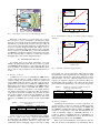
1
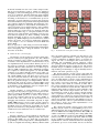
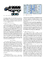
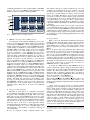
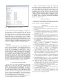
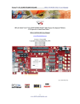
Hardware/software debugging of large scale
many-core architectures
Stephanie Friederich, Jan Heisswolf, Jürgen Becker
Karlsruhe Institute of Technology
Karlsruhe, Germany
Email: [email protected]
Abstract—The size of current multi-processor system-on-chip
(MPSoC) is growing unsustainable. Besides, new decentralized
software approaches are being developed to handle the management of increasing resources. To verify the system functionality
of these novel hardware/software systems, sufficiently accurate
models are required. However, current simulation tools have
limited scalability and performance; hence hardware prototypes
and debugging concepts are necessary for system verification.
We present a novel debug approach which offers visualization of
hardware/software interaction for system level verification. The
debug concept comprises debug probes within each router of
the network as well as monitoring units to trace the activity of
each core in the MPSoC. In addition a transactor based method
is proposed to transmit the huge amount of debug information
out of the hardware prototype to evaluate the information on
a standard host computer. Experimental results show that the
resource overhead is insignificant in contrast to the gain of
extensive debug possibilities. Furthermore the number of pins
required for the presented debugging concept is kept constant
independent of the architecture size and thus we are not facing
problems of limited debug interfaces or pins. In comparison to
conventional debugging we show improvements in scalability and
bandwidth.
I.
I NTRODUCTION
One of the challenges in modern multi-core system design
is the connection of prototyping platforms into system-onchip (SoC) modeling environments. The development of new
hardware requires early system debugging and verification
methods, but due to system complexity this task gets more
and more complicated. To accelerate the overall multi-core
SoC design development process, early software development
is one of the crucial factors but only possible if simulation
models or a prototype of the system is available. Because
register-transfer level (RTL) simulation is too slow for designs
consisting of millions of transistors, prototyping on a fieldprogrammable gate array (FPGA) platform is one way to speed
up the development process of new hardware architectures.
But the implementation of the design in hardware leads to
new problems. Restricted hardware resources, such as limited
memory and gates lead to restricted size of the design under
test. In addition due to lack of physical interfaces the debug
possibilities are also constricted.
Another challenge is to verify both the logic of the hardware
design as well as the embedded software. The hardware design
contains multiple processors, different memory systems and
complex interfaces. To speed up the development of operating
systems and software drivers it is necessary to have a working
prototype of the hardware design as soon as possible. Having
such a hardware prototype it is then possible to boot the
operating system and validate that the software runs properly.
But one question arises here, how do we get the software into
our system and execute the software?
FPGA prototyping is widely used in semiconductor design.
The verification of simple and small designs could be made
with common FPGA evaluation boards. If it comes to bigger
designs prototyping platforms with multiple FPGAs are used.
In case of this paper we are using the CHIPit prototyping
platform from Synopsys, which includes six Virtex5 FPGAs.
Common rapid SoC FPGA-based prototyping hardware platforms like Haps 70 series from Synopsys [1] and V7 TAI
Logic Module from S2C [2], as well as the CHIPit system, do
not have many interfaces. Even custom designed prototyping
platforms are not capable to provide as many interfaces as a
multi-processor design with hundreds of cores would require.
Hence it would not be possible to debug all processors on core
level.
Previous debug modules did not give the possibility to trace the
processor instructions as well as the network communication.
The Gaisler LEON system originally did not include a NoC
system and hence one connection for the debug support unit
was sufficient. Novel tile based NoC systems require more than
one debug support units and therefore it is hardly possible to
connect every unit with one physical interface. The Universal
Multi-Resource Bus (UMRbus) based approach allows to have
as many interfaces in the design as we want.
The paper is organized as follows: the following section describes related work on NoC debugging techniques, extending
the number of debug interfaces, and a multi-core hardware
architecture which was used in the following sections. Section
three describes the implementation of the transactor and the
integration into the debug unit as well as the debug extension
of the router. The experimental results are presented in section
four. The last section presents a forecast of upcoming work.
II.
R ELATED WORK
To enable core level debugging, several debug interfaces
are required within the network. With huge NoC sizes, available interfaces on common FPGA development boards are not
sufficient anymore and hence other solutions to increase the
number of debug interfaces need to be found. This section first
describes conventional network debugging methods and then
techniques to increase the number of interfaces are presented.
A. NoC debugging techniques
The observation of the communication within a NoC-based
architecture is crucial for different reasons: (1) tuning and
debugging of applications, (2) identification of bottlenecks /
system debugging, (3) analysis of deadlock situations and (4)
debugging of the communication hardware. Different monitoring concepts for NoC-based architectures have been proposed
in the past, most of all to observe the network communication:
In [3] a concept for system-level and application debugging
was introduced. It uses monitoring probes that model the
monitored information in the form of time stamped events.
The proposed monitoring system is suitable for application
debugging (1) and system debugging (2). Low level debugging
(3+4) is not addressed. Another monitoring design template
is presented in [4]. It can be used for performance analysis
and debug of the interactions of a embedded NoC processors
architecture. A generic template for bus and router monitoring
is introduced. However, the presented monitoring infrastructure
only comprises -high level debugging and monitoring (1+2).
Debugging and analysis of early software and hardware prototypes necessitates a more detailed analysis of the communication. Deadlock situations might occur and need then to be
analyzed. There are several reasons for deadlocks, ether they
result from hardware bugs or conceptual weaknesses in the
software layers. Such detailed observability (3+4) have not
been addressed explicitly yet. Time consuming conventional
hardware debugging by the use of logic analyzers or FPGA
analyzers (e.g. Xilinx ChipScope) were often used for detailed
analysis. In contrast, our concept for detailed NoC debugging
is very simple to use. It is detailed in Section III-E1 and
Section III-D.
In [5] an approach to online debug for NoC-based multiprocessor SoCs is introduced. The described debug infrastructure
allows investigating and to debug the behavior of an NoCbased SoC at run-time.
B. Virtual interfaces for debugging
Growing NoC systems require more and more debug interfaces but common prototyping platforms only offer a limited
amount of interfaces. One possibility to increase the number
of interfaces is the implementation of virtual interfaces, in [6]
one implementation has been described. Thereby all cores of
the system are connected to an Advanced eXtensible Interface
(AXI) bus. The bus is then connected to one core that is responsible for UART communication. All communication with the
host computer is redirected through the core with the UART
connection (it is named embedded virtual server). This core
is connected with the host computer by a conventional serial
line. Virtual UARTs provide each single process access to its
own serial connection. However, this concept only addresses
designs where all processors are connected to the same bus.
Due to the partitioned design over multiple FPGAs, which is
described in this work, the concept of virtual UARTs would
not be feasible. Another drawback of the virtual UART concept
is the limitation of the bandwidth to the host computer due to
the use of a single UART connection.
Another alternative of virtual interfaces is a transactor
based approach. In [7] the prototyping of a heterogeneous multiprocessor system-on-chip (MPSoC) design, which consists of
general purpose RISC processors as well as novel accelerators in form of tightly-coupled processor arrays (TCPA), is
described. The focus of this work was the transactor based
debugging and verification of the TCPA component. A single
AMBA AHB transactor is used to realize one data connection
between software running on a host PC and the hardware on
the FPGA board. As described in section III-C we use this
approach and extend it by using multiple transactors, since a
scalable NoC based architecture was not considered yet.
C. Invasive computing
Invasive computing is a novel paradigm for designing and
programming future parallel computing systems. For systems
with more than 1000 cores on a single chip, resource-aware
programming is of utmost importance to obtain high utilization
as well as computational and energy efficiency numbers. With
CPU
CPU
CPU
CPU
CPU
CPU
CPU
CPU
CPU
CPU
CPU
CPU
Memory
i-NoC
Router
Memory
i-NoC
Router
CPU
Memory
i-NoC
Router
CPU
Memory
CPU
CPU
and
CPU
CPU
CPU
CPU
I/O
Memory
i-NoC
Router
Memory
i-NoC
Router
CPU
CPU
CPU
CPU
CPU
CPU
CPU
CPU
CPU
CPU
CPU
CPU
Memory
i-NoC
Router
Fig. 1.
i-NoC
Router
Memory
Memory
i-NoC
Router
i-NoC
Router
InvasIC Network on Chip (NoC) hardware architecture
this goal in mind, invasive computing was introduced to give
a programmer explicit handles to specify and argue about
resource requirements in different phases of execution. To
support this idea of self-adaptive and resource-aware programming, new programming concepts, languages, compilers, operating systems, and hardware architectures have been
developed within the invasive research project. The invasive
hardware design of a MPSoC (multiprocessor systems-on-achip) includes profound changes to support efficiently invasion,
infection, and retreat operations. [8], [9]
The invasive Network on Chip (i-NoC) [10] builds the
communication infrastructure of the InvasIC architecture. It is
a wormhole packet switching network with Virtual Channels
(VCs) providing Quality of Service (QoS) communication by
the use of end-to-end connections as detailed in [11]. The iNoC consists of two basic components - the network adapter
(NA) and the routers which are connected via links. The iNoC routers [12] build a meshed topology and are responsible
for the data transmission between the tiles. Therefore a distributed routing scheme is realized to ensure scalability of the
architecture. The network adapter attaches the i-NoC to the
tile internal bus system. It has a memory mapped interface
and is responsible for transparent fetching of data from tile
external memories, generation of special system messages and
management of the i-NoC features. The tiles itself could be of
various types. Simple compute tiles with multiple processors,
memory and IO tiles, and also special hardware accelerator
tiles. Figure 1 shows one possible implementation of an
invasive hardware architecture.
The compute tile internal concept is based on the Gaisler
IP library [13]. It consists of several LEON3 processor cores,
different memories and several peripherals all connected to a
tile local AMBA Advanced High-performance Bus (AHB). In
addition each tile has a monitoring and a debug (DSU) unit,
as well as an AHB master transactor. The Ethernet and DDR2
memory controller are optional components, which are added
in case of a Memory and I/O tiles. Figure 2 shows one possible
implementation of the tile architecture. There are many higher
performance, processors on the market, but most of them are
LEON 3
CPU
LEON 3
CPU
LEON 3
CPU
FPU L1
FPU L1
FPU L1
FPU L1
FPU L1
MMU
MMU
MMU
MMU
MMU
L2
Cache
128kB
AHB
Ethernet
(optional)
DDR2
DSU
Controller
(optional) AHB/APB
bridge
Transactor
SRAM Monitor
Controller
(TLM)
APB
UART
Timer
Interrupt
controller
Message
In Port
Proxy 1
Message
In Port
Proxy 3
DUT
Message
In Port 1
Transactor
1
Message
Out Port 2
Message
Out Port
Proxy 2
Software side
Host
workstation
Fig. 3.
Fig. 2.
DUT
Proxy
Testbench
module 1
LEON 3
CPU
Testbench
module 2
Network
adapter
LEON 3
CPU
UMRbus
Message
Out Port
Proxy 4
Message
In Port 3
Message
Out Port 4
Clock/
reset
generation
and
control
Transactor
2
Hardware side
(emulator)
CHIPit Platform
UMRBus transactor model
Single compute tile architecture
not available as HDL source code. Therefore, we decided to
use the LEON3 processors as well as other components of the
Gaisler GRLIB. It is released in open-source under the GNU
GPL license. Since our architecture is built in a modular way,
it is easy to exchange the LEON core with any other processor
core with an AHB interface later.
D. LEON3 processor debug interface
The Aeoroflex Gaisler tool GRMON2 [14] is a general
debug monitor for LEON3 processors, and for SoC designs
based on the GRLIB IP library. The Debug Support Unit
(DSU) provides a non-intrusive debug environment for the
Leon-Cores on real target hardware. The LEON3 DSU can
be controlled through any AMBA AHB master in a systemon-chip design. The debug interface can be of various types:
serial UART, Ethernet or as described in section III-C, also
user defined interfaces can be used. The GRMON2 monitor
interfaces to the on-chip debug support unit (DSU), implementing a large range of debug functions. These functions are for
example upload and execution of LEON applications, built-in
disassembler and trace buffer management, and read and write
access to all system registers and memory which are accessible
in the tile local address range. Since the GRMON2 debug
monitor is intended to debug system-on-chip (SOC) designs
but not network-on-chips (NoC) designs, it is necessary to have
multiple DSU and GRMON2 instances in NoC designs such
as the invasive hardware architecture.
III.
C ONCEPT
The concurrent development of novel hardware and software components requires debugging on several levels to
verify the system functionality. The integration of hardware
components into one design causes errors, even if the single
components have been verified before. Also some errors only
occur during the interaction of hardware and software. To
detect these kind of errors, in detail system level verification
is required, but due to the size and complexity of currents
systems quite comprehensive.
The following section describes on the one hand the concept
of using an AHB master transactor to exchange data between
a software running on the host machine and the hardware
design configured on the FPGAs of the CHIPit system. And
on the other hand the novel NoC based debugging technique
is presented.
A. CHIPit Platinum edition
The CHIPit Platinum Edition System is a high-capacity,
high-speed emulation and rapid prototyping system for ASIC
designs. It contains six Xilinx Virtex-5 LX330T FPGAs which
is equivalent to 12 million ASIC gates; furthermore the platform can be extended up to 18 FPGAs. On the top of the
prototyping system there are extension board interfaces to plug
in up to six extension boards, such as memory, Ethernet and
other interfaces.
In addition to the extension board interfaces, the CHIPit platform is connected to a host computer via the UMRbus (Universal Multi-Resource bus). This bus builds the interconnection
for transactor based communication where hardware running
on the CHIPit FPGAs is connected to software which is
executed on the host computer. The transactor based communication builds the background of the debugging interface which
is described in this paper. The maximum clock frequency of the
FPGA platform is defined to 100MHz, due to the clock latency
between FPGAs. More details about the CHIPit platform and
its use for many-core prototyping are provided in [15].
B. UMRbus AHB master transactor
The Synopsys Transactor Library for AMBA is the link
between AMBA based user designs and the software environment on a PC host machine. The connection between the
AMBA bus on the FPGA side and software running on a host
PC is provided by the UMRbus. With respect to the AMBAbased LEON3 cores that are used in our prototype, these
transactors play an important role as detailed later. The library
packet includes several AMBA transactors, such as master and
slave components for different bus systems, including AHB
and AXI. The library package includes the hardware IP for
each transactor as well as a C++ library; hence the user does
not need to care about the UMRbus implementation. The user
only needs to configure the transactor for its own purpose and
integrate it into the project. For more information about the
Transactor Library see [16].
The UMRbus based transactor model is shown in figure
Figure 3. The left side represents the software part with
multiple software instances and the right side represents the
hardware adapter and the design under test (DUT). In the
middle lies the UMRBus driver which connects the hardware
and software side. Since the communication over the UMRbus
is carried out in a serial way, each transactor includes two
FIFOs to store incoming and outgoing messages. The inport
FIFO holds data packets while the AHB bus fabric processes
them. While the outport FIFO queues the messages while
the UMRbus is busy. Both FIFO sizes could be customized
in the range of 16 to 4095 32-bit words. Figure 4 shows
the connection of the transactor hardware components. Each
component inside one FPGA is connected in a serial way, as
well as the communication between FPGAs and the UMRbus
UMRBus rst
UMRBus
out
FPGA 2
UMRBus
component
9
UMRBus
component
8
FPGA 5
UMRBus
component
6
UMRBus
component
5
UMRBus
component
4
FPGA 1
FPGA 6
Fig. 4.
UMRBus
component
3
UMRBus
component
2
UMRBus clk
UMRBus
component
1
UMRBus
in
UMRbus communication interface
communication interface is also serialized. Hence each FPGA
requires only one set of UMRbus signal independent of the
number of transactor instances inside the FPGA.
FPGA 3
UMRBus
component
7
FPGA 4
UMRBus connection over FPGA boundaries
C. GRMON connection with the AHB transactor
As described in section II-D the LEON3 processor comes
with its own debugging unit (DSU) which can be connected
to the debug tool GRMON2 to access debug information. The
default communication interface between GRMON2 and the
system running on an FPGA is a serial interface connected to
the AHB UART of the target system. Since our prototyping
platform only has two serial interfaces, and it is required
to have a connection to each individual tile, we need to
apply other interfaces to connect GRMON2. In addition to the
supported debug communication interfaces, it is possible to
add a custom interface using a loadable module. The custom
interface only needs to provide functions to read and write
data on the AHB bus, which is equivalent to an AHB master
interface. Hence we are using the AHB master transactors of
the Synopsys transactor library to connect GRMON2 with the
AHB bus on each tile. Only once a loadable module must be
compiled into a shared library which includes read and writes
function as well as an initialization of the transactor. The user
than can start GRMON2 in a common way with the shared
library and the tile ID as parameters. Now it is possible to run
multiple sessions of GRMON2 in parallel, all linked with the
UMRbus. Another advantage of the UMRbus connection, even
with multiple GRMON2 instances, is the much higher data
rate than a system with one serial connection per GRMON
instance. This high data rate improves the usability of the
prototype (e.g. if large binaries are loaded to the architecture).
The GRMON2 connection could also be used to transfer the
monitoring data of the network, which is described in the
following section. Thus there is no need for an additional
interface.
D. Concept for NoC debugging
Especially in early phases of a hardware development
process hardware units might contain bugs that have not been
recognized while simulating the design. Thus, these bugs
make their way into the first FPGA-based prototypes of the
architecture. Such bugs might only show up in case of complex
software scenarios executed on the parallel architecture. Drawing inferences from the erroneous behavior of the software
about the source of the error is often impossible without
detailed investigation. Executing a complex parallel software
on simulated hardware is too time consuming. Thus, realtime debugging of the hardware is required to find bugs in
a reasonable time.
In case of a Network on Chip, a detailed analysis of the
data transfers can help to localize a hardware bug or an error
resulting from an misapplication by the software1 . For such
an analysis the latest data on the NoC need to be analyzed
after an error occurred. Therefore a history of the latest data
needs to be available. This history can be accessed on demand
once an error occurred to analyze what was going on under the
hood triggering the error. For a detailed analysis we propose
one separate history per router port. Thus, a packet will be
captured by multiple debugging histories. This help to localize
a potential hardware bug and gives an indication on the faulty
component.
The debugging history needs to be accessible even when the
cores crashed and cannot be used for software execution anymore. In combination with GRMON2 and the transactor based
communication (see Section III-C) it is possible to access the
memory mapped debug registers directly. More details about
the realization of the NoC debugging infrastructure are given
in Section III-E1.
E. Implementation
Figure 1 shows the implemented architecture with the tile
internal structure shown in figure 2. Since each tile contains
five LEON3 cores, the implemented design comprises 45 cores.
Single FPGAs are too small to enclose the complete design.
Thus we partitioned the design and distributed it over six
FPGAs.
Due to our memory map concept with the same address range
inside each tile, it is necessary to insert one debug support unit
into every tile, thereby we have access to the entire address
space in our system. The CHIPit prototyping system does not
have as many physical interfaces as it is required for inserting
one debug support unit into every tile. Hence we are using the
transactor based approach as described in the previous section.
We include one I/O transactor into every tile on the hardware
side. On the software side on our host PC we connect one
GRMON2 monitor to each transactor.
To connect the AHB transactor with GRMON2 [14] we
created a shared object library, which get the transactor ID as
an input value. To load the module which includes the custom
interface, the shared object library as well as the tile ID to
which we want to build the connection has to be added as
parameters when opening a GRMON2 monitor. The following
shows the command to start GRMON2:
./grmon -dback my io.so -dbackarg Tile ID
After starting GRMON2, the UMRbus interface will be initialized. Afterward data could be read and written to any
memory location which is implemented and accessible through
the AHB bus.
1) NoC debugging implementation: To enable real-time
debugging of the communication of the invasive Network on
Chip, a debug queue is realized at each router input port and
at the local output port, as shown in Figure 5. Each queue is
realized as a shift register that drops the oldest value to store
the latest data. The queues at the input ports help to check the
data arriving from the neighboring routers or from the network
adapter in case of the local port. The additional queue at the
output port helps to check whether data have left the NoC
valid or corrupted. The size s of each queue depends on the
required length of the history that needs to be captured and
can be set at design time. In Section IV-A2 the impact of s
on the resource requirements is investigated.
1 During the development of the i-NoC multiple bugs have been found
by real-time analysis of the communication data. Compared to ChipScope
that was used before, the NoC debug registers improved debugging speed
significantly.
In Ports
Debug Queue
Buffer
Buffer
Buffer
Buffer
Routing
Reservation
Table
Out Ports
Debug Queue
Port 1
Debug Queue
Port N
UMRbus
UART
Virtual UART
103
Buffer
Buffer
Buffer
Buffer
Port 1
102
101
Port N
Transmission
Control
100
21
23
Block diagram of the i-NoC router with debugging extension
Each time a flit arrives at a router input port or leaves
the local port, a copy is forwarded to the respective debug
queue. It is stored in the queue in combination with additional
information (e.g. the ID of the used VC or the type of flit). In
case of an error the latest flits transferred on each link can be
access by a memory mapped interface that enables access to
all entries of the debug queue. This interface is part of the NA
and is connected to the AHB bus to access the information
via GRMON. A dedicated connection between the each router
and the connected NA is realized to forward the requested
debugging data to the memory mapped interface.
IV.
A. Resource overhead
1) AHB transactor overhead: Including the AHB transactor into each tile, there is a small overhead of resources in
contrast of using only serial interfaces. The size of inport and
outport FIFOs inside the transactor module could be custom
parameterized and hence the consumption of BRAM varies.
Table I shows the resource consumption of our AHB transactor
implementation in contrast to an UART. The number of pins
used by one transactor component is also higher than for
one simple serial interfaces, but if more than one transactor
component is placed into one FPGA, they all share the same
pin resources. Figure 6 shows the pin utilization, in terms
of different number of tiles, for implementation with serial
interfaces, our UMRbus based concept, and the virtual UART
[6].
TABLE I.
D ESIGN SPACE EXPLORATION OF DEBUGGING
ALTERNATIVES
LUTs
Register
BRAM
IO pins
Virtex5LX330
189,183
207,360
288
1,200
UART interface
336
184
0
2
AHB IO transactor
3744 (1,98%)
3699 (1,78%)
7 (2,43%)
20 (1,67%)
2) NoC debugging overhead: Table II gives the synthesis
results of a single router, using a Virtex-5 LX330T FPGA
as target device. It analysis the overhead of the proposed
NoC debugging infrastructure. Therefore a single router was
synthesized without debugging support and with a debug
29
UMRbus
UART
Virtual UART
105
E XPERIMENTAL R ESULTS
To identify bugs in the whole architecture, every tile
includes one debug support unit. Thus it is possible to connect
one GRMON2 debug monitor to every single tile. This gives
us the possibility to load and run software individually in every
tile, as well we can get detailed core and bus information of
all tiles.
25
27
Number of tiles
Fig. 6. Required FPGA or ASIC pins for realization of different debugging
alternatives
Bandwidth
Fig. 5.
Transmission
Control
Pin count
Reservation
Table
Routing
104
103
102
21
Fig. 7.
23
25
27
Number of tiles
29
Bandwidth of different debugging alternatives
history table size of 64 and 128 entries. The results show that
the additional resource requirements for debugging are small
and grow linear with the size of the debug queue. For a queue
with 64 entries only 3.6% additional LUTs and 8.5% more
registers are required compared to the reference. Moreover,
the debugging support might be only enabled in early design
phases and can be omitted later to save resources and power.
TABLE II.
OVERHEAD ANALYSIS FOR THE PROPOSED N O C
DEBUGGING INFRASTRUCTURE
Router
version
Debugging off
Debug (64 entry)
Debug (128 entry)
Frequency
(M Hz)
105.6
105.3 (-0.3%)
107.1 (+1.4%)
Slices
LU T s
Registers
10704
4502
11092 (+3.6%)
4886 (+8.5%)
11441 (+6.9%)
5269 (+17.0%)
B. System performance
Considering the performance of system components, we
see that software on the host side runs at GHz speed. The
FPGAs design runs with a lower frequency at 25MHz and
the UMRBus communication link is running at 70MHz, but
because of a long latency of the link, the transmission rate
could be translated roughly to 100 KHz. However, it is
possible to achieve a maximum data rate of 100 Mb/sec, by
using asynchronous communication across the link and by
transferring large packets over the UMRBus.
Since we use serial transmission of the transactor data, the
data rate decrease if all transactors are transferring data at
Future work will compromise a bigger NoC design. But
this requires bigger prototyping platforms and a new tool
flow which includes pin multiplexing. In addition, instead of
using usual FPGA IO pins, high speed interconnects could
be used for transferring the UMRbus data to increase the
bandwidth again by more than three times. Since the increasing
number of debugging interfaces will not protect the user from
confusion because of the huge number of debugging screens,
an implementation of new NoC based debugging concepts
are planned, where all debugging information is transmitted
through one single I/O tile.
ACKNOWLEDGMENT
This work was supported by the German Research Foundation (DFG) as part of the Transregional Collaborative Research
Center ”‘Invasive Computing” (SFB/TR 89).
R EFERENCES
Fig. 8.
GRMON2 debug window at system start-up
[1]
[2]
the same time. But since parallel debugging of all processors
is not necessary on the one hand and on the other hand the
debug information does not compromise huge data sets, the
data transmission rate is not that affected during debugging.
Only if huge amount of data is transferred at the same time,
the transmission rate of a single transactor decreases. Figure 7
illustrates the bandwidth of the debugging interfaces according
to the number of tiles in the design. Our experimental tests only
considered designs with maximum of nine tiles. Thereby we
could observe that the accumulated bandwidth decreases if we
are using one UMRbus connection for multiple FPGAs.
C. Debugging
[3]
[4]
[5]
[6]
[7]
Figure 8 shows an example view of the GRMON2 connections. At start-up, information of tile internal components are
reported. Because we need to open one GRMON2 connection
for each tile, we implemented a simple script to open all
monitors at once in one screen window. At the bottom of the
screen in figure 8, the tile ID of the current view is highlighted.
It is also possible to load and run applications automatically
after opening the connection. Thus the user only need to start
the script once and then only need to interpret the different
monitoring data printed in the debug window. The debugging
process of complex NoC systems is still a time consuming task,
but thanks to the given comprehensiv monitoring information,
also bugs could be detected whose cause of error happens a
huge space of time before the bug is visible to users.
[8]
[9]
[10]
[11]
[12]
V.
C ONCLUSION & F UTURE W ORK
In this paper, we presented an FPGA based debugging
methodology for large scale many-core architectures. The
resulting prototype of the invasic architecture was used for
proof of concept and data rate measurements. In contrast to
other solutions, the transactor based debugging only requires
one physical interface while most other solution need as many
interfaces as the number of debugging units in the design. Thus
we are not facing problems because of the lack of interfaces.
Another advantage of the UMRbus to conventional interfaces
is the considerable increase of the bandwidth.
Also we extended the network routers by debugging probes to
get deeper insight in the network communication.
[13]
[14]
[15]
[16]
Synopsys. (2013) Synopsys haps-70 series. [Online]. Available:
http://www.synopsys.com
“S2c v7 tai logic module.” [Online]. Available: http://www.s2cinc.com/
Product.htm
C. Ciordas, T. Basten, A. Radulescu, K. Goossens, and J. Meerbergen,
“An event-based network-on-chip monitoring service,” in High-Level
Design Validation and Test Workshop, 2004. Ninth IEEE International,
Nov. 2004, pp. 149 – 154.
B. Vermeulen and K. Goossens, “A network-on-chip monitoring infrastructure for communication-centric debug of embedded multi-processor
SoCs,” in International Symposium on VLSI Design, Automation and
Test, 2009. VLSI-DAT ’09, Apr. 2009, pp. 183–186.
G. Fey and M. Dehbashi, “Transaction-based online debug for nocbased multiprocessor socs,” 2014 22nd Euromicro International Conference on Parallel, Distributed, and Network-Based Processing, vol. 0,
pp. 400–404, 2014.
P. Bomel, K. Martin, and J.-P. Diguet, Virtual UARTs for Reconfigurable
Multi-processor Architectures, ser. IPDPSW ’13. Washington, DC,
USA: IEEE Computer Society, 2013.
S. Boppu, V. Lari, F. Hannig, and J. Teich, “Transactor-based prototyping of heterogeneous multiprocessor system-on-chip architectures,” in
Proceedings of the Synopsys Users Group Conference (SNUG), 2013.
J. Teich, J. Henkel, A. Herkersdorf, D. Schmitt-Landsiedel,
W. Schröder-Preikschat, and G. Snelting, “Invasive computing: An
overview,” in Multiprocessor System-on-Chip. Springer, 2011.
J. Heisswolf, A. Zaib, A. Zwinkau, S. Kobbe et al., “CAP: Communication aware programming,” in Proceedings of the The 51st Annual
Design Automation Conference on Design Automation Conference, ser.
DAC ’14. New York, NY, USA: ACM, 2014, p. 105:1105:6.
J. Heisswolf, A. Zaib, A. Weichslgartner et al., “The invasive network
on chip - a multi-objective many-core communication infrastructure,”
in 2014 27th International Conference on Architecture of Computing
Systems (ARCS), 2014.
J. Heisswolf, R. König, M. Kupper, and J. Becker, “Providing multiple
hard latency and throughput guarantees for packet switching networks
on chip,” Computers & Electrical Engineering, 2013.
J. Heisswolf, R. Konig, and J. Becker, “A scalable NoC router design
providing QoS support using weighted round robin scheduling,” in
2012 IEEE 10th International Symposium on Parallel and Distributed
Processing with Applications (ISPA), Jul. 2012, pp. 625–632.
A. Gaisler. (2013) GRLIB IP Core Users Manual. [Online]. Available:
http://www.gaisler.com/products/grlib/grip.pdf
——. (2014) GRMON2 User’s Manual. [Online]. Available: http:
//www.gaisler.com/doc/grmon2.pdf
J. Becker, S. Friederich, J. Heisswolf, R. Koenig, and D. May, “Hardware prototyping of novel invasive multicore architectures,” in Design
Automation Conference (ASP-DAC), 17th Asia and South Pacific, 2012.
Xactors reference, www.synopys.com, 2013.