1
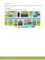
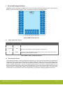
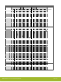
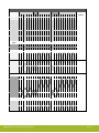
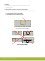
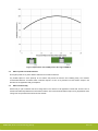
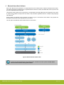
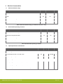
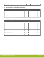
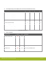
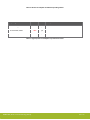
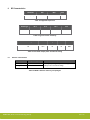
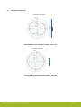
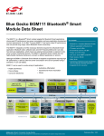
Blue Gecko BGM111 Bluetooth® Smart Module Preliminary Datasheet BGM111 is a Bluetooth Smart module targeted for Bluetooth Smart applications in which good RF performance, low power consumption and easy application development are key requirements. At +8 dBm TX power BGM111 has best-in-class RF performance and can provide long range, robust Bluetooth Smart connectivity. BGM111 integrates all features required for a Bluetooth Smart application: Bluetooth radio, software stack and GATT based profiles and it can also host end user applications, which means no external microcontroller is required in size, price or power constrained devices. BGM111 Bluetooth Smart module also has flexible hardware interfaces to connect to different peripherals or sensors. Although BGM111 Bluetooth Smart Module is targeted for applications requiring high RF performance, it is still has ultra-low power consumption and can be powered using a standard 3 V coin cell battery. KEY FEATURES • • • • • • • • • Bluetooth 4.1 compliant (Bluetooth Smart) Software upgradable to Bluetooth 4.2 TX power: up to +8 dBm RX sensitivity: down to -91 dBm Range: up to 200 meters CPU core: 32-bit ARM® Cortex-M4 Flash memory: 256 kB RAM: 32 kB Autonomous Hardware Crypto Accelerator and True Random Number Generator • Integrated DC-DC Converter silabs.com | Smart. Connected. Energy-friendly This information applies to a product under development. Its characteristics and specifications are subject to change without notice. Silicon Laboratories confidential. Information herein is covered under non-disclosure agreement (NDA) Rev. 0.9 1 Key Features Bluetooth features Bluetooth 4.1 compliant o Software upgradable to Bluetooth 4.2 Hardware interfaces UART host interface 2 x SPI, UART and 2 x I2C peripheral interfaces Central and peripheral roles Up to 25 x GPIO with interrupts Up to 8 x BLE connections in central role 4 x 12-bit ADC and 1 x 12-bit DAC* Internal temperature sensor* Radio features Integrated antenna Internal battery voltage measurement option* TX Power Clock generator* o Real-time counter RX Sensitivity o +8 dBm -91 dBm up to 150 - 200 m LoS range Software features Microcontroller ARM® Cortex-M4F 40 MHz 32 kB RAM Integrated Bluetooth Smart stack 256 kB flash Any GATT based Bluetooth Smart profile Advanced cryptography support 100 kbps throughput over BLE BGAPITM BGLIBTM host API/library which implements BGAPI serial protocol Electrical characteristics Supply voltage: 1.8V to 3.8V with DC/DC bypass mode Supply voltage: 2.4V to 3.8V with DC/DC 8.2 mA TX current at 0 dBm BGScriptTM scripting language for standalone usage 7.5 mA RX current 59 µA/MHz @ Energy Mode 0 Profile ToolkitTM for creating GATT based services 1.7 µA EM2 deep sleep current serial protocol API over UART for modem usage Environmental and regulatory Temperature range: -40°C to +85°C Bluetooth, CE, FCC and IC, Japan and South-Korea qualified* Dimensions: silabs.com | Smart. Connected. Energy-friendly W x L x H: 12.9 mm x 15.0 mm x 2.2 mm Rev. 0.9 1.1 Applications Sports and fitness, health and medical, point-of-sale, consumer electronics, home automation, industrial automation and many more. 1.2 Block diagram The block diagram for the BGM111 Bluetooth Smart module is shown below. Figure 1 BGM111 Block diagram silabs.com | Smart. Connected. Energy-friendly Rev. 0.9 2 Ordering information Part number Description BGM111 Bluetooth Smart Module with internal chip antenna. Cut reel. BGM111A256v1 Features Radio: Bluetooth Smart 4.1, +8 dBm TX Core: ARM Cortex M4 Memory: 32kB RAM / 256kB flash Antenna: chip Packaging: 100 pcs cut reel Status: pre-production samples Production PN: BGM111 Bluetooth Smart Module with internal chip antenna. Full reel. BGM111A256v1 Radio: Bluetooth Smart 4.1, +8 dBm TX Core: ARM Cortex M4 Memory: 32kB RAM / 256kB flash Antenna: chip Packaging: 1000 pcs tape and reel Status: pre-production samples Production PN: Blue Gecko Bluetooth Smart module development kit BGM111A256v2 BGM111A256v2R BGM111 radio board WSTK main board SLWSTK6101A Expansion board (buttons, leds, accelerometer, joystick) Accessories silabs.com | Smart. Connected. Energy-friendly Rev. 0.9 3 Pin-out and Package Definitions This section contains a description of the BGM111 pin-out shown in Figure 2 below. Each pin may have one or more functions. Power, ground and reset pins are listed in Table 1 while GPIO pin assignments are listed in Table 2. Figure 2 BGM111 Pinout (top view) 2.1 Power, ground and reset pins Pad number Function Description 29 VDD Module power supply, supply range 2.4 - 3.8V 1, 12, 20, 31 GND Ground, connected together internally but should all be connected directly to a solid ground plane with vias in close proximity to the pads, especially on the antenna end. 30 RESET Module reset signal. Pulling RESET low will reset the internal processor. This pin has an internal pull-up and can be left floating if not needed. Table 1 BGM111 power, ground and reset pins 2.2 General Purpose I/O pins The 25 GPIO pins of BGM111 module are organized into ports with up to 16 pins each. These GPIO pins can individually be configured as either an output or input. More advanced configurations like open-drain, open-source and glitch filtering can be configured for each individual GPIO pin. GPIO pins can also be overridden by peripheral pin connections like TIMER PWM outputs or USART communication, which can be routed to several locations on the device. The GPIO supports up to 16 asynchronous external pin interrupts, which enable interrupts from any pin on the device. Also, the input value of a pin can be routed through the Peripheral Reflex System to other peripherals. Except for a few special functions, the internal signal crossbar allows various peripheral functions to be assigned freely to any GPIO pad, simplifying application board layout. silabs.com | Smart. Connected. Energy-friendly Rev. 0.9 GPIO ASSIGNMENTS PORT NAME PA PB PC PD PF PORT PIN 0 1 2 3 4 5 11 13 6 7 8 9 10 11 13 14 15 0 1 2 3 4 5 6 7 PAD NUMBER 5 6 7 8 9 10 11 13 14 15 16 17 18 19 2 3 4 21 22 23 24 25 26 27 28 COMMENTS BOOTLOADER • BOOT_RX • BOOT_TX DEBUG • DBG_SWCLKTCK • DBG_SWDIOTMS • DBG_SWO • • • • DBG_TDI • DBG_TDO WAKE UP • GPIO_EM4WU0 • GPIO_EM4WU1 • GPIO_EM4WU4 • GPIO_EM4WU8 • GPIO_EM4WU9 • GPIO_EM4WU12 I2C I2CO_SCL • • • • • • • • • • • • • • • • • • • • • • • • • I2CO_SDA • • • • • • • • • • • • • • • • • • • • • • • • • USART 0 UART SPI US0_CTS US0_CLK • • • • • • • • • • • • • • • • • • • • • • • • • CTS CLK US0_RTS US0_CS • • • • • • • • • • • • • • • • • • • • • • • • • RTS CS US0_RX MISO • • • • • • • • • • • • • • • • • • • • • • • • • RX MISO US0_TX MOSI • • • • • • • • • • • • • • • • • • • • • • • • • TX MOSI UART SPI USART1 US1_CTS US1_CLK • • • • • • • • • • • • • • • • • • • • • • • • • CTS CLK US1_RTS US1_CS • • • • • • • • • • • • • • • • • • • • • • • • • RTS CS US1_RX MISO • • • • • • • • • • • • • • • • • • • • • • • • • RX MISO US1_TX MOSI • • • • • • • • • • • • • • • • • • • • • • • • • TX MOSI LEU0_RX • • • • • • • • • • • • • • • • • • • • • • • • • LEU0_TX • • • • • • • • • • • • • • • • • • • • • • • • • TIM0_CC0 • • • • • • • • • • • • • • • • • • • • • • • • • TIM0_CC1 • • • • • • • • • • • • • • • • • • • • • • • • • LEUART 0 TIMER silabs.com | Smart. Connected. Energy-friendly Rev. 0.9 GPIO ASSIGNMENTS PORT NAME PA PB PC PD PF PORT PIN 0 1 2 3 4 5 11 13 6 7 8 9 10 11 13 14 15 0 1 2 3 4 5 6 7 PAD NUMBER 5 6 7 8 9 10 11 13 14 15 16 17 18 19 2 3 4 21 22 23 24 25 26 27 28 TIM0_CC2 • • • • • • • • • • • • • • • • • • • • • • • • • TIM0_CDTI0 • • • • • • • • • • • • • • • • • • • • • • • • • TIM0_CDTI1 • • • • • • • • • • • • • • • • • • • • • • • • • TIM0_CDTI2 • • • • • • • • • • • • • • • • • • • • • • • • • TIM1_CC0 • • • • • • • • • • • • • • • • • • • • • • • • • TIM1_CC1 • • • • • • • • • • • • • • • • • • • • • • • • • TIM1_CC2 • • • • • • • • • • • • • • • • • • • • • • • • • TIM1_CC3 • • • • • • • • • • • • • • • • • • • • • • • • • LETIM0_OUT0 • • • • • • • • • • • • • • • • • • • • • • • • • LETIM0_OUT1 • • • • • • • • • • • • • • • • • • • • • • • • • COMMENTS LOW ENERGY TIMER ACMP0 • 1X • • • • • • 1Y • • • • • • • 2X • • • • • • • • 2Y 3X • • • • • • • • • • • • 4X • • • • • • • • • • • • • • • • • 3Y 4Y • • • ACMP1 • 1X • • 1Y • • • • • • • 2X • • • • • • • • 2Y 3X • • • • • • • • • • • • 4X • • • • • • • • • • • • • • • • • 3Y 4Y • • • ADC0 1X • • • 1Y • • • • • • • 2X • • • • • • • 2Y silabs.com | Smart. Connected. Energy-friendly • • • • • • • Rev. 0.9 GPIO ASSIGNMENTS PORT NAME PA PB PC PD PF PORT PIN 0 1 2 3 4 5 11 13 6 7 8 9 10 11 13 14 15 0 1 2 3 4 5 6 7 PAD NUMBER 5 6 7 8 9 10 11 13 14 15 16 17 18 19 2 3 4 21 22 23 24 25 26 27 28 3X • • • • 3Y • • • • • • • 4X • • • • • • • 4Y COMMENTS • • • • • • • • IDAC0 1X • 1Y • • • • • • PULSE COUNTER PCNT0_S0IN • • • • • • • • • • • • • • • • • • • • • • • • • PCNT0_S1IN • • • • • • • • • • • • • • • • • • • • • • • • • CLOCK MANAGEMENT • CMU_CLK0 CMU_CLK1 • • • • • • • • • • • Table 2 BGM111 GPIO assignments related to functionalities and peripherals silabs.com | Smart. Connected. Energy-friendly Rev. 0.9 2.3 USART The Universal Synchronous/Asynchronous Receiver/Transmitter is a flexible serial I/O module. It supports full duplex asynchronous UART communication with hardware flow control as well SPI. If UART is used as BGAPI serial protocol host interface it is strongly recommended to use RTS and CTS signals for reliable data transmission. Figure 3 USART 2.4 Low Energy Universal Asynchronous Receiver/Transmitter (LEUART) The unique LEUARTTM provides two-way UART communication on a strict power budget. Only a 32.768 kHz clock is needed to allow UART communication up to 9600 baud. The LEUART includes all necessary hardware to make asynchronous serial communication possible with a minimum of software intervention and energy consumption. 2.5 I2C The I2C module provides an interface between the MCU and a serial I2C bus. It is capable of acting as both a master and a slave. Standard-mode, fast-mode and fast-mode plus speeds are supported, allowing transmission rates from 10 kbit/s up to 1 Mbit/s. Figure 4 I2C silabs.com | Smart. Connected. Energy-friendly Rev. 0.9 2.6 Timer/Counter (TIMER) TIMER peripherals count events, generate PWM outputs. The core of each TIMER is a 16-bit counter. 2.7 Real Time Counter The Real Time Counter is a 32-bit counter providing timekeeping in all energy modes and it is capable of providing system wake-up at user defined instances. The RTCC includes 128 bytes of general purpose data retention, allowing easy and convenient data storage in all energy modes. 2.8 Low Energy Timer (LETIMER) The unique LETIMERTM, is a 16-bit timer that is available in energy mode EM2 DeepSleep in addition to EM1 Sleep and EM0 Active. This allows it to be used for timing and output generation when most of the device is powered down, allowing simple tasks to be performed while the power consumption of the system is kept at an absolute minimum. The LETIMER can be used to output a variety of waveforms with minimal software intervention. 2.9 Ultra Low Power Wake-up Timer (CRYOTIMER) The CRYOTIMER is a 32-bit counter that is capable of running in all energy modes. It can be clocked by either the 32.768 kHz crystal oscillator (LFXO), the 32.768 kHz RC oscillator (LFRCO) or the 1 kHz RC oscillator (ULFRCO). It can provide periodic Wakeup events and PRS signals which can be used to wake up peripherals from any energy mode. The CRYOTIMER provides a wide range of interrupt periods, facilitating flexible ultra-low energy operation. 2.10 Pulse Counter (PCNT) The Pulse Counter (PCNT) peripheral can be used for counting pulses on a single input or to decode quadrature encoded inputs. 2.11 General Purpose Input/Output (GPIO) BGM111 has 25 General Purpose Input/Output pins. Each GPIO pin can be individually configured as either an output or input. More advanced configurations including open-drain, open-source, and glitch-filtering can be configured for each individual GPIO pin. The GPIO pins can be overridden by peripheral connections, like SPI communication. Each peripheral connection can be routed to several GPIO pins on the device. The GPIO subsystem supports asynchronous external pin interrupts. When configured as GPIO output drive strength can be applied to pins on port by port basis and it can be either 1 mA or 10 mA. 2.12 Analog Comparator (ACMP) The Analog Comparator is used to compare the voltage of two analog inputs, with a digital output indicating which input voltage is higher. Inputs are selected from among internal references and external pins. The tradeoff between response time and current consumption is configurable by software. The ACMP can also be used to monitor the supply voltage from software. An interrupt can be generated when the supply falls below or rises above a programmable threshold. 2.13 Analog to Digital Converter (ADC) The ADC is a Successive Approximation Register (SAR) architecture, with a resolution of up to 12 bits up to 1 Msamples/sec. The output sample resolution is configurable and additional resolution is possible using integrated hardware for averaging over multiple samples. The ADC includes integrated voltage references and an integrated temperature sensor. Inputs are selectable from a wide range of source, including pins configurable as either single-ended or differential. silabs.com | Smart. Connected. Energy-friendly Rev. 0.9 2.14 Digital to Analog Current Converter (IDAC) The Digital to Analog Current Converter can source or sink a configurable constant current. This current can be driven on an output pin or routed to the selected ADC input pin for capacitive sensing. The current is programmable between 0.05 μA and 64 μA with several ranges with various step sizes. 2.15 Integrated DC-DC Converter (DC-DC) The DC-DC buck converter covers a wide range of load currents and provides high efficiency in energy modes EM0, EM1, EM2 and EM3. The converter operates in active and bypass operating modes. Bypass mode may be entered when the input voltage is too low for efficient operation of the DC-DC converter. In Bypass mode, the DC-DC input supply is internally connected directly to its output through a low resistance switch. Bypass mode also supports in-rush current limiting to avoid dipping the input supply due to excessive current transients. When DC/DC is enabled, supply voltage range is 2.4 V to 3.6 V. When DC/DC is disabled, supply voltage range is 1.8 V to 3.6 V. When DC/DC is disabled the RX sensitivity improves by 1 dB. silabs.com | Smart. Connected. Energy-friendly Rev. 0.9 4 Antenna This section contain design guidelines and recommendations for the BGM111 antenna. 3.1 PCB design guidelines For optimal performance of the BGM111, please follow the following guidelines: 1. Place the module at the edge of the PCB as shown in the Error! Reference source not found.. 2. Do not place any metal (traces, components, battery etc.) within the clearance area of the antenna. 3. Connect all the GND pins directly to a solid GND plane. 4. Place the GND vias as close to the GND pins as possible. 5. Do not place plastic or any other dielectric material in touch with the antenna. Board edge Min 17mm Min 17mm Metal clearance area Figure 5 Recommended layout for BGM111 Figure 6 Poor layouts for BGM111 silabs.com | Smart. Connected. Energy-friendly Rev. 0.9 Figure 7 Impact of the size of GND plane to the range of BGM111 3.2 Effect of plastic and metal materials Do not place plastic or any other dielectric material in touch with the antenna. Any metallic objects in close proximity to the antenna will prevent the antenna from radiating freely. The minimum recommended distance of metallic and/or conductive objects is 10 mm in any direction from the antenna except in the directions of the application PCB ground planes. 3.3 Effect of human body Human body is quite conductive and has a strong effect on the antenna. If the application is hand held, at least 3 mm of clearance should be kept between the hand and the antenna. This can be achieved with the help of an air gap inside the outer casing of the end product and the antenna of the module. silabs.com | Smart. Connected. Energy-friendly Rev. 0.9 5 Hardware design guidelines BMG111 is an easy-to-apply module with regard to hardware application design but certain design guidelines must be followed to guarantee optimal performance. If these guidelines are not adhered to operation to stated characteristic values cannot be guaranteed. These guidelines are listed in the next sub-sections. 4.1 Power supply requirements Coin cell batteries cannot withstand high peak currents (e.g.. higher than 15 mA). If the peak current exceeds 15 mA it’s recommended to place 47 - 100 µF capacitor in parallel with the coin cell battery to improve the battery life time. Notice that the total current consumption of your application is a combination of the radio, peripherals and MCU current consumption so you must take all of these into account. BGM111 is powered by a unipolar supply voltage with nominal value of 3.3 V. Operating voltage range of the module is 2.4 - 3.8 V when using the built-in DC/DC converter. External high frequency bypass capacitors are not needed because the module contains the required supply filter capacitors. However, care should be taken to prevent strong switching noise from being superimposed on the supply line. Such noise can be generated e.g. by on-board charge pump converters used in RS232 level shifters. Charge pump converters typically have strong switching spikes that are difficult to filter out and such spikes may degrade RF performance. Note that there is a total of about 4.8 µF of ceramic capacitors on the VDD line inside the module. When using low-dropout linear regulators to generate a regulated supply for the VDD line, the stability of the regulator with the low ESR provided by these capacitors should be checked. Many linear regulators and also some switched mode regulators are not stable when using ceramic output capacitors. The datasheet of the regulator typically lists recommendations concerning suitable capacitors including data on ESR range and/or stability curves. A regulator which is stated “stable with ceramic capacitors” is recommended. 4.2 Power saving functions EM power saving modes are automatically controlled by the firmware and it always enters the lowest possible power save mode possible depending on the radio, peripheral and software activity. 4.3 Reset functions BGM111 can be reset by three different methods: by pulling the RESET line low, by the internal watchdog timer or software command. Reset state in BGM111 does not provide power saving functionality and thus cannot be used to save power. BGM111 has an internal system power-up reset function. The RESET pin includes an on-chip pull-up resistor and can therefore be left unconnected if no external reset switch or source is needed. 4.4 4.4.1 Debug and firmware updates JTAG It is recommended to expose the JTAG debug pins in your own hardware design for firmware update and debug purposes. The following table lists the required pins for JTAG connection. The debug pins have pull-down and pull-up enabled by default, so leaving them enabled may increase current consumption if left connected to supply or ground. If enabling the JTAG pins the module must be power cycled to enable a SWD debug session. PAD NAME PAD NUMBER JTAG SIGNAL NAME COMMENTS PF3 24 TDI This pin is disabled after reset. Once enabled the pin has a built-in pull-up. PF2 23 TDO This pin is disabled after reset silabs.com | Smart. Connected. Energy-friendly Rev. 0.9 PF1 22 TMS Pin is enabled after reset and has a built-in pull-up PF0 21 TCK Pin is enabled after reset and has a built-in pull-down Table 3 JTAG pads in BGM111 4.4.2 DFU It is also possible to update the firmware over UART using DFU protocol. However the bootloader cannot be updated using DFU but requires that the firmware is updated using JTAG. silabs.com | Smart. Connected. Energy-friendly Rev. 0.9 6 Bluetooth Smart Stack Software Silicon Labs’ Bluetooth Smart Software is a complete Bluetooth Smart software stack for BGM111 Bluetooth Smart module. The software implements a full Bluetooth LE compatible Bluetooth Stack and L2CAP, RFCOMM, SMP and ATT protocols and any GATT based Bluetooth Smart profile. The Bluetooth Smart Software also is supported by a complete SDK for developing Bluetooth Smart applications using either an external host or BGAPITM serial protocol over UART or fully standalone applications based on a simple scripting language called BGScriptTM. Several profiles and software project examples are offered as part of the Bluetooth Smart SDK to help expedite the development of Bluetooth Smart compatible end-user products. The main parts of the Bluetooth Smart software stack are shown below. Figure 8 Bluetooth Smart software stack To learn more about the Bluetooth Smart software stack, the SDK and the APIs please read Blue Gecko Bluetooth Smart Software Getting Started Guide. silabs.com | Smart. Connected. Energy-friendly Rev. 0.9 7 Host interface 6.1 UART BGM111 can be controlled over the UART interface. In order for the communication to be reliable for any amounts of data exceeding short, intermittent commands, hardware flow control signals (RTS and CTS) must be present between the host and the module. The controlling processor should have a clock frequency accurate to within 1% in order for the UART signaling to work reliably with speeds exceeding 115.200 kbps. silabs.com | Smart. Connected. Energy-friendly Rev. 0.9 8 Electrical characteristics 7.1 Absolute maximum ratings Rating Min Max Unit Storage Temperature -50 150 °C VDD -0.3 3.8 V 5V tolerant GPIO Voltages -0.3 5.25* V Other Terminal Voltages -0.3 VDD+0.3 V Table 4 Absolute maximum ratings (*or VDD+2V, whichever is less) 7.2 Recommended operating conditions Rating Min Max Unit Operating Temperature Range -40 85 °C VDD when using internal DC/DC 2.4 3.8 V VDD when DC/DC in bypass mode 1.8 3.8 V VDD (when operating ADC or DAC) 1.8 3.8 V Table 5 Recommended operating conditions 7.3 Input/output terminal characteristics Digital terminals Min Typ Max Unit Input voltage levels VIL input logic level low 1.7V ≤ VDD ≤ 3.6V -0.3 0.3VDD V VIH input logic level high 1.7V ≤ VDD ≤ 3.6V 0.7VDD VDD+2.0 V 0.2*VDD V Output voltage levels VOL output logic level low, Vdd = 3.3 V, Iol = 3 mA, weak driver VOH output logic level high Vdd = 3.3 V, Ioh = -3 mA, weak driver VOL output logic level low, Vdd = 3.3 V, Iol = 20 mA, strong driver silabs.com | Smart. Connected. Energy-friendly 0.8*VDD V 0.2*VDD V Rev. 0.9 VOH output logic level high Vdd = 3.3 V, Ioh = -20 mA, strong driver 0.8*VDD V Table 6 Digital terminal electrical characteristics 7.4 Reset signal (need to be checked from SOC data sheet values) Power-on Reset Min Typ Max Unit Power on reset threshold (rising edge) 1.84 1.92 2.00 V Power on reset threshold (falling edge) 1.80 1.88 1.96 V RESET signal pulse width (pulled low) 500 ns Table 7 Reset characteristics 7.5 Analog Digital Converter (ADC) (need to be checked from SOC data sheet values) Power-on Reset Min ADC input impedance Typ Max 670 Unit kohm ADC input voltage range 0 2*Vref V Resolution (programmable) 6 12 bits 1 MSps Sampling rate Offset error 1 LSB Differential non-linearity -1 1 LSB Integral non-linearity -3 3 LSB Table 8 ADC characteristics silabs.com | Smart. Connected. Energy-friendly Rev. 0.9 7.6 Current Digital Analog Converter (IDAC) (need to be checked from SOC data sheet values) Power-on Reset Min Steps per range Typ Max Unit 31 DAC output current range (range 0) 0.05 1.6 µA DAC output current range (range 1) 1.6 4.6 µA DAC output current range (range 2) 0.5 16 µA DAC output current range (range 3) 2 64 µA Total error (continuous mode) -1 1 % Total error (duty cycle mode) -2 2 % Settling time to 1% (range changed) 5 µs Settling time to 1% (step changed) 1 µs Table 9 IDAC characteristics 7.7 Power consumption Operation state Current Unit Transmit, +8dBm, 1Mbps TBD mA Transmit, 0dBm 8.2 mA Receive 7.5 mA Radio off, CPU active TBD µA/MHz Radio off, CPU idle TBD µA/MHz Deep sleep mode TBD µA RTC running, full RAM retention Shutdown mode TBD µA RTC running, 128B RAM retention Full shutdown mode TBD µA No RTC, no RAM retention silabs.com | Smart. Connected. Energy-friendly Description Rev. 0.9 Table 10 Power consumption for different operating modes Operating mode Current Unit LE advertising, discoverable TBD µA LE connected, master TBD µA LE connected, slave TBD µA Description Table 11 Typical power consumption in practical use cases silabs.com | Smart. Connected. Energy-friendly Rev. 0.9 9 RF Characteristics Parameter Min Max Unit Frequency 2402 2480 MHz Table 12 Supported frequencies Packet type -40oC 20oC 85oC Unit LE TBD -91 TBD dBm Table 13 Typical receiver sensitivity Modulation type Min Typ Max Unit LE +6.5 +8 +9 dBm Table 14 Transmitter output power at maximum setting 8.1 Antenna characteristics Parameter With optimal layout Note Efficiency -2 dB Peak gain +1 dBi Efficiency and peak gain depend on the application PCB layout and mechanical design Table 15 BGM111 Antenna efficiency and peak gain silabs.com | Smart. Connected. Energy-friendly Rev. 0.9 8.2 2D Radiation Pattern Plots 2D pattern, front view 5 dB 0 dB -5 dB -10 dB -15 dB -20 dB 50 mm -25 dB Figure 9 BGM111 typical 2D radiation pattern – front view 2D pattern, side view 5 dB 0 dB -5 dB -10 dB -15 dB -20 dB -25 dB Figure 10 BGM111 typical 2D radiation pattern – side view silabs.com | Smart. Connected. Energy-friendly Rev. 0.9 2D pattern, top view 5 dB 0 dB -5 dB -10 dB -15 dB -20 dB -25 dB 16 mm 50 mm Figure 11 BGM111 typical 2D radiation pattern – top view silabs.com | Smart. Connected. Energy-friendly Rev. 0.9 8.3 Physical dimensions Figure 12 Module physical dimensions silabs.com | Smart. Connected. Energy-friendly Rev. 0.9 Figure 13 Recommended PCB land pattern 2.0 mm 0.72 mm Figure 14 BGM111 sideways dimensions silabs.com | Smart. Connected. Energy-friendly Rev. 0.9 10 Soldering recommendations BGM111 is compatible with industrial standard reflow profile for Pb-free solders. The reflow profile used is dependent on the thermal mass of the entire populated PCB, heat transfer efficiency of the oven and particular type of solder paste used. Consult the datasheet of particular solder paste for profile configurations. We will give following recommendations for soldering the module to ensure reliable solder joint and operation of the module after soldering. Since the profile used is process and layout dependent, the optimum profile should be studied case by case. Thus following recommendation should be taken as a starting point guide. Refer to technical documentations of particular solder paste for profile configurations Avoid using more than one flow. Reliability of the solder joint and self-alignment of the component are dependent on the solder volume. Minimum of 150 m stencil thickness is recommended. Aperture size of the stencil should be 1:1 with the pad size. A low residue, “no clean” solder paste should be used due to low mounted height of the component. If the vias used on the application board have a diameter larger than 0.3 mm, it is recommended to mask the via holes at the module side to prevent solder wicking through the via holes. Solders have a habit of filling holes and leaving voids in the thermal pad solder junction, as well as forming solder balls on the other side of the application board which can in some cases be problematic. silabs.com | Smart. Connected. Energy-friendly Rev. 0.9 11 Certifications The certifications for the BGM111 Bluetooth Smart module are pending. 10.1 Bluetooth Bluetooth qualifications are pending. 10.2 CE BGM111 is in conformity with the essential requirements and other relevant requirements of the R&TTE Directive (1999/5/EC). This device is compliant with the following standards: Safety: EN 60950 EMC: EN 301 489 Spectrum: EN 300 328 RF Exposure: EN 62479 Formal DoC is available from www.silabs.com. 10.3 FCC This device complies with Part 15 of the FCC Rules. Operation is subject to the following two conditions: (1) this device may not cause harmful interference, and (2) this device must accept any interference received, including interference that may cause undesired operation. Any changes or modifications not expressly approved by Bluegiga Technologies could void the user’s authority to operate the equipment. FCC RF Radiation Exposure Statement: This equipment complies with FCC radiation exposure limits set forth for an uncontrolled environment. End users must follow the specific operating instructions for satisfying RF exposure compliance. This transmitter meets both portable and mobile limits as demonstrated in the RF Exposure Analysis. This transmitter must not be co-located or operating in conjunction with any other antenna or transmitter except in accordance with FCC multi-transmitter product procedures. As long as the condition above is met, further transmitter testing will not be required. However, the OEM integrator is still responsible for testing their end-product for any additional compliance requirements required with this module installed (for example, digital device emissions, PC peripheral requirements, etc.). OEM Responsibilities to comply with FCC Regulations The BGM111 Module has been certified for integration into products only by OEM integrators under the following condition: The transmitter module must not be co-located or operating in conjunction with any other antenna or transmitter except in accordance with FCC multi-transmitter product procedures. As long as the condition above is met, further transmitter testing will not be required. However, the OEM integrator is still responsible for testing their end-product for any additional compliance requirements required with this module installed (for example, digital device emissions, PC peripheral requirements, etc.). silabs.com | Smart. Connected. Energy-friendly Rev. 0.9 IMPORTANT NOTE: In the event that this condition cannot be met (for certain configurations or co-location with another transmitter), then the FCC authorization is no longer considered valid and the FCC ID cannot be used on the final product. In these circumstances, the OEM integrator will be responsible for re-evaluating the end product (including the transmitter) and obtaining a separate FCC authorization. End Product Labeling The BGM111 module is labeled with its own FCC ID. If the FCC ID is not visible when the module is installed inside another device, then the outside of the device into which the module is installed must also display a label referring to the enclosed module. In that case, the final end product must be labeled in a visible area with the following: “Contains Transmitter Module FCC ID: TBD” or “Contains FCC ID: TBD The OEM integrator has to be aware not to provide information to the end user regarding how to install or remove this RF module or change RF related parameters in the user manual of the end product. 10.4 IC This radio transmitter has been approved by Industry Canada to operate with the embedded chip antenna. Other antenna types are strictly prohibited for use with this device. This device complies with Industry Canada’s license-exempt RSS standards. Operation is subject to the following two conditions: (1) This device may not cause interference; and (2) This device must accept any interference, including interference that may cause undesired operation of the device RF Exposure Statement Exception from routine SAR evaluation limits are given in RSS-102 Issue5. BGM111 meets the given requirements when the minimum separation distance to human body is less than equal to 15 mm. RF exposure or SAR evaluation is not required when the separation distance is 15 mm or more. If the separation distance is less than 15 mm the OEM integrator is responsible for evaluating the SAR. OEM Responsibilities to comply with IC Regulations The BGM111 Module has been certified for integration into products only by OEM integrators under the following conditions: The antenna(s) must be installed such that a minimum separation distance of 15 mm is maintained between the radiator (antenna) and all persons at all times. The transmitter module must not be co-located or operating in conjunction with any other antenna or transmitter. As long as the two conditions above are met, further transmitter testing will not be required. However, the OEM integrator is still responsible for testing their end-product for any additional compliance requirements required with this module installed (for example, digital device emissions, PC peripheral requirements, etc.). IMPORTANT NOTE: In the event that these conditions cannot be met (for certain configurations or co-location with another transmitter), then the IC authorization is no longer considered valid and the IC ID cannot be used on the final product. In silabs.com | Smart. Connected. Energy-friendly Rev. 0.9 these circumstances, the OEM integrator will be responsible for re-evaluating the end product (including the transmitter) and obtaining a separate IC authorization End Product Labeling The BGM111 module is labeled with its own IC ID. If the IC ID is not visible when the module is installed inside another device, then the outside of the device into which the module is installed must also display a label referring to the enclosed module. In that case, the final end product must be labeled in a visible area with the following: “Contains Transmitter Module IC: TBD” or “Contains IC: TBD The OEM integrator has to be aware not to provide information to the end user regarding how to install or remove this RF module or change RF related parameters in the user manual of the end product 10.4.1 IC Cet émetteur radio (IC : TBD) a reçu l'approbation d'Industrie Canada pour une exploitation avec l'antenne puce incorporée. Il est strictement interdit d'utiliser d'autres types d'antenne avec cet appareil. Le présent appareil est conforme aux CNR d’Industrie Canada applicables aux appareils radio exempts de licence. L’exploitation est autorisée aux deux conditions suivantes : 1) l’appareil ne doit pas produire de brouillage; 2) l’utilisateur de l’appareil doit accepter tout brouillage radioélectrique subi, même si le brouillage est susceptible d’en compromettre le fonctionnement. Déclaration relative à l'exposition aux radiofréquences (RF) Les limites applicables à l’exemption de l’évaluation courante du DAS sont énoncées dans le CNR 102, 5e édition. L'appareil BGM111 répond aux exigences données quand la distance de séparation minimum par rapport au corps humain est inférieure ou égale à 15 mm. L'évaluation de l'exposition aux RF ou du DAS n'est pas requise quand la distance de séparation est de 15 mm ou plus. Si la distance de séparation est inférieure à 15 mm, il incombe à l'intégrateur FEO d'évaluer le DAS. Responsabilités du FEO ayant trait à la conformité avec les règlements IC Le module BGM111 a été certifié pour une intégration dans des produits uniquement par les intégrateurs FEO dans les conditions suivantes : La ou les antennes doivent être installées de telle façon qu'une distance de séparation minimum de 15 mm soit maintenue entre le radiateur (antenne) et toute personne à tout moment. Le module émetteur ne doit pas être installé au même endroit ou fonctionner conjointement avec toute autre antenne ou émetteur. Dès lors que les deux conditions ci-dessus sont respectées, d'autres tests de l'émetteur ne sont pas obligatoires. Cependant, il incombe toujours à l'intégrateur FEO de tester la conformité de son produit final vis-à-vis de toute exigence supplémentaire avec ce module installé (par exemple, émissions de dispositifs numériques, exigences relatives aux matériels périphériques PC, etc). silabs.com | Smart. Connected. Energy-friendly Rev. 0.9 REMARQUE IMPORTANTE : S'il s'avère que ces conditions ne peuvent être respectées (pour certaines configurations ou la colocation avec un autre émetteur), alors l'autorisation IC n'est plus considérée comme valide et l'identifiant IC ne peut plus être employé sur le produit final. Dans ces circonstances, l'intégrateur FEO aura la responsabilité de réévaluer le produit final (y compris l'émetteur) et d'obtenir une autorisation IC distincte. Étiquetage du produit final L'étiquette du module BGM111 porte son propre identifiant IC. Si l'identifiant IC n'est pas visible quand le module est installé à l'intérieur d'un autre appareil, l'extérieur de l'appareil dans lequel le module est installé doit aussi porter une étiquette faisant référence au module qu'il contient. Dans ce cas, une étiquette comportant les informations suivantes doit être collée sur une partie visible du produit final : « Contient le module émetteur IC : TBD » ou « Contient IC : TBD » L'intégrateur FEO doit être conscient de ne pas fournir d'informations à l'utilisateur final permettant d'installer ou de retirer ce module RF ou de changer les paramètres liés aux RF dans le mode d'emploi du produit final. silabs.com | Smart. Connected. Energy-friendly Rev. 0.9 12 Revision history 11.1 Revision 0.9 Preliminary silabs.com | Smart. Connected. Energy-friendly Rev. 0.9 1 Key Features ....................................................................................................................................................................... 2 1.1 Applications .................................................................................................................................................................. 3 1.2 Block diagram............................................................................................................................................................... 3 2 Ordering information ......................................................................................................................................................... 4 3 Pin-out and Package Definitions....................................................................................................................................... 5 4 5 2.1 Power, ground and reset pins....................................................................................................................................... 5 2.2 General Purpose I/O pins ............................................................................................................................................. 5 2.3 USART ......................................................................................................................................................................... 9 2.4 Low Energy Universal Asynchronous Receiver/Transmitter (LEUART) ....................................................................... 9 2.5 I2C ................................................................................................................................................................................ 9 2.6 Timer/Counter (TIMER) .............................................................................................................................................. 10 2.7 Real Time Counter ..................................................................................................................................................... 10 2.8 Low Energy Timer (LETIMER) ................................................................................................................................... 10 2.9 Ultra Low Power Wake-up Timer (CRYOTIMER) ....................................................................................................... 10 2.10 Pulse Counter (PCNT) ............................................................................................................................................... 10 2.11 General Purpose Input/Output (GPIO) ....................................................................................................................... 10 2.12 Analog Comparator (ACMP)....................................................................................................................................... 10 2.13 Analog to Digital Converter (ADC) .............................................................................................................................. 10 2.14 Digital to Analog Current Converter (IDAC) ................................................................................................................ 11 2.15 Integrated DC-DC Converter (DC-DC) ....................................................................................................................... 11 Antenna ............................................................................................................................................................................. 12 3.1 PCB design guidelines ............................................................................................................................................... 12 3.2 Effect of plastic and metal materials ........................................................................................................................... 13 3.3 Effect of human body ................................................................................................................................................. 13 Hardware design guidelines ............................................................................................................................................ 14 4.1 Power supply requirements ........................................................................................................................................ 14 4.2 Power saving functions .............................................................................................................................................. 14 4.3 Reset functions........................................................................................................................................................... 14 4.4 Debug and firmware updates ..................................................................................................................................... 14 6 Bluetooth Smart Stack Software ..................................................................................................................................... 16 7 Host interface ................................................................................................................................................................... 17 6.1 8 UART ......................................................................................................................................................................... 17 Electrical characteristics ................................................................................................................................................. 18 7.1 Absolute maximum ratings ......................................................................................................................................... 18 7.2 Recommended operating conditions .......................................................................................................................... 18 7.3 Input/output terminal characteristics ........................................................................................................................... 18 7.4 Reset signal (need to be checked from SOC data sheet values) ............................................................................... 19 7.5 Analog Digital Converter (ADC) (need to be checked from SOC data sheet values) ................................................. 19 silabs.com | Smart. Connected. Energy-friendly Rev. 0.9 7.6 Current Digital Analog Converter (IDAC) (need to be checked from SOC data sheet values) ................................... 20 7.7 Power consumption .................................................................................................................................................... 20 9 RF Characteristics............................................................................................................................................................ 22 8.1 Antenna characteristics .............................................................................................................................................. 22 8.2 2D Radiation Pattern Plots ......................................................................................................................................... 23 8.3 Physical dimensions ................................................................................................................................................... 25 10 Soldering recommendations ....................................................................................................................................... 27 11 Certifications ................................................................................................................................................................ 28 10.1 Bluetooth .................................................................................................................................................................... 28 10.2 CE .............................................................................................................................................................................. 28 10.3 FCC ............................................................................................................................................................................ 28 10.4 IC ................................................................................................................................................................................ 29 12 11.1 Revision history ........................................................................................................................................................... 32 Revision 0.9................................................................................................................................................................ 32 silabs.com | Smart. Connected. Energy-friendly Rev. 0.9