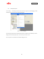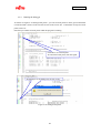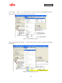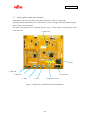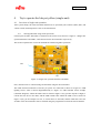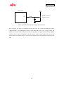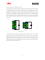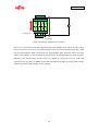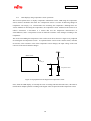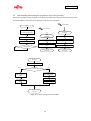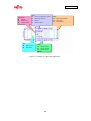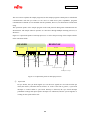
1
AN07-00200-03E F2MC-8FX Family 8-BIT MICROCONTROLLER MB95F136JBS bits pot yellow LIN board User’s Manual AN07-00200-03E Revision History Date Revision October.24.2008 Revision 1.0: Initial release May 13, 2009 Revision 1.1:TSUZUKI DENSAN’s Logo mark was changed. April 23,2010 Revision 1.2: Change in company name of FUJITSU MICROELECTORONICS [New] FUJITSU SEMICONDUCTOR LIMITED (left blank) 2 AN07-00200-03E Note - The contents of this document are subject to change without notice. Customers are advised to consult with FUJITSU sales representatives before ordering. - The information, such as descriptions of function and application circuit examples, in this document are presented solely for the purpose of reference to show examples of operations and uses of Fujitsu semiconductor device; Fujitsu does not warrant proper operation of the device with respect to use based on such information. When you develop equipment incorporating the device based on such information, you must assume any responsibility arising out of such use of the information. Fujitsu assumes no liability for any damages whatsoever arising out of the use of the information. - Any information in this document, including descriptions of function and schematic diagrams, shall not be construed as license of the use or exercise of any intellectual property right, such as patent right or copyright, or any other right of Fujitsu or any third party or does Fujitsu warrant non-infringement of any third-party’s intellectual property right or other right by using such information. Fujitsu assumes no liability for any infringement of the intellectual property rights or other rights of third parties which would result from the use of information contained herein. - The products described in this document are designed, developed and manufactured as contemplated for general use, including without limitation, ordinary industrial use, general office use, personal use, and household use, but are not designed, developed and manufactured as contemplated (1) for use accompanying fatal risks or dangers that, unless extremely high safety is secured, could have a serious effect to the public, and could lead directly to death, personal injury, severe physical damage or other loss (i.e., nuclear reaction control in nuclear facility, aircraft flight control, air traffic control, mass transport control, medical life support system, missile launch control in weapon system), or (2) for use requiring extremely high reliability (i.e., submersible repeater and artificial satellite). Please note that Fujitsu will not be liable against you and/or any third party for any claims or damages arising in connection with above-mentioned uses of the products. - Any semiconductor devices have an inherent chance of failure. You must protect against injury, fire, damage or loss from such failures by incorporating safety design measures into your facility and equipment such as redundancy, fire protection, and prevention of over-current levels and other abnormal operating conditions. - If any products described in this document represent goods or technologies subject to certain restrictions on export under the Foreign Exchange and Foreign Trade Law of Japan, the prior authorization by Japanese government will be required for export of those products from Japan. - The company names and brand names herein are the trademarks or registered trademarks of their respective owners. Copyright© 2010 FUJITSU SEMICONDUCTOR LIMITED all rights reserved 3 AN07-00200-03E Table of Contents Revision History ........................................................................................................................2 Note ..........................................................................................................................................3 Introduction ............................................................................................................................ 10 Contact .................................................................................................................................... 11 Suppliers of the parts/materials ................................................................................................. 12 1 Setting up the starter kit .................................................................................................... 13 1.1 Setting up the PC ...................................................................................................... 21 1.1.1 Downloading the software ..................................................................................... 22 1.1.2 Installing the integrated development environment SOFTUNE (bits pot yellow dedicated version) ............................................................................................................ 22 1.1.3 Installing the PC Writer FUJITSU FLASH USB Programmer (bits pot yellow dedicated version) ........................................................................................................................... 27 1.1.4 Connecting it to the PC and installing the USB driver .............................................. 30 1.1.5 Configuring the starter kit ...................................................................................... 33 2 Running the Program ....................................................................................................... 35 2.1 Executing in single chip mode ................................................................................... 36 2.1.1 Building a project ................................................................................................. 36 2.1.2 Writing the program into the microcontroller .......................................................... 40 2.2 Debugging by using Monitor Debugger ...................................................................... 43 2.2.1 Activating SOFTUNE and configuring the debug settings ........................................ 43 2.2.2 Writing the monitor program into the microcontroller .............................................. 53 2.2.3 Loading the target file ........................................................................................... 56 2.2.4 Running the debugger ........................................................................................... 57 3 4 Operation of the sample Programs ..................................................................................... 60 3.1 bits pot yellow single-unit operation........................................................................... 61 3.2 LIN communication operation (LIN communication operation with the bits pot white) .. 63 Try to operate the bits pot yellow (single-unit) ................................................................... 65 4.1 Overview of single-unit operation .............................................................................. 65 4.1.1 Turning ON LEDs using switch operations ............................................................. 65 4.1.2 Controlling the buzzer using the volume switch....................................................... 69 4.1.3 LED displays using temperature sensor operations .................................................. 73 4.2 5 Understanding and running the program in single-unit operation .................................. 74 Try to use LIN communication ......................................................................................... 79 5.1 What is LIN? ............................................................................................................ 79 4 AN07-00200-03E 5.2 LIN specifications .................................................................................................... 82 5.2.1 Lin frame configuration ......................................................................................... 82 5.3 LIN communication flow .......................................................................................... 85 5.4 Communication between master and slave if an error occurs ........................................ 87 5.5 LIN communication by using microcontroller ............................................................. 88 5.6 Understanding and overview of the program for LIN communication ........................... 92 5.6.1 LIN communication configuration.......................................................................... 92 5.6.2 Sample programs sequence .................................................................................... 97 6 Appendix ...................................................................................................................... 109 6.1 Sample program folder/file configuration ................................................................. 109 5 AN07-00200-03E List of Figures Figure 1-1 External view of a starter kit ............................................................................. 14 Figure 1-2 System connection diagram (single-unit operation) ............................................ 17 Figure 1-3 System connection diagram (when performing LIN communication) ................... 18 Figure 1-4 SOFTUNE setup confirmation .......................................................................... 22 Figure 1-5 Starting SOFTUNE setup ................................................................................. 22 Figure 1-6 SOFTUNE setup confirmation .......................................................................... 23 Figure 1-7 SOFTUNE setup/License agreement ................................................................. 23 Figure 1-8 SOFTUNE setup/Version information ............................................................... 24 Figure 1-9 SOFTUNE setup/Selecting the destination of installation .................................... 24 Figure 1-10 SOFTUNE setup/Selecting the components ..................................................... 25 Figure 1-11 SOFTUNE setup/Confirming the installation settings ....................................... 25 Figure 1-12 SOFTUNE setup/Completion ......................................................................... 26 Figure 1-13 PC writer/Installation dialog ........................................................................... 27 Figure 1-14 PC Writer/Setup type...................................................................................... 28 Figure 1-15 Finished PC writer/Ready to install ................................................................. 28 Figure 1-16 Completing the PC Writer installation ............................................................. 29 Figure 1-17 Installing BGM Adapter (MB2146-09) ............................................................ 30 Figure 1-18 Selecting the search locations ......................................................................... 31 Figure 1-19 Hardware installation ..................................................................................... 31 Figure 1-20 Completing the BGM Adapter (MB2146-09) installation .................................. 32 Figure 1-21 MODE selection ............................................................................................ 33 Figure 1-22 Connection between the PC and the starter kit .................................................. 34 Figure 2-1 SOFTUNE Workbench start window ................................................................. 36 Figure 2-2 Opening a workspace ....................................................................................... 37 Figure 2-3 Selecting a workspace ...................................................................................... 37 Figure 2-4 Setting the active project .................................................................................. 38 Figure 2-5 Changing the active project .............................................................................. 38 Figure 2-6 Building a project ............................................................................................ 39 Figure 2-7 Completing the build........................................................................................ 39 Figure 2-8 Opening the file to write ................................................................................... 40 Figure 2-9 Selecting the file to write .................................................................................. 41 Figure 2-10 Writing the program ....................................................................................... 41 Figure 2-11 Completing the program writing...................................................................... 42 Figure 2-12 Opening a workspace ..................................................................................... 43 6 AN07-00200-03E Figure 2-13 Selecting a workspace .................................................................................... 44 Figure 2-14 Building a project .......................................................................................... 45 Figure 2-15 Completing the build ...................................................................................... 45 Figure 2-16 Load module outputs ...................................................................................... 46 Figure 2-17 Debug settings ............................................................................................... 47 Figure 2-18 Changing the debug settings ........................................................................... 47 Figure 2-19 Starting the debug setting wizard..................................................................... 48 Figure 2-20 Selecting the debugger type ............................................................................ 48 Figure 2-21 Entering password when starting debugger ...................................................... 49 Figure 2-22 Selecting the device type ................................................................................ 49 Figure 2-23 Setting the primary oscillation frequency ......................................................... 50 Figure 2-24 Specifying a batch file ................................................................................. 50 Figure 2-25 Configuring the target file settings................................................................... 51 Figure 2-26 Setting setup file selection .............................................................................. 51 Figure 2-27 Completing the setup wizard ........................................................................... 52 Figure 2-28 Completing the project settings ....................................................................... 52 Figure 2-29 Opening the file to write ................................................................................. 53 Figure 2-30 Selecting the file to write ................................................................................ 54 Figure 2-31 Writing the program ....................................................................................... 55 Figure 2-32 Completing the program writing ..................................................................... 55 Figure 2-33 Start debugging.............................................................................................. 56 Figure 2-34 Setting break points........................................................................................ 57 Figure 2-35 Running the program...................................................................................... 58 Figure 2-36 Stopping the program ..................................................................................... 58 Figure 3-1 Single-unit operation/Controls and mechanicals ................................................. 61 Figure 3-2 LIN communication operation/Controls and mechanicals.................................... 63 Figure 4-1 Single-unit operation/Switches and LEDs .......................................................... 65 Figure 4-2 LED lighting circuit ......................................................................................... 66 Figure 4-3 LED ON/OFF circuit example (schematic diagram) ........................................... 66 Figure 4-4 Connection configuration between SW2 and microcontroller pins (schematic diagram) .................................................................................................................. 67 Figure 4-5 Single-unit operation/Volume SW ..................................................................... 69 Figure 4-6 Volume SW (variable resistor) .......................................................................... 69 Figure 4-7 Circuit surrounding the voltage adjustment knob ................................................ 70 Figure 4-8 Piezoelectricity ................................................................................................ 71 Figure 4-9 Principle of piezoelectric elements .................................................................... 72 7 AN07-00200-03E Figure 4-10 peripheral circuit diagram for temperature sensor ............................................. 73 Figure 4-11 Single-unit operation flowcharts ...................................................................... 74 Figure 4-12 Operation mode settings (when using volume switch) ....................................... 75 Figure 4-13 Operation mode settings (when using the temperature sensor) ........................... 75 Figure 4-14 Main function program................................................................................... 76 Figure 4-15 SW2 interrupts (LED on/off processing) .......................................................... 77 Figure 4-16 SW3 interrupts (buzzer output processing) ....................................................... 77 Figure 4-17 A/D converter interrupts ................................................................................. 78 Figure 5-1 Example of vehicle LIN applications ................................................................. 80 Figure 5-2 Main LIN network configuration ...................................................................... 81 Figure 5-3 LIN communication flow ................................................................................. 83 Figure 5-4 LIN frame configuration .................................................................................. 83 Figure 5-5 Main LIN network configuration ...................................................................... 86 Figure 5-6 Example of communication sequence between the master and slaves during normal communication ......................................................................................................... 86 Figure 5-7 LIN circuit ...................................................................................................... 88 Figure 5-8 Entire LIN communication control registers....................................................... 89 Figure 5-9 LIN communication flowchart (main routine) .................................................... 97 Figure 5-10 LIN communication flowchart (interrupt routine: UART reception interrupts) .... 98 Figure 5-11 LIN communication flowchart (interrupt routine: input capture interrupts) ......... 98 Figure 5-12 Operations points of interrupt processes........................................................... 99 Figure 5-13 Synch break interrupt control ........................................................................ 100 Figure 5-14 Input capture operation in the synch field....................................................... 101 Figure 5-15 Input capture (ICU) interrupt controls ............................................................ 102 Figure 5-16 LIN-UART receive interrupt control .............................................................. 103 Figure 5-17 Receive determination processing ................................................................. 104 Figure 5-18 Timeout detection processing ........................................................................ 105 Figure 5-19 Data send processing .................................................................................... 106 Figure 5-20 Data reception processing ............................................................................. 107 Figure 5-21 Submain processing ..................................................................................... 108 8 AN07-00200-03E List of Tables Table 1-1 Component list .................................................................................................. 13 Table 1-2 Description of the respective parts of a starter kit ................................................. 15 Table 1-3 MB95F136JBS pin assignment .......................................................................... 19 Table 3-1 Single-unit operation/Descriptions of the controls and mechanicals ....................... 62 Table 3-2 LIN communication/Descriptions of the controls and mechanicals ........................ 64 Table 5-1 Description of the entire LIN communication control registers and setting values .. 90 Table 5-2 LIN communication conditions of the sample program ........................................ 92 Table 5-3 LIN message IDs in the sample program ............................................................. 92 Table 6-1 Sample program folder/file configuration .......................................................... 109 9 AN07-00200-03E Introduction Thank you very much for purchasing the bits pot yellow (referred to as this starter kit or the starter kit hereafter). This starter kit is a beginner’s kit intended for those who wish to start learning microcontrollers and on-board network processors. The kit is designed so that the beginners who ask “What is a microcontroller?”, “How does it work?” and “How does it control a network?” can easily learn what it is. The kit includes flash microcontroller development tools, so if you have slight understanding about the C language, you can rewrite a program to let the microcontroller perform in various ways. Even if you do not know of programming, you may be able to enjoy learning a microcontroller with a study-aid book about the C language. This starter kit can also serve as an introductory training tool for electronic circuit practice or future embedded software development in a class of a college or high school of technology or training for freshman engineers of a manufacturer. 10 AN07-00200-03E Contact Please ask the following e-mail address for the technical question. Please confirm HP for the latest information and FAQ of bits pot. Zip code: 105-8420 2-5-3 Nishi-Shinbashi, Minatoku, Tokyo E-mail: [email protected] bits pot URL: http://www.tsuzuki-densan.co.jp/bitspot/ 11 AN07-00200-03E Suppliers of the parts/materials Capacitors 22pF : GCM1552C1H220JZ02 220pF : GCM1552C1H221JA01 0.1μF : GCM188R11E104KA42 10μF : GCM32ER71E106KA42 Ceramic Resonator 4MHz : CSTCR4M00G55B 6MHz : CSTCR6M00G55B Buzzer : PKLCS1212E40A1 NTC Thermistor : NTCG164BH103JT1 Ferrite Beads : MPZ2012S300AT 12 AN07-00200-03E 1 Setting up the starter kit Before using this starter kit, be sure to check the components listed in Table 1-1 are fully supplied. Before connecting this starter kit, you need to install software in your PC. You can download the software required for the starter kit from our web site. bits pot URL: http://www.tsuzuki-densan.co.jp/bitspot/ Table 1-1 Component list No. Article Qty. Specifications Remarks 1 bits pot yellow 1 Board mounted with microcontrollers made by See Figure 1-1 LIN board Fujitsu Semiconductor; F2MC-8FX 2 series MB95F136JBS and F MC-8LX series MB89P585B 2 USB cable 1 USB (A to miniB) Accessory 3 LIN cable 1 2-pin cable Accessory 4 PC 1 On which Windows XP normally runs and Prepare the PC by USB2.0 ports are supported yourself. 13 AN07-00200-03E 14. LIN transceiver IC 19. Jumper pin 13. Regulator 12. LIN connector 11. USB connector 22. LIN transceiver IC Extension power (12V) 20. Extension power (5V) 10. Power LED lamp 21. Extension GND 1. Target device 15. Reset IC 16. Oscillator for USB communication microcontroller 18. Extension pins 17. Target device oscillator 2. USB communication microcontroller 9. Buzzer 3. Mode SW 8. Volume switch 4. Reset SW 5. Test SW 6. Temperature sensor Figure 1-1 External view of a starter kit 14 7. LED lamps AN07-00200-03E “Table 1-2 Description of the respective parts of a starter kit” provides descriptions of the respective onboard parts. Table 1-2 Description of the respective parts of a starter kit No. Name Specifications Function 1 Target device MB95F136JBS Main microcontroller (MB95F136JBS). Microcontroller for USB communications to connect USB communication 2 MB89P585B the main microcontroller (MB95F136JBS) and the host microcontroller PC. Switch for selection of operation mode of the main 3 Mode SW Slide switch microcontroller (MB95F136JBS). 4 Reset SW Push switch 5 Test SW Push switch x 2 Switch to reset the starter kit. Push switches for testing, connected to the general-purpose I/O port. NTC thermistor made by TDK. 6 Temperature sensor NTCG164BH103 Temperature sensor connected to the A/D converter. 7 LED lamps LED (red) x 3 LED lamps connected to the general-purpose I/O port. 8 Volume SW Volume switch Volume switch connected to the A/D converter input. External-drive electric sounder made by Murata 9 Buzzer PKLCS1212E40A1 Manufacturing. Connected to the PPG timer output port. Power supply LED 10 LED (green) x 1 LED lamp for the starter kit power supply. lamp USB connector for connection with the PC to write or 11 USB connector mini-B to debug a program. Connector for LIN communication. 12 LIN connector 2-pin connector Connect this connector to the LIN connector on the bits pot white. 13 Regulator LP3874EMP-3.3 Regulator IC (3.3V ). 14 LIN transceiver IC TJA1020T Transceiver IC used for LIN communication. 15 Reset IC M51957BFP Reset IC. CSTCR6M00G55B Ceralock made by Murata Manufacturing. (6MHz) Oscillator for the USB communication microcontroller. CSTCR4M00G55B Ceralock made by Murata Manufacturing. Oscillator 16 for USB communications microcontroller 17 Target device oscillator 15 AN07-00200-03E (4MHz) Oscillator for the main microcontroller. Extension pins of the main microcontroller. 18 Extension pins For details, see the circuit diagram. Jumper pin for switching the power supply to the LIN transceiver IC. 1-2 Power supply from USB bus power (5V). 19 Jumper pin (JP1) 2-3 Power supply from external power source (CN5) (12V) The default is 1-2. 20 Extension power (5V) - Extension 5V power terminal. 21 Extension GND - Extension GND terminal. Extension power supply pin for the LIN transceiver IC. Extension power supply This is used to supply external power (12V). 22 (12V) for LIN When in use, it is necessary to set the jumper pin (JP1) transceiver IC to 2-3. 16 AN07-00200-03E The system configuration during LIN communication operations, which are enabled by connecting the separate bits pot white to “Figure 1-3 System connection diagram (when performing LIN communication)”, which shows the system configuration during single starter kit operations, is shown in “Figure 1-2 System connection diagram (single-unit operation)”. Note: Prepare the PC by yourself. Use the USB cable included in the kit for the connection. (The power is supplied by the USB bus power.) Figure 1-2 System connection diagram (single-unit operation) Connect the PC and starter kit by using the USB cable included in the kit. The starter kit power is supplied by the USB (USB bus power) [Note] Connect the USB to the PC directly. Do not connect the USB via a USB hub or an extension unit such as a docking station. 17 AN07-00200-03E Note: Prepare the PC by yourself. LIN connector (accessory) Figure 1-3 System connection diagram (when performing LIN communication) Connect the PC, the starter kit, and bits pot white using the enclosed USB cables. The power for the bits pot white is also supplied by the USB in the same way as for the starter kit. (USB bus power) [Note] Connect the USB to the PC directly. Do not connect the USB via a USB hub or an extension unit such as a docking station. 18 AN07-00200-03E “Table 1-3 MB95F136JBS pin assignment” shows the pin assignment for the microcontroller MB95F136JBS. Table 1-3 MB95F136JBS pin assignment Pin No. Function Connected to Remarks 1 P16 LED6 L output = On 2 PF0 ‐ 3 PF1 ‐ 4 MOD SW1 ‐ 5 X0 Q1 4MHz oscillator 6 X1 Q1 4MHz oscillator 7 VSS GND_EARTH 8 VCC 5V 9 C C 10 PG1 ‐ 11 PG2 ‐ 12 RST RESET 13 AVCC 5V 14 AVSS GND_EARTH 15 P00/INT00/AN00/PPG00 BUZZER 16 P01/INT01/AN01/PPG01 VR Power supply voltage division 0 to 100% 17 P02/INT02/AN02/SCK LIN TRANSCEIVER 18 P03/INT03/AN03/SOT LIN TRANSCEIVER 19 NC ‐ 20 P04/INT04/AN04/SIN LIN TRANSCEIVER 21 P05/INT05/AN05/TO00 SW2 SW pressed = L 22 P06/INT06/AN06/TO01 SW3 SW pressed = L 23 P07/INT07/AN07 THERMISTOR Use when writing to flash 24 P10/UI0 USB-UART conversion (MB89P585B) USB-UART conversion 25 P11/UO0 (MB89P585B) or during monitor debugging Use when writing to flash or during monitor debugging 26 NC - 19 AN07-00200-03E Use when writing to flash 27 P12/UCK0/EC0 USB-UART conversion (MB89P585B) or during monitor debugging 28 P13/TRG0/ADTG PULL-DOWN 29 P14/PPG0 LED4 L output = On 30 P15 LED5 L output = On 20 AN07-00200-03E 1.1 Setting up the PC Install the software required to operate this starter kit into the PC. To set up the PC, use the following procedures. ① Downloading the software ② Installing the integrated development environment SOFTUNE (bits pot dedicated version) ③ Installing the PC Writer FUJITSU FLASH USB Programmer (bits pot yellow dedicated version) ④ Connecting it to the PC and installing the USB driver ⑤ Configuring the starter kit settings 21 AN07-00200-03E 1.1.1 Downloading the software Download and decompress the file from the following website. bits pot URL: http://www.tsuzuki-densan.co.jp/bitspot/ 1.1.2 Installing the integrated development environment SOFTUNE (bits pot yellow dedicated version) Note If SOFTUNE V3 of the product version has been installed, first uninstall it, and then install the bits pot yellow dedicated version. Install the integrated development environment SOFTUNE. Unzip the following file in the folder you decompressed in “1.1.1 Downloading the software”. ¥softwares¥SOFTUNE¥ ProPack_Rev300016-BV_8FX.zip Double-click “Setup.exe” in the decompressed folder. The dialog shown in “Figure 1-4 SOFTUNE setup confirmation” will be displayed. Click the “OK” button. Figure 1-4 SOFTUNE setup confirmation The setup wizard shown in “Figure 1-5 Starting SOFTUNE setup” will be displayed. Click “Next”. Figure 1-5 Starting SOFTUNE setup 22 AN07-00200-03E The dialog shown in “Figure 1-6 SOFTUNE setup confirmation” will be displayed. Click the “Next” button. Figure 1-6 SOFTUNE setup confirmation The dialog shown in “Figure 1-7 SOFTUNE setup/License agreement” will be displayed. Read the license agreement thoroughly, and then click the “Yes” button. Figure 1-7 SOFTUNE setup/License agreement 23 AN07-00200-03E The dialog shown in “Figure 1-8 SOFTUNE setup/Version information” will be displayed. Click the “Next” button. Figure 1-8 SOFTUNE setup/Version information The dialog to select the installation path will be displayed as shown in “Figure 1-9 SOFTUNE setup/Selecting the destination of installation”. select the default folder or desired folder and then click the “Next” button. Figure 1-9 SOFTUNE setup/Selecting the destination of installation 24 AN07-00200-03E The dialog to select the components will be displayed as shown in “Figure 1-10 SOFTUNE setup/Selecting the components”. Leaving the default settings as they are, click the “Next” button. Figure 1-10 SOFTUNE setup/Selecting the components The dialog to check the installation settings is displayed as shown in “Figure 1-11 SOFTUNE setup/Confirming the installation settings”. Click the “Next” button. The installation begins. Figure 1-11 SOFTUNE setup/Confirming the installation settings 25 AN07-00200-03E When the dialog shown in “Figure 1-12 SOFTUNE setup/Completion” appears to tell the completion of installation; Click the “Finish” button. Figure 1-12 SOFTUNE setup/Completion 26 AN07-00200-03E 1.1.3 Installing the PC Writer FUJITSU FLASH USB Programmer (bits pot yellow dedicated version) Start Installing the PC writer. Select the following file in the folder you decompressed in “1.1.1 Downloading the software”. ¥ softwares¥ USB PROGRAMMER¥ BGM_MB95F136JBS_setup.exe Double-click “BGM_MB95F136JBS_setup.exe”. The dialog shown in “Figure 1-13 PC writer/Installation dialog” will be displayed, and the installation starts. Click the “Next” button. Figure 1-13 PC writer/Installation dialog 27 AN07-00200-03E The dialog shown in “Figure 1-14 PC Writer/Setup type” will be displayed. Select “complete”, and then click the “Next” button. Figure 1-14 PC Writer/Setup type The dialog shown in “Figure 1-15 Finished PC writer/Ready to install” will be displayed. Click the “Install” button. Figure 1-15 Finished PC writer/Ready to install 28 AN07-00200-03E After the installation complete, the dialog shown in “Figure 1-16 Completing the PC Writer installation” appears to tell the completion of installation; Click “Finish”. Figure 1-16 Completing the PC Writer installation This completes the PC writer installation. 29 AN07-00200-03E 1.1.4 Connecting it to the PC and installing the USB driver Connect the starter kit to the PC, and install the USB drivers. First, connect the USB port on the PC and the USB port on the starter kit using the enclosed USB cable. Whereupon, the “BGM Adapter (MB2146-09)” installation dialog is displayed as shown in “Figure 1-17 Installing BGM Adapter (MB2146-09)”. Select “Install from a list or specific location”, and click the “Next” button. Figure 1-17 Installing BGM Adapter (MB2146-09) 30 AN07-00200-03E To search for the installation file as shown in “Figure 1-18 Selecting the search locations”, check the “Search for the best driver in these locations” and ”Include this location in the search”. Further, click the “Browse” button, and select the Drivers folder in the SOFTUNE, which has already been installed, and then click the “Next” button. Figure 1-18 Selecting the search locations A warning message will be displayed as shown in “Figure 1-19 Hardware installation”, ignore and click the “Continue Anyway” button. Figure 1-19 Hardware installation 31 AN07-00200-03E When the driver installation is complete, the dialog shown in “Figure 1-20 Completing the BGM Adapter (MB2146-09) installation” will be displayed. Click the “Finish” button. Figure 1-20 Completing the BGM Adapter (MB2146-09) installation 32 AN07-00200-03E 1.1.5 Configuring the starter kit After the USB driver installation is completed, configure the Mode switches on the starter kit, and then connect it to the PC. If the starter kit and the PC are connected by USB (i.e., power is being supplied), disconnect the USB temporarily to turn the power OFF. Next, set the starter kit “MODE” selector to “PROG”, as shown in “Figure 1-21 MODE selection”. Set the MODE selector to “PROG”. Figure 1-21 MODE selection MODE Selector Operation mode PROG Flash memory serial write mode: →Used to write a program into the microcontroller. RUN Single chip mode: →Used to run the program written into it. Make sure that the MODE selector is set to “PROG”. Then, connect it to the PC. 33 AN07-00200-03E After setting the MODE selector, connect the USB port on the PC and the USB port on the starter kit using the USB cable included in the kit. Be sure to connect the PC and starter kit directly, without using a USB hub. Connect to the USB port on the PC. For information about port locations and so forth, refer to the manual of the PC. Connect using the USB cable included in the kit. USB port Figure 1-22 Connection between the PC and the starter kit The power of the starter kit is supplied via USB. (USB bus power) [Note] When connecting the PC and starter kit, if the driver installation dialog is displayed, it is possible that the USB driver has not been installed correctly. Return to “1.1.4 Connecting it to the PC and installing the USB driver”, and reinstall the driver. 34 AN07-00200-03E 2 Running the Program To run a program with the starter kit, take either of the following procedures. ① Executing in single chip mode See P.36 ② Debugging by using Monitor Debugger See P.43 35 AN07-00200-03E 2.1 Executing in single chip mode In single chip mode, take the following procedures. ① Building a project ② Writing the program into the microcontroller 2.1.1 Building a project Preparation Decompress the following file in advance within the folder you decompressed in “1.1.1 Downloading the software”. ¥ sample program¥ bitspot_yellow_SampleProgram.zip Activate SOFTUINE (dedicated bits pot version). In Windows, click the “Start” → “All Programs (P)”, “Softune V3”, → “FFMC-8L Family Softune Workbench” to activate SOFTUNE as shown in “Figure 2-1 SOFTUNE Workbench start window”. Figure 2-1 SOFTUNE Workbench start window 36 AN07-00200-03E Click “File” → “Open Workspace” from the SOFTUNE menu as shown in “Figure 2-2 Opening a workspace”. The workspace opens. Figure 2-2 Opening a workspace As shown in “Figure 2-3 Selecting a workspace”, the dialog that allows you to select a workspace is displayed. Select the folder containing the sample program for single chip, select the workspace “bitspot_yellow_SampleProgram.wsp”, and then click “Open”. ¥bitspot_yellow_SampleProgram¥bitspot_yellow_SampleProgram_single-chip¥bitspot_yellow_Sam pleProgram.wsp Figure 2-3 Selecting a workspace 37 AN07-00200-03E As workspace opens, set it as the active project. In this sample program, there are two pre-built projects “single_operation.prj” and “LIN_communication.prj”. Set the project to be built to “Set as Active Project” as projects are built per project basis. In this section, as single-unit operation is described, check that “single_operation” is set to the active project, as shown in “Figure 2-4 Setting the active project”. Figure 2-4 Setting the active project To set the project for LIN communication as the active project, select the project for LIN communication and right-click on it, as shown in “Figure 2-5 Changing the active project”. The sub-menu is displayed, so select “Set Active Project”. The project name will be displayed in bold, and the build for that project will be enabled. Figure 2-5 Changing the active project 38 AN07-00200-03E Click “Project” → “Build” from the menu as shown in “Figure 2-6 Building a project”, to build the project. Figure 2-6 Building a project The message pane at the bottom of the windows shows the message as shown in “Figure 2-7 Completing the build” to notify you that the build has been completed successfully. Figure 2-7 Completing the build 39 AN07-00200-03E 2.1.2 Writing the program into the microcontroller Preparation To write the program, it is necessary to set the Mode SW on the starter kit to “PROG” in advance. Turn OFF the starter kit, switch the mode setting to “PROG”, and then turn ON the power supply to the starter kit again. From the Windows start menu, click “All Programs” → “FUJITSU USB PROGRAMMER” → “MB95F136JBS” to activate the PC writer. To select the file to be written as shown in “Figure 2-8 Opening the file to write”, click the “Open” button. Click Figure 2-8 Opening the file to write 40 AN07-00200-03E The dialog to select the file to which to write will be displayed as shown in “Figure 2-9 Selecting the file to write”, select the file built in “2.1.1 Building a project”, and click “Open”. ¥bitspot_yellow_SampleProgram¥bitspot_yellow_SampleProgram_single-chip¥single_operation ¥Debug¥ABS¥ single_operation.mhx If you built a LIN communication project in “Figure 2-6 Building a project”, select the following file, and click “Open”. ¥bitspot_yellow_SampleProgram¥bitspot_yellow_SampleProgram_single-chip¥LIN_communicatio n¥Debug¥ABS¥LIN_communication.mhx Figure 2-9 Selecting the file to write Click the “Full Operation” button as shown in “Figure 2-10 Writing the program” to start writing the program. The program writing begins. Click Figure 2-10 Writing the program 41 AN07-00200-03E The dialog shown in “Figure 2-11 Completing the program writing” is displayed to notify you that the program writing has been completed. Click the “OK” button to quit the PC writer. Figure 2-11 Completing the program writing Switch the MODE SW on the starter kit to “RUN”, and then press the Reset button; the program starts running. 42 AN07-00200-03E 2.2 Debugging by using Monitor Debugger To debug by using Monitor Debugger, take the following procedures. ① Activating SOFTUNE and configuring the debug settings ② Writing the program into the microcontroller (including monitor programs) ③ Loading the target file ④ Running the debugger 2.2.1 Activating SOFTUNE and configuring the debug settings Preparation Decompress the following file in the folder you decompressed in “1.1.1 Downloading the software” in advance. ¥ sample program¥ bitspot_yellow_SampleProgram.zip From Windows start menu, click “All Programs (P)” → “Softune V3” → “FFMC-8L Family Softune Workbench” to activate SOFTUNE. Click “File” → “Open workspace” from the SOFTUNE menu as shown in “Figure 2-12 Opening a workspace” to open a workspace. Figure 2-12 Opening a workspace 43 AN07-00200-03E As shown in “Figure 2-13 Selecting a workspace”, the dialog that allows you to select a workspace is displayed. Select the folder containing the sample program for the monitor debugger, and then select the “bitspot_yellow_SampleProgram_monitordebugger.wsp” workspace, and click “Open”. ¥bitspot_yellow_SampleProgram¥bitspot_yellow_SampleProgram_monitor-debugger¥ bitspot_yello w_SampleProgram_monitordebugger.wsp Figure 2-13 Selecting a workspace The workspace opens, check that the “single_operation” project is set to the active project. To change the active project to the project for the LIN communication, select the project for the LIN communication as shown in “Figure 2-5 Changing the active project”, and then right-click and select “Set as Active project” from the sub-menu. After setting the active project, click “Project” → “Build” from the menu as shown in “Figure 2-14 Building a project”, to build it. 44 AN07-00200-03E Figure 2-14 Building a project The message pane at the bottom of the screen displays the message as shown in “Figure 2-15 Completing the build” to notify you that the build has been completed successfully. Figure 2-15 Completing the build 45 AN07-00200-03E Next, configure the load module output settings. As shown in “Figure 2-16 Load module outputs”, select “Project” → “Setup Project” from the menu. The project settings dialog opens, check that “Start load module converter” is enabled on “Converter”. By enabling this checkbox, the load module will be output. Figure 2-16 Load module outputs 46 AN07-00200-03E Next, configure the debug settings. On the same project settings dialog, open the “Debug” tab. The debug settings dialog opens as shown in “Figure 2-17 Debug settings”. Figure 2-17 Debug settings Change the category from “General” to “Setup”, and select “mon_dbg” from the setup name list. In the setup name, “mon_dbg” is entered as shown in “Figure 2-18 Changing the debug settings”. Here, click the “Change” button to change the settings. (The setup wizard activates.) Figure 2-18 Changing the debug settings 47 AN07-00200-03E The debug setup wizard is displayed as shown in “Figure 2-19 Starting the debug setting wizard” Click the “Next” button. Figure 2-19 Starting the debug setting wizard Select the debugger type as shown in “Figure 2-20 Selecting the debugger type”; select “Monitor Debugger” and then click the “Next” button. Figure 2-20 Selecting the debugger type 48 AN07-00200-03E Enter the password as shown in “Figure 2-21 Entering password when starting debugger”. Keep the default settings and then click the “Next” button. Figure 2-21 Entering password when starting debugger Select the device type as shown in “Figure 2-22 Selecting the device type”. Check that “USB” has been selected in the device name, and click the “Next” button. Figure 2-22 Selecting the device type 49 AN07-00200-03E Set the frequency as shown in “Figure 2-23 Setting the primary oscillation frequency”. Set to “D’4” (4MHz frequency setting), and click the “Next” button. Figure 2-23 Setting the primary oscillation frequency Specify nothing to the batch file field as shown in “Figure 2-24 Specifying a batch file”; keep the field left blank and click the “Next” button. Figure 2-24 Specifying a batch file 50 AN07-00200-03E Enable the “Auto load when starting debug” checkbox as shown in “Figure 2-25 Configuring the target file settings”, and click the “Next” button. Figure 2-25 Configuring the target file settings Select “Specification” for setup file selection as shown in “Figure 2-26 Setting setup file selection”, and click the “Next” button. Figure 2-26 Setting setup file selection 51 AN07-00200-03E When all the settings have been completed as shown in “Figure 2-27 Completing the setup wizard”, click the “Finish” button. Figure 2-27 Completing the setup wizard When the debug settings have been completed, click the “Apply” button and then click the “OK” button as shown in “Figure 2-28 Completing the project settings” to finish configuring the project settings. Figure 2-28 Completing the project settings 52 AN07-00200-03E 2.2.2 Writing the monitor program into the microcontroller Preparation To write programs, it is necessary to set the MODE SW on the starter kit to “PROG” in advance. Turn OFF the starter kit, switch the mode setting to “PROG”, and then turn ON the power supply to the starter kit again. To activate the PC writer and select the file to be written as shown in “Figure 2-29 Opening the file to write”, click the “Open” button. Click Figure 2-29 Opening the file to write 53 AN07-00200-03E The dialog to select the file to which to be written is displayed as shown in “Figure 2-30 Selecting the file to write”, so select the file built in “2.2.1 Activating SOFTUNE and configuring the debug settings”, and click the “Open” button. ¥bitspot_yellow_SampleProgram_monitor-debugger¥single_operation¥Debug¥ABS¥single_operati on.mhx If you built a LIN communication project in “2.2.1 Activating SOFTUNE and configuring the debug settings”, select the following file, and click the “Open” button. ¥bitspot_yellow_SampleProgram_monitor-debugger¥LIN_communication¥Debug¥ABS¥LIN_com munication.mhx Figure 2-30 Selecting the file to write 54 AN07-00200-03E Click the “Full Operation” button as shown in “Figure 2-31 Writing the program” to start writing. The program writing begins. Click this. Figure 2-31 Writing the program The dialog shown in “Figure 2-32 Completing the program writing” is displayed to notify you of the completion of the program writing; press the “OK” button to quit PC Writer.. Figure 2-32 Completing the program writing After completing the program writing, turn OFF the starter kit power supply, and set the Mode SW to “RUN” before reconnecting the power supply to the starter kit. 55 AN07-00200-03E 2.2.3 Loading the target file Click “Debug” → “Start debug” from the menu as shown in “Figure 2-33 Start debugging”. When the debug starts, the target file will be loaded automatically. Figure 2-33 Start debugging Once the monitor program itself is loaded to flash memory, the module can be loaded by the monitor debugger functions subsequently, and, it is not necessary to use the PC writer. Note: It may take several minutes for the monitor debugger to load. 56 AN07-00200-03E 2.2.4 Running the debugger As shown in “Figure 2-34 Setting break points”, you can set break points to where green round mark is located which is shown on the left side of lines in the source file. .A maximum of only two break points can be set. Note that you cannot set break points while the program is running. Click this to set a break point. To cancel the break point, click this again. attempting to set the third point, an error occurs. Figure 2-34 Setting break points 57 AN07-00200-03E Click “Debug” → “Run” → “Go” from the menu, as shown in “Figure 2-35 Running the program”. By this operation, the program runs and the starter kit operates. Figure 2-35 Running the program To stop the program, click “Debug” → “Abort” from the menu as shown in “Figure 2-36 Stopping the program”. Figure 2-36 Stopping the program 58 AN07-00200-03E 2.2.4.1 If the monitor debugger cannot be controlled It may become unable to control the monitor debugger (I.e., communications between the host system and the target fails.), due to, such as the application program unexpected behavior. In such cases, restart the debugger using the following procedure. ① Select “Debug (D)”, - “Abort”.(Alternatively, click the Run Stop button.) ② Click the “Abort(A)” button in the abort dialog. Note: MCU cannot be reset at this time. This dialog may be displayed several times, but ignore it. ③ If the warning “Cannot abort” is displayed, click “OK” ④ Close the debugger and reset the target system. ⑤ Restart the debugger. 2.2.4.2 Debugger prohibitions ① Do not operate resources that use the monitor debugger (IO ports P10, P11, P12). ② Do not operate the PLLC and SYCC registers by using the debugger. ③ Do not set break points in the monitor program. ④ Do not single step thorough within API FGM_WDTON process. 2.2.4.3 Debugger limits ① The initial values for the SP register changes. ② The startup time changes after the reset cancellation. ③ Forced breaks are disabled when UART/SIO interrupts are prohibited. ④ The response time of clock 2 system products (with sub-clock inputs) is lengthened. ⑤ Code breaks are disabled during step-in operations. ⑥ Add four bytes to the stack area for the monitor program. ⑦ Make sure to combine use with the “flash security function” also. ⑧ Use the flash programmer when changing the password. ⑨ A reset occurs after an object has been loaded. 59 AN07-00200-03E 3 Operation of the sample Programs This section describes the operation of the sample program. The operation of the sample programs is classified into the following two categories. ① bits pot yellow single-unit operation ② LIN communication operation (LIN communication operation with the bits pot white) 60 AN07-00200-03E 3.1 bits pot yellow single-unit operation Explanations of the operation and control parts as shown in “Figure 3-1 Single-unit operation/Controls and mechanicals” are described in “Table 3-1 Single-unit operation/Descriptions of the controls and mechanicals”. The LEDs (red) and buzzer are controlled by SW 2, SW 3, volume switch, and temperature sensor on the starter kit. 8. LEDs (red) 7. Buzzer 1. Mode SW 2. Reset SW 6. Volume SW 3. SW2 4. SW3 5. Temperature sensor Figure 3-1 Single-unit operation/Controls and mechanicals 61 AN07-00200-03E Table 3-1 Single-unit operation/Descriptions of the controls and mechanicals No. Name Specifications Function Switches between PROG mode and RUN mode. 1 Mode SW Control PROG: Write a program RUN: Run the program 2 Reset SW Control Resets the MCU when pressed. Turns ON and OFF the LED when pressed. Light up 3 SW2 Control LEDs 4 to 6 in order and turn OFF when they are all ON, each time the switch is pressed. Turns ON and OFF the buzzer outputs each time the 4 SW3 Control switch is pressed. Displays the temperature sensor information on the 5 Temperature sensor Control LED. The ON/OFF pattern depends on the temperature. Change the buzzer sound when the sound is ON. 6 Volume SW Control Slide to the left to raise the tone. Press SW 3 to sound the buzzer. Further, operate the 7 Buzzer Mechanical volume switch to change the tone. This LED is turned ON either by pressing SW2 or by 8 LEDs (red) Mechanical the temperature sensor operations. 62 AN07-00200-03E 3.2 LIN communication operation (LIN communication operation with the bits pot white) Explanations of the operation and control parts as shown in “Table 3-2 LIN communication/Descriptions of the controls and mechanicals” are described in “Figure 3-2 LIN communication operation/Controls and mechanicals”. Perform LIN communication with bits pot white. The starter kit sends responses to the bits pot white as a LIN slave. LED (red) and 7SEG ON signals, and buzzer outputs of the starter kit and the bits pot white are controlled, by switch operation, and temperature sensor and volume switch operation of each starter kit. Further, if an error occurs during LIN communication, a buzzer output is sent. 8. LED 7. Buzzer 1. Mode SW 6. Volume SW 5. Temperature sensor 4. SW3 2. Reset SW 3. SW2 Figure 3-2 LIN communication operation/Controls and mechanicals 63 AN07-00200-03E Table 3-2 LIN communication/Descriptions of the controls and mechanicals No. Name Function Description Switches between PROG mode and RUN mode. 1 Mode SW Control PROG: Write a program RUN: Run the program 2 Reset SW Control Resets the MCU when pressed. If SW 2 is pressed when the bits pot white SW4 is set to the left, the value on the LED currently displayed in the starter kit is incremented, and the bits pot white LED and 7SEG 3 SW2 Control LED are also incremented. If bits pot white SW4 is set to the right, no operation is performed. If SW2 is pressed when the bits pot white SW4 is set to the left, the value on the LED currently displayed in the starter 4 SW3 Control kit is decremented, and the bits pot white LED and 7SEG LED are also decremented. If bits pot white SW4 is set to the right, no operation is performed. When bits pot white SW4 is set to the right, the temperature 5 Temperature sensor Control of the starter kit temperature sensor is sent. When bits pot white SW4 is set to the right, the information of the starter kit Volume SW is sent. 6 Volume SW Control The sound of the bits pot white buzzer output changes when the volume switch is operated. Buzzer sounds are output when bits pot white SW4 is set to the right. Further, the buzzer sound output changes 7 Buzzer Mechanical according to volume switch operations. In addition, if an error occurs during LIN communication, a buzzer sound is output. When bits pot white SW4 is set to the left, the count is incremented or decremented by pressing starter kit SW2 and 8 LED (red) Mechanical SW3, and bits pot white SW3 and SW5.When bits pot white SW4 is set to the right, the temperature information from the bits pot white temperature sensor is displayed. 64 AN07-00200-03E 4 4.1 Try to operate the bits pot yellow (single-unit) Overview of single-unit operation After system startup, the starter kit LEDs and buzzers are operated by the switches (SW2, SW3, and volume switch) and temperature sensor as described below. 4.1.1 Turning ON LEDs using switch operations General push switches and LEDs are mounted to the starter kit as shown in “Figure 4-1 Single-unit operation/Switches and LEDs”, and connected to the microcontroller respectively. This section explains how to turn ON and OFF the LEDs using SW2 operations. SW2 LED Figure 4-1 Single-unit operation/Switches and LEDs First, describes how to control turning ON the LEDs using the microcontroller. The LEDs and microcontroller of the bits pot yellow are connected as shown in “Figure 4-2 LED lighting circuit”. This is shown diagrammatically in “Figure 4-3 LED ON/OFF circuit example (schematic diagram)”. When the LED is OFF as shown in Figure 4-3(a), pin P14 outputs are high, so current does not flow to the LED, and the LED remains OFF. When the LED is ON as shown in Figure 4-3(b), pin P14 outputs are low, so current flows to the LED, and the LED turns ON. The switches of the microcontroller can be switched using the program that controls the microcontroller. 65 AN07-00200-03E VCC5 MB95F136JBS P14/PPG0 P15 P16 29 30 1 LED4:SML-210LT R19: 3.3kΩ LED5:SML-210LT R20: 3.3kΩ LED6:SML-210LT R21: 3.3kΩ Figure 4-2 LED lighting circuit Microcontroller Microcontroller LED LED OFF 消灯 P14 Pin端子 P14 LED LED ON 点灯 P14 端子 Pin pin P14 P14 (a) LED OFF (a)LED 消灯 (b) LED点灯 ON (b)LED Figure 4-3 LED ON/OFF circuit example (schematic diagram) The pin P14 is controlled by the PDR1 register and the DDR register. If using the ports as outputs, write the value to be output to the bit corresponding to the pins in the PDR1 register (0: Low, 1: High), and write “1" to the bits corresponding to the pins in the DDR1 register. Next, regarding switch controls, the switches on the starter kit are connected to the pin P5, which is the external interrupt input pin, and the general I/O ports on the microcontroller. This section explains how to detect switch operations (i.e., when the switch is pushed) on the microcontroller using the pins as external interrupt input pins (INT5). An overview of the SW2 connection circuit in the starter kit is shown in “Figure 4-4 Connection configuration between SW2 and microcontroller pins (schematic diagram)”. In the starter kit, SW2 is connected to the INT5 pin, which is the external interrupt input pin on the microcontroller. If SW2 is not pressed (i.e., is OFF), the voltage applied to the INT5 pin on the microcontroller is VCC (5V), which is High. Further, if SW 2 is pressed (i.e., is ON), the voltage applied to the INT5 pin is grounded, so the INT5 (P5) pin input status is Low. Consequently, when SW2 is pushed, the 66 AN07-00200-03E input to the INT5 pin changes from High to Low. Further, when SW2 is released, the input to the INT5 pin changes from Low to High. If using the external interrupt function on the microcontroller, an interrupt can be created using timing that changes the pin status. In other words, if using this mechanism, the fact that the switch has been operated can be identified using the interrupt. Further, SW3 can also be operated in the same way as SW2, but SW3 is connected to the INT6 pin on the microcontroller. Consequently, when SW3 is operated, an INT6 pin external interrupt is created. ■SW2: OFF ■SW2: ON Microcontroller Vcc INT5 pin Microcontroller Vcc Microcontroller INT5 pin No SW2 PDR0 register SW2 PDR0 register GND GND Figure 4-4 Connection configuration between SW2 and microcontroller pins (schematic diagram) The next section explains the methods and procedures for using the INT5 pin on the microcontroller as an external interrupt pin. If using the INT5 pin as an external interrupt, set the I/O direction to “input” using register DDR0 on port 0 and, further, if using combined analog input pins, it is necessary to make port input settings. Register DDR0 on port 0 is an 8-bit register for switching the direction (input or output direction) used by the port 0 pins. If using the pins as input ports, write “0” to the bit corresponding to DDR0. Further, to use the external interrupt function on the microcontroller, it is necessary to set the external interrupt register EIC00. EIC00 is a register that selects the edge polarity and controls interrupts for the external interrupt inputs. This section considers when SW 2 being turned ON is detected by an interrupt. When SW2 is released, the fact that the input level of the INT5 pin changes from Low to High has already been explained. With the external interrupt function, it is possible to detect the change in the level from Low to High (i.e., the rising edge) of the INT5 pin by setting the external interrupt register using the steps (1) to (5) in the procedure described below. Consequently, using this method, it is possible to detect when SW2 is turned ON using an interrupt. (1) Write "1” to AIDRL bit 5, and make the settings so that the P5 pin on port 0 is used as the input port. (2) Write “0” to DDR0 bit 5, and set SW2 to inputs. (3) Set EIC20 bit 4 to “0”. (This prohibits INT5 interrupts.) (4) Set EIC20 bit 5 to “1”, and bit 6 to “0”. (Set so that an external interrupt is created when 67 AN07-00200-03E the rising edge is detected.) (5) Set EIC20 bit 5 to “1”. (This permits INT5 interrupts.) 68 AN07-00200-03E 4.1.2 Controlling the buzzer using the volume switch This section introduces processing to change the buzzer sound according to changes in the digital signal converted from the analog signals input into the microcontroller. By Volume SW operations, the analog signals input into the microcontroller is converted to digital using an A/D converter and acquire them as digital signals internally. Further, the A/D converter is a function that separates and converts analog values to digital values using standards based on certain rules. In addition, this function is built into the microcontroller, and the conversion process is called “A/D conversion”. In the starter kit, the voltage values applied to the analog pins for A/D conversion can be controlled using the volume switch, which is built into the starter kit. Analog signals are input to the microcontroller using this knob. Analog signals that have been entered are processed by the microcontroller after being converted to digital signals by the A/D converter. Volume SW to adjust applied voltage Figure 4-5 Single-unit operation/Volume SW An A/D converter with 8-bit resolution (10-bit resolution can also be used) is built into the main microcontroller in the starter kit.8-bit resolution is the name given to the ability to deblock and convert analog values to digital values in 28 (i.e., 256) steps.1-bit voltage accuracy (at 5V) during 8-bit resolution is described below. 1-bit voltage accuracy (at 5V) With 8-bit resolution 5V/256 = Approx. 0.01953V This explanation concerns the volume switch mechanism, but the symbol for a variable resistor is used in “Figure 4-6 Volume SW (variable resistor)”. In truth, the volume switch is really a variable resistor. Figure 4-6 Volume SW (variable resistor) 69 AN07-00200-03E VCC5 MB95F136JBS AN01 可変抵抗resistance Variable (ボリュームSW) (Volume switch) 16 GND Figure 4-7 Circuit surrounding the voltage adjustment knob In the starter kit, the circuit is configured as shown in “Figure 4-7 Circuit surrounding the voltage adjustment knob”, and adjusting this volume switch changes the value of the voltage applied, and applies this voltage to the pins that perform the A/D conversion. The applied voltage can be digitally converted in 256 steps, and handled as internal signals. In this sample program, the size of the applied voltage is obtained using an A/D converter, and the buzzer sound changes according to this value. 70 AN07-00200-03E Next, here explains how to output buzzer sounds. An element called a piezoelectric element is used in the buzzer. Piezoelectric elements are elements that use the piezoelectric effect, and which use materials that create a voltage when shock or pressure are applied (piezoelectricity) or, conversely, which use materials with properties that create a distortion in the crystal configuration when a voltage is applied (reverse piezoelectricity).As shown in “Figure 4-8 Piezoelectricity”, piezoelectric elements have the property of expanding when a voltage is applied in the direction of polarization (the direction of the green arrows) and contracting when a voltage is applied in the opposite direction to polarization (the opposite direction from the green arrows). ++++++++++ --------------------------- ++++++++++++++++ ------------------ Expansion 膨張 Contraction 収縮 Figure 4-8 Piezoelectricity Consequently, as shown in “Figure 4-9 Principle of piezoelectric elements”, when an AC voltage is applied, the crystals repeatedly expand and contract each time the direction of the voltage alternates. By changing the frequency of the AC voltage, the speed of the crystal contraction and expansion also changes. If this property is used skillfully, the crystal can be vibrated at various frequencies. If the vibration energy of the crystal is sufficiently great, it can also vibrate the air to create sound. This is the principle used in the piezoelectric buzzer. 71 AN07-00200-03E ++++++++++ --------------------------- ++++++++++++++++ Contraction 収縮 ------------------ Expansion 膨張 Figure 4-9 Principle of piezoelectric elements In this way, a sound can be created by applying a voltage that changes in AC voltage or pulse voltage to the piezoelectric buzzer. Here, the method outputs a pulse wave using the PPG timer that is built into the microcontroller. PPG is an initialize for Programmable Pulse Generator, and as the name implies, pulse outputs of various widths are obtained from the microcontroller by using programs. Basically, pulse outputs using the PPG timer are enabled by setting the cycle, H width, and operations clock. In reality, in addition to this pulse information, the PPG pin output enable settings and PPG operations enable settings are also required. 72 AN07-00200-03E 4.1.3 LED displays using temperature sensor operations This section explains how to display temperature information on the LED using the temperature sensor, which is mounted to the starter kit. A temperature sensor is a sensor for detecting changes in temperature. Put simply, it is a thermometer for measuring the temperature. Although there are various methods of measuring the temperature, the temperature sensor mounted to the starter kit is called a thermistor. A thermistor is a resistor that uses the temperature characteristics of semiconductors, and is a temperature sensor in which the resistance value changes according to the temperature The circuit surrounding the temperature sensor on the starter kit is shown in “Figure 4-10 peripheral circuit diagram for temperature sensor”. As explained in the section on the volume switch, with this circuit also, if the resistance value of the temperature sensor changes, the input voltage of the A/D converter in the microcontroller changes. VCC5 MB95F136JBS R=10kΩ AN07 AN07 pin 端子 温度センサ Temperature sensor GND GND Figure 4-10 peripheral circuit diagram for temperature sensor Next, about the LED display, is basically the same as turning ON/OFF the LED. Here, The LED is turned ON in multiple patterns according to the digital values acquired from the temperature sensor. 73 AN07-00200-03E 4.2 Understanding and running the program in single-unit operation This section explains sample programs as programs that practically turn on/of the LED using switch operations and that control the buzzer using the A/D converter operations. Press SW3 Start Press SW2 Initialize (Port and interrupt levels) Start external interrupt processing Start external interrupt processing Initialize external interrupt Clear external interrupt request flag Initialize AD computer Clear external interrupt request flag PPG output authorized Infinite loop LED4, LED5, and LED6 ON/ OFF PPG start/stop End external interrupt processing End external interrupt processing Start AD conversion interrupt Clear interrupt request flag false true Use volume SW Acquire A/D value from slide volume Acquire A/D value from temperature sensor Cycle setting LED temperature display Duty setting End AD conversion interrupt Figure 4-11 Single-unit operation flowcharts 74 AN07-00200-03E The flowcharts for the sample programs are shown in “Figure 4-11 Single-unit operation flowcharts”. First, the ports, interrupt levels, external interrupts, and A/D converter are initialized. Thereafter, the program enters a loop. Here, when SW2 is pressed, an external interrupt is created, and the LED on/of processing is performed. Further, when SW3 is pressed, the buzzer is output. Here, the buzzer sound can be changed by operating the Volume SW. So, let us look at an actual program. Check the following folder for the sample program. The folder contains several files. First, open “main.c”. ¥bitpot_yellow_SampleProgram_single-chip¥single_operation¥source Check around the line 37 as shown in “Figure 4-12 Operation mode settings (when using volume switch)” to select the operation mode. #define is set, so that whether to use the temperature sensor, and the enable/disable settings can be configured. To use the Volume SW for inputs to the A/D converter, configure the settings as shown in Figure 4-14, and to use the temperature sensor, configure the settings as shown in Figure 4-15. In this explanation, the temperature sensor is not used, but use of the volume switch is enabled. /* Temperature sensor use (1), or unused (0) */ #define TEMP_SENSOR_USE (0) Temperature sensor not used /* Temperature measurement permission, non-permission */ #define TEMP_MEASURE_ON (0) Temperature sensor disabled #define TEMP_MEASURE_OFF (1) Volume SW enabled Figure 4-12 Operation mode settings (when using volume switch) /* Temperature sensor use (1), or unused (0) */ #define TEMP_SENSOR_USE (1) Temperature sensor used /* Temperature measurement permission, non-permission */ #define TEMP_MEASURE_ON (1) Temperature sensor enabled #define TEMP_MEASURE_OFF (0) Volume switch disabled Figure 4-13 Operation mode settings (when using the temperature sensor) Note: The operation mode settings must be configured not only for main.c, but also for ADC.c and ext_int.c. 75 AN07-00200-03E As shown in “Figure 4-14 Main function program”, the main functions are around line 165. “Port initialization”, “A/D converter initialization”, and “external interrupt initialization” are contained herein. void main() { sysInitialize(); Port initialization adInitialize(); AD converter initialization initial_external_int(); External interrupt initialization __set_il(3); __EI(); Infinite loop while(1); } Figure 4-14 Main function program 76 AN07-00200-03E Next, an interrupt is created when SW2 is pushed. The external interrupt function _interrupt void Ext_int1_5 in ext_int.c will be called as shown in “Figure 4-15 SW2 interrupts (LED on/off processing)”.Here, the LED display is turned on/off, due to the output settings for the port connected to the LED, or due to the switch being pressed several times, is shown. _interrupt void Ext_int1_5(void) { IO_EIC20.bit.EIR1 = 0; When using Volume SW if (TEMP_MEASURE_OFF){ IO_DDR1.bit.P14 = 1; IO_DDR1.bit.P15 = 1; Port output setting IO_DDR1.bit.P16 = 1; SW_count++; if(SW_count > 3){ SW_count = 0; } IO_PDR1.byte = LED_pat[SW_count]; LED ON processing } Using temperature sensor else if(TEMP_MEASURE_ON){ (Omitted) } } Figure 4-15 SW2 interrupts (LED on/off processing) An interrupt is also created if SW3 is pressed, and the external interrupt function __interrupt void Ext_int2_6 in ext_int.c is called as shown in “Figure 4-16 SW3 interrupts (buzzer output processing)”.This is where the PPG timer output settings are made, and timer start/stop process is performed. __interrupt void Ext_int2_6(void) { IO_EIC30.bit.EIR0 = 0; PPG timer output setting IO_PC00.byte = 0x0E; IO_PPGS.byte = ~IO_PPGS.byte; PPG timer start/stop } Figure 4-16 SW3 interrupts (buzzer output processing) 77 AN07-00200-03E The A/D conversion is started in the A/D converter initialization function. Thereafter, when the A/D conversion is finished, an A/D converter interrupt is created as shown in “Figure 4-17 A/D converter interrupts”. Here, the A/D conversion values are acquired from the Volume SW or temperature sensor. If using the SW, the PPG timer cycle and duty changes are implemented using the A/D conversion values that have been acquired, to change the sound of the buzzer. If using the temperature sensor, the temperature is displayed according to the A/D conversion values acquired. __interrupt void ad_int(void) { IO_ADC1.bit.ADI = 0; ad = ~IO_ADD.byte.ADDL; Acquire A/D conversion value if (TEMP_MEASURE_OFF){ If using Volume SW if(ad < 51){ IO_PPS00 = 0xFA; IO_PDS00 = 0x7D; Change interval } else if(ad < 102){ (Omitted) } else if (TEMP_MEASURE_ON){ If using temperature sensor if(ad < 66) { IO_PDR1.bit.P14 = 0; IO_PDR1.bit.P15 = 1; Change LED display IO_PDR1.bit.P16 = 0; } (Omitted) } Start A/D conversion IO_ADC1.bit.AD = 1; } Figure 4-17 A/D converter interrupts 78 AN07-00200-03E 5 Try to use LIN communication Communication is to send/receive information. There are, in fact, various communications formats, such as transmission by people talking, letters written in script, and electronic communications, etc. Among these, there are various plans for communications using electricity. This chapter explains communications in a standard called LIN. 5.1 What is LIN? LIN is an acronym for Local Interconnect Network, and is a type of communications protocol for vehicle-mounted LAN. The LIN consortium was proposed in 1999 with the objective of enabling a less expensive configuration than CAN, which is the most widespread control system vehicle-mounted LAN. Thereafter, after several version upgrades, LIN2.0, which has added diagnostic and other functions, was launched in 2003. Further, in 2006, the version was upgraded to LIN2.1. This section explains LIN applications. Concomitant with multi-function vehicles, the existence of a network in vehicles also became indispensable. Currently, vehicle-mounted LANs are broadly divided into two classifications: control systems, which are concerned with motoring and the vehicle body, and information systems, which connect devices such as the satellite navigation system and audio, and so different LANs are used depending on the application. In particular, vehicle body devices such as electric mirrors and power windows, which are classified as body systems, do not require such fast or detailed control. Consequently, they are also inexpensive. This is where LIN is used. 79 AN07-00200-03E Accessories Wipers Back mirror Switch control Seats Power seat and motor control Passenger detection Heater Switch control AC Motor control Rear panel Rear Rear window heater Rear wiper Rear blinkers Doors Switch control Power windows Mirror control Doors Switch control Power windows Figure 5-1 Example of vehicle Mirror control LIN applications 80 AN07-00200-03E The characteristics of LIN used in the way described above, are collated and introduced in the following five points. 1. Single master communication LIN has two types of communication nodes. One is the “master” (sender).This controls the start of all communications. The other is the slave (recipient).The slave responds to commands sent by the master. LIN communication must start from the master, and cannot be started by a slave. Further, the LIN communication mode designated as the master is pre-determined. This format is called a “single master format”. 2. A maximum of 15 slave nodes can be connected using bus wiring. The LIN network configuration (topology) is a bus. With single master LINs, the slaves communicate only when they receive commands from the master, so there is no conflict of signals in the bus. A maximum of 15 slave nodes can be connected to one master. Master (Door) Communications can be started from the master Slave1 (Mirror) Communications cannot be started from the slave!! Slave2 (Door Lock) Slave3 (Windows) Slave15 Up to 15 slaves max. Can be connected Transceiver IC (Electronic component for sending and receiving data) Figure 5-2 Main LIN network configuration 3. Wiring is completed using a single wire The on-board ECUs are connected to the LIN network via transceiver ICs (electronic components that send and receive data), and each ECU is connected on the bus from the master 81 AN07-00200-03E to a slave. An ordinary single metal wire is used as the bus cable. CAN combines two opposing metal wires to make one twisted pair cable. FlexRay uses two twisted pair cables. Consequently, LIN has the advantage of using a single cable for numerous network wires, unlike CAN and FlexRay, which use twisted pair cables. The communications distance is 40m max. LIN can be used in combination with CAN, and in such cases, CAN is most frequently used as the core network, and LIN is used as the branch network. 4. The baud rate is 20kbps max. The baud rate according to LIN specifications is within the range 1 to 20kbps. Practically, the baud rate of LINs used as LANs depends on the individual vehicle manufacturer’s system specifications, but generally one of the following is used: 2,400kbps, 9,600kbps, or 19,200kbps. 5. Communications errors are detected only, and subsequent processing depends on the application With LIN, communications errors are detected based on information as to whether transmitting and receiving has been performed successfully. Processing after an error has been detected, however, is not specified. Here, LIN error processing can be customized according to the application. CAN and FlexRay management of the communications status depends on the counter value, which is called the error counter, is featured by the specifications, but in LIN, if an error occurs, simple error processing is possible, in which LIN merely waits for the next command. 5.2 LIN specifications This section explains briefly the LIN specifications. For detailed specifications, access the LIN consortium website (http://www.lin-subbus.org/), and register your name and e-mail address to get a specifications. 5.2.1 Lin frame configuration This section explains frames, which is the basic unit of LIN communication. LIN frames are configured using “headers” and “responses”. As shown in “Figure 5-3 LIN communication flow”, the basic communications flow is a procedure in which the master sends headers to the slaves, and the slaves implement processing according to the contents of the headers received, and then send a response to the master. 82 AN07-00200-03E Slave Master Header Identifier Sync byte Break Response Data Check sum Figure 5-3 LIN communication flow Further, headers are configured using three fields: Break, Sync byte, and ID field (Identifier), and responses are configured using two fields: Data field and Checksum field. Header Response ID Break Sync Byte DATA1 ID Field DATAN Data Field :Start bit(“L”) :Stop bit(“H”) :Interval :Response space :Break delimiter :Inter-frame space Figure 5-4 LIN frame configuration 83 Check Sum Checksum Field AN07-00200-03E 1. Break Break, which are in the header fields, are variable-length fields that indicate the start of a new frame. They comprise 13 to 16 “0” bits (fixed value zero) min. The general frame length is 13 bits. 2. Sync Byte Sync byte, which follow on from breaks, are 10-bit fixed-length fields that synchronize the master and the slaves. Sync byte configurations comprise 1 starter bit (“0”), 8 data bits, and 1 stop bit (“1”).The 8-bit data bit has the fixed value “0x55” (which is expressed as “0x01010101” in binary).If the slave receives the 0x55 in the synch byte send by the master normally, the master and slave are synchronized. 3. ID field The “ID field”, which is the final header field and comes after the synchronous byte, is a 10-bit fixed-length field that specifies the frame type and objective. ID fields have values from “0” to “63” (6 bits).This ID field is also used by the master to specify individual slaves. Slaves judge what type of frame has been sent and if it was intended for them according to the ID field sent by the master, and send responses to the master accordingly. Further, the ID field has a 2-bit parity bit following the “0” to “63” (6 bits).This is bracketed by a 1-bit starter bit and 1-bit stop bit in the same way as the synchronous byte, so overall the field is 10 bits in length. 4. Data field The “data”, which is in the response header, is a variable-length field that literally transfers data. The data in the number of bytes that has been predetermined (1 to 8 bytes) is sent. As there is a 1-bit start bit and 1-bit stop bit bracketing the 1-byte data in the same way as the header synchronous byte, 1 byte of data is configured from 10 bits. Consequently, the total data field length is “number of bytes x 10 bites”. 5. Checksum field The “checksum”, which follows the data, is a 10-bit fixed-length field for checking data. The data recipient checks whether there is an error in the data by comparing the data received with the checksum. The checksum field length is also 10 bits: a start bit and a stop bit added to the 8-bit checksum in the same way as the synchronous byte. 84 AN07-00200-03E 5.3 LIN communication flow In general LIN communication, one master communicates with numerous slaves. LINs, which adopt a bus topology, connect the master and all the slaves using a single wire, so header electrical signals sent by the master are transmitted by the wire to all the slaves. The slaves check the frame ID, and if the header is addressed to them, sent a response to the master according to the content received. If the header received is addressed to another slave, it is ignored. In this way, 1-to-1 communication between the master and each slave is achieved. This section explains the actual trading of communications. Currently, functions are allocated to each of the slaves from 1 to 15.The master first communicates with slave 1 and turns the motor ((1) in Figure 5-5 Main LIN network configuration and Figure 5-6 Example of communication sequence between the master and slaves during normal communication), and next acquires sensor information by communicating with slave 3. ((2) in “Figure 5-5 Main LIN network configuration” and Figure 5-6 Example of communication sequence between the master and slaves during normal communication.) Thereafter, the motor is turned by communications with slave 2 ((3) in Figure 5-5 Main LIN network configuration and Figure 5 6 Communications sequence between master and slave during normal communications).The master acquires sensor information from slave 3 again ((4) in Figure 5-5 Main LIN network configuration and Figure 5 6 Communications sequence between master and slave during normal communications), and finally turns ON the lamp by communicating with slave 15 ((5) in Figure 5-5 Main LIN network configuration and Figure 5 6 Communications sequence between master and slave during normal communications).In this chain of communications, communications between the master and slaves 2 and 3 are contiguous, and the master processes the motor turning by communicating with slave 2 using sensor information acquired by communicating with slave 3 first. In this way, during actual communications the master and multiple slaves repeatedly communicate on a 1-to-1 basis. 85 AN07-00200-03E Master Slave 1 Slave 2 Motor Slave 3 Slave 15 Motor Sensor :Transceiver IC (electronic component for sending and receiving data) Figure 5-5 Main LIN network configuration Master All communications start from the master Slave 1 Slave 2 Slave 3 Slave 15 Motor Motor operation operation Acquiring sensor information Motor operation Acquiring sensor information Lamp ON Figure 5-6 Example of communication sequence between the master and slaves during normal communication 86 AN07-00200-03E 5.4 Communication between master and slave if an error occurs LIN error processing is not determined by the protocols, and so depends on the application. Consequently, during design, it is necessary to consider the error detection methods and the process after the error has been processed. As this is not determined by the protocols in the LIN specifications either, however, examples of system design if an error occurs are introduced in the chapter “Status Management”. In the examples introduced, errors are managed by slaves reporting their own status to the master. This mechanism is described below. The basic master operation is merely to send the header to the next slave when communications with the current slave have ended. On the other hand, the slave operation is to perform error checking when a header is received and when a response is sent. Checksums and other checks are implemented during reception. When sending, checks are performed by comparing the sent data and the bus data that performs the monitoring. In this way, the slave identifies its own status, and inserts the results into the response that is sent to the master. The master identifies the slave status from the response, and if there is a nonconformance, initializes the slave. In this way, the error status is completely cleared. 87 AN07-00200-03E 5.5 LIN communication by using microcontroller This section explains practical LIN communication using microcontrollers. In the starter kit, the microcontroller and LIN transceiver IC (TJA1020T) are connected as shown in “Figure 5-7 LIN circuit”.In the microcontroller, SOT sends, SIN receives, and SCK is the port that controls the transceiver IC. Sending and receiving signals flow on the bus via the LIN transceiver IC. CN5 VCC5 VCC5 1 2 EXT PWR 3 JP1 R10: 5.1kΩ TR1: DTA144E U1: MB95F136JBS C8: 0.1uF R8: 1kΩ GND U4: TJA1020T LED1: SML-210MT 8 INH BAT 7 18 4 TXD NWAKE 3 20 1 17 2 GND SOT SIN SCK RXD D LIN 6 NSLP GND CN4 5 C9: 220pF VCC5 LIN GND TR2: DTA144E R9: 1kΩ GND LED2: SML-210MT GND Figure 5-7 LIN circuit 88 GND AN07-00200-03E The registers used for entire LIN communication control on the microcontroller are as described in “Figure 5-8 Entire LIN communication control registers”. Registers named “res” cannot be used as they are reserved bits. The description of each register, and the setting values in the sample programs, are described in “Table 5-1 Description of the entire LIN communication control registers and setting values”. For more information of the registers, refer to the microcontroller hardware manual. LIN-UART serial control register SCR bit7 bit6 bit5 bit4 bit3 bit2 bit1 bit0 PEN P SBL CL AD CRE RXE TXE LIN-UART serial mode register SMR bit7 bit6 bit5 bit4 bit3 bit2 bit1 bit0 MD1 MD0 OTO EXT REST UPCL SCKE SOE LIN-UART serial status register SSR bit7 bit6 bit5 bit4 bit3 bit2 bit1 bit0 PE ORE FRE RDRF TDRE BDS RIE TIE bit4 bit3 bit2 bit1 bit0 LIN-UART data receiving register / data send register bit7 bit6 bit5 RDR/TDR LIN-UART expanded status control register ESCR bit7 bit6 bit5 bit4 bit3 bit2 bit1 bit0 LBIE LBD LBL1 LBL0 SOPE SIOP CCO SCES LIN-UART expanded communications control register ECCR bit7 bit6 bit5 bit4 bit3 bit2 bit1 bit0 res LBR MS SCDE SSM res RBI TBI bit4 bit3 bit2 bit1 bit0 bit4 bit3 bit2 bit1 bit0 LIN-UART baud rate generator register 1 bit7 BGR1 bit6 bit5 ‐ LIN-UART baud rate generator register 0 bit7 bit6 bit5 BGR0 Figure 5-8 Entire LIN communication control registers 89 AN07-00200-03E Table 5-1 Description of the entire LIN communication control registers and setting values Register name Set value (contents) Explanation SCR_PEN 0 (no parity) Parity authorization bit SCR_P 0 (even parity) Parity selection bit SCR_SBL 0 (1 bit) Stop bit length selection bit SCR_CL 1 (8 bit) Data length selection bit SCR_AD 0 (data frame) Address / data format selection bit SCR_CRE 1 (clear flag) Clear reception error flag bit SCR_RXE 0 (Receive prohibited) Receive prohibition enable bit SCR_TXE 1 (Transmit enabled) Transmit enable bit SMR_MD1 1 (mode 3) SMR_MD0 1 (asynchronous LIN mode) SMR_OTO 0 (use external clock) 1-to-1 external input enable bit SMR_EXT 0 (use baud rate generator) External serial clock source selection bit SMR_REST 0 Reload counter restart bit 1 (LIN-UART reset) Programmable clear bit Operation mode selection bit SMR_UPCL (LIN-UART software reset) 0 (general I/O port or LIN-UART clock input SMR_SCKE Serial clock output enable bit pin) SMR_SOE 1 (LIN-UART serial data output pin) Serial data output enable bit 0 (LSB first (transfer from least significant SSR_BDS Transfer direction selection bit bit)) SSR_RIE 1 (Receive interrupt enable) Receive interrupt request enable SSR_TIE 0 (Transmit interrupt prohibited) Transmit interrupt request enable 0 (LIN synch break detection interrupt LIN synch break detection interrupt enable prohibited) bit ESCR_LBD 0 (LIN synch break detection flag clear) LIN synch break detection flag bit ESCR_LBL1 0 ESCR_LBL0 0 (13 bits) ESCR_SOPE 0 (serial output pin access prohibited) Serial output pin direct access enable bit ESCR_SIOP 0 Serial I/O pin direct access enable bit ESCR_CC0 0 Continuous clock output enable bit ESCR_SCES 0 Sampling clock edge selection bit ESCR_LBIE LIN synch break length selection bit 90 AN07-00200-03E ECCR_LBR 0 (LIN synch break not created) LIN synch break creation bit ECCR_MS 0 Serial clock send/receive selection bit ECCR_SCDE 0 Serial clock delay enable bit ECCR_SSM 0 Start / stop bit mode enable bit BGR_BGR1 0x16 (when set to 9600bps) Baud rate generator 1 BGR_BGR0 0x66 (when set to 9600bps) Baud rate generator 0 91 AN07-00200-03E 5.6 Understanding and overview of the program for LIN communication This section explains sample programs as programs that actually perform LIN communication. In bits pot LIN communication, the starter kit operates as a LIN slave, and bits pot white operates as the master. 5.6.1 LIN communication configuration The LIN communication conditions for the sample program are described in “Table 5-2 LIN communication conditions”. Table 5-2 LIN communication conditions of the sample program Condition Setting value Baud rate 2400 / 9600 (default value) / 19200bps Peripheral clock frequency 16MHz Synch break length 13 bits (Receive is fixed to detect 11-bits) Data length 8 bits Data bit format LSB first Data byte count 8 bytes Next, this section explains message IDs using LIN communication as described in “Table 5-3 LIN message IDs in the sample program”. Table 5-3 LIN message IDs in the sample program Communication ID Description direction Temperature measurement command / temperature 0x00 display command white → yellow white → yellow 0x01 0x02 Temperature sensor information Buzzer output command / volume value white ← yellow white → yellow white → yellow white ← yellow white → yellow white → yellow white ← yellow measurement command 0x03 Volume (VR) information 0x04 LED ON change command: count up / count down 0x05 LED value 92 AN07-00200-03E The details of each ID are explained below. 1. ID: 0x00 byte 0 Temperature measurement command byte 1 A/D value (temperature sensor information) byte 2 Reserved byte 3 Reserved byte 4 Reserved byte 5 Reserved byte 6 Reserved byte 7 Reserved Field name Setting value Remarks If bits pot white SW4 is set to the right, temperature Temperature measurement information is acquired from the temperature sensor on 0x55: Start; 0x0F: Stop command the starter kit by receiving 0x55. If bits pot white SW4 is set to the left, no operation is performed. This is temperature sensor information from the bits pot A/D value (temperature white. 0 to 255 sensor information) The temperature is displayed on the starter kit using this A/D value. 2. ID: 0x01 byte 0 Reserved byte 1 Reserved byte 2 A/D value (temperature sensor information) byte 3 Reserved byte 4 Reserved byte 5 Reserved byte 6 Reserved byte 7 Reserved 93 AN07-00200-03E Field name Set value Remarks This is the starter kit response to the ID 0x00 A/D value temperature measurement command. Temperature (Temperature sensor 0 to 255 sensor information is sent as A/D values, and displayed information) on the bits pot white 7SEG LED. 3. ID: 0x02 Volume value acquire byte 0 command byte 1 A/D value (VR information) byte 2 Reserved byte 3 Reserved byte 4 Reserved byte 5 Reserved byte 6 Reserved byte 7 Reserved Field name Set value Remarks If bits pot white SW4 is set to the right, volume information is acquired from the starter kit by Volume value acquire 0x55: Start; 0x0F: Stop receiving 0x55, and the buzzer sound is output. If bits command pot white SW4 is set to the left, the buzzer sound is not output. This is the bits pot white volume information. The A/D value (VR 0 to 255 starter kit outputs the buzzer sound according to the information) A/D value received. 94 AN07-00200-03E 4. ID: 0x03 byte 0 Reserved byte 1 Reserved byte 2 A/D value (VR information) byte 3 Reserved byte 4 Reserved byte 5 Reserved byte 6 Reserved byte 7 Reserved Field name Setting value Remarks This is the response to the ID 0x02 volume value A/D value (VR 0 to 255 measurement command. The volume information is information) sent as A/D values. 5. ID: 0x04 byte 0 LED on/off change command byte 1 Reserved byte 2 Reserved byte 3 LED value byte 4 Reserved byte 5 Reserved byte 6 Reserved byte 7 Reserved Field name Setting value Remarks This is the LED on/off change command from bits pot LED on/off change white. If bits pot white SW4 is set to the left, 0x55 is 0x55: Start; 0x0F: Stop command received, and if the LED value is not 0xFF, the received LED value is displayed on the starter kit LED. This is the value of the LED displayed on bits pot white. LED value 0 to 7 (otherwise 0xFF) when 0xFF is received, the data is invalid. 95 AN07-00200-03E 6. ID: 0x05 byte 0 Reserved byte 1 Reserved byte 2 Reserved byte 3 LED value byte 4 Reserved byte 5 Reserved byte 6 Reserved byte 7 Reserved Field name Set value Remarks LED value 0 to 7 This is the value of the LED displayed on the starter kit. 96 AN07-00200-03E 5.6.2 Sample programs sequence The LIN communication flowcharts for the sample programs are shown in “Figure 5-9 LIN communication flowchart (main routine)” and “Figure 5-10 LIN communication flowchart (interrupt routine: UART reception interrupts)”.First, initialize the microcontroller, LIN-UART, and timer. Next, implement LIN bus connection processing as a LIN slave. Thereafter, the program enters a loop. Within the loop, monitor whether the data being sent and received can be completed in a fixed cycle, and when the data has finished being received, implement processing according to the ID. Synch break detection, ID reception, and data sending and receiving to operate as a LIN slave is processed using LIN-UART reception interrupts. Further, the baud rate is adjusted within the input capture interrupts as described in “Figure 5-11 LIN communication flowchart (interrupt routine: input capture interrupts)". START Initialize microcontroller Initialize LINUART Initialize timer Process LIN bus connection Infinite loop Figure 5-9 LIN communication flowchart (main routine) 97 AN07-00200-03E Create UART reception interrupt Start UART reception interrupt processing Synch break detected? No ID reception processing Yes FRT timer operation Reception ID? No Yes ICU interrupt authorized Data reception processing Data send processing Check sum reception processing Check sum send processing End UART reception interrupt processing Figure 5-10 LIN communication flowchart (interrupt routine: UART reception interrupts) Create input capture (ICU) interrupt Start ICU interrupt processing Processing to obtain ICU timer value 1 Processing to obtain ICU timer value 2 Baud rate adjustment processing End ICU interrupt processing Figure 5-11 LIN communication flowchart (interrupt routine: input capture interrupts) 98 AN07-00200-03E The next section explains the sample programs, but the sample programs contain parts in which LIN communication with bits pot white are not used. To make these parts expandable, programs commensurate with LIN use are included. Not all operations, however, are checked. Be careful when using. The operations points of the sample program in the LIN protocol during LIN communication are shown below. The sample software operates as a LIN slave through multiple interrupt processes, as shown in “ Figure 5-12 Operations points of interrupt processes”. Look at the processing of the sample software in the LIN frame fields. HEADER Sync Break RESPONSE Sync Byte ID Field Data Field ID DT Checksum Field DT Check Sum Sync break interrupt Input capture interrupt Data reception interrupt Data reception interrupt Data reception interrupt Data reception interrupt Figure 5-12 Operations points of interrupt processes ① Sync break In sync breaks, the sync break signals (13 to16-bit Low signals) are received from bits pot white (the master), and when the bus reaches “0” in the 11-bit time or greater, a sync break interrupt is created. When a sync break interrupt is detected, the sync break interrupt prohibition settings and input capture interrupts are authorized, and the system migrates to waiting for the synch field to start. 99 AN07-00200-03E __interrupt void _LinUartRx(void) { Error check if ((ssr & 0xE0) != 0) { (Omitted) } else if (ESCR_LBD == SET) { ←Synch break detection ESCR_LBD = CLEAR; ←Clear synch break detection flag (Omitted) ←Complex timer (FRT) value set State transition: Wait synch field start vSetLinFreerunTimersCompare(hTHEADER_MAX_IND); ucLinStatus = LIN_WAIT_SYNCH_FIELD_START; (Omitted) T00CR1_IE = SET; Input capture interrupt enabled } Figure 5-13 Synch break interrupt control ② Sync Byte LIN slaves measure the baud rate using input capture in the sync Byte and perform compensation after a synch break has been detected. In the sample software, 8/16-bit complex timers are used as the input capture, and are set to both edges and free run mode. In free run mode, when an edge is detected, the counter value is sent to the data register, and the interrupt flag changes to "1”, so the counter is not cleared, and the count operations continue as is. When the input capture interrupts are set to enabled and both edge detection, when an edge is detected, an input capture interrupt is created. The timer value at both edges and the number of overflows are measured, and the baud rate calculated and adjusted using interrupts at 8. 100 AN07-00200-03E Synch field START 0 1 2 3 4 5 6 7 STOP BIT BIT DATA = 0x55 8Tbit 2Tbit 2Tbit 2Tbit 2Tbit 1st 1回目 5th 5回目 TII0 input TII0入力 (LSYN) (LSYN) FFH uiICUTime2 ・・・・ uiICUTime1 Figure 5-14 Input capture operation in the synch field 101 AN07-00200-03E __interrupt void _LinICU (void) { (Omitted) if (T00CR1_IR == SET) { Check edge detection interrupt (Omitted) if (ucLinStatus == LIN_WAIT_SYNCH_FIELD_START){ Synch field start wait Acquire timer value uiICUTime1 = T00DR; (Omitted) ucLinStatus = LIN_WAIT_SYNCH_FIELD_END; else if(ucLinStatus == LIN_WAIT_SYNCH_FIELD_END){ State transition: synch field end wait (Omitted) Acquire timer value uiICUTime2= T00DR; /* adjust Baud Rate */ Baud rate adjustment processing (Omitted) vEnableLinUartReception(); LIN-UART interrupt authorized ucLinStatus = LIN_ID_RECEPTION; State transition: ID received } (Omitted) }else if(T00CR1_IF == SET){ (Omitted) Check whether there is an overflow interrupt Acquire number of overflows } } Figure 5-15 Input capture (ICU) interrupt controls 102 AN07-00200-03E ③ ID field ID reception processing is performed in the LIN-UART interrupt function _LinUART(void).When an interrupt is created, if no error is created and the cause of the interrupt isn’t a synch break interrupt, reception processing is performed. __interrupt void _LinUART (void) { (Omitted) if ((ssr & 0xE0) != 0) { Error check (Omitted) } else if (ESCR_LBD == SET) { Synch break detection (Omitted) }else{ l_ifc_rx(data); Receive processing } } Figure 5-16 LIN-UART receive interrupt control Processing is divided into ID reception, data sending, data reception, and wakeup sending according the status in the reception judgment processing function l_ifc_rx( l_ifc_handle rx_data) as shown in “Figure 5-17 Receive determination processing”.In normal sequences, to migrate the status during the second input capture interrupt process to ID FIELD reception waiting, ID reception processing is performed. In ID reception processing, the ID that has been acquired is judged to be either a send ID or reception ID and parity check performed, and if it is a send ID, the status is migrated to send preparation status, and the data to be sent is copied to the buffer. If the ID is a reception ID, the status is migrated to data reception wait status, and a response (data) is received from the master. 103 AN07-00200-03E void l_ifc_rx(l_ifc_handle rx_data){ switch(ucLinStatus){ case LIN_TRANSMIT: DATA FIELD send status (Omitted) case LIN_DATA_RECEPTION: DATA FIELD receive status (Omitted) case LIN_ID_RECEPTION: ID FIELD reception wait status Store received ID ucCurrentId.byte = rx_data; if( ucCurrentId.fields.parity != ucRightParity[ucCurrentId.fields.id] ) { Parity check Error processing (Omitted) else if( LinRxDataPtr[ucCurrentId.fields.id] != 0 ) { ucLinStatus = LIN_DATA_RECEPTION; If ID received State transition: DATA reception wait status (Omitted) vSetLinFreerunTimersCompare(ucRxCount); 8/16bit complex timer set } else if ( LinTxDataPtr[ucCurrentId.fields.id] != 0 ) { ucLinStatus = LIN_PRETRANSMIT; (Omitted) ↓Copy send data to buffer vLinWordCopy(ucUartTxBuffer, LinTxDataPtr[ucCurrentId.fields.id], ucTxCount); vSetLinFreerunTimersCompare(hTINFRAME_SPACE_IND); 8/16bitcomplex timer set } (Omitted) case LIN_WAKEUP_TRANSMIT: WAKEUP send status (Omitted) } } Figure 5-17 Receive determination processing 104 AN07-00200-03E ④ DATA field This section explains data sending and reception processing in the data field. First, regarding data sending, if the ID received in the ID field is for a send ID, the vTimeoutCheckTask function is called by the 8/16-bit complex timer (free run timer) interrupt, as shown in “Figure 5-18 Timeout detection processing”.This function is called when the timeout value set using the free run timer is detected, and in this case, is called the detection of the timeout values from the header reception to the response sending (response space).In the vTimeoutCheckTask function, processing is separated into pre-sending and initialization processing, etc., according to the status information, and if the status is pre-sending, the first data byte is sent. void vTimeoutCheckTask(void){ (Omitted) if ( uiIntDemandCounter == 0 ) { switch ( ucLinStatus ) { case ucSaveData = ucUartTxBuffer[0]; Status before sending State transition: DATA FIELD send status Acquiring 1-byte send data l_ifc_tx(ucUartTxBuffer[0]); Data transmit processing LIN_PRETRANSMIT: ucLinStatus = LIN_TRANSMIT; (Omitted) case LIN_UART_INITIAL: (Omitted) case LIN_ID_RECEPTION: (Omitted) case LIN_DATA_RECEPTION: (Omitted) case LIN_TRANSMIT: (Omitted) case LIN_WAIT_SYNCH_FIELD_START: (Omitted) } } Figure 5-18 Timeout detection processing 105 AN07-00200-03E When sending the first data byte, a reception interrupt is created by receiving the self-sent data. Whereupon, the reception judgment processing function _ifc_rx( l_ifc_handle rx_data) is called in the same way as for ID field operations, and the data is sent from the second byte onwards according to the data field send status as shown in “Figure 5-19 Data send processing”, and the same process is repeated. In these LIN communication, the number of data bytes is set to 8, so when the eighth data byte has finished being sent, finally a checksum is sent, and the send processing ends. void l_ifc_rx(l_ifc_handle rx_data){ switch(ucLinStatus){ DATA FIELD send status case LIN_TRANSMIT: if ( ucTxCurrentIndex < ucTxCount ){ If any send data is remaining (Omitted) l_ifc_tx(ucUartTxBuffer[ucTxCurrentIndex]); Send processing (Omitted) } else if ( ucTxCurrentIndex == ucTxCount ){ If send data has all been sent (Omitted) l_ifc_tx(((unsigned char)~uiTxCheckSum)); Check sum send processing (Omitted) } case LIN_DATA_RECEPTION: (Omitted) case LIN_ID_RECEPTION: (Omitted) case LIN_WAKEUP_TRANSMIT: (Omitted) } } Figure 5-19 Data send processing 106 AN07-00200-03E The next section explains data reception processing. If the ID acquired using ID reception processing is for reception, the status is migrated to data reception status, and data reception from bits pot white awaited. When a data reception interrupt is created by bits pot white sending data, reception is processed in the reception processing function l_ifc_rx(l_ifc_handle rx_data as shown in “Figure 5-20 Data reception processing”.When data is received as well, reception is processed using l_ifc_rx(data) each time one byte of data is received in the same way as for the second byte onwards for data that has been sent, and when all eight bytes of data have been received, if there is no checksum error, the reception successful flag is set, and reception processing ends. void l_ifc_rx(l_ifc_handle rx_data){ switch(ucLinStatus){ case LIN_TRANSMIT: (Omitted) DATA FIELD reception status case LIN_DATA_RECEPTION: if ( ucRxCurrentIndex >= ucRxCount ) { If all data has been received if ( (uiRxCheckSum + rx_data) == 0xFF ) { If Checksum calculations are normal (Omitted) flagsLinTxRx.bit.SucceedReception = SET; Reception successful flag set memcpy( &ucUartRxFixedBuffer[0], &ucUartRxBuffer[0], ucRxCount ); ↑Copy received data (Omitted) If there is a check sum error } else { l_flg_tst(hCHECKSUM_ERR); Error processing If there is still remaining reception data } else { ucUartRxBuffer[ucRxCurrentIndex] = rx_data; (Omitted) case LIN_ID_RECEPTION: (Omitted) case LIN_WAKEUP_TRANSMIT: (Omitted) } } Figure 5-20 Data reception processing 107 Received data stored to buffer AN07-00200-03E Finally,about the processes according to the ID received, there is a vBaseTimeTask function around the 100th line of the main routine. This function is called periodically at set cycles, and mainly checks whether or not sending and receiving has finished. If this function is called when all data has finished being sent (i.e., when flagsLinTxRx.bit.SucceedReception has been set), the submain function is called as the reception completion processing as shown in “Figure 5-21 Submain processing”, and temperature measurement processing, buzzer output processing, LED ON processing, and sent data storage are performed. void submain(void) { switch (ucCurrentId.fields.id){ ID: 0x00 case 0x00 if (ucDATA00[0] == 0x55){ IO_ADC2.byte = 0xCB; IO_ADC1.byte = 0x71; Start AD interrupt (obtain temperature information) if(ad_master < 42){ IO_PDR1.byte = LED_pat2[1]; Temperature information LED display (Omitted) case 0x02 IO_ADC2.byte = 0xCB; IO_ADC1.byte = 0x11; Start AD interrupt (obtain VR information) IO_PC00.byte = 0x0E; Buzzer output (Omitted) case 0x04 if ((ucDATA04[0] == 0x55)&&(ucDATA04[3] != 0xFF)){ (Omitted) Received LED value ON processing else if (LED_count_Flag == 1){ If switch 2 is pressed (Omitted) ucDATA05[3] = LED_count1; LED value stored after count increases else if (LED_count_Flag == 2){ If switch 3 is pressed (Omitted) ucDATA05[3] = LED_count1; LED value stored after count decreases default: break; Figure 5-21 Submain processing 108 AN07-00200-03E 6 6.1 Appendix Sample program folder/file configuration The folder/file configuration of the sample program is shown in “Table 6-1 Sample program folder/file configuration”. Table 6-1 Sample program folder/file configuration File/folder name Provision of the file Single Monitor Explanation bits_pot_yellow_SampleProgram/bits_pot_yellow_Sampleprogram_singlechip /bits_pot_yellow_Sampleprogram_monitordebugger bitspot_yellow_SampleProgram.wsp Yes No Softune workspace file singlechip_operation Folder for Single-unit operation Debug ABS single_operarion.abs Yes Yes Sample program abs file single_operarion.mhx Yes Yes Sample program HEX file LST OBJ OPT emu_dbg.sup No Yes Emulator debugger file mon_dbg.sup No Yes Monitor debugger file include _f2mc8fx.h Yes Yes Microcontroller header definition file define.h Yes Yes Header definition file extern.h Yes Yes External function reference file fgm.h Yes Yes Header file for incorporated monitor programs mb95130.h Yes Yes Microcontroller header file source fgm_cfg.asm Monitor operation definition file Yes Yes startup.asm Microcontroller startup assembler file Yes Yes ADC.c A/D converter file Yes Yes autoboot.c Autoboot determination processing file Yes Yes ext_int.c External interrupt processing function Yes Yes init.c Internal clock initialization file Yes Yes main.c Main source file Yes Yes vector.c Vector table source file Yes Yes fgm_cfg.h Monitor operation definition file Yes Yes FGM.rel Monitor program Yes Yes sample.dat Yes Yes Softune settings file single operation.prj Yes Yes Softune project file LIN_communication Debug ABS LIN_communication.abs Yes Yes Sample program abs file LIN_communication.mhx Yes Yes Sample program HEX file LST 109 AN07-00200-03E OBJ OPT emu_dbg.sup mon_dbg.sup include _f2mc8fx.h define.h define_l.h extern.h fgm.h Yes Yes Yes Yes Emulator debugger file Monitor debugger file Yes Yes Yes Yes Yes Yes Yes Yes Yes Yes lin.h linapi.h Yes Yes Yes Yes lindbcpu.h lindbmsg.h Yes Yes Yes Yes linhibios.h linlobios.h linnode.h Yes Yes Yes Yes Yes Yes mb95130.h source fgm_cfg.asm fgm_main.asm startup.asm ADC.c autoboot.c ext_int.c init.c linapi.c Yes Yes Microcontroller header definition file Header definition file Header file for LIN driver definition External function reference file Header file for incorporated monitor programs Header file for LIN drivers Data communications system API code header file CPU compatible definitions header file Header file for LIN communication definition (baud rate settings, ID settings, single registration, etc.) LIN driver high level header file LIN driver low level header file Header file for definitions by LIN communication node Microcontroller header file Yes Yes Yes Yes Yes Yes Yes Yes Yes Yes Yes Yes Yes Yes Yes Yes linhibios.c Yes Yes linlobios.c Yes Yes Yes Yes Yes Yes Yes Yes Yes Yes Yes Yes Yes Yes main.c vector.c fgm_cfg.h FGM.rel fsg_sample.dat LIN SLAVE.prj 110 Monitor operations definition file Monitor debugger assembler file Microcontroller startup assembler file A/D converter file Autoboot determination processing file External interrupt processing function Internal clock initialization file Data communications system API source file Driver high level source file (LIN protocol control) Driver low level source file (CPU resource control) Main source file Vector table source file Monitor operations definition file Monitor program Softune settings file Softune project file