1
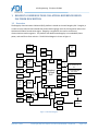
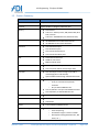
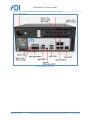
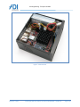
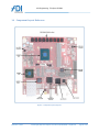
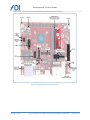
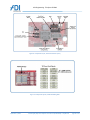
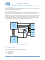
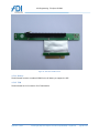
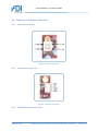
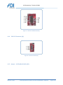
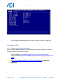
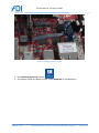
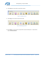
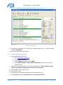
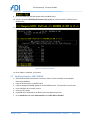
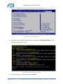
The Open IP ODM
Intel Rangeley Communications Collateral
(RCC) Reference Design Platform
User Manual
Revision: 1.00
ADI Engineering, Inc.
1758 Worth Park
Charlottesville, VA 22911
www.adiengineering.com
Phone: (434)-978-2888
Fax: (434)-978-1803
ADI Engineering: The Open IP ODM
Revision History
Date
Revision
Section
Remarks
06/12/2013
06/24/2013
06/26/2013
07/12/2013
0.01
0.02
0.03
0.04
-
09/03/2013
1.0
-
September 3, 2013
Initial Draft
Initial feedback updates
Remove optional wording for battery
Change temperature specification for Astep silicon
Official release
Intel Rangeley Reference Platform User Manual (45700-0004) – Confidential
page 2 of 42
ADI Engineering: The Open IP ODM
Table of Contents
1
RANGELEY COMMUNICATIONS COLLATERAL REFERENCE DESIGN PLATFORM DESCRIPTION ...................... 4
1.1
OVERVIEW ................................................................................................................................................... 4
1.2
FEATURE SUMMARY ...................................................................................................................................... 5
1.3
ENCLOSURE REFERENCE.................................................................................................................................. 7
1.4
COMPONENT LAYOUT REFERENCE .................................................................................................................. 11
1.5
COMPONENT OVERVIEW .............................................................................................................................. 14
1.5.1 Rangeley SOC ..................................................................................................................................... 14
1.5.2 Memory.............................................................................................................................................. 14
1.5.3 82599ES (Dual 10G Controller) .......................................................................................................... 15
1.5.4 I347-AT4 (Quad GBE PHY) .................................................................................................................. 15
1.5.5 88E1112 (Single GBE PHY) ................................................................................................................. 15
1.5.6 CP2105 (Dual USB-to-UART Bridge) ................................................................................................... 15
1.5.7 SOC EEPROM ...................................................................................................................................... 16
1.5.8 SOC SPI Flash Devices ......................................................................................................................... 16
1.5.9 Management FPGA ............................................................................................................................ 16
1.5.10
PCIe Slot ......................................................................................................................................... 17
1.5.11
Battery ........................................................................................................................................... 18
1.5.12
TPM ............................................................................................................................................... 18
1.6
CONNECTOR AND JUMPER REFERENCE ............................................................................................................ 20
1.6.1 Power Connector (J1) ......................................................................................................................... 20
1.6.2 Fan Connecters (J3 & J2) .................................................................................................................... 20
1.6.3 USB Front Panel Connector (J7) ......................................................................................................... 20
1.6.4 VR12 I2C Connector (J4) ..................................................................................................................... 21
1.6.5 Jumper – 10G Enable/Disable (J32) ................................................................................................... 21
1.6.6 TPM Connector (J11) .......................................................................................................................... 22
1.6.7 In-Circuit SPI Connector (J25) and Jumper (J24) ................................................................................. 22
1.6.8 FPGA JTAG Connector (J22) ................................................................................................................ 23
1.6.9 RS232 UART Connector (J13), PECI Connector (J18), UART/PECI Jumper (J20) ................................. 23
1.6.10
Jumper – 88E1112 CONFIG3 (J23) ................................................................................................. 24
1.6.11
NCSI Connector (J9), Front Panel Connector (J16), NCSI Jumper (J14) ........................................... 24
1.6.12
SMBus Connector (J31), Redundant Boot Jumper (J30) ................................................................ 25
2
RCC SETUP AND USE .................................................................................................................................. 27
2.1
2.2
2.3
2.4
2.4.1
2.4.2
2.5
2.6
2.7
2.7.1
2.7.2
SERIAL PORT DRIVERS .................................................................................................................................. 27
RUNNING YOCTO LINUX ............................................................................................................................... 27
MANAGEMENT CONSOLE.............................................................................................................................. 28
UPDATING BIOS ......................................................................................................................................... 29
Updating Flash with a SPI Programmer ............................................................................................. 29
Updating BIOS from EFI Shell ............................................................................................................. 34
UPDATING RANGELEY GBE EEPROM ............................................................................................................. 36
UPDATING 82599 EEPROM........................................................................................................................ 38
UPDATING MANAGEMENT FPGA .................................................................................................................. 39
Updating FPGA over JTAG .................................................................................................................. 39
Updating FPGA over console .............................................................................................................. 41
3 ....................................................................................................................................................................... 42
September 3, 2013
Intel Rangeley Reference Platform User Manual (45700-0004) – Confidential
page 3 of 42
ADI Engineering: The Open IP ODM
1 RANGELEY COMMUNICATIONS COLLATERAL REFERENCE DESIGN
PLATFORM DESCRIPTION
1.1 Overview
The Rangeley Communications Collateral (RCC) platform is based on the Intel Rangeley SOC. Rangeley is
a multi-core (up to 8) Intel Atom based SOC product featuring high levels of I/O integration and an Intel
QuickAssist hardware acceleration engine. Rangeley is targeted for the routers and security
communications market segment. This platform will demonstrate Rangeley in an embedded, lower
power, and small form factor solution. The RCC block diagram is shown in Figure 1.
SATA
Connector
SATA
Connector
SATA
Connector
mSATA
Drive
eSATA
(x2)
RJ45 w/
Mag
(x3)
USB
Type-A
(x2)
4
I347-AT4
QUAD
PHY
2
SATA
Gen3
SATA
Gen2
72
88E1112
SGMII
PCIe
x8
1G SFP
10G
SFP+
Dual
4
USB
3
SGMII
RJ45 w/
Mag
USB
Header
(x2)
DDR3
Rangeley /
Avoton
SoC
72
DDR3
CH-A 4GB Memory
Down, Dual Rank, x8, w/
ECC
CH-B SODIMM (dual
rank support)
PCIe
x8
x8 PCIe
Slot
JTAG
XDP
NCSI
HEADER
UART
82599ES
10 GbE
LPC
SPI
2
PECI
HEADER
Header
RS232
Mini-B
USB
UART-toUSB
Bridge
TPM
Atom
µServer
Clocks
HEX
DISPLAY
FPGA
BMC
12V
Flash
8 MB
Power
Regulators
Flash
8 MB
Figure 1 - RCC Block Diagram
September 3, 2013
Intel Rangeley Reference Platform User Manual (45700-0004) – Confidential
page 4 of 42
ADI Engineering: The Open IP ODM
1.2 Feature Summary
Feature
Description
Board Form Factor
12-layer Mini-ITX (6.7” X 6.7”)
Processor
Supports all SKU’s of Rangeley and Avoton CPU
Memory
Dual Channel
Channel A – Memory Down, 4GB, DDR3L-1600, Dual
Rank, with ECC
Channel B – SODIMM with ECC (1DPC Dual Rank)
Clocking
IDT 9VRS4420 for Atom-based microservers
IDT 9ZXL0651 for PCIe clock distribution
Hard Drive
Local mSATA Gen3 port
Two eSATA Gen2 ports
One internal SATA Gen3 port
Two internal SATA Gen2 ports
BIOS
Redundant SPI Boot Flash
16MB for main device
8MB for failsafe device
USB
Two back panel USB 2.0 ports
Two front panel USB 2.0 ports (through cable)
SOC UART
One console port to CPU through a mini USB to
UART bridge (Silicon Labs CP2105)
Optional RS232 UART through motherboard header
LAN support
Four 10/100/1000Base-TX Ethernet Ports
o Three per Intel I347-AT4 quad PHY
Controller
o One per Marvell 88E1112 PHY
Two 1G/10G SFP+ Ports per Intel 82599ES controller
One 100/1G SFP per Marvell 88E1112 PHY
Debug Interface
XDP 60-pin debug interface
Expansion Ports
One PCIe x8 Gen2 Slot
TPM Header
Battery
Coin cell battery (CR2032) for RTC
On Board Management
SmartFusion FPGA
o Power Sequencing
nd
o Accessible through 2 UART on CP2105
o Board Option Setting (Redundant SPI, 10G
Power, etc…)
September 3, 2013
Intel Rangeley Reference Platform User Manual (45700-0004) – Confidential
page 5 of 42
ADI Engineering: The Open IP ODM
o
o
o
o
Monitor Critical Signals
PORT80 Display
Fan Management (Future feature)
BMC/IPMI Support (Future feature)
Enclosure
8.9” X 3.5” X 8.3” Steel Enclosure with Aluminum
bezel
Power and Reset Buttons
Power and HDD LED’s
Support for one PCIe Card
Support for two 2.5” HDD
One 80mm fan
Power Supply
Flex ATX Power Supply (Internal to Enclosure)
220W Max
100 - 240 VAC
50 - 60Hz
5-3 Amp
Temperature
Temperature is 20°C to 35°C ambient outside
1
enclosure
1
RCC system operating range for the Alpha silicon stepping, should be within 20°C to 35°C during normal operation.
The operating temperature for future stepping’s is predicted to increase to meet NEBS level 3 qualification
September 3, 2013
Intel Rangeley Reference Platform User Manual (45700-0004) – Confidential
page 6 of 42
ADI Engineering: The Open IP ODM
1.3 Enclosure Reference
Figure 2 - Enclosure Front Panel
September 3, 2013
Intel Rangeley Reference Platform User Manual (45700-0004) – Confidential
page 7 of 42
ADI Engineering: The Open IP ODM
Figure 3 - Enclosure Back Panel
September 3, 2013
Intel Rangeley Reference Platform User Manual (45700-0004) – Confidential
page 8 of 42
ADI Engineering: The Open IP ODM
Figure 4 - Inside Enclosure
September 3, 2013
Intel Rangeley Reference Platform User Manual (45700-0004) – Confidential
page 9 of 42
ADI Engineering: The Open IP ODM
Figure 5 – Enclosure Cover, HDD Mount (HDD not provided with kit)
September 3, 2013
Intel Rangeley Reference Platform User Manual (45700-0004) – Confidential
page 10 of 42
ADI Engineering: The Open IP ODM
1.4 Component Layout Reference
Figure 6 – Component Layout, Major ICs
September 3, 2013
Intel Rangeley Reference Platform User Manual (45700-0004) – Confidential
page 11 of 42
ADI Engineering: The Open IP ODM
Figure 7 - Component Layout, Internal Connectors
September 3, 2013
Intel Rangeley Reference Platform User Manual (45700-0004) – Confidential
page 12 of 42
ADI Engineering: The Open IP ODM
Figure 8 - Component Layout, Internal Connectors (cont)
Figure 9 - Component Layout, Port80 and Debug LEDs
September 3, 2013
Intel Rangeley Reference Platform User Manual (45700-0004) – Confidential
page 13 of 42
ADI Engineering: The Open IP ODM
Figure 10 - Front Panel Connectors
1.5 Component Overview
1.5.1 Rangeley SOC
The RCC system ships with the highest core count SKU of the Rangeley SoC. Please refer to the latest
Intel documentation on the SoC for the SKU features. The RCC system has been designed to be
compatible with all other Rangeley SKUs as well, inclusive of lower core count SKUs.
1.5.2 Memory
The RCC supports two channels of DDR3. These channels are configured as follows:
Channel-A – Is memory down (soldered to board), configured as 4GB, Dual Rank, 1600MT/s,
ECC, 1.35V (18 total devices)
Channel-B – Is a SODIMM. Supported SODIMM is a 4GB, Dual Rank, 1600MT/s, ECC, 1.35V
A requirement of the SOC is that channel-B must be equal to channel-A for density, rank, speed, ECC,
and type (i.e. UDIMM, SODIMM, etc..). The BIOS gets this information by reading and comparing the
SPD EEPROMs for each channel. A SPD EEPROM was placed on the board for channel-A. Channel-A was
routed as a UDIMM to simplify the layout so the starting SPD was based on Micron MT18KSF51272AZ1G6. That SPD was then modified to change the type (byte 0x3 in SPD EEPROM) from a UDIMM (0x2) to
a 72b-SO-UDIMM (0x8). The CRC for the SPD was then recalculated.
The RCC system ships with 8GB of memory. The board could support up to 16GB of memory by
changing the memory down devices, SPD, and SODIMM.
September 3, 2013
Intel Rangeley Reference Platform User Manual (45700-0004) – Confidential
page 14 of 42
ADI Engineering: The Open IP ODM
1.5.3 82599ES (Dual 10G Controller)
The 10Gb Ethernet controller is connected to the SOC with a PCIe x8 Gen2 interface. It provides access
to two SFP+ slots. There is a configuration EEPROM (32KB) which configures the device for SFI with no
management. There is also an optional flash device (currently no used), that could hold an option ROM
for PXE boot.
This device and its surrounding circuits can be completely powered down, by setting a jumper on the
board or configuring the board management setting over the management console.
1.5.4 I347-AT4 (Quad GBE PHY)
The SOC is connected to the Intel I347-AT4 quad PHY over SGMII. It configures the PHY using a
MDC/MDIO interface. Three of the SOC MAC interfaces are connected to this PHY:
SGMII-0
SGMII-2
SGMII-3
The PHY is then connected to an RJ45 with integrated magnetics.
Figure 11 - SoC Ethernet port mapping
1.5.5 88E1112 (Single GBE PHY)
The SOC is connected to the Marvell 88E1112 over SGMII-1. It configures the PHY using a MDC/MDIO
interface. This PHY is connected to an RJ45 with integrated magnetics and to an SFP slot. It supports
Auto Media Detection between the two interfaces2.
1.5.6 CP2105 (Dual USB-to-UART Bridge)
The RCC board has a CP2105 which is a dual USB-to-UART bridge. One UART is connected to the console
port on the SOC and the second UART is connected to the management FPGA.
2
SW Driver is still under development to support Auto Media Detection feature
September 3, 2013
Intel Rangeley Reference Platform User Manual (45700-0004) – Confidential
page 15 of 42
ADI Engineering: The Open IP ODM
1.5.7 SOC EEPROM
The SOC uses an EEPROM to configure the Ethernet MAC interfaces. Please refer to Intel representative
for the latest EEPROM image for the RCC board.
1.5.8 SOC SPI Flash Devices
There are two SPI Flash devices connected to the SOC. There is 16MB device which is used for the main
SPI flash image. It contains a BIOS and descriptor which is used for normal operation and can be
updated with new versions. There is an 8MB device that is used as a failsafe SPI flash image to provide
redundant boot functionality. This device cannot be updated and is used only when the main device
fails. The redundant boot function is controlled by the FPGA and can be enabled/disabled by a jumper
or configuring the board management settings over the management console.
SPI_CLK
Rangeley /
Avoton
SoC
SPI_MOSI
8MB SPI
Flash
SPI_MISO
SPI_CS_N
3.3V
0
1
SOC_FPGA_DATA_OUT
SOC_FPGA_DATA_IN
SOC_FPGA_CLK
0
1
16MB SPI
Flash
SPI_CS_SELECT
FPGA
Figure 12 - Redundant SPI FLash
1.5.9 Management FPGA
The board management FPGA performs the following functions:
Power Sequencing
Redundant SPI
Board Settings
September 3, 2013
Intel Rangeley Reference Platform User Manual (45700-0004) – Confidential
page 16 of 42
ADI Engineering: The Open IP ODM
Analog Measurements (Temperature, Voltage, Current)
Monitors Critical Signals
Manufacturing Information
The FPGA can report status and the user can change settings using the UART connected to the USB-toUART bridge. Refer to section 2.3 for operation details. The hardware could support the following
features with a firmware upgrade:
BMC/IPMI Support
Serial Over LAN
FAN Monitoring and Control
Remote FPGA updates
1.5.10 PCIe Slot
The RCC board has a PCIe x8 expansion card. The chassis supports a full-height, half-length PCIe x16
card. The board is designed to support up to a 75W card3. A x8-to-x16 riser card is supplied with the kit
to mount the card in the enclosure.
3
September 3, 2013
Thermal testing has only been completed with a 15W card.
Intel Rangeley Reference Platform User Manual (45700-0004) – Confidential
page 17 of 42
ADI Engineering: The Open IP ODM
Figure 13 - PCIe x8 to x16 Riser Card
1.5.11 Battery
The RCC board contains a standard CR2032 coin cell battery to support the RTC.
1.5.12 TPM
The RCC board has 2x7 connector for a TPM module.
September 3, 2013
Intel Rangeley Reference Platform User Manual (45700-0004) – Confidential
page 18 of 42
ADI Engineering: The Open IP ODM
Figure 14 - TPM Module
September 3, 2013
Intel Rangeley Reference Platform User Manual (45700-0004) – Confidential
page 19 of 42
ADI Engineering: The Open IP ODM
1.6 Connector and Jumper Reference
1.6.1
Power Connector (J1)
Figure 15 - Connector: Power (J1)
1.6.2
Fan Connecters (J3 & J2)
Figure 16 - Connector: Fan (J3 & J2)
1.6.3
USB Front Panel Connector (J7)
September 3, 2013
Intel Rangeley Reference Platform User Manual (45700-0004) – Confidential
page 20 of 42
ADI Engineering: The Open IP ODM
Figure 17 - Connector: USB Front Panel (J7)
1.6.4
VR12 I2C Connector (J4)
Figure 18 - Connector: VR12 I2C (J4)
1.6.5
Jumper – 10G Enable/Disable (J32)
September 3, 2013
Intel Rangeley Reference Platform User Manual (45700-0004) – Confidential
page 21 of 42
ADI Engineering: The Open IP ODM
Figure 19 - Jumper: 10G Enable/Disable (J32)
1.6.6
TPM Connector (J11)
Figure 20 - Connector: TPM (J11)
1.6.7
In-Circuit SPI Connector (J25) and Jumper (J24)
September 3, 2013
Intel Rangeley Reference Platform User Manual (45700-0004) – Confidential
page 22 of 42
ADI Engineering: The Open IP ODM
Figure 21 - Connector: SPI (J25), Jumper: SPI (J24)
1.6.8
FPGA JTAG Connector (J22)
Figure 22 - Connector: FPGA JTAG (J22)
1.6.9
RS232 UART Connector (J13), PECI Connector (J18), UART/PECI Jumper (J20)
September 3, 2013
Intel Rangeley Reference Platform User Manual (45700-0004) – Confidential
page 23 of 42
ADI Engineering: The Open IP ODM
Figure 23 - Connector: RS232 (J13), PECI (J18), Jumper PECI/RS232 (J20)
1.6.10 Jumper – 88E1112 CONFIG3 (J23)
Figure 24 - Jumper: 88E1112 TWSI Configuration (J23)
1.6.11 NCSI Connector (J9), Front Panel Connector (J16), NCSI Jumper (J14)
September 3, 2013
Intel Rangeley Reference Platform User Manual (45700-0004) – Confidential
page 24 of 42
ADI Engineering: The Open IP ODM
Figure 25 - Connector: NCSI Header (J9), Front Panel (J16), Jumper NCSI/MDIO (J14)
Schematic Signal
NCSI Pin
Direction
NCSI Function
SMB_GBE_CPU_DATA
NCSI_TX_EN
I
SMB_GBE_CPU_CLK
NCSI_CLK_IN
I
SMB_GBE_CPU_ALERT_N
NCSI_CRS_DV
O
GBE_CPU_SDP0_1
NCSI_ARB_IN
I
NCSI_TXD0
NCSI_TXD0
I
NCSI_TXD1
NCSI_TXD1
I
GPIO_CPU_SUS1
NCSI_RXD0
O
GBE_CPU_WOL
NCSI_RXD1
O
NCSI_ARB_OUT
NCSI_ARB_OUT
O
Notes
Table 1 - NCSI Connector
1.6.12 SMBus Connector (J31), Redundant Boot Jumper (J30)
September 3, 2013
Intel Rangeley Reference Platform User Manual (45700-0004) – Confidential
page 25 of 42
ADI Engineering: The Open IP ODM
Table 2 - Connector: Main SMB (J31), Jumper: Redundant Boot (J30)
September 3, 2013
Intel Rangeley Reference Platform User Manual (45700-0004) – Confidential
page 26 of 42
ADI Engineering: The Open IP ODM
2 RCC SETUP AND USE
2.1 Serial Port Drivers
The RCC has a USB-to-UART bridge for the CPU console and FPGA management console. The device
used is a Silicon Labs CP2105. Before connecting the RCC system, the host computer will need to install
drivers for the CP2105. Follow these instructions:
1.
2.
3.
4.
5.
6.
7.
Go to the following address:
http://www.silabs.com/products/interface/usbtouart/Pages/usb-to-uart-bridge.aspx
Select Tools tab.
Select drivers for your OS. For Windows, select CP210x_VCP_Windows.zip
Download and following instructions for installing driver
Use the provided USB Mini-B cable and connect the RCC system console to the host computer
Verify that host computer can see two additional serial ports
The first serial port added to the host computer will connect to the FPGA management console.
The second serial port will connect to the CPU console.
The user will need to use a terminal emulator (i.e. Hyperterminal, PuTTy) to connect to the consoles.
The settings for the terminal should be the following:
Speed = 115,200
Data Bits = 8
Parity = None
Stop Bits = 1
Flow Control = None
Preferred emulation mode is ANSI
2.2 Running Yocto Linux
The RCC system comes with a mSATA drive with a custom Yocto Linux installation and is ready to use out
of the box. For instructions on how to create Yocto Linux with Rangeley patches and drivers, please
refer to Intel documentation.
1. Connect User Interface. Two options:
a. CPU console port over USB-to-UART bridge
b. Graphics Card in PCIe slot, USB Keyboard
2. Connect AC power cable
3. Press power button on front panel.
4. If using the CPU console port, debug messages should be displayed as the BIOS boots. IF using a
graphics card, nothing will be displayed until the BIOS splash screen.
5. Press ESC when requested by the BIOS to enter the BIOS setup screen
September 3, 2013
Intel Rangeley Reference Platform User Manual (45700-0004) – Confidential
page 27 of 42
ADI Engineering: The Open IP ODM
6. Go to Boot menu and verify that Boot Option #1 is set to boot mSATA (i.e. UEFI: M4CT032M4SSD3). If not, change boot option #1 to mSATA.
7. Go to Save & Exit and select Save Changes and Exit
8. System should boot Yocto Linux. Type root when at command prompt. There is no password.
2.3 Management Console
The RCC board has a management console which is connected to the on-board FPGA over the USB-toUART bridge. The initial version of this management console provides board status information to the
user. This console is still under development and will provide the following features in the future:
User configurable settings for on-board jumpers (i.e. Redundant SPI, 10G Power, etc..)
FPGA update over UART
Additional board status (i.e. Information from Rangeley PECI, Manufacturing Information)
More advanced features that are under consideration
BMC/IPMI Support
Serial OverLAN
FAN Monitoring and Control
Instructions to access management console:
1. Follow instructions in section 2.1 for connecting to serial port. Management console is the first
UART.
2. Power on RCC system
3. You should see management console displayed
September 3, 2013
Intel Rangeley Reference Platform User Manual (45700-0004) – Confidential
page 28 of 42
ADI Engineering: The Open IP ODM
Figure 26 - FPGA Management Console
4. You can navigate console with arrow keys and select or toggle an item with the ENTER key.
2.4 Updating BIOS
2.4.1 Updating Flash with a SPI Programmer
Both the 16MB and 8MB SPI flash devices can be updated using an external programmer. The tools
required to update the flash devices are below:
Dediprog SF100 (http://www.dediprog.com/SPI-flash-in-circuit-programming/SF100)
1.27mm Cable Adapter (http://www.dediprog.com/SPI-flash-in-circuit-programming/ISP-CableAdaptor)
Host computer with Windows OS and Dediprog software installed. Dediprog software is located
at (http://www.dediprog.com/SPI-flash-in-circuit-programming/SF100) under Software
Download tab.
SPI Flash binary with descriptor and BIOS. Available from Intel and ADI
September 3, 2013
Intel Rangeley Reference Platform User Manual (45700-0004) – Confidential
page 29 of 42
ADI Engineering: The Open IP ODM
Figure 27 - DediProg SF100 with 1.27mm Adapter
Instructions for updating SPI Flash
1. Turn off power to RCC system. No external power is required for updating SPI flash
2. Remove enclosure cover. Held on by two screws.
3. Set the jumper (J24) to the SPI flash you want accessible to the external programmer. This
example starts with the 8MB device.
Figure 28 - Jumper for SPI Flash programming
4. Connect Dediprog to the RCC board. Pay attention that pin-1 on the board lines up with the redwire on the adapter cable.
September 3, 2013
Intel Rangeley Reference Platform User Manual (45700-0004) – Confidential
page 30 of 42
ADI Engineering: The Open IP ODM
Figure 29 - DediProg connected to board
5. Start DediProg Engineering software:
6. The software should auto detect the flash. Select W25Q64CV for the 8MB device.
September 3, 2013
Intel Rangeley Reference Platform User Manual (45700-0004) – Confidential
page 31 of 42
ADI Engineering: The Open IP ODM
Figure 30 - DediProg Flash Detection, 8MB
7. Select File icon in the tool bar and select the binary file to be programmed into the flash. Select
Raw Binary. Select OK.
Figure 31 - Loading Dediprog SPI File
September 3, 2013
Intel Rangeley Reference Platform User Manual (45700-0004) – Confidential
page 32 of 42
ADI Engineering: The Open IP ODM
8. Select Erase icon in the tool bar to erase flash contents
Figure 32 - DediProg Erase Flash
9. Select Prog icon in the tool bar to write file to flash
Figure 33 - DediProg Program Flash
10. Select Verify icon in the tool bar to compare flash contents with binary file. Verify that tool
reports Checksum Identical.
September 3, 2013
Intel Rangeley Reference Platform User Manual (45700-0004) – Confidential
page 33 of 42
ADI Engineering: The Open IP ODM
Figure 34 - DediProg Verify
11. If updating the 16MB device, set jumper (J24) to 16MB and repeat steps. The device selected
should be N25Q128A13.
12. Disconnect DediProg from RCC board.
2.4.2 Updating BIOS from EFI Shell
1. Download AMI BIOS update utility
a. Go to http://ami.com/support/
b. Select Technical Support
c. Under AMIBIOS, select Aptio, then SUBMIT
d. Select AMIBIOS & Aptio – AMI Firmware Update Utility and follow instructions to
download utility.
2. Place this utility on a USB flash drive along with the BIOS binary. (NOTE: BIOS binary will be
smaller than the 8MB or 16MB images and does not have descriptor).
3. Insert USB flash drive into RCC system.
4. Power on RCC system
5. Press ESC when requested by the BIOS to enter the BIOS setup screen
6. Go to Save & Exit and under Boot Override select UEFI: Built-in EFI Shell
September 3, 2013
Intel Rangeley Reference Platform User Manual (45700-0004) – Confidential
page 34 of 42
ADI Engineering: The Open IP ODM
Figure 35 - BIOS, boot Built-in EFI Shell
7. USB flash drive will be identified as a fs device and labeled as a Removable HardDisk. In this
example, the USB flash drive is fs1.
Figure 36 - Indentify USB flash drive in EFI shell
8. Go to USB flash drive by typing fs1: followed by ENTER
September 3, 2013
Intel Rangeley Reference Platform User Manual (45700-0004) – Confidential
page 35 of 42
ADI Engineering: The Open IP ODM
9. Go to the folder with the BIOS update utility and BIOS binary.
10. Type the command AfuEfix64.efi filename.rom /p /b /n to update the BIOS. (filename.rom is
the BIOS file).
11. Wait for utility to complete. DO NOT CYCLE POWER DURING UPDATE.
Figure 37 - BIOS Update Complete
12. Once update is complete, cycle power.
2.5 Updating Rangeley GbE EEPROM
1. Download the latest Intel Network Connection Tools from the Intel Business Portal (IBP)
(Document #348742).
2. Copy the EFIx64 tools to a USB flash drive
3. Copy the Rangeley EEPROM update file to the USB flash drive. File should be in test format.
4. Insert USB flash drive into RCC system.
5. Power on RCC system
6. Press ESC when requested by the BIOS to enter the BIOS setup screen
7. Go to Save & Exit and under Boot Override select UEFI: Built-in EFI Shell
September 3, 2013
Intel Rangeley Reference Platform User Manual (45700-0004) – Confidential
page 36 of 42
ADI Engineering: The Open IP ODM
Figure 38 - BIOS, boot Built-in EFI Shell
8. USB flash drive will be identified as an fs device and labeled as a Removable HardDisk. In this
example, the USB flash drive is fs1.
Figure 39 - Indentify USB flash drive in EFI shell
9. Go to USB flash drive by typing fs1: followed by ENTER
September 3, 2013
Intel Rangeley Reference Platform User Manual (45700-0004) – Confidential
page 37 of 42
ADI Engineering: The Open IP ODM
10. Go to the folder with the eeupdate64e.efi update utility and EEPROM text file.
11. Type eeupdate64e.efi followed by ENTER
Figure 40 - eeupdate64e.efi Adapter Identification
12. Rangeley ports are identified by Vendor-Device 8086-1F41. To update the Rangeley EEPROM,
one of its NICs should be selected in the update command. Below is an example of the update
command.
13. Wait for command to complete and verify it reports successful. DO NOT CYCLE POWER DURING
UPDATE.
2.6 Updating 82599 EEPROM
1. Follow steps 1 through 11 for updating Rangeley EEPROM
2. 82599 ports are identified by Vendor-Device 8086-10FB. To update the 82599 EEPROM, one of
its NICs should be selected in the update command. Below is an example of the update
command.
3. Wait for command to complete and verify it reports successful. DO NOT CYCLE POWER DURING
UPDATE.
September 3, 2013
Intel Rangeley Reference Platform User Manual (45700-0004) – Confidential
page 38 of 42
ADI Engineering: The Open IP ODM
2.7 Updating Management FPGA
2.7.1 Updating FPGA over JTAG
The Management FPGA can be updated over JTAG. The tools required to update the FPGA over JTAG
are below:
Microsemi FlashPro4 programmer (http://www.microsemi.com/fpga-soc/designresources/programming/flashpro#overview)
Host computer with Windows OS and FlashPro software installed.
(http://www.microsemi.com/fpga-soc/design-resources/programming/flashpro#downloads)
FPGA bitfile. Provided from Intel and ADI in the form of .stp file.
Instructions:
1. Turn off power to RCC system.
2. Remove enclosure cover. Held on by two screws.
3. Connect FlashPro4 adapter to RCC system
Figure 41 - Connect FlashPro4 Cable
4. Turn on power to RCC system
September 3, 2013
Intel Rangeley Reference Platform User Manual (45700-0004) – Confidential
page 39 of 42
ADI Engineering: The Open IP ODM
5. Open FlashPro program
6. Select New Project button
Figure 42 - FlashPro New Project
7. Enter name for new project and select location. Single device should be selected.
Figure 43 - FlashPro New Project Name
8. Select Configuration->Load Programming File
September 3, 2013
Intel Rangeley Reference Platform User Manual (45700-0004) – Confidential
page 40 of 42
ADI Engineering: The Open IP ODM
Figure 44 - FlashPro, Load Programming File
9. Select PROGRAM button.
10. Wait for program to Erase, Program, and then Verify update
Figure 45 - FlashPro FPGA Update Complete
11. Disconnect FlashPro4 programmer
12. Power cycle RCC system
2.7.2 Updating FPGA over console
This is a future feature not currently supported.
September 3, 2013
Intel Rangeley Reference Platform User Manual (45700-0004) – Confidential
page 41 of 42
ADI Engineering: The Open IP ODM
3 SUPPORT
Support related to the RCC system (i.e. Hardware, BIOS, Firmware, etc..) will be provided by ADI
Engineering. Each kit comes with a standard support package which includes free technical support (up
to 3 hours) from the engineering team and unlimited access to ADI’s web-based support forums and
download site.
Some customers may need extra support to handle hardware or software development tasks such as
system-level design issues when integrating an ADI product into a larger system (thermal, regulatory,
mechanical, etc.), software porting, debug or testing efforts, or design customization. Customers may
also require design review or consulting services to quickly ramp up their engineering and
manufacturing teams. For these customers ADI offers a variety of support packages to meet their
specific requirements.
Support Package
Key Features
ADI Part
Number
Standard
Development Kit
Support
90 day standard kit warranty
Unlimited access to ADI’s web-based support site
Phone & Email Support during warranty and support period (3 business day response)
Up to 3 hours of support problem solving during the support period
DKSS
Premium
Development Kit
Support
Extends product warranty and support period to 1 year
Unlimited access to ADI’s web-based support site
Phone & Email Support during warranty and support period (1 business day response)
Up to 40 hours of support problem solving and hardware/software engineering assistance during
the support period
DKPS-040
Up to 8 hours of support problem solving and engineering assistance over 1 year
HSP-008
Up to 16 hours of support problem solving and engineering assistance over 1 year
HSP-016
Up to 40 hours of support problem solving and engineering assistance over 1 year
HSP-040
Up to 100 hours of support problem solving and engineering assistance over 1 year
HSP-100
Up to 400 hours of support problem solving and engineering assistance over 1 year
HSP-400
Up to 1000 hours of support problem solving and engineering assistance over 1 year
HSP-1000
Hourly Support
Packages
Table 3 - ADI Support Plans
For questions related to the Intel SoC silicon, please contact your Intel representative.
September 3, 2013
Intel Rangeley Reference Platform User Manual (45700-0004) – Confidential
page 42 of 42