1
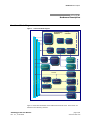
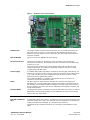
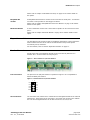
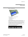
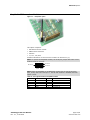
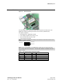
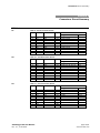
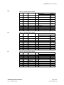
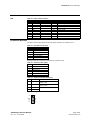
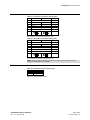
AVR Playground
User Manual
Board Rev.:
Document Rev.:
Revision Date:
2.1
2.1
01.06.2005
Copyright © 2005 by Elektronik-Atelier Kallen
Ch-3075 Rüfenacht / Switzerland
www.avrcard.com
About the Playground Board
Contents
Revision History.................................................................................. 4
Web Site ........................................................................................... 4
Copyright .......................................................................................... 4
About the Playground Board
5
Application......................................................................................... 5
Main Features..................................................................................... 5
Additional Resources ........................................................................... 5
Getting started
6
Your First Steps .................................................................................. 6
Hardware Description
7
Functional Block Diagram ..................................................................... 7
Onboard options ................................................................................. 8
Expansion modules ............................................................................. 9
Header Connectors.............................................................................. 9
Board Configuration
11
Jumper Settings................................................................................ 11
AVRcard Core Module ........................................................................ 12
DC Power Supply .............................................................................. 13
Onboard Options
14
LCD Module and Keys ........................................................................ 14
EasyRadio RF Transceiver Module ........................................................ 15
Bluetooth Module .............................................................................. 16
Expansion Modules
17
Host Interface .................................................................................. 17
Mechanical Data ............................................................................... 19
Serial Busses
20
I2C................................................................................................. 20
I2C Slave Adresses ........................................................................... 21
SPI ................................................................................................. 21
Circuit Diagrams
22
Connectors Pinout Summary
23
CPU Ports ........................................................................................ 23
Address Lines ................................................................................... 25
Expansion Modules ............................................................................ 25
Serial Ports ...................................................................................... 26
DC Power ........................................................................................ 26
References
27
Product References ........................................................................... 27
Other References .............................................................................. 27
Revision History................................................................................ 27
Contact ........................................................................................... 28
Notice to Users
AVR Playground User Manual
Rev. 2.1, 01.06.2005
29
page 2/29
www.avrcard.com
About the Playground Board
Figures
Figure 1 – Functional Block Diagram .............................................................. 7
Figure 2 – Hardware Layout and Placement..................................................... 8
Figure 3 – Pin 1 Position on I/O Port Headers .................................................. 9
Figure 3 - General Pinout of I/O Port Headers.................................................. 9
Figure 4 – A0-7 Connector Pinout ................................................................ 10
Figure 5 – Expansion modules select signals ................................................. 10
Figure 6 – Expansion modules interrupt signals ............................................. 10
Figure 7 – Jumper locations........................................................................ 11
Figure 8 – Reset pin.................................................................................. 12
Figure 9 – LCD and keys option .................................................................. 14
Figure 10 – EasyRadio option ..................................................................... 15
Figure 11 – Bluetooth option ...................................................................... 16
Figure 12 – Expansion Modules Locations ..................................................... 17
Figure 13 – Expansion module connector pinout ............................................ 17
Figure 14 – Mechanical dimensions of expansion modules ............................... 19
Figure 13 – Expansion module connector pinout ............................................ 25
Tables
Table 1 - Jumper Settings .......................................................................... 11
Table 2 – AVRcard Connectors .................................................................... 12
Table 3 – Battery Connector Pinout ............................................................. 13
Table 4 – External Power Connector Pinout (X8) ............................................ 13
Table 5 – Port signals used for LCD module................................................... 14
Table 5 – Port signals used for EasyRadio module .......................................... 15
Table 6 – Port signals used for Bluetooth module ........................................... 16
Table 7 – I2C addresses ............................................................................ 21
Table 8 – Port A Connector Pinout ............................................................... 23
Table 9 – Port B Connector Pinout ............................................................... 23
Table 10 – Port C Connector Pinout ............................................................. 23
Table 11 – Port D Connector Pinout ............................................................. 24
Table 12 – Port E Connector Pinout.............................................................. 24
Table 13 – Port F Connector Pinout.............................................................. 24
Table 14 – A0-7 Connector Pinout ............................................................... 25
Table 15 – SPI Select Lines (X17) ............................................................... 25
Table 16 – Interrupt Lines (X18) ................................................................. 25
Table 17 – Expansion Module Connectors ..................................................... 25
Table 18 – Serial Port 1 Connector Pinout (X10) ............................................ 26
Table 19 – Serial Port 2 Connector Pinout (X11) ............................................ 26
Table 20 – DC Power Connector Pinout (X8).................................................. 26
AVR Playground User Manual
Rev. 2.1, 01.06.2005
page 3/29
www.avrcard.com
About the Playground Board
Revision History
The revision history is shown in Section References on page 27
Web Site
This manual can also be found on the website www.avrcard.com.
Copyright
Information in this document is subject to change without prior notice in order to
improve reliability, design and function and does not represent a commitment on
the part of the manufacturer. In no event will the manufacturer be liable for direct,
indirect, special, incidental, or consequential damages arising out of the use or
inability to use the product or documentation, even if advised of the possibility of
such damages.
This document contains proprietary information protected by copyright. All rights
are reserved. No part of this manual may be reproduced by any mechanical,
electronic, or other means in any form without prior written permission of the
manufacturer.
All product names referenced herein are trademarks of their respective companies.
AVR Playground User Manual
Rev. 2.1, 01.06.2005
page 4/29
www.avrcard.com
About the Playground Board
Section 1
About the Playground Board
The AVR Playground is a base board for the AVRcard Microcontroller Core Module. It provides easy connection
options, and a number of additional features.
Application
Development platform for AVR (ATmega128) based solutions
Education platform
Platform for functional prototypes
Plug-in AVRcard with Atmega128 processor
Plug-in expansion modules on I2C and SPI bus
Plug-in EasyRadio RF transceiver module
Plug-in Class 1 Bluetooth module
Plug-in 16x3 character LCD on SPI bus
6 pushbuttons on I2C port expander
Piezo speaker
Voltage regulator, allows for use of inexpensive power supply
Standard RJ-45 connectors for both RS-232 and the RS-485 interfaces
Main Features
CPU ports routed to headers with STK500 compatible pinout
Address bus demultiplexed
32Kbytes SRAM
Euro card size (100 x 160mm)
Additional Resources
Product Information – All updated product information can be retrieved at the
product web site, www.avrcard.com.
Application Support – Please check the Resources pages regularly at
www.avrcard.com for design notes and application hints. Further support is
available by email from [email protected].
Custom Designs – Custom population or customized versions of the product are
available. For inquiries please contact [email protected].
AVR Playground User Manual
Rev. 2.1, 01.06.2005
page 5/29
www.avrcard.com
Getting started
Section 2
Getting started
Your First Steps
Prerequisites for
Operation
Installation
The following hardware items are necessary to run the Playground board:
A standard PC equipped with Linux or Windows 95/98/NT/2000 and an available
serial COM port.
Terminal emulation software, such as Hyperterminal.
An unregulated power supply matching your local mains. It should supply DC 816V, 200 mA minimum, on a a EIAJ Standard JSAP3 connector.
Remove the board from the antistatic bag. Visually inspect the board to verify that
it was not damaged during shipment.
WARNING: As with all computer equipment, the Playground board may be severely
damaged by electrostatic discharge (ESD). Be sure to take proper precautions
before removing the Playground board from the anti-static bag.
1. Set jumpers according to the application’s requirement. Refer to Board
Configuration on page 11 for details.
2. If you purchased the Playground separately from the AVRcard core module,
insert the AVRcard. See instructions on page 12.
3. If you want to add on-board options, please refer to Section Onboard Options
from page 14 in this manual.
4. If you want to add expansion modules, please refer to Section Expansion
Modules from page 17 in this manual and to the respective module datasheet.
5. Connect serial cable on X10 (Serial port 1) and to an available COM port on the
PC. Start a terminal program, use the communications parameters:
9600bps, 8 databits, 1 stopbit, no parity, no handshake.
6. Connect the power cable to a DC power supply of 9-12V.
Operation
1. Switch on power. The red LED D1 will lit.
2. On the terminal appears the welcome message of the AVRcard monitor. Refer
to [1] for a description of the available monitor commands and features.
AVR Playground User Manual
Rev. 2.1, 01.06.2005
page 6/29
www.avrcard.com
Hardware Description
Section 3
Hardware Description
Functional Block Diagram
ATmega128
RTC
Reset
Demux
RS-232
Driver
32KB SRAM
TWI Bus
SPI Bus
SerPort1
Port Bus
RS-485
Driver
RS-232/485
Connector
RS-232
Connector
Port
Connectors
I2C Port
Expander
FRAM
5V/3.3V
Level Shifter
Connectivity
Debug
Interface
EasyRadio
Transceiver
Bluetooth
Module
Keys, LEDs
Options
Programming
Interface
AVRcard Core Module
Figure 1 – Functional Block Diagram
LCD
Expansion
Modules
Figure 2 shows the baseboard and its different functional areas. These areas are
detailed in the following sections.
AVR Playground User Manual
Rev. 2.1, 01.06.2005
page 7/29
www.avrcard.com
Hardware Description
Figure 2 – Hardware Layout and Placement
AVRcard slot
Two 32-pin headers connect to power and ports. A 1-pin header connects to the
CPU reset signal, as there is no reset signal on the standard connectors of the
AVRcard. The reset signal is used in conjunction with the TCP/IP module and the
expansion modules.
TCP/IP Module
This slot receives the IIM7010 Ethernet module.
RS-232 connectors
Two RJ-45 connectors are provided for easy connection to the two RS-232
interfaces of the AVRcard. Pin assignment of each connector can be configured by
jumpers (J13, J15).
The second RJ-45 connector also carries the RS-485 signals and the DC input
voltage of the board. This voltage is enabled by Jumper J2 and can be used to
remotely power RS-485 nodes.
Power supply
A standard 7805 voltage regulator is provided for the 5V supply. Alternatively, a 2
Watt DC-DC converter can be used to provide an increased DC input voltage range
(e.g. 9-18V, 18-36V). DC power is applied through the power jack J8. A diode
protects the circuit against false polarity.
For the Ethernet-Module, a separate 3.3V regulator is used. A second 3.3V
regulator is used for the Bluetooth module.
Reset
The Reset signal is routed from the AVRcard core module to the Playground
baseboard via a one-pin header that connects to the bottom of the ISP header on
the AVRcard. For the IIM7010A Ethernet adapter, the reset signal is also inverted
by U11 (74HC04). The active low reset is distributed to all expansion modules and
the Bluetooth module.
External SRAM
The Playground contains a footprint for a 28-pin DIP socket (U3) where an external
SRAM device can be mounted. Make sure the SRAM device has the same voltage
range as the rest of the design.
Onboard options
LCD and Pushbutton
keys
A small alphanumeric LCD (3 lines, 16 characters) can be mounted across the lower
expansion module area (J25). The connector pinout is designed for the EA DOG-M
module from Electronic Assembly. It is connected to the SPI bus.
A PCF8574 I2C port expander allows for the connection of 6 pushbuttons and 2
LEDs.
AVR Playground User Manual
Rev. 2.1, 01.06.2005
page 8/29
www.avrcard.com
Hardware Description
Please refer to chapter “LCD Module and Keys” on page 14 for further details on
this option.
EasyRadio RF
module
An EasyRadio RF transceiver module can be connected to serial port 1. An antenna
connector is also provided on the Playground board.
Please refer to chapter “EasyRadio RF Transceiver Module” on page 15 for further
details on this option.
Bluetooth Module
A class 1 bluetooth module with a serial channel profile can be connected to serial
port 1.
Please refer to chapter “Bluetooth Module” on page 16 for further details on this
option.
Expansion modules
The AVR Playground provides 4 slots for additional minimodules. These small formfactor modules connect via the TWI or the SPI interface and provide specific
connectivity and i/o functions.
For more details, refer to Section “Expansion Modules” on page 17.
Header Connectors
All CPU ports and some additional signals can be connected by standard 0.1”
headers. Pin 1 of each header has a square pad.
Figure 3 – Pin 1 Position on I/O Port Headers
Port Connectors
The pinout for the I/O port headers is explained in Figure 4. It is compatible to
Atmel’s STK500 port headers.
Figure 4 - General Pinout of I/O Port Headers
1
2
Px0
Px1
Px2
Px3
Px4
Px5
Px6
Px7
GND
VCC
PORTx
A0-7 Connector
The connector X20, marked A0-7 contains the 8 least-significant bits of the external
address bus. The purpose of the connector is to provide easy access to the address
bus. The 8 most significant bits can be found on the Port C connector X4.
AVR Playground User Manual
Rev. 2.1, 01.06.2005
page 9/29
www.avrcard.com
Hardware Description
Figure 5 – A0-7 Connector Pinout
1
2
A0
A1
A2
A3
A4
A5
A6
A7
GND
VCC
A0-7
Expansion module
select signals
Figure 6 – Expansion modules select signals
1
2
SEL1
SEL2
SEL3
SEL4
SEL5
BEEPER
SEL5 is connected to the CS signal of the on-board LCD.
BEEPER is connected to the on-board piezo speaker. This speaker can be connected
to any port to deliver audible signals.
Expansion module
interrupt signals
Figure 7 – Expansion modules interrupt signals
1
2
INT1
INT2
INT3
INT4
INT5
INT6
INT5 is connected to the INT signal of the Ethernet module.
INT6 is connected to the INT signal of the on-board I2C port expander used for the
pushbutton switches.
AVR Playground User Manual
Rev. 2.1, 01.06.2005
page 10/29
www.avrcard.com
Board Configuration
Section 4
Board Configuration
Jumper Settings
Figure 8 – Jumper locations
Table 1 - Jumper Settings
No.
Description
Status
open
short
J13
SerPort1
TXD
Pin 2
TXD
J15
SerPort2
Pin 3
RXD
Pin 3
Pin 2
RXD
1
1
For crossover serial cable
For straight serial cable
J2
Ext Pwr
No power on pin 1 of X11
DC input power on pin 1 of X11
J9
Pwr
Board not powered by on-board
voltage regulator
+5V power applied to board
J1
RSSI
RSSI Output of EasyRadio
module connected to ADC7
N.C.
XRAM
CS of SRAM connected to A15
J14
1
CS of SRAM pulled high
The RXD and TXD signals can be interchanged on each of the RJ45 connectors, as
shown in the table.
Jumpers are standard (0.1").
Note: The SRAM is disabled by default. To enable SRAM support, put a jumper on
J14. The SRAM occupies the memory space from $1000-$7FFF.
1
Please note that on the AVRcard core module, A15 (PC7) is also used as an enable signal for
the RS-485 driver.
AVR Playground User Manual
Rev. 2.1, 01.06.2005
page 11/29
www.avrcard.com
Board Configuration
AVRcard Core Module
To fit the AVRcard core module, you must solder the following 0.1” headers face
down to the AVRcard:
Table 2 – AVRcard Connectors
Connector
Fits to
Description
X4
Pin count
32
U4
CPU ports
X5
32
U4
CPU ports, RS-232
X7
4
U4
RS-485
The Reset signal is taken from the ISP header (X2, pin 5). The pin is pushed a few
millimeters to the bottom of the board.
Figure 9 – Reset pin
AVR Playground User Manual
Rev. 2.1, 01.06.2005
page 12/29
www.avrcard.com
Board Configuration
DC Power Supply
The complete logic of the Playground board is driven by a single 5V power supply.
It can be powered from the following sources:
Battery Operation
Battery with 2…5V
External DC power, using a linear voltage regulator
External DC power, using a switching voltage regulator.
The battery is connected to X1 on the AVRcard. As shown in Table 3. The on-board
power switch is inactive in this configuration.
The step-up DC converter on the AVRcard is capable of delivering 250mA at 5V.
Please refer to [1].
Note: Make sure the jumper J9 is be left open in this configuration.
Table 3 – Battery Connector Pinout
Pin
External Power,
Linear Regulator
Function
Description
1
BATT+
+2..5V battery power input
2
BATT-
0V battery (GND)
3
/LOWBATT
is pulled low if battery voltage drops below 1.3V
In this (default) configuration, an 7805 regulator is used to supply the 5V to the
board. It is fitted with a 15K/W heatsink.
Power shall be applied through a EIAJ Standard JSAP3 plug to X8:
Table 4 – External Power Connector Pinout (X8)
Pin
Function
inner
PWR -
outer
PWR +
The jumper J9 must be closed in order to route 5V supply to the board.
External Power,
Switching Regulator
As an option, a 2 Watt DC-DC converter can be soldered in place of the linear
regulator. With this, a wider input voltage range can be achieved. A datasheet of a
suitable DC converter can be found in [7].
Power shall be applied through a EIAJ Standard JSAP3 plug to X8, as shown above.
The jumper J9 must be closed in order to route 5V supply to the board.
AVR Playground User Manual
Rev. 2.1, 01.06.2005
page 13/29
www.avrcard.com
Onboard Options
Section 5
Onboard Options
LCD Module and Keys
Figure 10 – LCD and keys option
This option comprises the following components:
LCD module (U6)
PCF8574 I2C port expander (U14)
6 pushbuttons SW1-6
2 LEDs, R7, R8
R5, R6, R10-15, R19
The LCD is connected to the SPI bus. In addition to the MOSI and SCK lines, it uses
PB4 for the Register Select (RS) signal. Please refer to [6] for details on the
operation of the LCD. The select (CS5) must be jumpered to an available CPU port.
Display contrast is adjusted by software. R4 sets the background LED current.
The pushbutton switches can be read via the I2C port expander, they are active
low. Alternatively, LEDs can be used in place of a switch, as the PCF8574 is able to
source 20mA on each output. Refer to the PCF8574 datasheet in [4].
The PCF8574 provides an interrupt line which is routed to INT6 (X18). This line is
pulled low on each level change on the input ports.
Table 5 – Port signals used for LCD module
Port
Function
PB1
SCK
PB2
MOSI
O
PB4
RS
O
AVR Playground User Manual
Rev. 2.1, 01.06.2005
I/O
Comments
O
page 14/29
www.avrcard.com
Onboard Options
EasyRadio RF Transceiver Module
Figure 11 – EasyRadio option
This option comprises:
ER-TRS transceiver module
SMA antenna connector
Antenna
L1, C11, C12, R20
Detailed information on the transceiver module can be found in [7].
Note: To operate the EasyRadio module, the serial port jumper RX1 select on the
AVRcard must be removed:
RX2 select
RX1 select
TX2 select
1
RS232
RS485
Note: Either the EasyRadio or the Bluetooth module may be used at the same
time, as they share the serial port 1. The RS-232 interface is disabled when this
option is used.
Table 6 – Port signals used for EasyRadio module
Port
Function
PD4
PD5
PE0
PE1
PF7
RTS
CTS
TXD
RXD
RSSI
AVR Playground User Manual
Rev. 2.1, 01.06.2005
I/O
O
I
I
O
I
Comments
Via R20
Via jumper J1
page 15/29
www.avrcard.com
Onboard Options
Bluetooth Module
Figure 12 – Bluetooth option
The Promi-ESD class 1 Bluetooth module [8] is connected to serial port 1 and
additional control lines through a 3V/5V level converter (74VHC08, U8).
This option comprises:
Promi-ESD class 1 Bluetooth module
3.3V voltage regulator U12 with C4, C10
Level converter U8, R16, R17, R18
10-pin female header M5
Note: To operate the Bluetooth module, the serial port jumper RX1 select on the
AVRcard must be removed:
RX2 select
RX1 select
TX2 select
1
RS232
RS485
Note: Either the EasyRadio or the Bluetooth module may be used at the same
time, as they share the serial port 1. The RS-232 interface is disabled when this
option is used.
Table 7 – Port signals used for Bluetooth module
Port
Function
PD4
PD5
PD6
PD7
PE0
PE1
CTS
RTS
DCD
DSR
TXD
RXD
AVR Playground User Manual
Rev. 2.1, 01.06.2005
I/O
O
I
I
O
I
O
Comments
Via R18
page 16/29
www.avrcard.com
Expansion Modules
Section 6
Expansion Modules
Figure 13 – Expansion Modules Locations
Host Interface
Two serial interfaces are supported by the modules: SPI and I2C. For modules with
an onboard AVR controller, the SPI is also used as a programming interface for the
firmware.
Pinout of the Host
Interface Header
The host controller is connected via an 10-pin header with 0.1” spacing.
Figure 14 – Expansion module connector pinout
1
2
+5V
SS
SCK
MOSI
MISO
GND
RES
INT
SCL
SDA
I2C Interface
SCL (Pin 9):
Serial Clock line – the signal used to synchronize communication between the
master and the slave.
SDA (Pin 10):
Serial Data line – the signal used to transfer data between the transmitter and the
receiver.
Pull-up Resistors
There is a 2.7K resistor on each I2C line (SCL, SDA). The lines are effectively pulled
up to 5V, so that results in approximately 1.8 mA of pull-up current. If the
Playground is connected to an I2C bus that also includes pull-up resisters, the total
pull-up current could be up to a total of 3 mA. (The I2C specification allows for a
AVR Playground User Manual
Rev. 2.1, 01.06.2005
page 17/29
www.avrcard.com
Expansion Modules
maximum of 3 mA pull-up current on each I2C line.) As long as downstream I2C
devices can sink more than 5 mA of current, the protocol should operate properly.
SPI Interface
SCK (Pin 3):
Serial Clock – control line that is driven by the master and regulates the flow of the
data bits.
MOSI (Pin 4):
Master Out Slave In – this data line supplies output data from the master which is
shifted into the slave.
MISO (Pin 5):
Master In Slave Out – this data line supplies the output data from the slave to the
input of the master.
SS (Pin 2):
Slave Select – control line that allows slaves to be turned on and off via hardware
control.
When the SPI interface is activated as a master, the slave select line (SS) will
actively driven low by the appropriate firmware driver. The MOSI and SCK lines are
driven as appropriate for the SPI mode. After the master transmission is complete,
these lines shall be returned to a high impedance state in order for the Playground
to be then reconnected to another SPI environment as a slave.
Consequently, any SPI slave target to which the Playground is interfaced must have
a pull-up resistor on its slave select line, preventing fluttering of the voltage when
the Playground stops driving the signal.
It is also advisable that every slave also have passive pull-ups on the MOSI and
SCK lines. These pull-up resistors can be relatively weak – 100k should be
adequate. As a slave, the MOSI, SCK, and SS lines are configured as an input and
the MISO line is configured as an output.
Control Lines
RES (Pin 7)
On the Playground, this pin is connected to the CPU reset line, which is a push-pull
output. Consequently, the reset line of all modules are activated at the same time
on power-up or manual reset.
INT (Pin 8)
This pin is routed to X18, from where it can be jumpered to one of the external
interrupt inputs of the ATmega128 (INT4-7 on X6).
AVR Playground User Manual
Rev. 2.1, 01.06.2005
page 18/29
www.avrcard.com
Expansion Modules
Mechanical Data
Figure 15 – Mechanical dimensions of expansion modules
AVR Playground User Manual
Rev. 2.1, 01.06.2005
Dimensions: mil
Mounting holes 3.2mm diameter
Mounting holes on application connector side are connected to ground of
module.
Mounting holes on host interface side are isolated
Top view (components side)
page 19/29
www.avrcard.com
Serial Busses
Section 7
Serial Busses
I2C
History
When connecting multiple devices to a microcontroller, the address and data lines
of each devices were conventionally connected individually. This would take up
precious pins on the microcontroller, result in a lot of traces on the PCB, and
require more components to connect everything together. This made these systems
expensive to produce and susceptible to interference and noise.
To solve this problem, Philips developed Inter-IC bus, or I2C, in the 1980s. I2C is a
low-bandwidth, short distance protocol for on board communications. All devices
are connected through two wires: serial data (SDA) and serial clock (SCL).
Because all commnication takes place on only two wires, all devices must have a
unique address to identify it on the bus. Slave devices have a predefined address,
but the lower bits of the address can be assigned to allow for multiples of the same
devices on the bus.
Theory of Operation
I2C has a master/slave protocol. The master initiates the communication. The
sequence of events are:
1. The master device issues a start condition. This condition informs all the
slave devices to listen on the serial data line for their respective address.
2. The master device sends the address of the target slave device and a
read/write flag.
3. The slave device with the matching address responds with an
acknowledgment signal.
4. Communication proceeds between the master and the slave on the data
bus. Both the master and slave can receive or transmit data depending on
whether the communication is a read or write. The transmitter sends 8-bits
of data to the receiver which replies with a 1-bit acknowledgment.
5. When the communication is complete, the master issues a stop condition
indicating that everything is done.
Regardless of how many slave units are attached to the I2C bus, there are only two
signals connected to all of them. Consequently, there is additional overhead
because an addressing mechanism is required for the master device to
communicate with a specific slave device.
Features
I2C has many features other important features worth mentioning. It supports
multiple data speeds: standard (100 kbps), fast (400 kbps) and high speed (3.4
Mbps) communications.
Other features include:
_
_
_
_
Built in collision detection,
10-bit Addressing,
Multi-master support,
Data broadcast (general call).
For more information about other features, look at the references at the end of this
section.
Benefits and
Drawbacks
Since only two wires are required, I2C is well suited for boards with many devices
connected on the bus. This helps reduce the cost and complexity of the circuit as
additional devices are added to the system.
Due to the presence of only two wires, there is additional complexity in handling
the overhead of addressing and acknowledgments.
AVR Playground User Manual
Rev. 2.1, 01.06.2005
page 20/29
www.avrcard.com
Serial Busses
I2C Slave Adresses
The following devices are connected to the TWI bus. The Atmega128 is configured
as master, the other devices are slaves.
Note that the addresses below contain the R/W bit.
Table 8 – I2C addresses
Slave address
assignments
Address
Device
Function
Ref.
0x50
FeRAM
Nonvolatile RAM, on AVRcard
0x68
RTC
Realtime clock, on AVRcard
0x21
Port expander
Pushbutton keys, LEDs
U14
0x7F
IIM7010A Module
TCP/IP over Ethernet connectivity
U9
2
SPI
History
SPI is a serial communication bus developed by Motorola. It is a full-duplex protocol
which functions on a master-slave paradigm that is ideally suited to data streaming
applications.
Theory of Operation
SPI requires four signals: clock (SCLK), master output/slave input (MOSI), master
input/slave output (MISO), slave select (SS). Three signals are shared by all
devices on the SPI bus: SCLK, MOSI and MISO. SCLK is generated by the master
device and is used for synchronization. MOSI and MISO are the data lines. The
direction of transfer is indicated by their names. Data is always transferred in both
directions in SPI, but an SPI device interested in only transmitting data can choose
to ignore the receive bytes. Likewise, a device only interested in the incoming bytes
can transmit dummy bytes.
Each device has its own SS line. The master pulls low on a slave's SS line to select
a device for communication. The exchange itself has no pre-defined protocol. This
makes it ideal for data-streaming applications. Data can be transferred at high
speed, often into the range of the tens of megahertz. The flipside is that there is no
acknowledgment, no flow control, and the master may not even be aware of the
slave's presence.
Modes
Although there is no protocol, the master and slave need to agree about the data
frame for the exchange. The data frame is described by two parameters: clock
polarity (CPOL) and clock phase (CPHA). Both parameters have two states which
results in four possible combinations. These combinations are shown in the above
table.
Benefits and
Drawbacks
SPI is a very simple communication protocol. It does not have a specific high-level
protocol which means that there is almost no overhead. Data can be shifted at very
high rates in full duplex. This makes it very simple and efficient in a single master
single slave scenario. Because each slave needs its own SS, the number of traces
required is n+3, where n is the number of SPI devices. This means increased board
complexity when the number of slaves is increased.
2
Part reference designator, see schematic diagram in section Circuit Diagrams on page 22.
AVR Playground User Manual
Rev. 2.1, 01.06.2005
page 21/29
www.avrcard.com
Circuit Diagrams
Section 8
Circuit Diagrams
The diagrams on the following pages are also availabe in a separate document.
AVR Playground User Manual
Rev. 2.1, 01.06.2005
page 22/29
www.avrcard.com
Connectors Pinout Summary
Section 9
Connectors Pinout Summary
CPU Ports
X1
Table 9 – Port A Connector Pinout
Pin
Function
Alt. Function
I/O
Internal Connections
Playground
1
2
3
4
5
6
7
8
9
10
X3
AD0
AD1
AD2
AD3
AD4
AD5
AD6
AD7
I/O
I/O
I/O
I/O
I/O
I/O
I/O
I/O
PWR
PWR
U3/D0,
U3/D1,
U3/D2,
U3/D3,
U3/D4,
U3/D5,
U3/D6,
U3/D7,
AVRcard
U2/1D
U2/2D
U2/3D
U2/4D
U2/5D
U2/6D
U2/7D
U2/8D
Table 10 – Port B Connector Pinout
Pin
1
2
3
4
5
6
7
8
9
10
X4
PA0
PA1
PA2
PA3
PA4
PA5
PA6
PA7
GND
VCC
Function
PB0
PB1
PB2
PB3
PB4
PB5
PB6
PB7
GND
VCC
Alt. Function
SS
SCK
MOSI
MISO
OC0
OC1A
OC1B
OC2
I/O
I/O
I/O
I/O
I/O
I/O
I/O
I/O
I/O
PWR
PWR
Internal Connections
Playground
AVRcard
U6/D6, M1, M2, M3, M4
U6/D7, M1, M2, M3, M4
M1, M2, M3, M4
U6/RS
X2/3
Table 11 – Port C Connector Pinout
Pin
1
2
3
4
5
6
7
8
9
10
AVR Playground User Manual
Rev. 2.1, 01.06.2005
Function
PC0
PC1
PC2
PC3
PC4
PC5
PC6
PC7
GND
VCC
Alt. Function
A8
A9
A10
A11
A12
A13
A14
A15
I/O
I/O
I/O
I/O
I/O
I/O
I/O
I/O
I/O
PWR
PWR
Internal Connections
Playground
AVRcard
U3/A8
U3/A9
U3/A10
U3/A11
U3/A12
U3/A13
U3/A14
U3/CS via J4
X6/11
X6/12
X6/13
X6/14
X6/6
X6/4
X6/5
RS-485 EN
page 23/29
www.avrcard.com
Connectors Pinout Summary
X22
Table 12 – Port D Connector Pinout
Pin
X6
Alt. Function
I/O
Internal Connections
Playground
AVRcard
FRAM,
RTC
FRAM,
RTC
RS-232,
RS-485
RS-232,
RS-485
1
PD0
INT0/SCL
I/O
U9/SCL, U14/SCL
2
PD1
INT1/SDA
I/O
U9/SDA, U14/SDA
3
PD2
INT2/RXD1
I/O
4
PD3
INT3/TXD1
I/O
5
6
7
8
9
10
PD4
PD5
PD6
PD7
GND
VCC
IC1
XCK1
T1
T2
I/O
I/O
I/O
I/O
PWR
PWR
M5/CTS, U13/RTS
M5/RTS, U13/CTS
M5/DCD
M5/DSR
Table 13 – Port E Connector Pinout
Pin
X7
Function
Function
Alt. Function
I/O
Internal Connections
Playground
AVRcard
X2/4,
RS-232
X2/1,
RS-232
1
PE0
RXD
I/O
M5/TXD, U13/RXD
2
PE1
TXD
I/O
M5/RXD, U14/TXD
3
4
5
6
7
8
9
10
PE2
PE3
PE4
PE5
PE6
PE7
GND
VCC
AC+
ACINT4
INT5
INT6
INT7
I/O
I/O
I/O
I/O
I/O
I/O
PWR
PWR
Table 14 – Port F Connector Pinout
Pin
1
2
3
4
5
6
7
8
9
10
AVR Playground User Manual
Rev. 2.1, 01.06.2005
Function
PF0
PF1
PF2
PF3
PF4
PF5
PF6
PF7
GND
VCC
Alt. Function
ADC0
ADC1
ADC2
ADC3
ADC4/TCK
ADC5/TMS
ADC6/TDO
ADC7/TDI
I/O
I/O
I/O
I/O
I/O
I/O
I/O
I/O
I/O
PWR
PWR
Internal Connections
Playground
AVRcard
U13/RSSI via J1
X3/3
X3/1
X3/7
X3/4
page 24/29
www.avrcard.com
Connectors Pinout Summary
Address Lines
X20
Table 15 – A0-7 Connector Pinout
Pin
Function
1
2
3
4
5
6
7
8
9
10
A0
A1
A2
A3
A4
A5
A6
A7
GND
VCC
Alt. Function
I/O
Internal Connections
I/O
I/O
I/O
I/O
I/O
I/O
I/O
I/O
PWR
PWR
U3/A0,
U3/A1,
U3/A2,
U3/A3,
U3/A4,
U3/A5,
U3/A6,
U3/A7,
U2/1Q
U2/2Q
U2/3Q
U2/4Q
U2/5Q
U2/6Q
U2/7Q
U2/8Q
Expansion Modules
The Slave Select (SS) signals of the expansion modules are routed to X17:
Table 16 – SPI Select Lines (X17)
No.
Function
1
CS Module 1
2
CS Module 2
3
CS Module 3
4
CS Module 4
5
CS LCD Module
6
Beeper
Interrupt outputs of expansion modules are routed to X18:
Table 17 – Interrupt Lines (X18)
No.
Function
1
INT Module 1
2
INT Module 2
3
INT Module 3
4
INT Module 4
5
INT IIM7010A
6
INT PCF8574 (Keyboard)
Table 18 – Expansion Module Connectors
No.
Function
Alt. Function
M1
General
Promi-ESD Bluetooth-to-serial
adapter (M5)
M2
General
IIM7010A, TCP/IP over
Ethernet (U9)
M3
General
16x3 LCD Module (U6)
M4
General
Figure 16 – Expansion module connector pinout
1
2
+5V
CS
SCK
MOSI
MISO
GND
RES
INT
SCL
SDA
AVR Playground User Manual
Rev. 2.1, 01.06.2005
page 25/29
www.avrcard.com
Connectors Pinout Summary
Serial Ports
Table 19 – Serial Port 1 Connector Pinout (X10)
Pin
Function
1
(N.C.)
Alt. Function
2
TXD
RXD
RS-232
3
RXD
TXD
RS-232
4
(N.C.)
5
GND
6
(N.C.)
TXD
Pin 2
TXD
Pin 3
RXD
Pin 3
Level
Pin 2
RXD
1
1
Pin functions are selected by jumpers J13.
Table 20 – Serial Port 2 Connector Pinout (X11)
Pin
Function
1
+Vin (activated by J2)
Alt. Function
Level
2
TXD
RXD
RS-232
3
RXD
TXD
RS-232
4
B
5
GND
6
A
RS-485
RS-485
TXD
Pin 3
Pin 2
TXD
RXD
Pin 3
1
Pin 2
RXD
1
Pin functions are selected by jumpers J15.
Note: Either RS-232 or RS-485 is available on this port, according to jumper
setting on the AVRcard core module.
DC Power
Table 21 – DC Power Connector Pinout (X8)
Pin
Function
inner
PWR -
outer
PWR +
Plug type: EIAJ Standard JSAP3
AVR Playground User Manual
Rev. 2.1, 01.06.2005
page 26/29
www.avrcard.com
References
Section 10
References
Product References
[1]
Elektronik-Atelier Kallen, AVRcard Core Module Datasheet,
(http://www.avrcard.com/Documents/avrcard/avrcard_manual_1.1a.pdf)
[2]
Elektronik-Atelier Kallen, AVRcard Monitor,
(http://www.avrcard.com/design/monitor.htm)
[3]
Atmel Corp., ATmega128 Microcontroller product page,
http://www.atmel.com/dyn/products/product_card.asp?part_id=2018
[4]
Philips Semiconductors, PCF8574 I2C port expander product page,
http://www.semiconductors.philips.com/cgi-bin/pldb/pip/pcf8574
[5]
Wiznet Co., Inc., Ethernet-Module IIM7010A,
http://www.iinchip.com
[6]
Electronic Assembly, DOG-M LCD Modules,
http://www.lcd-module.de/eng/dog/dog.htm
[7]
Low Power Radio Solutions Ltd., EasyRadio Transceiver,
www.lprs.co.uk
[8]
Initium, Promi-ESD Bluetooth module,
http://www.initium.co.kr/english/promi-esd.html
[9]
Traco Electronic AG, DC-DC Converter,
http://www.tracopower.com/products/tel2.pdf
[10]
I2C-bus – Philips Semiconductors Official I2C website
(http://www.semiconductors.philips.com/buses/i2c/ )
[11]
I2C – Open Directory Project Listing
(http://dmoz.org/Computers/Hardware/Buses/I2C/)
[12]
SPI - Serial Peripheral Interface (http://www.mct.net/faq/spi.html)
Other References
Revision History
Rev. 2.1, Date: 01.06.2005
Initial Revision for Rev. 2 Playground
AVR Playground User Manual
Rev. 2.1, 01.06.2005
page 27/29
www.avrcard.com
References
Contact
Elektronik-Atelier Kallen
Steinackerweg 14
CH-3075 Rüfenacht
Switzerland
www.avrcard.com
[email protected]
Phone:
+41 31 832 1441
Fax:
+41 31 832 1442
AVR Playground User Manual
Rev. 2.1, 01.06.2005
page 28/29
www.avrcard.com
Notice to Users
Section 11
Notice to Users
AVRcard products are not authorized for use as critical components in life-support
devices or systems.
Life-support devices or systems are devices or systems intended for surgical
implantation into the body or to sustain life, and whose failure to perform, when
properly used in accordance with instructions for use provided in the labeling and
user’s manual, can be reasonably expected to result in significant injury.
No complex software or hardware system is perfect. Bugs are always present in a
system of any size. In order to prevent danger to life or property, it is the
responsibility of the system designer to incorporate redundant protective
mechanisms appropriate to the risk involved.
All AVRcard products are 100 percent functionally tested. Additional testing may
include visual quality control inspections. Specifications are based on
characterization of tested sample units rather than testing over temperature and
voltage of each unit. AVRcard products may qualify components to operate within a
range of parameters that is different from the manufacturer’s recommended range.
AVR Playground User Manual
Rev. 2.1, 01.06.2005
page 29/29
www.avrcard.com