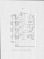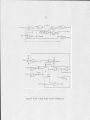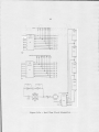
1
Improving an analog computer by adding digital electronics and a digital computer interface by Robert Joseph Horning A thesis submitted in partial fulfillment of the requirements for the degree of MASTER OF SCIENCE in Electrical Engineering Montana State University © Copyright by Robert Joseph Horning (1979) Abstract: The following thesis discusses some possibilities of improving an analog computer by adding digital circuitry and an interface to a digital computer. The thesis work involved modifying an Electronic Associates Inc. TR-48 analog computer and interfacing it to a Digital Equipment Corporation PDP11/03 digital computer. Hardware built as part of the thesis includes circuitry to detect when one of the amplifiers in the analog computer is about to go out of range, circuitry which gives the digital computer the ability to input the output voltage of any amplifier, and circuitry that allows the digital computer' to stop and start the analog computer. A real time clock was also built and added to the digital computer as part of the thesis work. All of the hardware implemented is described in detail in the thesis. The thesis also describes an example problem that demonstrates the capabilities of the implemented system. The example problem shows that an analog computer can be greatly improved by adding digital circuitry and a digital computer interface. The thesis discusses some additional hardware that could be added to the system. It is concluded that giving the digital computer complete control of the analog computer would be unfeasible except for special purpose systems because of the tremendous amount of software that would have to be written on the digital computer. STATEMENT OF PERMISSION TO COPY In presenting this thesis in partial fulfillment of the requirements for an advanced' degree at Montana State'University, I agree that the Library shall make it freely available for inspection. I further agree that permission for extensive copying of this thesis for scholarly purposes may be granted by my major professor, or, in his absence, by the Director of Libraries. It is understood that any copying or publication of this thesis for financial gain shall not be allowed without my written permission. IMPROVING AN ANALOG COMPUTER BY ADDING DIGITAL ELECTRONICS • AND A DIGITAL COMPUTER INTERFACE • by ROBERT JOSEPH HORNING A thesis submitted in partial fulfillment of the requirements for the degree of MASTER OF SCIENCE ' in Electrical Engineering Approved: Head, Major Department ___ Graduate lCJean MONTANA STATE UNIVERSITY Bozeman, Montana June, 1979 TABLE OF CONTENTS THE IMPLEMENTED SYSTEM ............................ 2.1 Introduction ..................... .. 2.2. The Analog C o m p u t e r ................ .......... 2.3 The Digital C o m p u t e r .................... .. , 2.4 The ADVll-A Analog to Digital Converter . . . . 2.5 The DRVll-16' Bit Parallel B o a r d .................... 2.6 The.Real Time Clock ................. ............ . . 2.7 The Over-Range Test Circuitry...................... 2.8. A Program to Demonstrate the System . ■.............. -P- II CTi CTt CT\ INTRODUCTION ................................... . . 1.1 Introduction ................................. 1.2 A Comparison of the Two Types of Machines . . . 1.3 Advantages of Combining an Analog and a Digital Computer' ................................. .. . VO I M H H Page 12 13 19 .25 III SUGGESTED ADDITIONS TO.THE'SYSTEM 3.1 Introduction .............. 3.2 Suggested Hardware Additions 3.3 Suggested Software Projects . '. . . . . . . . . . . . . . . . . . . . . . . . . ........... 31 31 31 40 IV CONCLUSION ........................... 4.1 A Summary of the T h e s i s ............................. 4.2 Suggested' Future P r o j e c t s ............... ........... 43 43 45 APPENDIX A The A/D Converter Distribution Panel Calibration Program . 47 APPENDIX B Circuit Description and Schematics for the Real Time C l o c k .................................. 52 APPENDIX C Circuit Description and Schematics for Over-Range C i r c u i t r y ................................ .......... 63 APPENDIX D Program Listing for Demonstration 69 REFERENCES Program . , .... 81 iv LIST OF TABLES Page Table 2—1 Real time clock status register bit assignment .......... Table 2-2 Over-range test circuitry status register bit assignment 15 23 V LIST OF FIGURES Page Figure 2-1 System Block Diagram . . . . . . . .................... 7 Figure 2-2 Locations of switches, tabs and jumpers on the real time c l o d s .................. -................... .. 16 Figure 2-3 Setting address to the status register 18 . . . . . . . . . Figure 2-4 Setting the interrupt vector for the status register . . .18 Figure 2-5. Block diagram of over-range detection circuitry ........ 22 .Figure 2-6. 5e_t represented in block diagram form and its analog computer realization ................................. 27 Figure 2-7 e . 7 5 t ........................................ 29 Figure 3-1 16 channel D/A c o n v e r t e r ............................... 34 Figure 3-2 Programable gain amplifier 37 ........................... Figure 3-3 Programable analog switches . .............. 39 Figure B-I Real time clock circuit layout........................... 57 Figure B-2 Real time clock s c h e m a t i c s ............................. 58 Figure C-I Over-range detection circuitry schematics 66 vi ABSTRACT The following thesis discusses some possibilities of improving an analog computer by adding digital circuitry and an interface to a.digi tal computer. The thesis work involved modifying an Electronic Associates Inc. TR-48 analog computer and interfacing it to a Digital Equipment Corporation PDPll/03 digital computer. Hardware built as part of the thesis includes circuitry to detect when one of the ampli fiers in the analog computer is about to go out of range, circuitry which gives the digital computer the ability to input the output voltage of any amplifier, and circuitry that allows the digital computer' to stop and start the analog computer. A real time clock was also built and added to the digital computer as part of the thesis work. All of the hardware implemented is described in detail in the thesis. The thesis also describes an example problem that demonstrates the capa bilities of the implemented system. The example problem shows that an analog computer can be greatly improved by adding digital circuitry and a digital computer interface. The thesis discusses some additional hardware that could be added to the system. It is concluded that giving the digital computer complete control of the analog computer would be unfeasible except for special purpose systems because of the tremendous amount of software that would have to be written on the digital computer. Chapter I INTRODUCTION I.I Introduction The purpose of this thesis is to demonstrate that a small analog computer, when augmented with a small digital microcomputer, can be turned into a much more versatile computer tool. The thesis does not attempt to produce an end product comparable with a modern commercial hybrid computer but shows that our existing analog computer can be considerably enhanced in its capabilities by the addition of a digital computer and interface. The following section gives a brief description of how an analog computer and a digital computer solve differential equations. It also discusses some of the advantages and disadvantages of each procedure. Section 1.3 discusses some of the advantages that might be gained by interfacing an analog computer to a digital computer while still operating primarily in the analog mode. Chapter Two gives a more detailed description of the circuits designed and built and the software actually written. Chapter Three discusses some suggested projects. It includes some designs that were not actually implemented. Chapter Four gives some conclusions that were arrived at as a result of the research. 2 1.2 A Comparison of the Two Types of Machines Analog computers are primarily used to simulate systems that can be described by a set of differential equations. In particular rela tionships the outputs of electrical systems to the inputs can be represented by differential equations. It is possible to adjust the components of a mechanical system so that it may be.represented by the same differential equations as a given electrical system, with all the variables of the mechanical system represented by voltages. The primary component of an analog computer system is the operational amplifier (op amp). With resistive feedback the op amp acts as a . voltage summing amplifier, With capacitive feedback, the output is the integral of the sum of the inputs. The op amp can also be made to differentiate, but differentiators are highly susceptible to noise and thus are seldom used. There are other components that are present in most analog computers, but these will not be discussed here. For more information on the components of an analog computer, see references (I), (2), and (3). The solution to a problem on an analog computer is a voltage, observable on an oscilloscope or a voltmeter, or recorded on an XY plotter. The solution may be real time or it may be scaled in time. For problems with small time constants, time is slowed down by in-' creasing the time constants in the analogous electrical system. For problems with large time constants, time is speeded up by decreasing 3 the time constants in the analogous electrical system. Usually the amplitude must also be scaled in order to stay in the linear range of the op amps. For more information on time and amplitude scaling, see reference (I). The analog computer is controlled manually. The problem is first wired on a patch board (this is where the bulk of the work is in pro graming an analog computer). Next the computer is put in RESET mode and a static check is made, i.e. , the initial conditions are checked for validity. Finally the computer is put in OPERATE mode and the solution is generated. At any time during the run of the program the computer may be put in HOLD mode. In this mode the solution is stopped and conditions can be changed or observed and the problem restarted. When an op amp goes out of its linear range on the analog com puter, an indicator light goes on telling which amplifier is out of range. The problem with this is that the light does not come on until the amplifier has been out of range for a few seconds and thus the problem must be restarted from the beginning. When a digital computer is used to solve differential equations, numerical methods are used to approximate the solution. Methods such 1 as Runge-Kutta and Adams-Molton, when used with a small enough step size, can get very nearly exact solutions to differential equations (4). On the other hand, an analog computer cannot be expected to have more than about one per cent accuracy. 4 A digital computer also has the advantage of having a greater dynamic range. One of the big advantages that a digital computer has over an analog computer is greater ease in programming and debugging the problem. M o d e m hybrid computers have alleviated this problem through the use of FORTRAN type programs that set up the problem through the digital portion and through the implementation of auto patching. There are three main advantages to using an analog computer. first is that once the problem is set up it will run faster. The The second advantage is that the problem.can be set up so that there is a one-to-one correspondence between the different blocks of the system being simulated and the components of the analog computer. Finally, it is not necessary to learn numerical analysis as is necessary to understand a digital algorithm. I.3 Advantages of Combining an Analog and a Digital Computer In recent years prices of digital circuitry and digital computers have dropped to the point where it has become feasible to incorporate digital circuitry and a computer interface into most electrical equip ment of any complexity. A digital computer can be used to control and monitor an analog computer. The outputs can be monitored and results stored so that curve fits can be done on the data later, off-line. The digital com 5 puter can also be used to monitor the op amps to check when they are about to go out of range, and to put the analog computer in HOLD be-1■ fore the solution becomes incorrect because of non-linearity in the op amps. When this occurs the digital computer can indicate the action to be taken by the programmer in order to stop the analog com puter from going out of range or perform the necessary operation if digital control circuits are part of the system. The digital computer can also be used to do an automatic static check and to set up initial conditions on the integrators. If this were done, iterative, problems such as solution of boundary value differential equations using the shooting method could be solved automatically (2, 4). . There are many more ways in which a digital computer might enhance an analog computer, but only the above will be discussed in this thesis. The next chapter will describe the circuits that were actually built and the software that was written. Chapter Three will describe the hardware and software that would have to be implemented in order to obtain all the capabilities mentioned above. Chapter II THE IMPLEMENTED SYSTEM 2.1 Introduction This chapter gives the description of all the designs that were actually implemented as part of the thesis project. It first gives a brief description of the two computers that were used in the project. These are the Electronic Associates Inc. TR-48 Analog Computer and the Digital Equipment Corporation’s PDPII/03. added to the two computers is discussed. Next, the hardware that was This includes two boards that were purchased for the PDPII/03 and one that was designed, and built by the author. The two boards purchased were an analog-to-digital con verter and a 16 bit parallel I/O board. programable real-time clock. The custom board was a Equipment added to the TR-48 analog com puter includes an interface to the digital computer and circuitry to place the analog computer in the HOLD mode and then signal the digital computer to take action when an amplifier is about to go out of range. In the final section of this chapter software that was written to demonstrate the use of the system is described. A block diagram showing how the different parts of the system are interconnected is shown in Figure 2-1. 2.2 The Analog Computer The TR-48 is. a general purpose analog computer that was built in the early 1960’s. The TR-48 has forty-eight op amps of which fourteen 7 interfaced Real Time directly to bus Clock PDP11/03 Digital Computer clock overflow start conversion line interfaced directly to bus Converter one analog line analog lines control lines TR-A8 Analog Computer amplifier outputs over-range check circuitry operate/halt control line Figure 2-1 : System Block Diagram interrupt request line 8 may be used' as integrators. Xt also has a number' of other functional blocks such as comparators, multipliers and diode function generators, but these have ho significant effect on the designs presented in this thesis. The linear range of the op amps is from minus ten volts to plus ten volts. There are six modes of operation on the TR-48 analog computer. (1) The POTSET mode is used to set up the problem by applying ten volts across the potentiometers so that they can be set to the desired values'. (2) The SLAVE mode is used when it is desired to run two TR-48 computers in parallel. (3) The REP-OP mode, or repetitive operation mode, is used when it is desired to display the solution to a system with a small, time constant on an oscilloscope. . The problem will be restarted at a predetermined rate. With the introduction of a good storage oscilloscope this mode is not as essential as it once was. (4) The RESET mode causes the intial conditions to be loaded into the integrators. It is used to make static checks and to start a problem. (5) In the OPERATE mode the problem is being run. Normally, the programmer'.will put the computer in RESET mode and then OPERATE mode. (6) HOLD mode suspends the solution. All the op amps will hold their values when the HOLD mode is entered. The designs in this thesis will give the digital computer and 9 digital circuitry control of the OPERATE, RESET, and HOLD modes. 2.3 The Digital Computer The PDPlI/03 is a 16 bit microcomputer system with 28K words of memory and a dual floppy disk. It has extensive software including a monitor, an editor for building files, file handling programs, a FORTRAN compiler and a macro-assembler. devices as memory locations. boards to the system. 28K to 32K. The PDPl1/03 treats all input-output This makes it quite easy to add new Input-output modules occupy the addresses from Daisy-chained grant signals provide a priority-structured interrupt I/O system.(5)/. Priority is determined by the physical loca tion of devices on the backplane. When an I/O device's interrupt re quest is granted, the device sends to the processor a vector address that points to the location in memory of the interrupt servicing routine, thus eliminating the need for device polling on the occurrence of an interrupt. The PDP11/03 uses a software stack to store return addresses for. interrupt routines and subroutine calls. This makes it quite simple to write transparent interrupt routines and subroutines which will automatically sequence correctly. 2.4 The ADVll-A Analog to Digital Converter In order to monitor the solution to a problem on the analog compu ter, the digital computer must be provided with an analog to digital (A to D) converter. It was decided that the ADVll-A A to D converter 10 built by Digital Equipment Corporation was adequate for the job.. The ADVll-A is a 12 bit converter and uses a successive approximation tech nique to make the conversion. It multiplexes sixteen single ended or eight quasi-differential analog channels. The A to D converter can operate in single ended mode or quasi-differential mode. (It is not true differential in that it does the A to D conversion on one line and then does the A to D conversion on the other line and takes the difference.) The single ended mode was selected because the computers are in close proximity to one another so that the noise picked up in the cable would be negligible compared to the noise picked up in the patch board. (The currents in the cable are very small compared to the currents in the. patch wires.) The analog input range is between -5.12 volts and +5.12 volts. The ADVll-A takes up two address locations on the PDP11/Q3 bus. One location is a buffer that holds the results of the conversion. The other location is a 16 bit status register which is used to control the converter and to monitor its status. status register see reference (6). For a complete description of the Only the features of the status register used in the designs for this thesis are discussed below. A to D Start - This is a bit that is set by program control and causes the ADVll-A to start a conversion. External Start Enable - This bit is set by program control and allows an external signal to cause a conversion to start. The external signal must be provided to a tab on the ADVll-A board and conversion 11 starts on a high to low transition of this signal. A to D Done - This bit is set by the ADVll-A when a conversion is done and the result is ready in the buffer. When the buffer is read the A to D Done bit is automatically cleared. Done Interrupt Enable - This bit is set by program control and causes the ADVll-A to generate an interrupt request when a conversion is done, i.e., when A to D Done is set. Multiplexer Address - This is a set of four bits set by program control that give the channel address on which the conversion is to be made. A to D Error - This bit is set by the ADVll-A for one of three reasons. It is set if an external start is attempted before the chan nel multiplexer has had time to settle. It is set if an attempt is made to start a conversion when a conversion is in progress. Finally, it is set by failing to read the results of a previous conversion be fore the end of the current conversion. Error Interrupt Enable - This bit is set by program control and causes the ADVll-A to generate an interrupt request when the A to D Error bit has been set. When using the ADVl1-A, the programmer must be careful not to start a conversion for nine microseconds after the channel multiplexer address has been set. The multiplexer must be given, this amount of time to settle. The conversion time of the ADVll-A is thirty-two microseconds. 12 When interrupt I/O is used, a through-put rate of about 32 KHz is obtained if all the conversions are made on one channel. If the input channel is changed between every conversion, nine microseconds must be added to the conversion time thus dropping the through-put rate to about 25 KHz. It was necessary to build a distribution panel for the A to D converter. Because the ADVll-A has an input range from -5.12 t o +5.12 and the TR-48 analog computer has a range from -10 to +10 volts, it is desirable that some of the channels on the A to D converter have divide by two voltage dividers. This was done to the top five channels (10-15) by inserting 10 K-Ohm voltage dividers. On these channels this lowers the input impedence to the A to D converter to 10 K-Ohm. This is acceptable because of the low output impedence of the op amps on the analog computer. However, caution should be taken if the distribution panel is used elsewhere. The problem could be corrected by adding op amp buffers to the inputs of these channels. Appendix A contains the listing of a program that will assist the user in calibrating the voltage dividers on the distribution panel, along with directions on how to use the program. For more information on the ADVll-A board and information on how to program it, see reference (6). 2.5 The DRVll 16 Bit Parallel Board In order to communicate with the digital circuitry that was added to the analog computer, a DRVll 16 bit parallel input-output board was 13 purchased from Digital Equipment Corporation. for output. The DRVll was used.only Therefore, the input channel could be used for some other purpose. The DRVll has an output buffer, an input buffer, and a status regis ter. The status register has two request flags that can be set by the circuitry with which the computer is communicating. interrupt enable bit for each of these flags. It also has an When the interrupt enable bit is set and the corresponding request flag is set, the DRVll will generate an interrupt request. Lastly, the DRVll status register has two flags which are set and cleared under program control. How the output buffer register was used to control the digital circuitry will be described in Section 2.7. For a more detailed description of the DRVll board, see reference (6). 2.6 The Real Time Clock In order to do data acquisition or real time control using a digital computer, it is necessary to have samples accurately spaced. there was a need for a programable real time clock. Thus A clock could have been purchased from Digital Equipment Corporation, but the only one available had more features than were necessary and also took two slots on the PDP11/03 backplane where a custom board would take only one slot. It was also decided that the real time clock would be more economical to build than to buy. Since this board was built as part of this 14 thesis, a detailed description of its use is given'here. Appendix B has a detailed description of how the board is put together along with schematics for the board. The real time-clock has a buffer register and a status register. The buffer register is loaded with a negative number (in two’s complement form). When the clock is enabled the buffer is counters. The counting frequency is status register. loaded into a set of determined by three bits of the When the counter overflows, the overflow flag of the status' register is set, a pulse is given on an external connector tab (this can be used to start the A to D converter), and.the buffer is loaded into the counters again. If the interrupt enable bit is set in the status register, the real time clock will generate an interrupt request. If the overflow flag of the status register is not cleared by the time that a second overflow occurs, an error flag is set. summarizes how the bits of the status register are used. Table.2-1 (The bits are numbered 0 to 15, from right to left.) The time base for the real time which, when divided by two, produces clock is a 2 MHz crystaloscillator the needed I MHz signal. The I MHz signal is divided by ten four times to give the other needed frequencies. When an external frequency is to be used with the counter, the sig nal should be connected to connector tab A. location of connector tab A.:) (See Figure 2-2 for the The external input is TTL-compatible and consists of one TTL unit load. When an overflow occurs a pulse will be generated on connector tab B 15 Table 2-1 Real time clock status register bit assignment Bit 0 Clock Enable - set or cleared under program control and causes the buffer to be loaded into the counter and counting to start. Bits 3, 4, 5 Counting Frequency - determines the rate at which the counter counts. 000 001 010 011 100 101 HO 111 - does not count I MHz 100 KHz 10 KHz I KHz 100 Hz external Line (60 Hz) Bit 6 Interrupt Enable - set by program control and causes the real time clock to request an interrupt when an overflow occurs. Bit 7 Overflow Flag - set by real time clock when an overflow occurs and cleared by program control. Bit 12 Error Flag - set by real time clock when an overflow occurs while bit 7 is still set. Cleared when bit 7 is cleared. — — ----- --- ---- 16 Tab B Tab A power jumpers O O Figure 2-2 : Locations of switches, tabs and jumpers on the real time clock. 17 (See Figure 2-2 for the location of connector tab B.) This external out put is TTL-compatible and capable of driving about eight TTL unit loads. (The External Start on the analog-to-digital converter presents five TTL unit loads. It is assumed'that connector tab A will be connected to the External Start connector tab on the A to D converter.) The address of the. status register is determined by the settings of the DIP switches 7 and 8 on SWl, and I through 7 of SW2., (See Figure 2-2 for the locations of SWl and SW2.) The address of the buffer register is the address of the status register plus two. - It is two greater than , . the address register is because the PDPlI/03 has byte (8 bits), addressing and thus 16 bit words have even numbered addresses. how the address is determined. (8K bytes) of memory. Figure 2-3 shows Notice, that the address is in the top 4K Digital Equipment Corporation recommends that the . real time clock address be set to the octal address 170420. The interrupt vector is determined by the settings of switches I through 5 of SW2. mined. Figure 2-4 shows how the interrupt vector is deter The interrupt vector points to an address in memory that contains the address of the. interrupt service routine. The program counter will be loaded with the address of the interrupt service routine when an inter rupt is granted to the real time clock. The address following the new program counter address contains the new status word. counter and status word are pushed onto the stack. The old program Only the bottom byte of the vector address can be set by the switches and thus the location of the interrupt vector must be in the bottom 128 words of memory. (The 18 Switch on Switch off 0 I Figure 2-3 : Setting address to the status register. S5 S4 S3 S2 SI SWl Switch on Switch off 0 I Figure 2-4 : Setting the interrupt vector for the status register. 19 PDPl1/03 operating system leaves the lower part of memory for interrupt, vectors.) It is recommended that the vector address for the"real time . clock be set to octal 370 (byte address) because this address is not used by any existing devices. The five volt power supply on the PDPII/03 was loaded to its limit, it thus became necessary to use an extra five volt power supply. The extra power supply was connected to the first four slots following the • CPU board on pin AUl . this pin.) (See reference (7), page 303, for location of The reason the top four slots were used is that these have the highest priority and the real time clock should have a high priority since time is critical for good results. If it is desired to use the regular power supply to power the real time clock, the jumper should be removed from module pin AUl and installed between jumpers I and 2. For. the locations of jumpers I and 2, see Figure 2-2. 2.7 The Over-Range Test Circuitry One of the main problems with an analog computer is that the op amps go out of linear range. This problem is exacerbated because it is difficult to tell exactly when an amplifier goes out of range. Conse quently, when the solution to a problem goes out of range the programmer must rescale the problem and start over from the beginning. To allevi ate this problem, circuitry was added to the analog computer to sense ■ when any amplifier was about to go out of range. When an amplifier approaches an out of range condition the analog computer is automatical- 20 Iy put in HOLD mode and the digital computer is signalled to take ac tion. It is assumed that the digital computer will read the values of a l l ,amplifiers and pass the information on to either the user or an automatic rescaling routine. The schematics for the over-range detec tion circuitry are given in Appendix C, along with a description of the circuitry. A description of how the circuitry operates and how it is programed is given here. It is obvious that multiplexing is necessary in the design because there are only sixteen channels on the A to D converter and forty-eight op amps must be monitored. Also, it is desirable to have as many channels available as is possible for data acquisition. Another con sideration is that the converter can only sample at about 30 KHz, which means that if it were desirable to check each amplifier at a frequency of 500 Hz, the digital computer would have.very little time to do anything else. Three comparators were each multiplexed to sixteen op amps through a set of analog switches. The analog switches were controlled by a 4 to 16 line decoder, which was driven by a 4 bit loadable counter. circuitry can be run in two modes. The In the usual mode the up counter counts at a frequency of a little over 10 KHz. This causes each op amp to be checked for. over-range condition at a rate of about 625 Hz. (The sampling frequency was determined by the slew rate of the op amps driv ing the analog switches used for multiplexing.) If an op amp is about to go out of range the analog computer will be put in HOLD mode auto '21 matically and the digital computer alerted. In the other mode the digital computer will disable the'10 KHz clock and load a value into the counter. This value selects which three ampli fiers are multiplexed into the comparators. The inputs to each of the comparators are also multiplexed through a set of analog switches. These three analog switches are controlled by the digital computer. The outputs of this multiplexer will normally be connected to one of the channels of the A to D converter through a banana plug connector. In summary, this allows the digital computer to obtain the value of the output of any op amp. . A block diagram of, the analog multiplexer is shown in Figure 2-5. The interface of the digital computer from the overload checking circuitry was accomplished by the use of the DRVll 16 bit parallel input/output board described in Section 2.5. The buffer of the parallel board was used as a control status register for the overload checking circuitry. The way this control status register is used is shown in Table 2-2.’ The use of the control status register must be clarified. Using the multiplexer address along with the load bit permits access to the output of any op amp while the problem is running. However, caution must be used when this is done because when the over-range circuitry is in the load mode only the amplifier being observed is being checked for over-range.(the counter is disabled). Normally the load mode is only used when the analog computer is in HOLD mode. 22 Op-Amps 0-15 Analog Comparator Multiplexer Analog Output Analog Multiplexer Op-Amps 16-31 Analog Comparator Multiplexer Op-Amps 32-47 Analog Multiplexer Loadable 16 Bit Counter Comparator' Digital Control ; Circuitry and Computer Interface Figure 2-5 : Block diagram of over-range detection circuitry. 23 Table 2-2 Over-range test circuitry status register bit assignment I Ii Bits 0-5 Multiplexer Address - The bits O through 3 are loaded into the counter when the load bit is set. Bits 4 and 5 are used to multiplex one of the three comparators' inputs to the Analog to Digital Converter. Bit 6 Not used. Bit 7 Load Bit - Set by program control. When set it will disable the 10 KHz clock and load the multiplexer address into the counter. Bit 8 Auto Hold - When set by program control the analog computer is automatically put in HOLD mode. Bits 9-14 Not used. Bit 15 Auto Operate - When set by program control the analog computer will automatically be put in OPERATE mode. 24 The voltage detected by the A/D converter is half the voltage of the op amp being monitored because the A/D converter has a range from -5.12 to +5.12 volts, while the op amps have a range of -10 to +10 volts. Also, the analog switches used can only handle a differential of 15 volts. In the design the analog switches are switched between +6 volts and -6 volts (or a 12 volt differential). When using the over-range detection circuitry to read in voltages the user must be sure to give the multiplexer time to settle. At least 100 microseconds should be allowed. If both the Auto Hold bit and the Auto Operate bit are set the analog computer will stay in HOLD mode. Also, if the Auto Operate bit is set while an op amp is over-range the analog computer will stay in OPERATE mode and the overload circuitry will not generate an interrupt to the digital computer. Normally when the Auto Operate bit is used to start the solution it will be set and immediately cleared. It was decided that the Auto Operate bit would have priority over the over range circuitry so that the user could by-pass the over-range circuitry if he desired. There is also a manually operated switch on the front panel of the over-range circuitry which will give control of the analog computer back to the user. This switch is located on the front of the case of the over-range detection circuitry. The over-range detection circuitry provides a link between the analog computer and the digital computer. This interface can be used in any way desired but was meant to be used in the following way. 25 The digital computer uses the console terminal to instruct the operator to put the analog computer in RESET mode. Next, the digital computer sets bit 8 of the control status register (the Auto-Hold bit). This does not affect the mode of the analog computer because the HOLD mode is accomplished by disabling the OPERATE mode and thus AutoHold only has effect when the analog computer is in OPERATE mode. Next, the operator is instructed to put the analog computer in OPERATE mode and to signal the digital computer that this has been done (by use of the console terminal)., The digital computer will then clear the AutoHold bit and pulse the Auto-Operate bit. This will start the solution. If an op amp goes over-range the analog computer is put in HOLD mode by disabling the OPERATE mode relay, and the digital computer receives an interrupt. The interrupt routine will store all the voltage values of the op amps and instruct the operator to take action. 2.8 A Program to Demonstrate the System The previous sections of this chapter described all the hardware that was constructed as part of this thesis. This section will summa rize the system that is now available and describe the program that was written to demonstrate how the system can be used. A listing of the program is given in Appendix D. Basically what exists is an analog computer being monitored and partially controlled by a digital computer. system is shown in Figure 2-1. 'A block diagram of the The digital computer is capable of 26 acquiring data from the analog'computer' and deciding if the'solution should be stopped. Data can be stored on disk to be evaluated after the solution has been run. The solution will be stopped if an op amp attempts to go out of range. is alerted to take action. When this happens, the digital computer The digital computer can read in the values of all the amplifiers, store them on disk, and alert the operator to correct the problem. The solution need not be started over because the stored values can be used as initial conditions when the problem is re scaled. However, it must be remembered to also rescale the initial conditions. ■' The program that was written uses all the capabilities mentioned above. It does not solve a practical problem on the analog computer, but it does demonstrate how the equipment is used. . The program only uses a few op amps of the analog computer. simple functions are realized. Two They are a declining exponential and a rising exponential. The declining exponential has a time constant of one second and initial condition of five volts. The block diagram (as used in feed back control theory) for the function and the analog computer wiring diagram are shown in Figure 2-6. See reference (8) for more informa tion on feedback control theory, and reference (I) for information on the symbols used in analog computer wiring diagrams. The rising exponential was given a time constant of .75 seconds and an initial condition was chosen to be one volt. These values were 27 5(l-u(t)) a) ^ A/D Channel 15 block diagram form -1 0 O — channel 15 b) analog computer wiring diagram Figure 2-6 : '5e-t represented in block diagram form and its analog computer realization. 28 chosen so that the integrator would go out of range after about three seconds. The block diagram and the analog computer wiring diagram are given in Figure 2-7. Notice that the A/D converter output had to be taken off a separate op amp buffer from the actual output. This is be cause of the relatively low input impedences of channels 11 through 15 (the divide by two channels). why this is so. See Section 2.4 for the explanation of When channels put in parallel with or hooked 11 through 15 are used they must not be to the output of one of the analog computer potentiometers. After the problem was set up on the analog computer, the program on the digital computer was run. This program first asks the operator 0 for the name of the two disk files in which the data from channels 14 and 15 are to be stored and the name of the file in which the outputs of the amplifiers are to be stored if there is an over-range interrupt. The operator is then instructed through the console terminal to put the analog computer in RESET mode, let it settle and then put it in OPERATE mode. When a linefeed character is input on the console the solution is started. The digital computer samples each output every .0.3 seconds. samples are stored and checked to see if they are over When one is over eight volts, the solution is stopped, The eight volts. i.e., the analog computer is put in HOLD mode, and the operator is. asked if the solution should be continued. If the response is positive the analog computer is put in OPERATE mode and the solution is continued. 29 unit impulse a) channel 14 block diagram form channel 14 b) analog computer wiring diagram Figure 2-7 : e .75t 30 When an op amp goes out of range because of the rising exponen tial, the solution is stopped, the values of all the op amps are stored, and a message is set to the console. At this point exponential curve fits were done on the input data. The fits showed the input data to match the modeled exponentials quite well. value. The highest error was within one half per cent of the expected Chapter ,III SUGGESTED ADDITIONS TO THE SYSTEM 3.1 Introduction The system as it now exists can digitally monitor the solution and automatically stop or start the solution. What the system lacks in hardware is the capability of using the digital computer to affect the solution on a real time basis, and the capability of digitally restart ing the problem with ,new initial conditions that were determined and set by the digital computer. Section 3.2 will discuss hardware! that can be implemented to give the system the capabilities mentioned above. In order to completely exploit the system,, a large amount .of soft ware must be written. Section 3.3 will discuss some software goals that if met, would give much of the work now done by the user to the digital computer. 3.2 Suggested Hardware Additions The hardware needed to complete the system as discussed in the introduction of this chapter would probably cost about the same for components and be about the same size as the hardware discussed in Chapter II. The most desirable piece of hardware that could be added to the system would be a digital to analog (D/A) converter. The D/A converter would give the system the capability of automatically setting the initial conditions of the integrators and the capability of enabling 32 the digital computer to change inputs to the problem as the solution progressed. The D/A converter should have at the very least sixteen channels. This would give fourteen channels to set the initial conditions in each of the integrators and leave two channels- to use as real time inputs to the solution. The D/A converter would preferably have twelve bits of resolution in order to match the resolution of the analog to digital converter. The speed of the D/A converter should be faster than thirty- microseconds (the speed of the A/D converter). The range of the convert er should be between -10 and +10 volts to match the range of the analog computer.Digital Equipment Corporation has available a D/A converter built for the PDPII/03 that meets all the requirements except that it has only four channels. One of these channels could be multiplexed into sixteen sample and hold circuits to meet the requirement of having at least sixteen channels. However, with just a little more effort and a lot less expense, a 16 bit parallel board can be used to give the digital computer control of circuitry that contains the multiplexing and the sample and holds along with a D/A converter. A D/A converter chip that meets all the specifications can be purchased for under twenty dollars (10). The output of the D/A converter would be multiplexed to the inputs of the sample and hold circuits in much the same way that the analog computer op amp outputs were multi plexed to the A/D converter. However, it should not be necessary to 33 multiplex the actual analog signal as will be shown in the suggested design. Sample and hold chips could be purchased or the sample and holds could be realized with op amps and analog switches. Reference (9) gives some examples of sample and hold circuits realized with op amps and analog switches. With only sixteen bits to work with on the status register (the output buffer of the parallel board), it is necessary to share some bits. This is because twelve bits are needed for the data input to the D/A converter and four bits for the multiplexer. control. This leaves none for The data bits for the D/A and the multiplexer address bits could be shared* This leaves four bits for control. One could be used to load the buffer for the D/A, one could load the multiplexer address, one could enable the multiplexer, and one would be left as a spare. A suggested design is shown in Figure 3-1. Bits 0 through 4 are shared by both the D/A buffer and the multiplexer address buffer. The remaining bits of the D/A buffer occupy the positions from 5 to 11. Bit 12 is used to load the multiplexer address buffer, bit 13 enables the multiplexer, and bit 14 loads the A/D input buffer. Notice that all the inputs of the sample and holds are tied to gether and thus.no analog signal multiplexing is necessary. Some buffering might be needed on the multiplexer output if the sample inputs on the sample and hold circuits are not TTL compatible. The D/A input buffer could be eliminated by requiring that the multiplexer buffer' be loaded first and the D/A converter allowed' to • ' 34 bits 0-4 Bit Bit Bit Bit Bit Bit Bit Bit Bit Bit Bit Bit Bit Figure 3-1 : 16 channel D/A converter 35 settle before the multiplexer enable bit was set. However, this would lead to programing inefficiencies and is not recommended. The number of D/A channels could be easily increased simply by adding more sample and holds and making the multiplexer larger. With the ability to set the initial conditions on the analog com puter using the digital computer, it becomes desirable to have the ability to put the analog computer in RESET mode using the digital computer. This would give the digital computer the capability of load ing the initial conditions and then starting the problem. Giving the digital computer control of the RESET mode is quite easy. The same type of circuitry that allowed it to control the OPERATE, mode can be used. (See Appendix C.) It is recommended that the control of the RESET mode be given a bit in the status register of the over range detection circuitry. This is because the OPERATE mode control and HOLD mode control bits are in this register and all the mode control bits should be in the same place. It would probably be desirable to build circuitry to prevent a programmer from inadvertently putting the analog computer in both OPERATE mode and RESET mode simultaneously. This can be done by AMDing the Auto-Reset bit with the complement of OPERATE signal to form the effective Auto-Reset signal. It must be remembered that the analog com puter can be in OPERATE mode even if the Auto-Operate bit is not set. The correct signal to use for the ANDing is pin 5 of the 7575 chip shown in the schematics of Appendix C. 36 For the system described to this point, the digital computer com pletely controls:the operation of the analog computer and can change initial conditions and inputs. However, the digital computer cannot automatically change the dynamics of the problem. If, for example, in a particular problem it is known that one of the amplifiers will even tually go out of range, it would be desirable to be able to rescale that particular amplifier automatically. In other words, it would be useful to have some programmable gain amplifiers. The programabIe amplifiers should meet all the specifications of the regular amplifiers (11) except that the gain would be controlled by the computer' rather than by resistors. A suggested method of achieving a programable gain amplifier using an op amp and a set of analog switches is shown in Figure 3-2. •This amplifier resembles a standard D/A converter. The op amp acts as a summer and the transfer function can be expressed as Vout ---Vin =— (b0 + 2bi + 4b2 ... + 2nbn) rI where the b Ts are binary digits (I or 0). The above equation shows that the gain of the amplifier is directly proportional to the binary weighted sum of a set of binary digits or, in other words, a binary number. maximum gain is vOUt Vto™ The values of and /max ^ ( 2 “+1 - I). determine the value of the maximum gain. The programably loaded register W V v.-.. vXyv— ■ O O O 2i 2n V W ---- Figure 3-2 : Programable gain amplifier v out 38 In the actual realization of the programable amplifier of Figure 3-1, it would be desirable to have the outputs of the analog switches buffered. This is because the internal resistance of the analog switches could make the selection of the resistor values difficult or impossible. Doing this would also raise the input impedence of the programable amplifier. If quad op amp chips were used (such as LM325’s), very few chips would be added to the circuit. Eight bits of resolution would meet the requirements for most problems. If this were the case each amplifier would require an 8 bit buffer, two quad analog switch chips, two quad op amp chips, nine precision resistors, and an op amp for the summer. It might also be necessary to buffer the outputs of the buffer to drive the controls of the analog switches properly. A sixteen bit parallel board could be used to load the buffer register. With multiplexing, the same parallel board could be used to load the buffers of any number of programable gain amplifiers. The system could also be reconfigured by the digital computer by the use of'programable analog switches. This would be rather simple and they could be programed' using the'same parallel board that would control the programable gain amplifiers. The outputs would have to be buffered in order to eliminate the effects of the resistance in the analog switches. Figure 3-3 shows a suggested design for the program controlled analog switches. If the system were configured with all of the components discussed control buffer Figure 3-3 : Programable analog switches. 40 to this point, a.very.versatile- hybrid machine would.be obtained. ever, one essential.element is missing from the system. is the’software. How That.element The'next.section will discuss some software that could, be. written to take advantage of the system. 3.3 'Suggested'Software Projects The development of the software necessary to fully exploit the hardware.developed in this thesis would be an immense job. However, just as the hardware was.only developed partially and still resulted in a useful system, the software could be partially developed and still be useful. This,section suggests some software projects that might be undertaken in order to enhance .the system. One of the main tasks of the digital computer is that of data acquisition. This task must be.performed in a real time mode and thus very little should.be done as far as data.reduction (such as converting the voltages to the simulated variables) while data is being acquired. However, if a large amount of data is being input (on.the order of 100,000 samples or more) it might be desirable to compress the data. Since.the data has twelve bits of.resolution a n d .the w o r d .length of the computer is sixteen bits, it is possible to store four words of data.in three computer words. This.increases the problem of programing but saves twenty-five per.cent.in storage space. Another problem that must not be overlooked is .that of what to do when .the solution is .rescaled. When .the solution is.restarted it must be remembered that the new data 41 is to be multiplied by a different scale factor. When'it becomes necessary to rescale the problem it would be pos sible to have a software routine that would do the rescaling. If the rescaling involved a programable gain amplifier the routine could reset the gain of the amplifier and restart the program. If it in volved one of the analog computer op amps, it could notify the operator to reset the gain or gains. It would be desirable to have this routine keep track of how the acquired data must be scaled and to pass this information on to a data reduction routine. The data reduction routines would usually be run after the comple tion of the problem and would normally be written in FORTRAN. (The real time routine might be written in assembly language because of speed consideration). Programing in FORTRAN has the advantage of being easier to program and ^provides..'access, td canned programs. The data reduction routines would do things like convert the data to the proper units, plot the'data and do curve fits on the data. A type of problem that has been briefly mentioned but not expounded upon is the iterative type problem. soft. Boundary value problems are of this In this type of problem some of the initial conditions are known and some of the end conditions are known. tions are guessed and the solution run. The unknown initial condi The computed end conditions are compared' to the known end conditions and this information is used to estimate new initial conditions. some tolerance is met. This procedure continues until It would be desirable to have a real time 42 routine to load the initial conditions using the D/A converter and to reset the analog computer, and then restart the problem. This same rou tine would acquire the end conditions and pass them to a file. A second routine (probably written in FORTRAN) could read the file and calculate the new estimated initial conditions and pass this information to a second file. The original routine could be restarted. It would read in the new initial conditions, load them into the analog computer, and start another iteration. ance was met. This would continue until the required toler The FORTRAN routine would also check to see that the solution is remaining stable. The most difficult software problems would be ones which would reconfigure the system. However, there are particular problems that could take advantage of this capability without too much effort. example is the simulation of a system that varies with time. An The hybrid system could be used to develop an adaptive controller for such a system. One of the main goals in developing software for a system of this type should be to make it general purpose and easy to use. Any soft ware developed for the system should be developed with the idea of making the system easier to program. ■ Chapter IV - ?•< CONCLUSION 4.I A Summary of the Thesis This thesis illustrates' that an analog computer can be made a more useful tool through the implementation of digital circuitry and an interface to a digital computer. The hardware built gave the digital computer the capability of monitoring the analog computer for over-range conditions (or some other condition) and acquiring data. The digital computer could stop and start the solution but had no capability of actually entering into the problem solution. The program in Appendix D demonstrates all the capa bilities of the hardware. This program can be used to acquire data and monitor for over-range conditions for any problem run on the TR-48 analog computer with little or no modification. Some modifications would be required if data were to be acquired from more than two ampli fiers. The program is documented quite extensively. Therefore, .modi fications, should not be.a great problem. The digital computer can start and stop the solution but has no capability of actually entering into the problem solution. tation makes the hardware relatively easy to use. This limi The hardware described in Chapter III would give the digital computer the ability to interact in and reconfigure the problem. The hardware could be built without great expense, i .e., it could be realized with standard TTL and linear components. However, the software requirements for the system 44 would be extensive. For the noninteractive system the software only checked'for'some condition and stopped'the solution when this condition was met. In an interactive system the software must choose among a number of alternatives'. 1) Some of the possibilities are listed below. The problem may have to be rescaled. An amplifier about to go out of range would be adjusted to prevent it from going out of range. Data being acquired must also be rescaled. The condition of an ampli fier output being scaled too low must also be checked. The error of the amplifiers is a percentage of full scale so small outputs have the larger per cent error. 2) If may be necessary to calculate new initial conditions and restart the problem. This would be necessary in boundary value prob^ Iems in which the shooting method was used. 3) It may be necessary to change the gains of various blocks in the problem being solved. The software may have to rescale in both amplitude and time when this is done. An example of this would be in the simulation of adaptive control systems. 4) The problem may be reconfigured by the use of analog switches. This might be necessary in the simulation of nonlinear (relay type) problems. 5) Lastly, it may be necessary to stop the solution and store the end conditions. This might be done because the solution is finished or has gone unstable. The tasks listed above are only a' part of the software problem. 45 The digitally set inputs must be controlled. quired and stored. Data must still be ac Also, it would be highly desirable to have soft ware to help set up the problem. This is especially true with the digitally controlled components of the system. In conclusion, it appears that the major obstacle to overcome in completely hybridizing an analog computer is the software problem. The software is a large enough problem to make the complete hybridization of an analog computer unfeasible. It is shown, however, that an analog computer can be improved through the use of a digital computer and.digital circuitry. ■ Particular, advantages'were readily apparent in output data collection and presenta tion. The ability to prevent the problem from going over-range and the ability to acquire data in digital form were added to the system without undue expense and without the heed to develop extensive soft ware. Finally, although a PDPII/03 microcomputer is used in this system, a much smaller and more compact system could be realized using a micro computer such as the Billings Microsystem System which employs a Z80A microprocessor, display, floppy disks, and input/output processor all in a single terminal. 4.2 Suggested Future Projects This section gives some ideas on improving the system without completely hybridizing it. 46 Although the sample program is easy to adapt to any problem it would be desirable to have a program that required no manipulations to work on any problem (to the limits of the hardware). Such a program would have inputs such as number of A/D channels needed, sampling rates for A/D channels used, how long to run the problem, and on what condition to stop the problem. It would be desirable to have a program that converted the data from the binary representation used by .the A/D converter to the actual units of the system being simulated. This program would have for inputs scaling factors and the output files from a solution run. It. would also be desirable for this program to have plotting capabilities. Although it would most likely be unfeasible to implement the complete hybrid system suggested in Chapter III, it might be useful to use some of the hardware suggested to implement a special purpose system. For example, if a complex' system (one using a large percentage of the analog computer components) was being simulated and it was desired to develop a digital controller for the system, it would be desirable to have a D/A converter. The additional software required would only involve software to realize the controller. APPENDIX A 48 The A/D Converter Distribution Panel Calibration Program In order to' run this calibration program jumper together channels 10 through 15 of the distribution panel. Next, apply about five volts to these jumpered channels and run the program. The name of the Load Module is PNLTS.SAV. The program will compare channels 11 through 15 to channel 10 and instruct the user which way to turn the pots on the distribution panel. The number given for each channel by the program can be used to esti mate how many times the particular pot should be turned. Divide this number by two to get the estimate. The program should be run until all numbers output are less than or equal to one. Tb leave the program, hit control "0". 49 >THE FOLLOWING PROGRAM IS USED TO CALIBRATE THE CHANNELS 511 THROUGH 15 ARE DIVIDED BY TWO CHANNELS AND 5EACH HAS A POT THAT IS USED TO CALIBRATE THE 5CHANNEL. 5 5TO USE THIS PROGRAM APPLY FIVE VOLTS 5TO CHANNELS IO THROUGH 15. THE PROGRAM 5READS THE VALUE OF THE VOLTAGE AT EACH 5OF THESE CHANNELS AND CALCULATES HOW EACH POT 5MUST BE TURNED IN ORDER TO MAKE THE VOLTAGES 5AT CHANNELS 11 THROUGH 15 EQUAL TO HALF THE 5VOLTAGE AT CHANNEL 10. 5RUN THE PROGRAM UNTIL ALL VALUES OUTPUT TO THE 5PRINTER ARE EQUAL TO I OR 0. 5 5TO GET BACK TO THE MONITOR HIT CONTROL C, y A/D CONVERTER DISTRIBUTION PANEL, R0=%0 Rl=Zil R2=%2 R3=%3 R4 = %4 R5=%5 R6=%6 R7=%7 ,MCALL .PRINT,♦TTYIN,..V2.,,.TTYOUT ..V2., START: CLR 0*402 LOOPl: .PRINT *MSG .TTYIN ♦PRINT *HEAD ♦TTYOUT Il=SPACE MOV * INTRI,0*400 MOV *5100,0*170400 INC 0*170400 WAIT 5OUTPUT MSG AND WAIT 5FOR A LINEFEED TO BE 5INPUT 5PRINT THE HEADING 5SET THE A/D VECTOR 5SET A/D STATUS REG. 5START CONVERSION 5WAIT FOR INTERRUPT 50 MOV *INTR2,e*400 LQ0P2J INCB @4170401 TSTB @4170401 BEQ LOOPl INC @4170400 WAIT BR L00P2 ?CHANGE A/D VECTOR fCHANGE A/D CHANNEL 5ALL CHANNELS TESTED? ;RESTART IF DONE ?START CONVERSION $WAIT FOR INTERRUPT rCHECK NEXT CHANNEL INTERRUPT ROUTINE TO READ IN VOLTAGE ON CHANNEL 10 INTRl: MOV 170402,Rl ADD 44000,Rl RTI JRl GETS A/D INPUT JADD 4000 TO Rl JRETURN TO PROGRAM JINTERRUPT ROUTINE TO CHECK CHANNELS 11-15 JAND OUTPUT CALIBRATING INSTRUCTIONS J JR2 GETS A/D INPUT INTR2J MOV 170402,R2 JLOAD 4 INTO R4 MOV 44,R4 JMULTIPLY R2 BY 2 ASL R2 JSUBTRACT Rl FROM R2 SUB R I ,R2 JBRANCH IF POSITIVE BGT GRTH JNEGATE R2 NEG R2 JPRINT THE WORD RIGHT .PRINT 4RIGHT .TTYOUT 4SPACE JTO THE PRINTER JBRANCH TO RETRN BR RETRN JPRINT THE WORD LEFT GRTHi .PRINT 4LEFT JON THE PRINTER .TTYOUT 4SPACE JROTATE R2 FOUR RETRN: ROL R2 JTIMES IN ORDER ROL R2 JTO SET IT UP TO BE ROL R2 JOUTPUT AS ASCII ROL R2 JCHARACTERS l o o p s ; r o l R2 J ROL R2 ROL R2 J ROL R2 JMOVE R2 TO R3 MOV R2,R3 JROTATE R2 ROR R2 51 $ CHANGE R3 TO ASCII BICB *370,R3 i CHARACTER BISB *60,R3 ?OUTPUT CHARACTER ♦TTYOUT R3 ;DECREMENT R4 DEC R4 ;IF DONE RETURN BEG RTRN ;BRANCH TO LOOPS BR LOOPS ;OUTPUT A SPACE RTRN ♦ .TTYOUT !SPACE i RETURN TO PROGRAM RTI M S G : .BYTE 15,12 .ASCIZ /HIT THE LINEFEED KEY TO START TEST/ .EVEN CHANNEL 11 CHANNEL 12 CHANNEL/ h e a d : .ASCII / .ASCIZ / 13 CHANNEL 14 CHANNEL 15/ .EVEN LEFT / LEFT: .ASCII / .BYTE 200 .EVEN RIGHT: .ASCII / RIGHT / .BYTE 200 .EVEN s p a c e : .ASCII / / .EVEN ♦END START APPENDIX B 53 Circuit Description and Schematics for the Real Time Clock This appendix describes how the PDPII/03 uses the bus signals to control the real time clock. See Section 2.6 for information on how to use the real time clock. In the schematics all inputs that start with a B and end with an L are inputs from the PDPl1/03 bus. All other labeled inputs can be found as outputs somewhere in the schematics. Figure B-I shows the layout of the board. to identify it. through B-2e. Each chip is labeled The schematics of the board are given in Figures B-2a All components are labeled with the chip identifier so that their physical location can be located by use of Figure B-I. The pin numbers of all inputs and outputs to components are also labeled. All resistor values are in kilo-Ohms. labeled. Power supply leads are not These can be found by use of any TTL data book. The circuits work in the following way. address on the data/address lines (BDAR0 The CPU will put the through BDR15 are shared as " data and address lines) and also assert line BBS7L if a device is being addressed. (All signals on the bus are ground true.) The data/address lines are buffered through 8641 transceiver chips. All other bus inputs are buffered through 8640 receiver chips. The address is compared' (Figure B-2a) to the address set in the DIP switches (Figure B-2e). 54 Next, the CEU asserts BSYNKL. flop is set. If an .address match occurs a flip- If'there is no match nothing is done and the timer board will not react to the assertions of the signals mentioned below. ress bits A0 and Al Add are saved. If the CPU is outputing data the BWBNL line is asserted at the same time that the BSYNKL line is asserted. The CPU will then remove the data from the data/address lines. If the CPU is outputing data it loads the data on the data/address lines and clears BWBNL if a word is being written (leaves it set if a byte is being output). Next the CPU will assert BDOUTL. The timing board uses the BWBNL along with A0 and Al to decide which byte of which register is to be written into (Figure B-2a). The assertion of the BDOUTL line will cause the data to be loaded into the proper. register and byte. If data are to be input to the CPU the CPU will assert BDINL after clearing the address from the data/address lines. The right register is loaded through the use of the logic shown in Figure B-2d and 74153 multiplexer chips (Figure B-2b). vector when it is to be output. The same chips multiplex the interrupt The multiplexers are only used on the lower byte because only one bit in the upper byte is used by the status register and none by the interrupt vector. A separate bus driver is used for this one bit. After the data are loaded or output, the real time clock asserts BRPLYL. All signals output (except data) are asserted using 8881 55 chips. These chips are capable of driving the required 70mA. BRPLYL and the data/address lines are cleared when the CPU clears BSYNCL. The interrupt request and acknowledge logic is shown in Figure B-2d. This circuitry does nothing if S6 (the interrupt enable bit) is not set. When S6 is set a clock overflow (Figure B-2c) will cause the real time clock to assert BIREQL (the interrupt request line). When the CPU acknowledges an interrupt request it will assert BIAKIL. If the real time clock did not request an interrupt it will pass the signal down the daisy chain by asserting BIAKOL. If the real time clock did request an "interrupt".it':will set a flip-flop." CPU will assert BDINL. Next the This will cause the real time clock to load its interrupt vector onto the data/address lines and to assert BRPLYL. When the CPU clears BDINL the real time clock clears BSYNCL and the data/address lines. The counter will always be loaded with the contents of the buffer register until SO is set (Figure B-2c). are counted up by the clock. S4 and S5. When SO is set the counters The clock frequency is determined by S3, These lines are used by a 74151 multiplexer, to select one of eight frequencies (Figure B~2e). When an overflow occurs in the counter the counter is reloaded, bit S7 is set and a signal is sent to the interrupt logic. second overflow occurs before S7 is cleared, S12 is set. If a 56 When the' PDPl 1/03' system' is brought up it will assert BINT’LL. will clear the'buffer and status registers. This 57 TAB TAB All Dll CU 7490 7490 7490 BlO AlO 7402 7490 CIO DlO 7474 2 MHz Crystal B9 A9 C9 8640 74151 7408 D9 7404 B8 CS AS 7400 7402 7402 D8 8640 B7 74153 C7 D7 A7 74193 7400 8881 B6 74153 C6 D6 DIP A6 SMT 7402 7402 B5 74153 AS D5 74153 7474 C4 DIP SWT B4 A4 7474 D4 74175 74193 B3 D3 7474 C3 A3 8130 74175 74193 C2 B2 A2 74175 74175 74175 Dl Cl 8641 8641 BI I 8641 Figure B-I : Real Time Clock Circuit Layout Al 8641 58 chose BDOUTL .BUFH BWBNL -LSTAL TTi DATAOS ^-DIP C9 -- 1 »12| D7 A8 -LSTAH BRPLY 17 8130 16 IS-OIP 15 B3 —— -OIP 14 74175 BDRHl— - i^-OIP 13 ^-DIP 12 -S-DIP 11 -fi-OIP IO BDRHg — — DIP 27 26 T Lll 47474 CIO BsraKLj^LTyi Figure B-2a : Real Time Clock Schematics hose 59 74153 DIP 24 DIP 23 74153 DIP 22 DIP 21 74153 DIP 20 74153 SELC A -SELC B BDRI5L ^ BDR14L *TTBDRI3L — p BDRl2 L --- -^-BDRlSH -prBDR14H -^BDRUH — BDR12H BDRllL BDRlOL BDR9L BDR8L - BDR7L BDR6L BDR5L BDR4L BDR3L Jr-I BDR2L BDRlL - y 4 BDR0L --- : Data 0 Data 0B Figure B-2b : Real Time Clock Schematics BDR3H BDR2H BDRlH BDR0H 60 INORL TAB B BDR15H — 74175 7474 74193 BDR14H — BDR12H- BDRIB H BDRl2H Il BH I 10 74193 INRQH BDR9H BDR8H C2 15 BDR7H BDR6H BDR7H 74193 BDR6H BDR5H BDR4H INRQH BDR5H- BDR3H BDR2H 10 74175 74193 BDR4H-12 74175 BDR3H- 4 BDR0H-13 BlntLL LBUFH- LBUFLLSTAG LSTAH Figure B-2c : Real Time Clock Schematics 61 SELC A Vector H BDRl2L SELC B BDINH chooseADDBl DATAOB 'DATAO BIAKlL •BIAKOL INROH INRQL •Vector H BDINH BDINL BIREQL Figure B-2d : Real Time Clock Schematics 62 DIP 10 Jiirni switch DIP 11 DIP 12 DIP 13 DIP 14 DIP 15 DIP 16 2 switch 74151 clock *57474 5 clock S3 S4 — TAB A Figure B-2e : Real Time Clock Schematics APPENDIX C 64 Circuit Description and Schematics for Over-Range Circuitry This appendix gives a description of the over-range detection circuitry along with schematics. See Section 2.7 for a description of how to use the circuitry. The circuitry in Figure C-Ia is repeated three times. shown monitors amplifiers 0 through 15. 31 and 32 through 47. The one The other two monitor 16 through The LM324's are used as buffers so that the amplifiers.of the analog computer are not loaded. The voltages are divided by two at this point also. One of the sixteen amplifiers is multiplexed to a comparator through the use of 4016 analog switches. through SELI5 are selected. Figure C-Ib shows how SEL0 One of the sixteen lines is selected by use of a 74154 4 to 6 line demultiplexer. are used as level converters. The LM3241s in Figure C-Ib In order to minimize leakage in the ana log switches they are switched at levels close to but not exceeding the power supply voltages. for low and +14 for high. The LM324's convert the TTL levels to -14 Zener diodes are used to clamp this to about *7 volts. The 74154 multiplexer has its inputs supplied by a 74193 loadable counter. If bit 7 of the DRVll parallel board is set the 74193 is loaded with bits 0 through 3 of the DRVll parallel board. This allows the digital computer to look at a specific amplifier output. If bit 7 65 is zero, the 74193 is counted by use of a LM555 timer chip. This causes the amplifiers to be scanned. Bits 4 and 5 of the DRVll parallel board are used to multiplex one of the three sets of multiplexers output into a single analog out put (Figure C-lc). Each of the three multiplexer outputs (CompI, Comp2, Comp3) is brought into magnitude comparators. Each magnitude comparator is realized by the use of two sections of a LM339 quad comparator (Figure C-lc). The outputs are open collector and are OR-tied'together. The transistor and diode circuit of Figure C-Ic is used to convert the LM339 outputs to TTL levels. If an over-range is detected and bit 15 of DRVll parallel board is not set, a flip-flop is cleared. an interrupt to be requested. go in HOLD. This causes . It also causes the analog computer to This is done by removing a negative voltage that is ap plied to a relay. The transistor used to switch this voltage is isolated from the rest of the circuit by an optical isolater (the relay is very noisy). The' transistor used to put the analog computer in HOLD can be bypassed by use of the bypass switch. If bit 8 is set the analog computer will be put in HOLD but no interrupt will be requested. 66 4016 LM324 AMP05H -/W-I-jIV\A/k I AMP01- «•SEL0 -SEL01 AMP02- ■vw- AMP03- -SEL02 Iiii -5EL03 4016 LM324 AMP04- v W »- ^ r -vVXA— -#— I AMP03- 12'- •SEL04 AHP06AMP07- iii -SEL05 .SEL06 V W -SEL07 l>o< AMP08 — rV ? | 3 , 9-------i AMP09 SEL08 SEL09 SEL10 SELll S EL12 S EL13 S EL14 Figure C-Ia : Over-Range Detection Circuitry Schematics 67 6.2V LM 555 HI- SEL12 .OliiFT- LM324 6.2V Bit 7 74154 15__ 6.2V 74193 Bit 3 --- & Bit 2 Bit I 6.2V Figure C-Ib : Over-Range Detection Circuitry Schematics 68 Bit 15 Bit 8 3000 7474 iypass Bit 8--- IMTR 1 ■COMF1 -C0MP2 LM339 LM339 ■COMP 3 Bit 5 Bit 4 LM324 •analog output Figure C-Ic : Over-Range Detection Circuitry Schematics APPENDIX D.. 70 Program Listing for Demonstration Program Following is the program used to demonstrate the use of the system, The program is well documented and demonstrates all the capabilities of the system 71 i THE FOLLOWING PROGRAM IS A TEST PROGRAM i FOR THE INTERFACE BETWEEN THE PDPl1/03 i AND THE TR-48 ANALOG COMPUTER, i i fSETTING UP THE PROGRAM ? r ON THE ANALOG COMPUTER SET UP A DECAYING i EXPONENTIAL AND AN INCREASING EXPONENTIAL, yCONNECT THE OUTPUTS OF THESE FUNCTIONS 5TO CHANNELS 14 AND 15 OF THE A/D CONVERTER, rCONNECT THE ANALOG OUTPUT OF THE OVER RANGE 5TEST CIRCUITRY TO CHANNEL 10 OF THE A/D 5CONVERTER. f RUN THE PROGRAM AND FOLLOW THE INSTRUCTIONS ;OUTPUT ON THE PRINTER. i THE PROGRAM FLOW i THE OUTPUT FILES FOR EACH OF THE THREE CHANNELS BEING USED ARE SET UP. 256 9 WORD BUFFERS FOR EACH CHANNEL ARE CLEARED. 5THE INTERRUPT VECTORS FOR THE A/D CONVERTER i AND THE OVER RANGE TEST CIRCUITRY ARE SET rU P d N T R AND INTR2) ♦ i WHEN THE SOLUTION IS STARTED VOLTAGES ARE i READ ON CHANNELS 14 AND 15 OF THE A/D ?CONVERTER EVERY .03 SECONDS. THESE VOLTAGES 9 ARE COMPARED TO A TEST VOLTAGE(5.44 VOLTS). 9 IF THE TEST VOLTAGE IS EXCEEDED THE OPERATOR d S ASKED IF THE SOLUTION IS TO CONTINUE. 5IF THE PROGRAM IS TO CONTINUE IT WILL RUN ?UNTIL AN OVER RANGE INTERRUPT OCCURES, }AT THIS TIME ALL THE AMPLIFIER VOLTAGES 9 ARE READ IN, LASTLY THE THREE BUFFERS ARE 5OUTPUT TO DISK. 9 72 RO=XO Rl=Xl R2=X2 R3=X3 R4=X4 R5=X5 R6=X6 R7=X7 .MCALL .CSIGENy.WRITWy.EXITy.CLOSE,.PRINT,♦TTYIN,..V2.. ..V 2 .. ,SET THE TEST VOLTAGE TO 5.44 AND HALT THE ;ANALOG COMPUTER. START: MOV *6040,e$TEST MOV *400,8*167772 ? JTHE FOLLOWING FOUR LINES SET UP THE FILES ,FOR THE DATA TO BE OUTPUT. BIC *10000,44 .PRINT *MSG1 .CSIGEN *DEVSPC,*DEFEXT,*0 BIS *10000,44 CLR R3 CLR BLOCK , ,I=BUFFER IS THE ADDRESS OF THE BUFFER FOR i A/D CHANNEL 15. THE BUFFER IS CLEARED ?HERE BY THE USE OF AUTO-INCREMENT MODE 5OF ADDRESSING. BUFCLRJ MOV #BUFFER,Rl CLRLPt CLR (Rl)+ CMP RlytBUFEND BLO CLRLP MOV +BUFFER,Rl 73 ; ;*BUF3 IS THE ADDRESS OF THE BUFFER FOR 5CHANNEL 10. IT IS CLEARED H E R E . f MOV *BUF3,R4 CLRLP3: CLR (R4)+ CMP R4,#BUFED3 BLO CLRLP3 i ?*BUF2 IS THE ADDRESS OF THE BUFFER FOR t CHANNEL 14. IT IS CLEARED HERE. ; MOV C L R L P 2 ♦ CLR CMP BLO MOV *BUF2,R4 (R4)+ R4f*BUFED2 CLRLP2 IBUF2 f R4 ?SET THE OVER RANGE INTERRUPT VECTOR. ? MOV *INTR2,G*300 MOV *100,0*302 i SET THE A/D STATUS REGISTER AND r VECTOR♦ INTERRUPT f MOV *7520,0*170400 MOV *INTR,0*400 MOV *100,0*402 } SET THE REAL TIME CLOCK BUFFER AND WAIT JFOR A LINEFEED TO START THE SOLUTION. 5 MOV *-226,0*170422 .PRINT *MSG4 .TTYIN 5 ?START THE ANALOG COMPUTER BY PULSING THE fAUTO-OPERATE BIT. 74 MOV #100000» GM 167772 CLR 8*167772 »START THE REAL TIME CLOCK AND ENABLE THE *OVER RANGE CIRCUITRY INTERRUPT, MOV *31,8*170420 MOV *100,8*167770 ,WAIT FOR AN INTERRUPT FROM EITHER THE A/D ,CONVERTER OR THE OVER RANGE CIRCUITRY, wait: WAIT ,IF THE PROGRAM IS TO STOP, THE A/D CONVERTER 5STATUS REGISTER WILL BE ZERO, CMP 8*170400,#0 BNE WAIT » ,THE SOLUTION IS TO BE STOPPED, »SET A NEW FREQUENCY ON THE TIMER AND CHANGE ,THE A/D INTERRUPT VECTOR. » MOV *20,8*170420 MOV * INTR3»8*400 » ,LOAD *BUF3 INTO R4 TO USE IN AUTO-INCREMENT ,MODE TO SAVE THE AMPLIFIER OUTPUTS, MOV *BUF3»R4 ; »LOAD THE OVER RANGE CIRCUITRY MULTIPLEXER ,WITH ADDRESS ZERO. RESET REAL TIME CLOCK ,BUFFER, SET A/D STATUS REGISTER, AND ENABLE ,THE REAL TIME CLOCK. MOV *600,8*167772 75 MOV #-300>@*170422 MOV *5120»@*170400 INC @*170420 »WAIT FOR AN INTERRUPT FROM THE A/D CONVERTER. WAIT2: WAIT » »CHECK TO SEE IF THE OUTPUTS OF ALL THE »AMPLIFIERS HAVE BEEN STORED. CMP *660,0*167772 BNE WAIT2 ,ALL THE AMPLIFIER OUTPUTS HAVE BEEN STORED. ;CLEAR THE A/D CONVERTER AND REAL TIME CLOCK ?STATUS REGISTERS. CLR @*170400 CLR @*170420 ,OUTPUT THE BUFFER CONTENTS TO DISK. .WRITW .CLOSE .WRITW .CLOSE .WRITW .CLOSE .PRINT *AREA,*0,*BUFFER »*400,BLOCK *0 *AREA2»*1,*BUF2»*400,BLOCK *1 IAREA3,*2>*BUF3>*400,BLOCK *2 *MSG5 r ,RETURN TO MONITOR. i .EXIT , ;THIS INTERRUPT ROUTINE IS CALLED WHEN AN ,OVER RANGE INTERRUPT OCCURS. THE A/D »CONVERTER STATUS REGISTER IS CLEARED AND THE ?INTERRUPT FOR THE OVER RANGE CIRCUITRY IS 76 r DISABLED♦ INTR21 CLR 170400 CLR 0*167770 RTl JTHIS INTERRUPT ROUTINE IS CALLED WHEN THE JSOLUTION IS BEING STOPPED AND AMPLIFIER JVOLTAGES ARE BEING READ IN. THE OVER RANGE JMULTIPLEXER ADDRESS IS INCREMENTED AND THE JVALUE IN THE A/D CONVERTER BUFFER IS STORED. INTR3: INC 0*167772 MOV 0*170402,(R4)+ RTI JTHIS INTERRUPT ROUTINE IS USED TO ACQUIRE JDATA. IT ALSO CHECKS THE DATA FOR THE TEST JVOLTAGE AND STOPS THE SOLUTION IF IT IS JEXCEEDED. J JTHE A/D BUFFER IS READ AND COMPARED TO THE JTEST VOLTAGE. IF IT IS LOWER, BRANCH TO C N T U E . INTRJ MOV 0*170402,R2 CMP R2,0*TEST BLE CNTUE J JIF HIGHER, HALT THE ANALOG COMPUTER, SAVE JTHE A/D CONVERTER STATUS REGISTER, AND CLEAR JTHE A/D CONVERTER AND REAL TIME CLOCK STATUS JREGISTERS. M0V*400,0*167772 MOV 0*170400,0*SAVE CLR 0*170400 CLR 0*170420 J JLOAD TEST WITH A HIGH VALUE SO THAT THE TEST 77 5WILL NOT BE POSITIVE AGAIN. r MOV*IOOOO yGtTEST ;PRINT MSG6 AND WAIT FOR A CHARACTER TO BE i INPUT FROM THE CONSOLE. ♦PRINT *MSG6 CLR 0*177560 LOOP: TSTB 0*177560 BPL LOOP i jREAD IN THE CHARACTER AND COMPARE IT TO "Y". H F IT IS NOT A "Y", BRANCH TO RETURN. THE ?A/D CONVERTER STATUS REGISTER HAS BEEN ?CLEARED AND THUS THE SOLUTION WILL BE ?STOPPED. MOV MOV CMP BNE 0*177562,R5 *100,0*177560 R 5 ,*331 RETURN ?THE SOLUTION IS TO CONTINUE. RESET THE A/D ?CONVERTER STATUS REGISTER AND PULSE THE 5AUTO OPERATE BIT OF THE OVER RANGE CIRCUITRY JTO RESTART THE SOLUTION. THE REAL TIME CLOCK JIS ALSO RESTARTED. MOV MOV CLR MOV 0*SAVE,0*170400 *100000,0*167772 0*167772 *31,0*170420 J JTEST TO SEE WHAT CHANNEL THE DATA CAME FROM. J IF FROM CHANNEL 15, BRANCH TO FIRST. J CNTUE: CMP 0*170400,*7520 BEQ FIRST 78 i f CHANGE THE CHANNEL AND STORE THE A/D ?CONVERTER BUFFER REGISTER IN THE BUFFER FOR ?CHANNEL 14, ? INCB @#170401 MOV R2,(R4)+ BR RETURN > *CHANGE THE CHANNEL AND STORE THE A/D »CONVERTER BUFFER REGISTER IN THE BUFFER FOR t CHANNEL 15, ? FIRST: MOV R 2 , (Rl)+ DECB @#170401 r e t u r n : rti test: o BUFFER: ,=,+1000 BUFEND: DEFEXT: O O O O block: o a r e a : .=,+12 BUF2: ,=.+1000 BUFED2: DEFX2: O O O O AREA2: .=,+12 BUF3J .=.+1000 BUFED3: DEFX3: O O O O AREA3: .=,+12 79 SAVE: O MS G l : ♦ASCII /INPUT THE NAMES OF THE THREE / ♦ASCII /OUTPUT FILES IN THE FOLLOWING/ .ASCII / WAY./ .BYTE 15,12,12 .ASCII /D X l :FNAMl.DAT,DXl IFNAM2.DAT/ .ASCII /,DXl:FNAM3.DAT=/ .BYTE 15,12,12 .ASCII /THE FIRST FILE IS FOR / .ASCII /CHANNEL 15./ .BYTE 15,12 .ASCII /THE SECOND FILE IS FOR / .ASCII /CHANNEL 14./ .BYTE 15,12 .ASCII /THE THIRD FILE IS FOR / .ASCII /CHANNEL IO./ .BYTE 15,12,12,200 .EVEN MS G 4 1 .BYTE 15,12 .ASCII /ON THE ANALOG COMPUTER HIT/ .ASCII / RESET. LET THE VALUES/ .BYTE 15,12 .ASCII /SETTLE IN AND HIT OPERATE./ .ASCII / NEXT INPUT A LINEFEED TO / .BYTE 15,12 .ASCII /START THE SOLUTION./ .BYTE 15,12,12,200 .EVEN MSG5: .ASCII /THE SOLUTION HAS BEEN STOPPED / ,ASCII /BY PROGRAM CONTROL OR DUE TO/ .BYTE 15,12 ,ASCII /AN OVER RANGE INTERRUPT, / ,BYTE 12,15 ,ASCII /THE END VALUES OF ALL AMPLIF/ ,ASCII /IERS ARE STORED IN THE / ,BYTE 15,12 .ASCII /OUTPUT FILE ASSIGNED TO/ .ASCII / CHANNEL 10, / .BYTE 15,12,12,200 80 MSG6: .EVEN .ASCII /THE TEST VOLTAGE HAS BEEN / .ASCII /EXCEEDED. TO RESTART THE / .BYTE 15,12 .ASCII /SOLUTION INPUT A 'Y', / .BYTE 15,12 .ASCII /TO STOP THE SOLUTION HIT / .ASCII /ANY OTHER CHARACTER./ .BYTE 15,12,12,200 .EVEN DEVSPC: .END START REFERENCES 1. .Peterson,.Gerald R., Basic.Analog Computation, New York, N.Y.: .The' Macmillan Company, 1967. 2. Hyridman, D .E., Analog and Hybrid Computing, New York, N.Y.: Pergamon Press, 1970. 3. Kochenburger, Ralph J.,'Computer'Simulation'of'Dynamic Systems, Englewood Cliffs, N.J.: Prentice-Hall, Inc., 1972. 4. Gerald, Curtis F., Applied!Numerical Analysis, Reading, Mass.: Addison-Wesley Publishing Company, 1973. 5. LSIll PDP11/03 Processor Handbook, Maynard, Mass.: Equipment.Corporation, 1975. 6. ADVll-A, KWVll-A, ADVll-A, DRVll User's Manual, 1st ed., Maynard, Mass.: Digital Equipment Corporation, 1976. 7. Microcomputer Handbook,- Maynard, Mass.: Corporation, 1976.. 8. D rAzzo, John J., and Houpis, Constantine H., Linear Control System Analysis and Design: Conventional and Modern, New York, N.Y.: McGraw-Hill Book Company, 1975. 9. Analog Switches, and Their Applications, Santa Clara, Calif.: Siliconix Incorporated, 1976. Digital Digital Equipment 10. u "Recent IC Announcements", Computer Magazine, Los Angeles, Calif.: Institute of Electrical and Electronics Engineers, Volume 10, Number 12, December, 1977, p. 140. 11. TR-48 Analog Computer Operators Manual, Long Branch, N.J.: Electronic Associates, Inc., 1963. 12. TR-48 Maintenance Manual Drawings, Volume II, Long Branch, N.J.: Electronic Associates, Inc., 1964. 13. TR-48 Maintenance. Manual, Long Branch, N.J.: Inc., 1964. 14. RT-Il System.Reference Manual, Maynard, Mass.: Corporation, 1976. Electronic Associates, Digital Equipment MONTANA STATE UNIVERSITY LIBRARIES 762 10014358 3 ’1378 H783 cop.2 Horning, Robert Josenh Improving an analog computer by adding digital electronics and a digits’ commuter interface