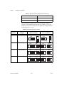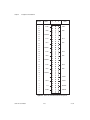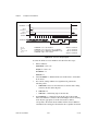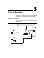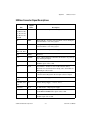
1
SCXI TM SCXI-1121 User Manual SCXI-1121 User Manual April 2010 373143A-01 Support Worldwide Technical Support and Product Information ni.com National Instruments Corporate Headquarters 11500 North Mopac Expressway Austin, Texas 78759-3504 USA Tel: 512 683 0100 Worldwide Offices Australia 1800 300 800, Austria 43 662 457990-0, Belgium 32 (0) 2 757 0020, Brazil 55 11 3262 3599, Canada 800 433 3488, China 86 21 5050 9800, Czech Republic 420 224 235 774, Denmark 45 45 76 26 00, Finland 358 (0) 9 725 72511, France 01 57 66 24 24, Germany 49 89 7413130, India 91 80 41190000, Israel 972 3 6393737, Italy 39 02 41309277, Japan 0120-527196, Korea 82 02 3451 3400, Lebanon 961 (0) 1 33 28 28, Malaysia 1800 887710, Mexico 01 800 010 0793, Netherlands 31 (0) 348 433 466, New Zealand 0800 553 322, Norway 47 (0) 66 90 76 60, Poland 48 22 328 90 10, Portugal 351 210 311 210, Russia 7 495 783 6851, Singapore 1800 226 5886, Slovenia 386 3 425 42 00, South Africa 27 0 11 805 8197, Spain 34 91 640 0085, Sweden 46 (0) 8 587 895 00, Switzerland 41 56 2005151, Taiwan 886 02 2377 2222, Thailand 662 278 6777, Turkey 90 212 279 3031, United Kingdom 44 (0) 1635 523545 For further support information, refer to the Technical Support Information document. To comment on National Instruments documentation, refer to the National Instruments Web site at ni.com/info and enter the Info Code feedback. © 1992–2010 National Instruments Corporation. All rights reserved. Important Information Warranty The SCXI-1121 is warranted against defects in materials and workmanship for a period of one year from the date of shipment, as evidenced by receipts or other documentation. National Instruments will, at its option, repair or replace equipment that proves to be defective during the warranty period. This warranty includes parts and labor. The media on which you receive National Instruments software are warranted not to fail to execute programming instructions, due to defects in materials and workmanship, for a period of 90 days from date of shipment, as evidenced by receipts or other documentation. National Instruments will, at its option, repair or replace software media that do not execute programming instructions if National Instruments receives notice of such defects during the warranty period. National Instruments does not warrant that the operation of the software shall be uninterrupted or error free. A Return Material Authorization (RMA) number must be obtained from the factory and clearly marked on the outside of the package before any equipment will be accepted for warranty work. National Instruments will pay the shipping costs of returning to the owner parts which are covered by warranty. National Instruments believes that the information in this document is accurate. The document has been carefully reviewed for technical accuracy. In the event that technical or typographical errors exist, National Instruments reserves the right to make changes to subsequent editions of this document without prior notice to holders of this edition. The reader should consult National Instruments if errors are suspected. In no event shall National Instruments be liable for any damages arising out of or related to this document or the information contained in it. EXCEPT AS SPECIFIED HEREIN, NATIONAL INSTRUMENTS MAKES NO WARRANTIES, EXPRESS OR IMPLIED, AND SPECIFICALLY DISCLAIMS ANY WARRANTY OF MERCHANTABILITY OR FITNESS FOR A PARTICULAR PURPOSE. CUSTOMER’S RIGHT TO RECOVER DAMAGES CAUSED BY FAULT OR NEGLIGENCE ON THE PART OF NATIONAL INSTRUMENTS SHALL BE LIMITED TO THE AMOUNT THERETOFORE PAID BY THE CUSTOMER. NATIONAL INSTRUMENTS WILL NOT BE LIABLE FOR DAMAGES RESULTING FROM LOSS OF DATA, PROFITS, USE OF PRODUCTS, OR INCIDENTAL OR CONSEQUENTIAL DAMAGES, EVEN IF ADVISED OF THE POSSIBILITY THEREOF. This limitation of the liability of National Instruments will apply regardless of the form of action, whether in contract or tort, including negligence. Any action against National Instruments must be brought within one year after the cause of action accrues. National Instruments shall not be liable for any delay in performance due to causes beyond its reasonable control. The warranty provided herein does not cover damages, defects, malfunctions, or service failures caused by owner’s failure to follow the National Instruments installation, operation, or maintenance instructions; owner’s modification of the product; owner’s abuse, misuse, or negligent acts; and power failure or surges, fire, flood, accident, actions of third parties, or other events outside reasonable control. Copyright Under the copyright laws, this publication may not be reproduced or transmitted in any form, electronic or mechanical, including photocopying, recording, storing in an information retrieval system, or translating, in whole or in part, without the prior written consent of National Instruments Corporation. National Instruments respects the intellectual property of others, and we ask our users to do the same. NI software is protected by copyright and other intellectual property laws. Where NI software may be used to reproduce software or other materials belonging to others, you may use NI software only to reproduce materials that you may reproduce in accordance with the terms of any applicable license or other legal restriction. Trademarks CVI, LabVIEW, National Instruments, NI, ni.com, the National Instruments corporate logo, and the Eagle logo are trademarks of National Instruments Corporation. Refer to the Trademark Information at ni.com/trademarks for other National Instruments trademarks. The mark LabWindows is used under a license from Microsoft Corporation. Windows is a registered trademark of Microsoft Corporation in the United States and other countries. Other product and company names mentioned herein are trademarks or trade names of their respective companies. Members of the National Instruments Alliance Partner Program are business entities independent from National Instruments and have no agency, partnership, or joint-venture relationship with National Instruments. Patents For patents covering National Instruments products/technology, refer to the appropriate location: Help»Patents in your software, the patents.txt file on your media, or the National Instruments Patent Notice at ni.com/patents. WARNING REGARDING USE OF NATIONAL INSTRUMENTS PRODUCTS (1) NATIONAL INSTRUMENTS PRODUCTS ARE NOT DESIGNED WITH COMPONENTS AND TESTING FOR A LEVEL OF RELIABILITY SUITABLE FOR USE IN OR IN CONNECTION WITH SURGICAL IMPLANTS OR AS CRITICAL COMPONENTS IN ANY LIFE SUPPORT SYSTEMS WHOSE FAILURE TO PERFORM CAN REASONABLY BE EXPECTED TO CAUSE SIGNIFICANT INJURY TO A HUMAN. (2) IN ANY APPLICATION, INCLUDING THE ABOVE, RELIABILITY OF OPERATION OF THE SOFTWARE PRODUCTS CAN BE IMPAIRED BY ADVERSE FACTORS, INCLUDING BUT NOT LIMITED TO FLUCTUATIONS IN ELECTRICAL POWER SUPPLY, COMPUTER HARDWARE MALFUNCTIONS, COMPUTER OPERATING SYSTEM SOFTWARE FITNESS, FITNESS OF COMPILERS AND DEVELOPMENT SOFTWARE USED TO DEVELOP AN APPLICATION, INSTALLATION ERRORS, SOFTWARE AND HARDWARE COMPATIBILITY PROBLEMS, MALFUNCTIONS OR FAILURES OF ELECTRONIC MONITORING OR CONTROL DEVICES, TRANSIENT FAILURES OF ELECTRONIC SYSTEMS (HARDWARE AND/OR SOFTWARE), UNANTICIPATED USES OR MISUSES, OR ERRORS ON THE PART OF THE USER OR APPLICATIONS DESIGNER (ADVERSE FACTORS SUCH AS THESE ARE HEREAFTER COLLECTIVELY TERMED “SYSTEM FAILURES”). ANY APPLICATION WHERE A SYSTEM FAILURE WOULD CREATE A RISK OF HARM TO PROPERTY OR PERSONS (INCLUDING THE RISK OF BODILY INJURY AND DEATH) SHOULD NOT BE RELIANT SOLELY UPON ONE FORM OF ELECTRONIC SYSTEM DUE TO THE RISK OF SYSTEM FAILURE. TO AVOID DAMAGE, INJURY, OR DEATH, THE USER OR APPLICATION DESIGNER MUST TAKE REASONABLY PRUDENT STEPS TO PROTECT AGAINST SYSTEM FAILURES, INCLUDING BUT NOT LIMITED TO BACK-UP OR SHUT DOWN MECHANISMS. BECAUSE EACH END-USER SYSTEM IS CUSTOMIZED AND DIFFERS FROM NATIONAL INSTRUMENTS' TESTING PLATFORMS AND BECAUSE A USER OR APPLICATION DESIGNER MAY USE NATIONAL INSTRUMENTS PRODUCTS IN COMBINATION WITH OTHER PRODUCTS IN A MANNER NOT EVALUATED OR CONTEMPLATED BY NATIONAL INSTRUMENTS, THE USER OR APPLICATION DESIGNER IS ULTIMATELY RESPONSIBLE FOR VERIFYING AND VALIDATING THE SUITABILITY OF NATIONAL INSTRUMENTS PRODUCTS WHENEVER NATIONAL INSTRUMENTS PRODUCTS ARE INCORPORATED IN A SYSTEM OR APPLICATION, INCLUDING, WITHOUT LIMITATION, THE APPROPRIATE DESIGN, PROCESS AND SAFETY LEVEL OF SUCH SYSTEM OR APPLICATION. Compliance Electromagnetic Compatibility Information This hardware has been tested and found to comply with the applicable regulatory requirements and limits for electromagnetic compatibility (EMC) as indicated in the hardware’s Declaration of Conformity (DoC)1. These requirements and limits are designed to provide reasonable protection against harmful interference when the hardware is operated in the intended electromagnetic environment. In special cases, for example when either highly sensitive or noisy hardware is being used in close proximity, additional mitigation measures may have to be employed to minimize the potential for electromagnetic interference. While this hardware is compliant with the applicable regulatory EMC requirements, there is no guarantee that interference will not occur in a particular installation. To minimize the potential for the hardware to cause interference to radio and television reception or to experience unacceptable performance degradation, install and use this hardware in strict accordance with the instructions in the hardware documentation and the DoC1. If this hardware does cause interference with licensed radio communications services or other nearby electronics, which can be determined by turning the hardware off and on, you are encouraged to try to correct the interference by one or more of the following measures: • Reorient the antenna of the receiver (the device suffering interference). • Relocate the transmitter (the device generating interference) with respect to the receiver. • Plug the transmitter into a different outlet so that the transmitter and the receiver are on different branch circuits. Some hardware may require the use of a metal, shielded enclosure (windowless version) to meet the EMC requirements for special EMC environments such as, for marine use or in heavy industrial areas. Refer to the hardware’s user documentation and the DoC1 for product installation requirements. When the hardware is connected to a test object or to test leads, the system may become more sensitive to disturbances or may cause interference in the local electromagnetic environment. Operation of this hardware in a residential area is likely to cause harmful interference. Users are required to correct the interference at their own expense or cease operation of the hardware. Changes or modifications not expressly approved by National Instruments could void the user’s right to operate the hardware under the local regulatory rules. 1 The Declaration of Conformity (DoC) contains important EMC compliance information and instructions for the user or installer. To obtain the DoC for this product, visit ni.com/certification, search by model number or product line, and click the appropriate link in the Certification column. Contents About This Manual Conventions ...................................................................................................................xi Related Documentation..................................................................................................xii Chapter 1 Introduction What Your Kit Should Contain .....................................................................................1-2 Optional Software ..........................................................................................................1-2 Optional Equipment .......................................................................................................1-4 Custom Cables.................................................................................................1-5 Unpacking ......................................................................................................................1-6 Chapter 2 Configuration and Installation Module Configuration....................................................................................................2-1 Digital Signal Connections..............................................................................2-4 Jumper W44 ......................................................................................2-4 Jumper W38 ......................................................................................2-5 Jumper W32 ......................................................................................2-5 Using Jumpers W32 and W38 ..........................................................2-5 Analog Configuration......................................................................................2-7 Grounding, Shielding, and Reference Mode Selection.....................2-7 Input Channel Jumpers......................................................................2-9 Excitation Jumpers............................................................................2-10 Hardware Installation.....................................................................................................2-14 Signal Connections ........................................................................................................2-15 Front Connector...............................................................................................2-15 Front Connector Signal Descriptions ..............................................................2-17 Analog Input Channels......................................................................2-19 Excitation Channels ..........................................................................2-21 Temperature Sensor Connection .......................................................2-21 Connector-and-Shell Assembly ........................................................2-22 SCXI-1320, SCXI-1328, and SCXI-1321 Terminal Blocks.............2-23 Rear Signal Connector.....................................................................................2-36 Rear Signal Connector Signal Descriptions ....................................................2-37 Analog Output Signal Connections...................................................2-38 Digital I/O Signal Connections .........................................................2-39 Timing Requirements and Communication Protocol........................2-40 Communication Signals ....................................................................2-41 © National Instruments Corporation v SCXI-1121 User Manual Contents Chapter 3 Theory of Operation Functional Overview ..................................................................................................... 3-1 SCXIbus Connector ........................................................................................ 3-3 SCXIbus Connector Signal Descriptions........................................................ 3-4 Digital Interface............................................................................................................. 3-6 Digital Control Circuitry ............................................................................................... 3-7 Analog and Timing Circuitry ........................................................................................ 3-8 Analog Input Channels.................................................................................... 3-8 Excitation Output Channels ............................................................................ 3-11 Calibration....................................................................................................... 3-11 Analog Output Circuitry ................................................................................. 3-12 Scanning Modes ............................................................................................................ 3-14 Single-Module Parallel Scanning.................................................................... 3-14 Multiplexed Scanning ..................................................................................... 3-14 Single-Module Multiplexed Scanning.............................................. 3-15 Multiple-Module Multiplexed Scanning .......................................... 3-16 Multiple-Chassis Scanning ............................................................... 3-17 Chapter 4 Register Descriptions Register Description ...................................................................................................... 4-1 Register Description Format ........................................................................... 4-1 SCXI-1121 Registers ...................................................................................... 4-1 Slot 0 Register Descriptions............................................................................ 4-5 Chapter 5 Programming Programming Considerations ........................................................................................ 5-1 Notation........................................................................................................... 5-1 Register Writes................................................................................................ 5-1 Register Selection and Write Procedure ........................................... 5-2 Initialization...................................................................................... 5-4 Single-Channel Measurements ....................................................................... 5-4 Direct Measurements ........................................................................ 5-4 Indirect Measurements ..................................................................... 5-5 Scanning Measurements ................................................................................. 5-7 1. Data Acquisition Board Setup Programming ............................... 5-7 2. Module Programming................................................................... 5-10 3. Programming the Slot 0 Hardscan Circuitry ................................ 5-13 4. Acquisition Enable, Triggering, and Servicing ............................ 5-15 SCXI-1121 User Manual vi ni.com Contents Scanning Examples........................................................................................................5-15 Example 1........................................................................................................5-15 Example 2........................................................................................................5-16 Example 3........................................................................................................5-17 Appendix A Specifications Appendix B Rear Signal Connector Appendix C SCXIbus Connector Appendix D SCXI-1121 Front Connector Appendix E SCXI-1121 Cabling Appendix F Revision A and B Photo and Parts Locator Diagrams Glossary Index Figures Figure 2-1. Figure 2-2. Figure 2-3. Figure 2-4. Figure 2-5. Figure 2-6. Figure 2-7. SCXI-1121 General Parts Locator Diagram .........................................2-2 SCXI-1121 Detailed Parts Locator Diagram.........................................2-3 SCXI-1121 Front Connector Pin Assignment.......................................2-16 Ground-Referenced Signal Connection with High Common-Mode Voltage ..................................................................................................2-19 Floating Signal Connection Referenced to Chassis Ground for Better Signal-to-Noise Ratio .................................................................2-19 Floating AC-Coupled Signal Connection..............................................2-20 AC-Coupled Signal Connection with High Common-Mode Voltage...2-20 © National Instruments Corporation vii SCXI-1121 User Manual Contents Figure 2-8. Figure 2-9. Figure 2-10. Figure 2-11. Figure 2-12. Figure 2-13. Figure 2-14. Figure 2-15. Figure 2-16. Figure 2-17. Figure 2-18. Figure 2-19. Assembling and Mounting the SCXI-1330 Connector-and-Shell Assembly............................................................................................... 2-23 Nulling Circuit ...................................................................................... 2-27 Shunt Circuit ......................................................................................... 2-28 SCXI-1320 Parts Locator Diagram....................................................... 2-33 SCXI-1328 Parts Locator Diagram....................................................... 2-34 SCXI-1321 Parts Locator Diagram....................................................... 2-35 SCXI-1121 Rear Signal Connector Pin Assignment ............................ 2-36 SCANCLK Timing Requirements ........................................................ 2-41 Slot-Select Timing Diagram ................................................................. 2-42 Serial Data Timing Diagram ................................................................. 2-43 Configuration Register Write Timing Diagram .................................... 2-44 SCXI-1121 Module ID Register Timing Diagram ............................... 2-45 Figure 3-1. Figure 3-2. Figure 3-3. Figure 3-4. Figure 3-5. Figure 3-6. Figure 3-7. Figure 3-8. Figure 3-9. Figure 3-10. Figure 3-11. SCXI-1121 Block Diagram................................................................... 3-1 SCXIbus Connector Pin Assignment.................................................... 3-3 Digital Interface Circuitry Block Diagram ........................................... 3-6 SCXI-1121 Digital Control................................................................... 3-7 Analog Input Block Diagram................................................................ 3-9 Analog Output Circuitry ....................................................................... 3-12 Single-Module Parallel Scanning ......................................................... 3-14 Single-Module Multiplexed Scanning (Direct) .................................... 3-15 Single-Module Multiplexed Scanning (Indirect) .................................. 3-16 Multiple-Module Multiplexed Scanning............................................... 3-16 Multiple-Chassis Scanning ................................................................... 3-17 Figure B-1. SCXI-1121 Rear Signal Connector Pin Assignment ............................ B-1 Figure C-1. SCXIbus Connector Pin Assignment.................................................... C-2 Figure D-1. SCXI-1121 Front Connector Pin Assignment ...................................... D-2 Figure E-1. Figure E-2. Figure E-3. Figure E-4. SCXI-1340 Installation ......................................................................... E-4 SCXI-1180 Rear Connections............................................................... E-9 SCXI-1180 Front Panel Installation...................................................... E-10 Cover Removal ..................................................................................... E-11 Figure F-1. Figure F-2. Figure F-3. Revision A and B SCXI-1121 Signal Conditioning Module................ F-1 Revision A and B SCXI-1121 General Parts Locator Diagram ........... F-2 Revision A and B SCXI-1121 Detailed Parts Locator Diagram........... F-3 SCXI-1121 User Manual viii ni.com Contents Tables Table 2-1. Table 2-2. Table 2-3. Table 2-4. Table 2-5. Table 2-6. Table 2-7. Table 2-8. Table 2-9. Table 2-10. Table 2-11. Table 2-12. Table 2-13. Table 2-14. Table 2-15. Table 2-16. Digital Signal Connections, Jumper Settings .......................................2-6 Jumper W33 Settings.............................................................................2-8 Gain Jumper Allocation.........................................................................2-9 Gain Jumper Positions...........................................................................2-9 Filter Jumper Allocation........................................................................2-10 Voltage and Current Mode Excitation Jumper Setup............................2-11 Maximum Load per Excitation Channel ..............................................2-11 Excitation Level Jumper Selection .......................................................2-12 Completion Network Jumpers ..............................................................2-13 Trimmer Potentiometer and Corresponding Channel ...........................2-25 Nulling Resistors and Corresponding Channel .....................................2-25 Jumper Settings of the Nulling Circuits ...............................................2-27 Jumper Settings on the SCXI-1320 Terminal Block.............................2-31 Jumper Settings on the SCXI-1328 Terminal Block.............................2-31 Jumper Settings on the SCXI-1321 Terminal Block.............................2-32 SCXIbus to SCXI-1121 Rear Signal Connector to Data Acquisition Board Pin Equivalences.........................................................................2-40 Table 3-1. SCXIbus Equivalents for the Rear Signal Connector ...........................3-5 Table 5-1. SCXI-1121 Rear Signal Connector Pin Equivalences ..........................5-2 Table E-1. Table E-2. Table E-3. Table E-4. SCXI-1121 and MIO-16 Pinout Equivalences .....................................E-2 SCXI-1341 and SCXI-1344 Pin Translations ......................................E-5 SCXI-1342 Pin Translations ................................................................E-7 SCXI-1343 Pin Connections ................................................................E-14 © National Instruments Corporation ix SCXI-1121 User Manual About This Manual This manual describes the electrical and mechanical aspects of the SCXI-1121 and contains information concerning its operation and programming. The SCXI-1121 is a member of the National Instruments Signal Conditioning eXtensions for Instrumentation (SCXI) Series for the National Instruments data acquisition plug-in boards. This board is designed for signal conditioning of strain gauges, RTDs, thermistors, thermocouples, volt and millivolt sources, and 4 to 20 mA sources or 0 to 20 mA process-current sources where high common-mode voltages exist. The SCXI-1121 operates as four isolated input channels and four isolated excitation channels. Each channel is isolated and independently configurable via jumpers. This manual describes the installation, basic programming considerations, and theory of operation for the SCXI-1121. Conventions The following conventions appear in this manual: <> Angle brackets that contain numbers separated by an ellipsis represent a range of values associated with a bit or signal name—for example, AO <3..0>. » The » symbol leads you through nested menu items and dialog box options to a final action. The sequence File»Page Setup»Options directs you to pull down the File menu, select the Page Setup item, and select Options from the last dialog box. This icon denotes a note, which alerts you to important information. This icon denotes a caution, which advises you of precautions to take to avoid injury, data loss, or a system crash. When this symbol is marked on a product, refer to the Read Me First: Safety and Electromagnetic Compatibility for information about precautions to take. bold Bold text denotes items that you must select or click in the software, such as menu items and dialog box options. Bold text also denotes parameter names. © National Instruments Corporation xi SCXI-1121 User Manual About This Manual italic Italic text denotes variables, emphasis, a cross-reference, or an introduction to a key concept. Italic text also denotes text that is a placeholder for a word or value that you must supply. monospace Text in this font denotes text or characters that you should enter from the keyboard, sections of code, programming examples, and syntax examples. This font is also used for the proper names of disk drives, paths, directories, programs, subprograms, subroutines, device names, functions, operations, variables, filenames, and extensions. Related Documentation The following documents contain information that you may find helpful as you read this manual: SCXI-1121 User Manual • AT-MIO-16 User Manual (part number 320476-01) • AT-MIO-16D User Manual (part number 320489-01) • AT-MIO-16F-5 User Manual (part number 320266-01) • AT-MIO-16X User Manual (part number 320488-01) • AT-MIO-64F-5 User Manual (part number 320487-01) • Lab-LC User Manual (part number 320380-01) • Lab-NB User Manual (part number 320174-01) • Lab-PC User Manual (part number 320205-01) • Lab-PC+ User Manual (part number 320502-01) • MC-MIO-16 User Manual, Revisions A to C (part number 320130-01) • MC-MIO-16 User Manual, Revision D (part number 320560-01) • NB-MIO-16 User Manual (part number 320295-01) • NB-MIO-16X User Manual (part number 320157-01) • PC-LPM-16 User Manual (part number 320287-01) • SCXI Chassis User Manual (part number 374423L-01, 320423L-01) • Technical Support Information (part number 373541E-01) • Read Me First: Safety and Electromagnetic Compatibility (part number 373332E-01) xii ni.com 1 Introduction This chapter describes the SCXI-1121; lists the contents of your SCXI-1121 kit; describes the optional software, optional equipment, and custom cables; and explains how to unpack the SCXI-1121 kit. The SCXI-1121 consists of four isolated input channels and four isolated excitation channels. The SCXI-1121 is a module for signal conditioning of strain gauges, RTDs, thermistors, thermocouples, volt and millivolt sources, 4 to 20 mA current sources, and 0 to 20 mA process-current sources. The SCXI-1121 can operate in two output modes—the Parallel-Output mode with all four input channels connected in parallel to four data acquisition board channels, or the Multiplexed-Output mode with all four channels multiplexed into a single data acquisition board channel. The SCXI-1121 operates with full functionality with National Instruments MIO-16 boards. The SCXI-1121 operates with full functionality with the Lab-PC+ board in single-chassis SCXI systems. However, the Lab-PC+ cannot control multiple-chassis SCXI systems. You can use the Lab-NB, the Lab-PC, the Lab-LC, and the PC-LPM-16 boards with the SCXI-1121, but these boards can control only single-chassis SCXI systems and cannot scan the module when it is configured in the Multiplexed-Output mode. These boards can perform only single-channel reads in this mode. You can also use the SCXI-1121 with other systems that comply with the specifications given in Chapter 2, Configuration and Installation. You can multiplex several SCXI-1121s into a single channel, thus greatly increasing the number of analog input signals that can be digitized. The addition of a shielded terminal block provides screw terminals for easy signal attachment to the SCXI-1121. In addition, a temperature sensor for cold-junction compensation of thermocouples is included on the terminal block. This cold-junction reference (CJR) is either multiplexed along with the four input channels or connected by jumpers to a different channel of the data acquisition board. With the SCXI-1121, the SCXI chassis can serve as a fast-scanning signal conditioner for laboratory testing, production testing, and industrial process monitoring. © National Instruments Corporation 1-1 SCXI-1121 User Manual Chapter 1 Introduction What Your Kit Should Contain The contents of the SCXI-1121 kit (part number 776572-21) are listed as follows: Kit Component SCXI-1121 module Part Number 181700-01 SCXI-1121 User Manual 320426D-01 If your kit is missing any of the components, contact National Instruments. Optional Software This manual contains complete instructions for directly programming the SCXI-1121. You can order separate software packages for controlling the SCXI-1121 from National Instruments. When you combine the PC, AT, and MC data acquisition boards with the SCXI-1121, you can use LabVIEW for Windows or LabWindows for DOS. LabVIEW and LabWindows are innovative program development software packages for data acquisition and control applications. LabVIEW uses graphical programming, whereas LabWindows enhances Microsoft C and QuickBASIC. Both packages include extensive libraries for data acquisition, instrument control, data analysis, and graphical data presentation. Your National Instruments data acquisition board is shipped with the NI-DAQ software. NI-DAQ has a library of functions that you can call from your application programming environment. These functions include routines for analog input (A/D conversion), buffered data acquisition (high-speed A/D conversion), analog output (D/A conversion), waveform generation, digital I/O, counter/timer, SCXI, RTSI, and self-calibration. NI-DAQ maintains a consistent software interface among its different versions so you can switch between platforms with minimal modifications to your code. SCXI-1121 User Manual 1-2 ni.com Chapter 1 Introduction You can also use the SCXI-1121, together with the PC, AT, and MC data acquisition boards, with NI-DAQ software for DOS/Windows/ LabWindows™/CVI™. NI-DAQ software for DOS/Windows/ LabWindows/CVI comes with language interfaces for Professional BASIC, Turbo Pascal, Turbo C, Turbo C++, Borland C++, and Microsoft C for DOS and Visual Basic, Turbo Pascal, Microsoft C with SDK, and Borland C++ for Windows. NI-DAQ software for DOS/Windows/LabWindows is on high-density 5.25 in. and 3.5 in. diskettes. You can use the SCXI-1121, together with the Lab-LC or NB Series data acquisition boards, with LabVIEW for Macintosh, a software system that features interactive graphics, a state-of-the-art user interface, and a powerful graphical programming language. The LabVIEW Data Acquisition VI Library, a series of VIs for using LabVIEW with National Instruments boards, is included with LabVIEW. The LabVIEW Data Acquisition VI Library is functionally equivalent to the NI-DAQ software for Macintosh. You can also use the SCXI-1121, combined with the NB Series data acquisition boards, with NI-DAQ software for Macintosh. NI-DAQ software for Macintosh, which is shipped with all National Instruments Macintosh data acquisition boards, comes with language interfaces for MPW C, THINK C, Pascal, and Microsoft QuickBASIC. Any language that uses Device Manager Toolbox calls can access NI-DAQ software for Macintosh. © National Instruments Corporation 1-3 SCXI-1121 User Manual Chapter 1 Introduction Optional Equipment Equipment Part Number NB6 cable 0.5 m 1.0 m 181305-01 181305-10 SCXI-1320 front terminal block 776573-20 SCXI-1321 offset-null and shunt-calibration terminal block 776573-21 SCXI-1328 high-accuracy isothermal terminal block 776573-28 SCXI-1330 32-pin connector-and-shell assembly 776573-30 SCXI-1340 cable assembly 776574-40 SCXI-1341 Lab-NB/Lab-PC/Lab-PC+ cable assembly 776574-41 SCXI-1342 PC-LPM-16 cable assembly 776574-42 SCXI-1343 rear screw terminal adapter 776574-43 SCXI-1344 Lab-LC cable assembly 776574-44 SCXI-1346 shielded multichassis cable adapter 776574-46 SCXI-1347 SCXI shielded cable assembly with 1 m cable with 2 m cable with 5 m cable with 10 m cable 776574-471 776574-472 776574-475 776574-470 SCXI-1349 SCXI shielded cable assembly with 1 m cable with 2 m cable with 5 m cable with 10 m cable 776574-491 776574-492 776574-495 776574-490 SCXI-1350 multichassis adapter 776575-50 SCXI process-current resistor kit 776582-01 Standard ribbon cable 0.5 m 1.0 m 180524-05 180524-10 Refer to the Signal Connections section in Chapter 2, Configuration and Installation, and to Appendix E, SCXI-1121 Cabling, for additional information on cabling, connectors, and adapters. SCXI-1121 User Manual 1-4 ni.com Chapter 1 Introduction Custom Cables The SCXI-1121 rear signal connector is a 50-pin male ribbon-cable header. The manufacturer part number used by National Instruments for this header is as follows: • AMP Inc. (part number 1-103310-0) The mating connector for the SCXI-1121 rear signal connector is a 50-position polarized ribbon-socket connector with strain relief. National Instruments uses a polarized or keyed connector to prevent inadvertent upside-down connection to the SCXI-1121. Recommended manufacturer part numbers for this mating connector are as follows: • Electronic Products Division/3M (part number 3425-7650) • T&B/Ansley Corporation (part number 609-5041CE) Standard 50-conductor, 28 AWG, stranded ribbon cables that can be used with these connectors are as follows: • Electronic Products Division/3M (part number 3365/50) • T&B/Ansley Corporation (part number 171-50) The SCXI-1121 front connector is a 32-pin DIN C male connector with column A and column C even pins only. The manufacturer part number used by National Instruments for this connector is as follows: • Panduit Corporation (part number 100-932-023) The mating connector for the SCXI-1121 front connector is a 32-pin DIN C female connector. National Instruments uses a polarized connector to prevent inadvertent upside-down connection to the SCXI-1121. Recommended manufacturer part numbers for this mating connector are as follows: • Panduit Corporation (part number 100-932-434 straight-solder eyelet pins) • Panduit Corporation (part number 100-932-633; right-angle pins) National Instruments selected these connectors to meet UL 1950 and UL 1244 for 1,500 Vrms isolation. © National Instruments Corporation 1-5 SCXI-1121 User Manual Chapter 1 Introduction Unpacking Your SCXI-1121 module is shipped in an antistatic package to prevent electrostatic damage to the module. Several components on the module can be damaged by electrostatic discharge. To avoid such damage in handling the module, take the following precautions: SCXI-1121 User Manual • Touch the antistatic package to a metal part of your SCXI chassis before removing the module from the package. • Remove the module from the package and inspect the module for loose components or any other sign of damage. Notify National Instruments if the module appears damaged in any way. Do not install a damaged module into your SCXI chassis. 1-6 ni.com Configuration and Installation 2 This chapter describes the SCXI-1121 jumper configurations, installation of the SCXI-1121 into the SCXI chassis, signal connections to the SCXI-1121, and cable wiring. Module Configuration The SCXI-1121 contains 49 jumpers that are shown in the parts locator diagrams in Figures 2-1 and 2-2. © National Instruments Corporation 2-1 SCXI-1121 User Manual Chapter 2 Configuration and Installation Figure 2-1. SCXI-1121 General Parts Locator Diagram SCXI-1121 User Manual 2-2 ni.com Chapter 2 Configuration and Installation Figure 2-2. SCXI-1121 Detailed Parts Locator Diagram The jumpers are used as follows: • • © National Instruments Corporation Fixed jumpers – On Revision A and B modules, jumper W32 is unused and should not be connected. – Jumper W45 is reserved and should not be reconfigured. – On Revision A and B modules, jumper W44 carries the SLOT0SEL* signal from the rear signal connector, after buffering, to the SCXIbus INTR* line and should be left in the factory-set position (position 1). On Revision C or later modules, jumper W44 does not exist. User-configurable jumper – Jumper W38 carries the SCXIbus MISO line, after buffering, to the SERDATOUT signal on the rear signal connector. – On Revision C or later modules, jumper W32 connects a pullup resistor to the SERDATOUT signal on the rear signal connector. – Jumper W33 configures the guard, the analog output ground, and enables the Pseudodifferential Reference mode. 2-3 SCXI-1121 User Manual Chapter 2 Configuration and Installation – Jumpers W3, W19, W29, and W41 configure the first-stage gain of input channels 0 through 3, respectively. – Jumpers W4, W20, W30, and W42 configure the second-stage gain of input channels 0 through 3, respectively. – Jumpers W5, W21, W31, and W43 configure the first-stage filtering of input channels 0 through 3, respectively. – Jumpers W6 and W7, W8 and W9, W10 and W11, and W12 and W13 configure the second-stage filtering of input channels 0 through 3, respectively. – Jumpers W14 and W15, W22 and W23, W34 and W35, and W46 and W47 configure the voltage or current mode of operation for excitation channels 0 through 3, respectively. – Jumpers W16 and W26, W24 and W25, W36 and W37, and W48 and W49 configure the level of excitation for excitation channels 0 through 3, respectively. – Jumpers W1 and W2, W17 and W18, W27 and W28, and W39 and W40 configure the half-bridge completion network for channels 0 through 3, respectively. Further configuration of the board is software controlled and will be discussed later in this chapter. Digital Signal Connections The SCXI-1121 has three jumpers dedicated for communication between the data acquisition board and the SCXIbus. These jumpers are W32, W38, and W44. Jumper W44 Position 1 on Revision A and B modules connects, after buffering, SLOT0SEL* to the SCXIbus INTR* line. This is the factory-default setting and should not be changed. In this setting, the data acquisition board controls the SCXIbus INTR* line. Refer to the Timing Requirements and Communication Protocol section later in this chapter, and Chapter 5, Programming, for information on the use of the INTR* line. Refer to Appendix E, SCXI-1121 Cabling, for the pin equivalences of the SCXI-1121 rear signal connector and the data acquisition board I/O connector. Position 3 is reserved and should not be used. This position is not explicitly marked on the module. SCXI-1121 User Manual 2-4 ni.com Chapter 2 Configuration and Installation On Revision C or later modules, jumper W44 does not exist. SLOT0SEL* is always buffered to the INTR* line. Jumper W38 Position 1 connects, after buffering, the SCXIbus MISO line to the SERDATOUT pin of the rear signal connector. In this setting, along with the proper setting of W32, the data acquisition board can read the Module ID Register of the SCXI-1121. Refer to the Timing Requirements and Communication Protocol section later in this chapter, and Chapter 4, Register Descriptions, for information on reading the Module ID Register. Refer to Appendix E, SCXI-1121 Cabling, for the pin equivalences of the SCXI-1121 rear signal connector and the data acquisition board I/O connector. This is the factory-default setting. Position 3 disconnects SERDATOUT from the SCXIbus MISO line. Jumper W32 On Revision A and B modules, jumper W32 should not be connected. On Revision C or later modules, Position 1 connects a 2.2 kΩ pull-up resistor to the SERDATOUT line (factory-default setting), and Position 3 does not connect the pull-up resistor to the SERDATOUT line. Using Jumpers W32 and W38 Set jumpers W32 and W38 as follows: If the SCXI-1121 is not cabled to a data acquisition board, the positions of these jumpers do not matter, so leave them in their factory default positions (both in position 1). If the SCXI-1121 is cabled to a data acquisition board, and the SCXI chassis that the SCXI-1121 is in, is the only SCXI chassis cabled to that data acquisition board, leave the jumpers in their factory default positions (both in position 1). If the SCXI-1121 is cabled to a data acquisition board, and there are multiple SCXI chassis cabled to that data acquisition board with shielded cables (you are using SCXI-1346 shielded cable multi-chassis adapters), leave the jumpers in their factory default positions (both in position 1). If the SCXI-1121 is cabled to a data acquisition board, and there are multiple SCXI chassis cabled to that data acquisition board with ribbon cables (you are using SCXI-1350 multi-chassis adapters), leave jumper © National Instruments Corporation 2-5 SCXI-1121 User Manual Chapter 2 Configuration and Installation W38 in its factory default position (position 1). On all but one of the SCXI-1121s that are cabled to the data acquisition board, move jumper W32 to position 3. It does not matter which of the SCXI-1121 modules that are cabled to the data acquisition board has jumper W32 set to position 1. If you have different types of modules cabled to the data acquisition board, those different modules will have jumpers similar to W38 and W32 of the SCXI-1121. Set those jumpers on the different modules using the same method described here for the SCXI-1121. On Revision A and B SCXI-1121s, jumper W32 is not used. You set jumper W38 as explained in the cases above, except in the case of a multiple chassis ribbon cable system. In a multichassis ribbon cable system with Revision A and B SCXI-1121s cabled to the data acquisition board, you can access the MISO line in only one chassis. Pick one of the chassis and set jumper W38 to position 1 on the SCXI-1121 in that chassis that is cabled to the data acquisition board. On the SCXI-1121s that are in the other chassis and cabled to the data acquisition board, set jumper W38 to position 3. Notice that you will only be able to access digital information from the chassis that has the SCXI-1121 with jumper W38 set to position 1. Table 2-1. Digital Signal Connections, Jumper Settings Jumper W38 W38 W45 SCXI-1121 User Manual Description Factory setting; connects MISO to SERDATOUT Parking position Configuration 3 • 2 • 1 • 3 • 2 • 1 • 3 • 2 • 1 • Factory setting 2-6 ni.com Chapter 2 Configuration and Installation Table 2-1. Digital Signal Connections, Jumper Settings (Continued) Jumper W44 W32 W32 Description Factory setting (Revision A and B modules only) Configuration 3 • 2 • 1 • 3 • 2 • 1 • 3 • 2 • 1 • Fatory-default setting; connects pullup to SERDATOUT (Revision C and later) Parking position (not connected on Revision A or B modules) Analog Configuration The SCXI-1121 has 45 analog configuration jumpers. Before starting, notice that the jumper configurations for each input channel and each excitation channel are similar only the jumper numbers differ. Therefore, when you learn how to set up one channel pair (input and excitation), you can set up the other channel pairs as well. Grounding, Shielding, and Reference Mode Selection Jumper W33 Position AB-R0 connects the analog reference to the analog output ground (pins 1 and 2 on the rear signal connector). Select this configuration if you are using an RSE data acquisition board. It is not recommended to use a differential input data acquisition board when jumper W33 is in the AB-R0 position. Position AB-R1 connects the analog reference to the SCXIbus guard. Position A-R0R1 is the parking position and the factory setting. © National Instruments Corporation 2-7 SCXI-1121 User Manual Chapter 2 Configuration and Installation Position AB-R2 enables the Pseudodifferential Reference mode and connects the analog reference to the OUTREF pin on the rear signal connector. Select this mode when the SCXI-1121 has to operate with data acquisition boards that have a nonreferenced single-ended (NRSE) input. It is not recommended to use differential-input data acquisition boards when jumper W33 is in the AB-R2 position. Table 2-2. Jumper W33 Settings Jumper W33 W33 W33 W33 SCXI-1121 User Manual Description Factory setting in parking position Connects the analog reference to AOGND (pins 1 and 2 of the rear signal connector) Connects SCXIbus guard to the analog reference Enables the Pseudodifferential Reference mode (pin 19 of the rear signal connector is connected to the analog reference) 2-8 Configuration • • • A • • • B R2 R1 R0 • • • A • • • B R2 R1 R0 • • • A • • • B R2 R1 R0 • • • A • • • B R2 R1 R0 ni.com Chapter 2 Configuration and Installation Input Channel Jumpers Gain Jumpers Each input channel has two gain stages. The first gain stage provides gains of 1, 10, 50, and 100 and the second stage provides gains of 1, 2, 5, 10, and 20. Tables 2-3 and 2-4 show how to set up the gain for each channel. Table 2-3. Gain Jumper Allocation Input Channel Number First Gain Jumper Second Gain Jumper 0 W3 W4 1 W19 W20 2 W29 W30 3 W41 W42 The board is shipped to you with the first-stage gain set to 100 (position A) and a second-stage gain set to 10 (position D). To change the gain of your module, move the appropriate jumper on your module to the position indicated in Table 2-4. Refer to Figure 2-2 for the jumper locations on your module. To determine the overall gain of a given channel use the following formula: Overall gain = First-stage gain × second-stage gain Table 2-4. Gain Jumper Positions © National Instruments Corporation Gain Setting Jumper Position First-stage 1 10 50 100 D C B A (factory setting) Second-stage 1 2 5 10 20 A B C D (factory setting) E 2-9 SCXI-1121 User Manual Chapter 2 Configuration and Installation Filter Jumpers Two-stage filtering is also available on your SCXI-1121 module. The first stage is located in the isolated section of the input channel, whereas the second stage is located in the nonisolated section of the input channel. This permits a higher signal-to-noise ratio by eliminating the noise generated by the isolation amplifier. Furthermore, two filter bandwidths are available—10 kHz and 4 Hz. Table 2-5. Filter Jumper Allocation First Filter Jumper Second Filter Jumper Input Channel Number 4 Hz (Factory Setting) 10 kHz 4 Hz (Factory Setting) 10 kHz 0 W5-A W5-B W6 W7 1 W21-A W21-B W8 W9 2 W31-A W31-B W10 W11 3 W43-A W43-B W12 W13 Your SCXI-1121 is shipped in the 4 Hz configuration. Always make sure to set both stages to the same bandwidth. This will ensure that the required bandwidth is achieved. Excitation Jumpers Current and Voltage Excitation Jumpers You can configure each excitation channel of your SCXI-1121 to either a Voltage or Current excitation mode. Each channel has two jumpers for this purpose. Set both jumpers in the same mode for correct operation of the excitation channel. Refer to Table 2-6 for setting up your module in the mode you want. Your SCXI-1121 is shipped to you in the Voltage mode. SCXI-1121 User Manual 2-10 ni.com Chapter 2 Configuration and Installation Table 2-6. Voltage and Current Mode Excitation Jumper Setup Excitation Channel Jumpers 0 W14 and W15 W14 W15 • • • • • • • • • • 1 2 3 1 2 3 1 2 3 1 2 3 W22 and W23 W22 W23 W22 W23 • • • • • • • • • • • • 1 2 3 1 2 3 1 2 3 1 2 3 W34 and W35 W34 W35 W34 W35 • • • • • • • • • • • • 3 W15 • 2 W14 Current Mode • 1 Voltage Mode (Factory Setting) 1 2 3 1 2 3 1 2 3 1 2 3 W46 and W47 W46 W47 W46 W47 • • • • • • • • • • • • 1 2 3 1 2 3 1 2 3 1 2 3 Excitation Level Each excitation channel of your SCXI-1121 has two different current or voltage levels. You can set a given channel to one of the following level modes: • In the Current mode 0.150 or 0.450 mA • In the Voltage mode 3.333 or 10 V It is important to notice that you should select the level of excitation according to the load you are using. Table 2-7 lists the maximum load that can be driven per channel at each level of excitation for both volt and current excitation. Table 2-7. Maximum Load per Excitation Channel © National Instruments Corporation Excitation Level Maximum Load 3.333 V 28 mA 10 V 14 mA 2-11 SCXI-1121 User Manual Chapter 2 Configuration and Installation Table 2-7. Maximum Load per Excitation Channel (Continued) Excitation Level Maximum Load 0.150 mA 10 kΩ 0.450 mA 10 kΩ After selecting the excitation mode of operation desired—Voltage or Current—as described in the previous section, use Table 2-8 to set your SCXI-1121 for the level of operation. Your SCXI-1121 is shipped with the Voltage mode set to 3.333 V. Table 2-8. Excitation Level Jumper Selection Excitation Channel Jumpers 0 W16 and W26 3.333 V or 0.150 mA (Factory Setting) W26 2 3 3 W24 W25 • • 2 • 1 • • 1 • 2 • 3 3 • W24 W25 • • • • • • • • • • • 1 2 3 1 2 3 1 2 3 1 2 3 W36 and W37 W36 W37 W36 W37 • • • • • • • • • • • • 1 2 3 1 2 3 1 2 3 1 2 3 W48 and W49 W48 W49 W48 W49 • • • • • • • • • • • • SCXI-1121 User Manual • 1 • 3 • • 2 1 2 W24 and W25 W26 W16 • W16 1 10 V or 0.450 mA 1 2 3 1 2 3 1 2 3 1 2 3 2-12 ni.com Chapter 2 Configuration and Installation Using the Internal Half-Bridge Completion Your SCXI-1121 includes half-bridge completion for half-bridge and quarter-bridge setups. The completion network consists of two 4.5 kΩ ± 0.05% ratio tolerance resistors with a temperature coefficient of 5 ppm/°C. These resistors are connected in series. To enable the network, you must set two jumpers for each input/excitation channel pair. When the completion network is enabled, you cannot access the negative input of the amplifier, which preserves the overvoltage protection of the channel. Table 2-9 shows how to enable and disable the completion network. When using the half-bridge completion network with a quarter-bridge setup, you must use an extra resistor to complete the bridge. Place this resistor on the terminal block between the positive input channel and the negative excitation output. Note Table 2-9. Completion Network Jumpers Channel Jumpers 0 W1 and W2 Enable Completion • • • • A B Disable Network (Factory Setting) • • • • A B W2 • 1 2 • • • 3 • 2 W17 and W18 • • 1 W1 • • W18 © National Instruments Corporation W18 B A B 2 2-13 3 W17 • A • • • • • • • • 1 W1 3 1 2 • 1 • W2 W17 3 SCXI-1121 User Manual Chapter 2 Configuration and Installation Table 2-9. Completion Network Jumpers (Continued) Jumpers 2 W27 and W28 Enable Completion • Disable Network (Factory Setting) • • • W28 3 B 2 • W27 3 1 2 • • A • B • A • • • • • • 1 W39 and W40 W28 • • • W40 W40 B A B 2 3 W39 • A • • • • • • • • 1 W27 3 1 2 • Channel W39 3 Hardware Installation You can install the SCXI-1121 in any available SCXI chassis. After you have made any necessary changes and have verified and recorded the jumper settings, you are ready to install the SCXI-1121. The following are general installation instructions consult the user manual or technical reference manual of your SCXI chassis for specific instructions and cautions: SCXI-1121 User Manual 1. Turn off the computer that contains the data acquisition board or disconnect it from your SCXI chassis. 2. Turn off the SCXI chassis. Do not insert the SCXI-1121 into a chassis that is turned on. 3. Insert the SCXI-1121 into the board guides. Gently guide the module into the back of the slot until the connectors make good contact. If a cable assembly has already been installed in the rear of the chassis, the module and cable assembly must be firmly engaged; however, do not force the module into place. 4. Screw the front mounting panel of the SCXI-1121 to the top and bottom threaded strips of your SCXI chassis. 2-14 ni.com Chapter 2 5. Configuration and Installation If this module is to be connected to an MIO-16 data acquisition board, attach the connector at the metal end of the SCXI-1340 cable assembly to the rear signal connector on the SCXI-1121 module. Screw the rear panel to the rear threaded strip. Attach the loose end of the cable to the MIO-16 board. Note For installation procedures with other SCXI accessories and data acquisition boards, consult Appendix E, SCXI-1121 Cabling. 6. Check the installation. 7. Turn on the SCXI chassis. 8. Turn on the computer or reconnect it to your chassis. The SCXI-1121 module is installed and ready for operation. Signal Connections Caution Refer to the Read Me First: Safety and Electromagnetic Compatibility document before removing equipment covers or connecting/disconnecting any signal wires. This section describes the input and output signal connections to the SCXI-1121 board via the SCXI-1121 front connector and rear signal connector, and includes specifications and connection instructions for the signals given on the SCXI-1121 connectors. Use only National Instruments TBX Series cable assemblies with high-voltage TBX Series terminal blocks. Front Connector Figure 2-3 shows the pin assignments for the SCXI-1121 front connector. © National Instruments Corporation 2-15 SCXI-1121 User Manual Chapter 2 Configuration and Installation Pin Number Signal Name 32 A Column B C Signal Name CH0+ CH0– EX0+ EX0– 31 30 29 28 EGND0 27 26 CH1+ CH1– EX1+ EX1– 25 24 23 22 EGND1 21 20 CH2+ CH2– EX2+ EX2– 19 18 17 16 EGND2 15 14 CH3+ CH3– EX3+ EX3– 13 12 11 10 EGND3 9 RSVD 8 7 SCAL 6 RSVD 5 +5 V MTEMP CGND DTEMP 4 3 2 1 Figure 2-3. SCXI-1121 Front Connector Pin Assignment SCXI-1121 User Manual 2-16 ni.com Chapter 2 Configuration and Installation Front Connector Signal Descriptions Pin Signal Name Description A2 CGND Chassis Ground—This pin is tied to the SCXI chassis. C2 DTEMP Direct Temperature Sensor—This pin connects the temperature sensor to the MCH4+ when the terminal block is configured for direct temperature connection. A4 +5 V +5 VDC Source—This pin is used to power the temperature sensor on the terminal block. 0.2 mA of source not protected. C4 MTEMP Multiplexed Temperature Sensor—This pin connects the temperature sensor to the output multiplexer. A6 SCAL Shunt Calibration—This pin is tied to the SCAL bit and is used to control the SCXI-1321 shunt calibration switch. CMOS/TTL output not protected. C6, C8 RSVD Reserved—These pins are reserved. Do not connect any signal to these pins. A8, C10, C16, C22, C28 No Connect Do not connect any signal to these pins. A10 EGND3 Excitation Ground 3—This pin connects to the excitation ground 3 via a 51 kΩ resistor. A12 EX3+ Positive Excitation Output 3—This pin is connected to the excitation channel 3 positive output. C12 EX3– Negative Excitation Output 3—This pin is connected to the excitation channel 3 negative output. A14 CH3+ Positive Input Channel 3—This pin is connected to the input channel 3 positive input. C14 CH3– Negative Input Channel 3—This pin is connected to the input channel 3 negative input. A16 EGND2 Excitation Ground 2—This pin connects to the excitation ground 2 via a 51 kΩ resistor. A18 EX2+ Positive Excitation Output 2—This pin is connected to the excitation channel 2 positive output. © National Instruments Corporation 2-17 SCXI-1121 User Manual Chapter 2 Configuration and Installation Pin Signal Name Description C18 EX2– Negative Excitation Output 2—This pin is connected to the excitation channel 2 negative output. A20 CH2+ Positive Input Channel 2—This pin is connected to the input channel 2 positive input. C20 CH2– Negative Input Channel 2—This pin is connected to the input channel 2 negative input. A22 EGND1 Excitation Ground 1—This pin connects to the excitation ground 1 via a 51 kΩ resistor. A24 EX1+ Positive Excitation Output 1—This pin is connected to the excitation channel 1 positive output. C24 EX1– Negative Excitation Output 1—This pin is connected to the excitation channel 1 negative output. A26 CH1+ Positive Input Channel 1—This pin is connected to the input channel 1 positive input. C26 CH1– Negative Input Channel 1—This pin is connected to the input channel 1 negative input. A28 EGND0 Excitation Ground 0—This pin connects to the excitation ground 0 via a 51 kΩ resistor. A30 EX0+ Positive Excitation Output 0—This pin is connected to the excitation channel 0 positive output. C30 EX0– Negative Excitation Output 0—This pin is connected to the excitation channel 0 negative output. A32 CH0+ Positive Input Channel 0—This pin is connected to the input channel 0 positive input. C32 CH0– Negative Input Channel 0—This pin is connected to the input channel 0 negative input. The signals on the front connector are all analog except pins A6, C6, and C8, which are digital controls. These analog signals can be divided into three groups—the analog input channels, the excitation channels, and the temperature sensor. SCXI-1121 User Manual 2-18 ni.com Chapter 2 Configuration and Installation Analog Input Channels The positive input channels are located in column A. Their corresponding negative input channels are located in column C. Each input corresponds to a separate amplifier and is fully isolated from the other channels and from earth ground. The inputs are designed in a floating single-ended configuration, hence the measured signal can be referenced to a ground level with common-mode voltage up to 250 Vrms. For better noise immunity, connect the negative input channel to the signal reference. If the measured signals are floating, connect the negative input channel to chassis ground on the terminal block. Figure 2-4 shows how to connect a ground-referenced signal. Figure 2-5 shows how to connect a floating signal. Figures 2-6 and 2-7 show how to connect AC-coupled signals. + Vs + – Vcm + High – CMV + Vout – Module Figure 2-4. Ground-Referenced Signal Connection with High Common-Mode Voltage Vs + + + – – Vout Module Figure 2-5. Floating Signal Connection Referenced to Chassis Ground for Better Signal-to-Noise Ratio © National Instruments Corporation 2-19 SCXI-1121 User Manual Chapter 2 Configuration and Installation + + + Vs Rbias – – Vout Module Figure 2-6. Floating AC-Coupled Signal Connection + Vs Vcm – + + R bias – Vout + High – CMV Module Figure 2-7. AC-Coupled Signal Connection with High Common-Mode Voltage For AC-coupled signals, you should connect an external resistor from the positive input channel to the signal reference. This is needed to provide the DC path for the positive input bias current. Typical resistor values range from 100 kΩ to 1 MΩ. This solution, although necessary in this case, lowers the input impedance of the input channel amplifier and introduces an additional offset voltage proportional to the input bias current and to the resistor value used. The typical input bias current of the amplifier consists of ±80 pA and a negligible offset drift current. When a 100 kΩ resistor is used, this will result into ±8 µV of offset, which is insignificant in most applications. However, if larger resistors are used, significant input offset may result. To determine the maximum offset introduced by the biasing resistor, use the following equation: V ofsbias = I bias × R bias SCXI-1121 User Manual 2-20 ni.com Chapter 2 Configuration and Installation The input signal range of an SCXI-1121 input channel is ±5 V/Gtotal referenced to its negative input, where Gtotal is equal to the product of the first-stage and second-stage gains. In addition, the input channels are overvoltage protected to 250 Vrms with power on or off at a maximum of 4.5 mArms sink or source. Exceeding the input signal range and the common-mode input range results in distorted signals. Exceeding the maximum input voltage rating (250 Vrms between positive and negative terminals and between any terminal and earth ground) can damage the SCXI-1121, the SCXIbus, and the DAQ board. National Instruments is not liable for any damages or injuries resulting from such signal connections. Caution Excitation Channels Four fully isolated excitation channels are available. Each excitation channel corresponds to an input channel. A 250 Vrms isolation barrier exists between two corresponding channels (for example, between input channel 0 and excitation channel 0). In addition, the excitation outputs are overvoltage protected to 250 Vrms with current foldback. Caution Exceeding the overvoltage protection or isolation rating on the excitation output can damage the SCXI-1121, the SCXIbus, and the DAQ board. National Instruments is not liable for any damages or injuries resulting from such signal connections. Temperature Sensor Connection Pins C2 and C4 are dedicated for connecting the temperature sensor to the SCXI-1121. The temperature sensor is not isolated and is referenced to chassis ground. The connection is overvoltage-protected to ±25 VDC with power on and ±15 VDC with power off. Caution Exceeding the overvoltage protection on the temperature connections can damage the SCXI-1121, the SCXIbus, and the DAQ board. National Instruments is not liable for any damages resulting from such signal connections. © National Instruments Corporation 2-21 SCXI-1121 User Manual Chapter 2 Configuration and Installation Connector-and-Shell Assembly Two types of signal connectors are available to connect the transducers to the SCXI-1121 inputs. The first, the SCXI-1330 32-pin DIN C female connector-and-shell assembly, is available in a kit listed in the Optional Equipment section in Chapter 1, Introduction. The connector has eyelet ends for easy hook-and-solder wire connection. With this kit, you can build your own signal cable to connect to the SCXI-1121 inputs. After you have built the cable, the shell covers and protects the connector. Perform the following steps to assemble and mount the connector-and-shell assembly to your SCXI module: 1. Refer to Figure 2-8 and the diagram included with your SCXI-1330 kit to build the connector-and-shell assembly. 2. Turn off the computer that contains your DAQ board or disconnect the board from your SCXI chassis. 3. Turn off your SCXI chassis. 4. Slide the selected module out of the SCXI chassis. 5. Remove the module cover. 6. Place one jack screw on the SCXI-1121 as indicated in Figure 2-8. 7. While holding the jack screw in place, insert the lock washer and then the nut. Notice that you might need long-nose pliers to insert the washer and nut. 8. Tighten the nut by holding it firmly and rotating the jack screw. 9. Repeat steps 6 through 8 for the second jack screw. 10. Replace the module cover and tighten the grounding screw. 11. Slide the module back in place. 12. Connect the SCXI-1330 to your module connector and secure it by tightening both mounting screws. SCXI-1121 User Manual 2-22 ni.com Chapter 2 Configuration and Installation Shell Assembly Mounting Screw Connector Jack Screws SCXI-1121 Module Nut Lock Washers Nut Shell Assembly Grounding Screw Mounting Screw Figure 2-8. Assembling and Mounting the SCXI-1330 Connector-and-Shell Assembly SCXI-1320, SCXI-1328, and SCXI-1321 Terminal Blocks The second type of connector available to connect the transducers to the SCXI-1121 inputs is a terminal block with an onboard temperature sensor and screw terminals for easy connection. One terminal block, the SCXI-1328 isothermal terminal block, has a high-accuracy onboard temperature sensor. The terminal block kits are listed in the Optional Equipment section in Chapter 1, Introduction. The terminal blocks consist of a shielded board with supports for connection to the SCXI-1121 input connector. The terminal blocks have 18 screw terminals for easy connection. Four pairs of screw terminals are for signal connection to the four inputs of the SCXI-1121, four pairs are for © National Instruments Corporation 2-23 SCXI-1121 User Manual Chapter 2 Configuration and Installation the excitation channels, and one pair of screw terminals connects to the chassis ground. The following cautions contain important safety information concerning hazardous voltages and terminal blocks. Caution When using the terminal block with high common-mode voltages, you must insulate your signal wires appropriately. National Instruments is not liable for any damages or injuries resulting from inadequate signal wire insulation. If high voltages (≥42 Vrms) are present, you must connect the safety earth ground to the strain-relief tab. This complies with UL 1244 and protects against electric shock when the terminal block is not connected to the chassis. To connect the safety earth ground to the strain-relief tab, run an earth ground wire in the cable from the signal source to the terminal block. National Instruments is not liable for any damages or injuries resulting from inadequate safety earth ground connections. Caution SCXI-1320 and SCXI-1328 Terminal Blocks When connecting your signals to the SCXI-1320 terminal block for use with the SCXI-1121, follow the labeling on the SCXI-1320 indicated under the module type column for the SCXI-1121 as indicated in Figure 2-11. When connecting your signals to the SCXI-1328 high-accuracy isothermal terminal block for use with the SCXI-1121, follow the labeling on the SCXI-1328 indicated along the module type row for the SCXI-1121 as indicated in Figure 2-12. SCXI-1321 Offset-Null and Shunt-Calibration Terminal Block The SCXI-1321 terminal block operates only with Revision C and later SCXI-1121 modules. In addition to the 18 screw terminals, the SCXI-1321 has circuitry for offset-null adjust of Wheatstone bridges as well as a shunt resistor for strain-gauge shunt calibration. This terminal block works especially well with bridge-type transducers such as strain gauges. The SCXI-1321 can also easily accommodate thermocouples, RTDs, thermistors, millivolt sources, volt sources, and current-loop receivers. SCXI-1121 User Manual 2-24 ni.com Chapter 2 Configuration and Installation SCXI-1321 Nulling Circuitry The nulling circuitry operates with full-bridge, half-bridge, quarter-bridge, and strain-gauge configurations. Each channel has its own nulling circuitry and its own trimming potentiometer as listed in Table 2-10. Table 2-10. Trimmer Potentiometer and Corresponding Channel Channel Number Trimmer Potentiometer 0 R1 1 R2 2 R14 3 R15 To null the static offset voltage of the bridge, use the following procedure: 1. Configure your bridge to the selected channel. 2. Select and read the channel output. 3. While monitoring the output, rotate the trimmer wiper with a flathead screwdriver until you reach 0 V. You have nulled your bridge and are ready for a measurement. The nulling range for your terminal block is ±2.5 mV, assuming that you have a 120 Ω strain gauge and 3.333 V excitation voltage. You can change this range by replacing the nulling resistor with a resistor of another value. Each channel has an independent nulling resistor. You can therefore mix your ranges to accommodate each channel requirement. Table 2-11 lists the nulling resistors and their corresponding channels. Table 2-11. Nulling Resistors and Corresponding Channel © National Instruments Corporation Channel Number Nulling Resistor 0 R3 1 R5 2 R7 3 R9 2-25 SCXI-1121 User Manual Chapter 2 Configuration and Installation The value of all the nulling resistors on your terminal block is 39 kΩ. Notice that these resistors are socketed for easy replacement. These sockets best fit a 1/4 W resistor lead size. To determine your nulling range, use the following formula (refer to Figure 2-9 for visual help): V exc R d ( R null + R g ) V exc - – ---------------------------------------------------------V nullingrange = ± --------2 R null R g + R d ( R null + R g ) where Rg is the nominal strain-gauge resistance value. Rd is either a completion resistor or a second strain-gauge nominal resistance. Rnull is the nulling resistor value. Vexc is the excitation voltage (3.333 or 10 V). For example, assuming: Vexc = 3.333 V Rg = 120 Ω Rd = 120 Ω Rnull = 39 kΩ Vnulling = ±2.56 mV Assuming a strain-gauge range with a gauge factor of GF = 2 and a quarter-bridge configuration, this range corresponds to ±1,498 µε as given by the strain formula for a quarter-bridge strain-gauge configuration: –4V r ε = ------------------------------GF ( 1 + 2V r ) where strained voltage – static unstrained voltage V r = -------------------------------------------------------------------------------------------------------V exc SCXI-1121 User Manual 2-26 ni.com Chapter 2 Configuration and Installation EX+ R null Rg R Trimmer Potentiometer CH+ CH– Rd R SCXI-1321 EX– Figure 2-9. Nulling Circuit Using the SCXI-1321 with RTDs and Thermistors When using this terminal block with RTDs or thermistor-type transducers and with the SCXI-1121 excitation set in the Current mode, you must disable the nulling circuit of the channel of interest. You can do this in two steps: 1. Place the enable/disable jumper in position D (disable) as shown in Table 2-12. 2. Remove the nulling resistor from its sockets. Table 2-12. Jumper Settings of the Nulling Circuits D E • Description Nulling circuit of Channel 0 is enabled; factory setting Nulling circuit of Channel 0 is disabled • D • E • D • © National Instruments Corporation E • W2 D • W1 Position • Jumper E 2-27 Nulling circuit of Channel 1 is enabled; factory setting Nulling circuit of Channel 1 is disabled SCXI-1121 User Manual Chapter 2 Configuration and Installation Table 2-12. Jumper Settings of the Nulling Circuits (Continued) E D • E • Description Nulling circuit of Channel 2 is enabled; factory setting Nulling circuit of Channel 2 is disabled • D • E • D • W4 D • W3 Position • Jumper E Nulling circuit of Channel 3 is enabled; factory setting Nulling circuit of Channel 3 is disabled SCXI-1121 Shunt Calibration Shunt calibration circuits are independent from each other but are controlled together. In other words, when SCAL is set to 1 on the SCXI-1121, all the shunt switches close; when SCAL is cleared to 0, all the switches open. At startup or reset, all switches are open. This shunt calibration circuitry configuration places a shunting resistor in parallel with the strain gauge as shown in Figure 2-10. EX+ SCAL RSCAL Rg R CH+ CH– SCXI-1321 R R EX– Figure 2-10. Shunt Circuit The shunting resistors RSCAL are socketed so that you can replace them with a resistor of another value to achieve the required changes. The RSCAL resistors on your terminal block have a 301 kΩ ±1% value. SCXI-1121 User Manual 2-28 ni.com Chapter 2 Configuration and Installation Assuming a quarter-bridge strain-gauge configuration with a gauge factor of GF = 2, the equivalent strain change introduced by the RSCAL shunting resistor is –199 µε. Determine the change as follows: 1. Determine the change caused by the shunting resistor using the following formula: V exc V exc R d ( R SCAL + R g ) - – --------V change = ---------------------------------------------------------2 R SCAL + R d ( R SCAL + R g ) 2. Using the appropriate strain-gauge strain formula, and assuming that you have no static voltage, determine the equivalent strain that the RSCAL should produce. For example, RSCAL = 301 kΩ and a quarter-bridge 120 Ω strain gauge with a gauge factor of GF = 2 and Vexc = 3.333 V and R = 120 Ω produces the following result: Vchange = 0.3321 mV Replacing the strained voltage with Vchange in the quarter-bridge strain equation produces an equivalent –199 µε of change. Terminal Block Temperature Sensor To accommodate thermocouples with the SCXI-1121, the terminal block has an onboard temperature sensor for cold-junction compensation. You can connect this temperature sensor in two ways: • You can connect the temperature sensor to the MTEMP pin (C4) on the module front connector and multiplex the sensor at the output multiplexer along with the amplifier outputs. This is the Multiplexed Temperature Sensor (MTS) mode. Refer to the Configuration Register section in Chapter 4, Register Descriptions, for further details. • You can connect the temperature sensor to a separate data acquisition channel via MCH4± (pins 11 and 12 on the module rear signal connector). This is the Direct Temperature Sensor (DTS) mode. Note Use an average of a large number of samples to obtain the most accurate reading. Noisy environments require more samples for greater accuracy. The SCXI-1320 and SCXI-1321 temperature sensors output 10 mV/°C and have an accuracy of ±1 °C over the 0 to 55 °C temperature range. To determine the temperature, use the following formulas: T ( °C ) = 100 ( V TEMPOUT ) © National Instruments Corporation 2-29 SCXI-1121 User Manual Chapter 2 Configuration and Installation [ T ( °C ) ]9 T ( °F ) = ----------------------- + 32 5 where VTEMPOUT is the temperature sensor output and T (°F) and T (°C) are the temperature readings in degrees Fahrenheit and degrees Celsius, respectively. The SCXI-1328 temperature sensor outputs 0.62 to 0.07 V from 0 to 55 °C and has an accuracy of ±0.35 °C over the 15 to 35 °C range and ±0.65 °C over the 0 to 15 °C and 35 to 55 °C ranges. To determine the temperature, use the following formulas: T ( °C ) = T K – 273.15 where TK is the temperature in kelvin 1 T K = ------------------------------------------------------------3 [ a + b ( ln R T ) + c ( ln R T ) ] a = 1.288 × 10⁻³ b = 2.356 × 10⁻⁴ c = 9.556 × 10⁻⁸ RT = resistance of the thermistor in Ω V TEMPOUT R T = 50,000 ------------------------------------ 2.5 – V TEMPOUT VTEMPOUT = output voltage of the temperature sensor T ( °C ) ]9- + 32 T ( °F ) = [---------------------5 where T (°F) and T (°C) are the temperature readings in degrees Fahrenheit and degrees Celsius, respectively. Terminal Block Jumper Configuration In addition to the screw terminals, the terminal block has one jumper for configuring the onboard temperature sensor. When you set jumper W1 on the SCXI-1320 or SCXI-1328 (jumper W5 on the SCXI-1321) to the MTEMP position, the jumper connects the temperature sensor output to the SCXI-1121 User Manual 2-30 ni.com Chapter 2 Configuration and Installation SCXI-1121 output multiplexer. This is the factory setting. The DTEMP position of jumper W1 (jumper W5 on the SCXI-1321) connects the temperature sensor to the SCXI-1121 MCH4+ signal on the rear signal connector. In both MTS and DTS modes, the reference to the temperature sensor signal is the SCXI-1121 analog ground that is connected to MCH0– in the MTS mode and to MCH4– in the DTS mode. Notice that MCH4– is continuously connected to the SCXI-1121 ground, whereas MCH0– is switched through the output multiplexer. One jumper block comprises both positions; therefore, you can use only one type of configuration at a time. The parking position for the jumper block is in the MTEMP position (the temperature sensor is disabled until the RTEMP bit in the Configuration Register selects the sensor). Tables 2-13, 2-14, and 2-15 show the jumper settings on the SCXI-1320, SCXI-1328, and SCXI-1321 terminal blocks. Table 2-13. Jumper Settings on the SCXI-1320 Terminal Block Jumper Position • • • • DTEMP • • • W1 MTEMP MTEMP • W1 DTEMP Description MTS mode selected; factory setting; parking position DTS mode selected Table 2-14. Jumper Settings on the SCXI-1328 Terminal Block Jumper Position W1 • • DTEMP W1 MTEMP • • • • DTEMP 2-31 MTS mode selected; factory setting; parking position DTS mode selected MTEMP • © National Instruments Corporation Description • SCXI-1121 User Manual Chapter 2 Configuration and Installation Table 2-15. Jumper Settings on the SCXI-1321 Terminal Block Jumper Position W5 • • • • MTS mode selected; factory setting; parking position DTEMP MTEMP W5 Description • • • • MTEMP DTS mode selected DTEMP Terminal Block Signal Connection Caution The chassis GND terminals on your terminal block are for grounding high impedance sources such as a floating source (1 mA maximum). Do not use these terminals as safety earth grounds. If high voltages (≥42 Vrms) are present, you must connect the safety earth ground to the strain-relief tab. This complies with UL 1244 and fully protects against electric shock when the terminal block is not connected to the chassis. To connect the safety earth ground to the strain-relief tab, run an earth ground wire in the cable from the signal source to the terminal block. National Instruments is not liable for any damages or injuries resulting from inadequate safety earth ground connections. Caution To connect the signal to the terminal block, use the following procedure: SCXI-1121 User Manual 1. Remove the grounding screw of the top cover. 2. Snap out the top cover of the shield by placing a screwdriver in the groove at the bottom of the terminal block. 3. Slide the signal wires, one at a time, through the front panel strain-relief opening. You can add padding or insulation if necessary. 4. Connect the wires to the screw terminals. For thermistor and RTD connection, follow the procedure stated in the Using the SCXI-1321 with RTDs and Thermistors section earlier in this chapter. 5. Tighten the larger strain-relief screws. 6. Snap the top cover back in place. 7. Reinsert the grounding screw to ensure proper shielding. 8. Connect the terminal block to the SCXI-1121 front connector as explained in the Terminal Block Installation section later in this chapter. 2-32 ni.com Chapter 2 Configuration and Installation Figure 2-11 shows a parts locator diagram for the SCXI-1320 terminal block. Figure 2-12 shows a parts locator diagram for the SCXI-1328 terminal block. Figure 2-13 shows a parts locator diagram for the SCXI-1321 terminal block. Figure 2-11. SCXI-1320 Parts Locator Diagram © National Instruments Corporation 2-33 SCXI-1121 User Manual Chapter 2 Configuration and Installation Figure 2-12. SCXI-1328 Parts Locator Diagram SCXI-1121 User Manual 2-34 ni.com Chapter 2 Configuration and Installation Figure 2-13. SCXI-1321 Parts Locator Diagram Terminal Block Installation To connect the terminal block to the SCXI-1121 front connector, perform the following steps: 1. Connect the SCXI-1121 front connector to its mating connector on the terminal block. 2. Make sure that the SCXI-1121 top and bottom thumbscrews do not obstruct the rear panel of the terminal block. 3. Tighten the top and bottom screws on the back of the terminal block to hold it securely in place. © National Instruments Corporation 2-35 SCXI-1121 User Manual Chapter 2 Configuration and Installation Rear Signal Connector If you are using the SCXI-1121 with a National Instruments data acquisition board and cable assembly, you do not need to read the remainder of this chapter. If you are using the SCXI-1180 feedthrough panel, the SCXI-1343 rear screw terminal adapter, or the SCXI-1351 one-slot cable extender with the SCXI-1121, you should read this section. Note Figure 2-14 shows the pin assignments for the SCXI-1121 rear signal connector. AOGND MCH0+ MCH1+ MCH2+ MCH3+ MCH4+ OUTREF SERDATIN DAQD*/A SLOT0SEL* DIG GND SERCLK RSVD 1 3 5 7 9 11 13 15 17 19 21 2 4 6 8 10 12 14 16 18 20 22 AOGND MCH0 MCH1 MCH2 MCH3 MCH4 23 25 27 29 31 33 35 37 39 41 43 45 47 49 24 26 28 30 32 34 36 38 40 42 44 46 48 50 DIG GND SERDATOUT SCANCLK Figure 2-14. SCXI-1121 Rear Signal Connector Pin Assignment SCXI-1121 User Manual 2-36 ni.com Chapter 2 Configuration and Installation Rear Signal Connector Signal Descriptions Pin Signal Name Description 1–2 AOGND Analog Output Ground—These pins are connected to the analog reference when jumper W33 is in position AB-R0. 3–12 MCH0± through MCH4± Analog Output Channels 0 through 4—Connects to the data acquisition board differential analog input channels. 19 OUTREF Output Reference—This pin serves as the reference node for the analog channels output in the Pseudodifferential Reference mode. It should be connected to the analog input sense of the NRSE data acquisition board. 24, 33 DIG GND Digital Ground—These pins supply the reference for data acquisition board digital signals and are tied to the module digital ground. 25 SERDATIN Serial Data In—This signal taps into the SCXIbus MOSI line to provide serial input data to a module or Slot 0. 26 SERDATOUT Serial Data Out—This signal taps into the SCXIbus MISO line to accept serial output data from a module. 27 DAQD*/A Data Acquisition Board Data/Address Line—This signal taps into the SCXIbus D*/A line to indicate to the module whether the incoming serial stream is data or address information. 29 SLOT0SEL* Slot 0 Select—This signal taps into the SCXIbus INTR* line to indicate whether the information on MOSI is being sent to a module or Slot 0. 36 SCANCLK Scan Clock—This indicates to the SCXI-1121 that a sample has been taken by the data acquisition board and causes the SCXI-1121 to change channels. Refer to the Timing Requirements and Communication Protocol section later in this chapter for more detailed information on timing. 37 SERCLK Serial Clock—This signal taps into the SCXIbus SPICLK line to clock the data on the MOSI and MISO lines. Refer to the Timing Requirements and Communication Protocol section later in this chapter for more detailed information on timing. 43 RSVD Reserved. Note: All other pins are not connected. © National Instruments Corporation 2-37 SCXI-1121 User Manual Chapter 2 Configuration and Installation The signals on the rear signal connector can be classified as analog output signals, digital I/O signals, or timing I/O signals. Signal connection guidelines for each of these groups are given in the following section. Analog Output Signal Connections Pins 1 through 12 and pin 19 of the rear signal connector are analog output signal pins. Pins 1 and 2 are AOGND signal pins. AOGND is an analog output common signal that is routed through jumper W33 to the analog reference on the SCXI-1121. You can use these pins for a general analog power ground tie point to the SCXI-1121 if necessary. In particular, when using differential input data acquisition boards such as the MIO-16 series, it is preferable to leave jumper W33 in its factory setting or in position AB-R1 to avoid ground loops. With data acquisition boards that are configured for referenced single-ended (RSE) measurements, W33 should be in position AB-R0 to connect the SCXI-1121 ground to the data acquisition analog ground. Pin 19 is the OUTREF pin this pin is connected internally to the analog reference when jumper W33 is in position AB-R2. Pins 3 through 12 are the analog output channels of the SCXI-1121. Pins 3 and 4 or MCH0± are a multiplexed output of all four input channels and the temperature sensor output. Pins 5 through 10 or MCH1± through MCH3± are a parallel connection of input channels 1 through 3 to the rear signal connector. Pins 11 and 12 or MCH4± are a direct connection of the temperature sensor. Notice that the temperature sensor is located on the terminal block. For further details on configuring the temperature sensor output, refer to the SCXI-1320, SCXI-1328, and SCXI-1321 Terminal Blocks section earlier in this chapter. Caution The SCXI-1121 analog outputs are not overvoltage-protected. Applying external voltages to these outputs can damage the SCXI-1121. National Instruments is not liable for any damages resulting from such signal connections. Note The SCXI-1121 analog outputs are short-circuit protected. SCXI-1121 User Manual 2-38 ni.com Chapter 2 Configuration and Installation Digital I/O Signal Connections Pins 24 through 27, 29, 33, 36, 37, and 43 constitute the digital I/O lines of the rear signal connector. They are divided into three categories—the digital input signals, the digital output signals, and the digital timing signals. The digital input signals are pins 24, 25, 27, 29, 33, and 37. The data acquisition board uses these pins to configure an SCXI module that is under data acquisition board control. Each digital line emulates the SCXIbus communication signals as follows: • Pin 25 is SERDATIN and is equivalent to the SCXIbus MOSI serial data input line. • Pin 27 is DAQD*/A and is equivalent to the SCXIbus D*/A line. It indicates to the module whether the incoming serial stream on SERDATIN is data (DAQD*/A = 0), or address (DAQD*/A = 1) information. • Pin 29 is SLOT0SEL* and is equivalent to the SCXIbus INTR* line. It indicates whether the data on the SERDATIN line is being sent to Slot 0 (SLOT0SEL* = 0) or to a module (SLOT0SEL* = 1). • Pins 24 and 33 are the digital ground references for the data acquisition board digital signals and are tied to the module digital ground. • Pin 37 is SERCLK and is equivalent to the SCXIbus SPICLK line and is used to clock the serial data on the SERDATIN line into the module registers. The digital output signal is pin 26. • Pin 26 is SERDATOUT and is equivalent to SCXIbus MISO when jumper W38 is in position 1. The digital input and output signals of the SCXI-1121 match the digital I/O lines of the MIO-16 board. When used with an SCXI-1341, SCXI-1342, or SCXI-1344 cable assembly, the SCXI-1121 signals match the digital lines of the Lab-NB/Lab-PC/Lab-PC+/Lab-LC boards and the PC-LPM-16 board, respectively. Table 2-16 lists the equivalences. For more information, consult Appendix E, SCXI-1121 Cabling. © National Instruments Corporation 2-39 SCXI-1121 User Manual Chapter 2 Configuration and Installation Table 2-16. SCXIbus to SCXI-1121 Rear Signal Connector to Data Acquisition Board Pin Equivalences SCXIbus Line SCXI-1121 Rear Signal Connector MIO-16 Lab-NB/Lab-PC Lab-PC+/Lab-LC PC-LPM-16 MOSI SERDATIN ADIO0 PB4 DOUT4 D*/A DAQD*/A ADIO1 PB5 DOUT5 INTR* SLOT0SEL* ADIO2 PB6 DOUT6 SPICLK SERCLK EXTSTROBE* PB7 DOUT7 MISO SERDATOUT BDIO0 PC1 DIN6 The digital timing signals are pins 36 and 43. • Pin 36 is used as a clock by the SCXI-1121 to increment the MUXCOUNTER after each conversion by the data acquisition board during scanning. This signal is referred to as SCANCLK. Refer to Chapter 3, Theory of Operation, for a description of MUXCOUNTER. • Pin 43 is a reserved digital input. The following specifications and ratings apply to the digital I/O lines. Absolute maximum voltage Input rating 5.5 V with respect to DIG GND Digital input specifications (referenced to DIG GND): VIH input logic high voltage 2 V minimum VIL input logic low voltage 0.8 V maximum II input current leakage ±1 µA maximum Digital output specifications (referenced to DIG GND): VOH output logic high voltage 3.7 V minimum at 4 mA maximum VOL output logic low voltage 0.4 V maximum at 4 mA maximum Timing Requirements and Communication Protocol Timing Signal The data acquisition timing signal is SCANCLK. SCANCLK is used to increment MUXCOUNTER on its rising edge. Figure 2-15 shows the timing requirements of the SCANCLK signal. These SCXI-1121 User Manual 2-40 ni.com Chapter 2 Configuration and Installation requirements will ensure that SCANCLK is properly transmitted over TRIG0. Tlow SCANCLK Tlow Thigh Time low before rising edge Time high before falling edge Thigh 400 nsec minimum 250 nsec minimum Figure 2-15. SCANCLK Timing Requirements For output selection time specifications, refer to Appendix A, Specifications. Communication Signals This section describes the methods for communicating on the Serial Peripheral Interface (SPI) bus and their timing requirements. The communication signals are SERDATIN, DAQD*/A, SLOT0SEL*, SERDATOUT, and SERCLK. Furthermore, SS* is produced by Slot 0 according to data acquisition board programming, and SS* timing relationships will also be discussed. For information on the Slot 0 Slot-Select Register, consult Chapter 4, Register Descriptions. The data acquisition board determines to which slot it will talk by writing a slot-select number to Slot 0. In the case of an SCXI-1001 chassis, this write also determines to which chassis the data acquisition board will talk. Writing a slot-select number is also used in programming the Slot 0 hardscan circuitry. Refer to Chapter 5, Programming, for information on programming the Slot 0 hardscan circuitry. The following sections detail the procedure for selecting a slot in a particular chassis. Figure 2-16 illustrates the timing of this procedure with the example case of selecting Slot 11 in Chassis 9. Notice that the factory-default chassis address for the SCXI-1000 is address 0. For information on changing the address of your chassis, consult the SCXI Chassis User Manual. An SCXI-1000 chassis will respond to any chassis number. © National Instruments Corporation 2-41 SCXI-1121 User Manual Chapter 2 Configuration and Installation SLOT0SEL* SS*X Chassis Y SS*11 Chassis 9 Tss_dis Tclk_wait Tslot0sel*_wait SERCLK Tslot0sel*_wait SERDATIN 0 1 0 0 1 1 0 Chassis ID = 9 Tss_dis Tclk_wait Tslot0sel*_wait Tss_en SLOT0SEL* low to SS* disabled SLOT0SEL* low to first rising edge on SERCLK Last rising edge on SERCLK to SLOT0SEL* high SLOT0SEL* high to SS* enabled 1 1 Slot 11 200 nsec maximum 75 nsec minimum 250 nsec minimum 350 nsec maximum Figure 2-16. Slot-Select Timing Diagram To write the 16-bit slot-select number to Slot 0, follow these steps: 1. Initial conditions: SERDATIN = don’t care DAQD*/A = don’t care SLOT0SEL* = 1 SERCLK = 1 2. Clear SLOT0SEL* to 0. This will deassert all SS* lines to all modules in all chassis. 3. For each bit, starting with the most significant bit, perform the following action: 4. SCXI-1121 User Manual a. SERDATIN = bit to be sent. These bits are the data that is being written to the Slot-Select Register. b. SERCLK = 0 c. SERCLK = 1. This rising edge clocks the data. Set SLOT0SEL* to 1. This will assert the SS* line of the module whose slot number was written to Slot 0. If multiple chassis are being used, only the appropriate slot in the chassis whose address corresponds to the written chassis number will be selected. When no communication is taking place between the data acquisition board and 2-42 ni.com Chapter 2 Configuration and Installation any modules, it is recommended that 0 be written to the Slot-Select Register to ensure that no accidental writes occur. Figure 2-17 shows the timing requirements on the SERCLK and SERDATIN signals. You must observe these timing requirements for all communications. Tdelay is a specification of the SCXI-1121. Thigh Tlow SERCLK Tsetup Thold SERDATIN Tdelay SERDATOUT Tlow Thigh Tsetup Thold Tdelay Minimum low time Minimum high time SERDATIN setup time SERDATIN hold time SERDATOUT delay 65 nsec minimum 400 nsec minimum 200 nsec minimum 200 nsec minimum 350 nsec maximum Figure 2-17. Serial Data Timing Diagram After the Slot-Select line to an SCXI-1121 has been asserted, you can write to its Configuration Register and read from its Module ID Register by following the protocols given below. The contents of the Module ID Register are reinitialized by deasserting Slot-Select. After the 32 bits of data are read from the Module ID Register, further data will be zeros until reinitialization occurs. To write to the Configuration Register, follow these steps: 1. Initial conditions: SS* asserted low SERDATIN = don’t care DAQD*/A = 0 (indicates data will be written to Configuration Register) SLOT0SEL* = 1 SERCLK = 1 (and has not transitioned since SS* went low) © National Instruments Corporation 2-43 SCXI-1121 User Manual Chapter 2 Configuration and Installation 2. For each bit to be written: Establish the desired SERDATIN level corresponding to this bit. SERCLK = 0 SERCLK = 1. Clock the data. 3. Pull SLOT0SEL* low to deassert the SS* line and establish conditions for writing a new slot-select number to the Slot 0 Slot-Select Register. 4. If you are not selecting another slot, you should write zero to the Slot 0 Slot-Select Register. Figure 2-18 illustrates a write to the SCXI-1121 Configuration Register of the binary pattern: 10000011 00001111 SLOT0SEL* SS* SERCLK SERDATIN 1 0 0 0 0 0 1 1 0 0 0 0 1 1 1 1 Figure 2-18. Configuration Register Write Timing Diagram To read from the Module ID Register, follow these steps: 1. Initial conditions: SS* asserted low SERDATIN = don’t care DAQD*/A = 1. Make sure DAQD*/A does not go low or erroneous data will be written to the Configuration Register. SLOT0SEL* = 1 SERCLK = 1 (and has not changed since SS* went low) 2. For each bit to be read: SERCLK = 0 SERCLK = 1. Clock the data. Read the level of the SERDATOUT line. SCXI-1121 User Manual 2-44 ni.com Chapter 2 Configuration and Installation 3. Pull SLOT0SEL* low to deassert the SS* line and establish conditions for writing a new slot- select number to the Slot 0 Slot-Select Register. 4. If you are not selecting another slot, you should write zero to the Slot 0 Slot-Select Register. Figure 2-19 illustrates a read of the SCXI-1121 Module ID Register. SLOT0SEL* SS* SERCLK SERDATOUT Tdelay 0 0 0 0 001 0 0 0 0 0 0 0 0 0 0 0 0 0 0 0 0 0 0 0 0 0 0 0 0 0 byte 0 = 2 Tdelay byte 1 = 0 byte 2 = 0 SS* high to SERDATOUT high byte 3 = 0 350 nsec maximum Figure 2-19. SCXI-1121 Module ID Register Timing Diagram For further details on programming these signals, refer to Chapter 5, Programming. © National Instruments Corporation 2-45 SCXI-1121 User Manual 3 Theory of Operation This chapter contains a functional overview of the SCXI-1121 module and explains the operation of each functional unit making up the SCXI-1121. Functional Overview The block diagram in Figure 3-1 illustrates the key functional components of the SCXI-1121. SCXIbus + + Nonisolated Section Input channel 0 Digital Interface and Control Front Connector – + + – – Excitation 0 • • • • + • • • • + Input channel 3 Timing and Analog Output Stage Rear Signal Connector Isolated Section – + – Excitation 3 Temperature sensor Figure 3-1. SCXI-1121 Block Diagram © National Instruments Corporation 3-1 SCXI-1121 User Manual Chapter 3 Theory of Operation The major components of the SCXI-1121 are as follows: • SCXIbus connector • Digital interface • Digital control circuitry • Timing and analog circuitry The SCXI-1121 consists of four isolated amplifier channels with gains of 1, 2, 5, 10, 20, 50, 100, 200, 500, 1,000, and 2,000, and four isolated excitation channels with voltage or current excitation. The SCXI-1121 also has a digital section for automatic control of channel scanning, for temperature selection, and for MUXCOUNTER clock selection. The theory of operation for each of these components is explained in the rest of this chapter. SCXI-1121 User Manual 3-2 ni.com Chapter 3 Theory of Operation SCXIbus Connector Figure 3-2 shows the pin assignments for the SCXIbus connector. A1 B1 A2 B2 A3 B3 A4 B4 A5 B5 A6 B6 A7 B7 A8 B8 A9 B9 A10 B10 A11 B11 A12 B12 A13 B13 A14 B14 A15 B15 A16 B16 A17 B17 A18 B18 A19 B19 A20 B20 A21 B21 A22 B22 A23 B23 A24 B24 GUARD GUARD GUARD AB0+ GUARD GUARD GUARD GUARD GUARD GUARD RESET* MISO V– V– CHSGND CHSGND V+ V+ +5 V SPICLK TRIG0 SS* D1 C1 D2 C2 D3 C3 D4 C4 D5 C5 D6 C6 D7 C7 D8 C8 D9 C9 D10 C10 D11 C11 D12 C12 D13 C13 D14 C14 D15 C15 D16 C16 D17 C17 D18 C18 D19 C19 D20 C20 D21 C21 D22 C22 D23 C23 D24 C24 GUARD GUARD GUARD AB0– GUARD GUARD GUARD GUARD GUARD GUARD CHSGND CHSGND CHSGND CHSGND CHSGND RSVD INTR* D*/A V– V– CHSGND CHSGND V+ V+ +5 V MOSI SCANCON Figure 3-2. SCXIbus Connector Pin Assignment © National Instruments Corporation 3-3 SCXI-1121 User Manual Chapter 3 Theory of Operation SCXIbus Connector Signal Descriptions Pin Signal Name Description A1, B1, C1, D1, A2, D2, A3, B3, C3, D3, A4, D4, A5, B5, C5, D5, A6, D6 GUARD Guard—Shields and guards the analog bus lines from noise. B2 AB0+ Analog Bus 0+ —Positive analog bus 0 line. Used to multiplex several modules to one analog signal. C2 AB0– Analog Bus 0– —Negative analog bus 0 line. Used to multiplex several modules to one analog signal. C13–C17, A21, B21, C21, D21 CHSGND Chassis Ground—Digital and analog ground reference. C18 RSVD Reserved. A19 RESET* Reset—When pulled low, reinitializes the module to its power-up state. Totem pole. Input. B19 MISO Master-In Slave-Out—Transmits data from the module to the SCXIbus. Open collector. I/O. C19 D*/A Data/Address—Indicates to the module whether address information or data information is being sent to the module on MOSI. Open collector. I/O. D19 INTR* Interrupt—Active low. Causes data that is on MOSI to be written to the Slot-Select Register in Slot 0. Open collector. Output. A20, B20, C20, D20 V– Negative Analog Supply— –18.5 to –25 V. A22, B22, C22, D22 V+ Positive Analog Supply— +18.5 to +25 V. A23, D23 +5 V +5 VDC Source—Digital power supply. B23 SPICLK Serial Peripheral Interface (SPI) Clock—Clocks the serial data on the MOSI and MISO lines. Open collector. I/O. C23 MOSI Master-Out Slave-In—Transmits data from the SCXIbus to the module. Open collector. I/O. SCXI-1121 User Manual 3-4 ni.com Chapter 3 Pin Signal Name Theory of Operation Description A24 TRIG0 TRIG0—General-purpose trigger line used by the SCXI-1121 to send SCANCLK to other modules or receive SCANCLK from other modules. Open collector. I/O. B24 SS* Slot Select—When low, enables module communications over the SCXIbus. Totem pole. Input. C24 SCANCON Scanning Control—Combination output enable and reload signal for scanning operations. Totem pole. Input. Note: All other pins are not connected. MOSI, MISO, SPICLK, and SS* form a synchronous communication link that conforms with SPI using an idle-high clock and second-edge data latching. D*/A, INTR*, and RESET* are additional control signals. When the module is being used in an SCXI-1000 or SCXI-1001 chassis, the data acquisition board, via the module rear signal connector, must tap into the open-collector backplane signal lines as a master to write to the module. The signal connections from the rear signal connector to the backplane are shown in Table 3-1. Table 3-1. SCXIbus Equivalents for the Rear Signal Connector Rear Signal Connector Signal SCXIbus Equivalent SERDATIN MOSI DAQD*/A D*/A SLOT0SEL* INTR* Jumper W44 must be set to position 1 SERCLK SPICLK SERDATOUT MISO Jumper W38 must be set to position 1 The SCXI-1121 module converts the data acquisition board signals to open-collector signals on the backplane of the SCXI chassis. In order for the data acquisition board to talk to a slot, the board must first assert the SS* for that slot. This is done by asserting INTR* low, writing a 16-bit number over MOSI corresponding to the desired slot (and chassis if an SCXI-1001 © National Instruments Corporation 3-5 SCXI-1121 User Manual Chapter 3 Theory of Operation chassis is being used), and then releasing INTR* high. At this point, SS* of the desired slot is asserted low and the data acquisition board can communicate with the module in that slot according to the SPI protocol. Digital Interface Figure 3-3 shows a diagram of the SCXI-1121 and SCXIbus digital interface circuitry. SERDATIN Buffered Serial Data DAQD*/A Digital Interface Buffered Digital Signal Controls SLOT0SEL* SERCLK Rear Signal Connector SS* MOSI D*/A INTR* SPICLK MISO SCXIbus SERDATOUT Figure 3-3. Digital Interface Circuitry Block Diagram The digital interface circuitry is divided into a data acquisition section and an SCXIbus section. The SCXI-1121 connects to the SCXIbus via a 4 × 24 metal receptacle and to the data acquisition board via a 50-pin ribbon-cable header. The digital interface circuitry buffers the digital signals from the data acquisition board and from the SCXIbus and sends signals back and forth between the data acquisition board and the SCXIbus. SCXI-1121 User Manual 3-6 ni.com Chapter 3 Theory of Operation Digital Control Circuitry Figure 3-4 diagrams the SCXI-1121 digital control. Serial Data Out Module ID Register Buffered Serial Data In Input Channel Select Configuration Register Output Stage Control Buffered Digital Control Signals SCANCLK Path Control Hardware Scan Control Figure 3-4. SCXI-1121 Digital Control The digital control section consists of the Configuration Register and the Module ID Register. The Configuration Register is a two-byte, serial-in parallel-out shift register. Data is received on the MOSI line from either Slot 0 or the data acquisition board when SS* is enabled and D*/A indicates data transfer (D*/A low). The Configuration Register provides temperature channel selection and channel selection, and configures the SCXI-1121 for scanning options. All the control bits are fed into a latch before being routed to the rest of the module. The channel-select bits are taken directly from the shift register. Complete descriptions of the register bits are given in Chapter 4, Register Descriptions. Writes to the Configuration Register require the following steps: 1. SS* goes low, enabling communication with the board. 2. D*/A goes low, indicating that the information sent on the MOSI line is data. © National Instruments Corporation 3-7 SCXI-1121 User Manual Chapter 3 Theory of Operation 3. The serial data is available on MOSI and SPICLK clocks it into the register. 4. SS* goes high and D*/A goes high, indicating an end of communication. This action latches the Configuration Register bits. When the SCXIbus is reset, all bits in the Configuration Register are cleared. The Module ID Register connects to MISO on the SCXIbus. The Module ID Register is an 8-bit parallel/serial-in serial-out shift register and an SPI communication adapter. The contents of the Module ID Register are written onto MISO during the first four bytes of transfer after SS* has been asserted low. Zeros are written to MISO thereafter until SS* is released and reasserted. The SCXI-1121 module ID is hex 00000002. Analog and Timing Circuitry The SCXIbus provides analog power (±18.5 VDC) that is regulated on the SCXI-1121 to ±15 VDC, a guard, an analog bus (AB0±), and a chassis ground (CHSGND). AB0± buses the SCXI-1121 output to other modules or receives outputs from other modules via the SCXIbus. The guard guards the analog bus, and can be connected via jumper W33 to the analog ground reference or can be left floating (a connection can be made by another board). The data acquisition board analog input and timing is the interface between the SCXI-1121 output and the data acquisition board. This is fully described in the following section. Analog Input Channels Figure 3-5 is a diagram of the analog input block. SCXI-1121 User Manual 3-8 ni.com Chapter 3 Theory of Operation Input Channel 0 + + LPF LPF + To Output – Stage LPF + To Output – Stage LPF + To Output – Stage LPF + To Output – Stage – I + EX0 – Input Channel 1 + + LPF – I + EX1 – Input Channel 2 + + LPF – I + EX2 – Input Channel 3 + + LPF – I + EX3 – MTEMP DTEMP Figure 3-5. Analog Input Block Diagram © National Instruments Corporation 3-9 SCXI-1121 User Manual Chapter 3 Theory of Operation The analog input consists of four isolated single-ended noninverting amplifiers. In addition, lowpass filtering is available at the inputs. You can jumper select one of two bandwidths, 10 kHz or 4 Hz. The amplifier gain is divided into two stages, a first stage providing gains of 1, 10, 50, and 100, and a second stage providing gains of 1, 2, 5, 10, and 20. Also, the module has an internal completion network that can be used with half-bridge or quarter-bridge networks. Each channel is configurable to a different bandwidth, gain, or completion network operation. Use the following formula to determine the overall gain of a given amplifier input channel: G total = G 1st × G 2nd where Gtotal is the overall gain and G1st and G2nd are the first and second-stage gains. It is important to note that the choice of gain in each stage will affect the amplifier bandwidth. To determine the bandwidth of a given gain stage use the following formula: BW = GBWP ----------------G where BW is a given amplifier stage bandwidth, GBWP is the gain bandwidth product (typically 800 kHz), and G is the gain at this stage. This BW might be of concern at high first-stage gains such as 50 and 100. In this case the first-stage amplifier has a BW equal to 16 kHz and 8 kHz, respectively. Because of this decrease in the amplifier bandwidth, the channel overall bandwidth decreases, but noise immunity improves. If this bandwidth limitation is unacceptable, you should spread the gains over both stages, thus increasing the BW of each amplifier stage. In most cases this will introduce a negligible effect on the channel bandwidth. For example, to achieve a gain of 100, use G1st = 10 and G2nd = 10 for a gain of 1,000 use G1st = 50 and G2nd = 20. All the amplifier input channels are overvoltage-protected to 240 Vrms with power on or off. The isolated amplifiers fulfill two purposes on the SCXI-1121 module. They convert a small signal riding on a high common-mode voltage into a single-ended signal with respect to the SCXI-1121 chassis ground. With this conversion, the input analog signal can be extracted from a high common-mode voltage or noise before being sampled and converted by the data acquisition board. The isolated amplifier also amplifies and conditions SCXI-1121 User Manual 3-10 ni.com Chapter 3 Theory of Operation an input signal, which results in an increase in measurement resolution and accuracy. After isolation, further filtering is available to increase the noise immunity of the amplifier channel. It is important to note that the overall amplifier bandwidth is determined by both filtering stages, so to achieve the required bandwidth, both filtering sections should be set the same, as indicated in Chapter 2, Configuration and Installation. Excitation Output Channels In addition to the four input channels, the SCXI-1121 contains four fully isolated excitation channels, each corresponding to an input channel. For instance, input channel 0 corresponds to excitation channel 0. Each excitation channel consists of a voltage/current source with overvoltage protection and current limiting. Two levels of excitation are available for each mode of operation. In the voltage mode you can set the level to 3.333 V or 10 V in the current mode you can set the level to 150 µA or 450 µA. You can choose one configuration out of the four available. To configure the excitation channels refer to Chapter 2, Configuration and Installation. The excitation channels are isolated from each other and are independently configurable for voltage or current excitation. Calibration For information about calibrating the SCXI-1121, refer to the SCXI-1121 Calibration Procedure document. © National Instruments Corporation 3-11 SCXI-1121 User Manual Chapter 3 Theory of Operation Analog Output Circuitry Figure 3-6 shows the SCXI-1121 analog output circuitry. SCXIbus Output Stage Control AB0 Switch Channel 0 Channel 1 Output Mux Channel 2 Channel 3 Buffer MCH0+ MTEMP MCH1+ From Channel 1 MCH1– Output Stage and Hardware Scan Control MCH2+ From Channel 2 MCH2– Analog Reference Rear Signal Connector MCH0– MCH3+ From Channel 3 MCH3– DTEMP MCH4+ MCH4– Figure 3-6. Analog Output Circuitry The SCXI-1121 output circuitry consists of a buffered-output multiplexer and channel-select hardware. The channel-select hardware consists of a two-bit counter, MUXCOUNTER. This counter is needed when the board is operating in the Multiplexed-Output Mode. The counter output is sent to the multiplexer address pins to determine which of the four channels is to be connected to MCH0. In the Single-Channel Read mode, the MUXCOUNTER is loaded with the desired channel number. In the Scanning mode, the counter is loaded with the first channel to be read. During the scan, the counter is clocked by SCANCLK from the data acquisition board, or TRIG0 from the SCXIbus, depending on the state of the CLKSELECT bit in the Configuration Register. During scanning operations, the MUXCOUNTER is reloaded with the channel value stored SCXI-1121 User Manual 3-12 ni.com Chapter 3 Theory of Operation in the Configuration Register when SCANCON is high (inactive) and will count upwards on each rising clock edge when SCANCON is low (active). In the Parallel-Output Mode, the MUXCOUNTER is disabled and its output indicates binary 00 hence, amplifier channel 0 is selected at the output multiplexer and is connected to MCH0. The three other channels are hardwired to MCH1 through MCH3 on the rear signal connector. The output multiplexer multiplexes all four amplifier outputs and the temperature sensor reading provided on the MTEMP line. To read the temperature sensor when it is multiplexed with the other input channels, set the RTEMP bit of the Configuration Register high. This measurement is only software controlled. For hardware control of the temperature sensor reading, connect the temperature sensor to MCH4+. Notice that MCH4–, the DTS reference, is hardwired to the chassis ground. The multiplexer output connects to the MCH0± and is connected to the data acquisition board analog channel input. In the case of the MIO data acquisition boards, MCH0± on the rear signal connector corresponds to ACH0 and ACH8. Furthermore, you can bus the multiplexed output of the SCXI-1121 via switches to AB0± on the SCXIbus and on to other modules. When you use multiple modules, you can bus the output of the module via AB0 to the module that is connected to the data acquisition board. In this case, the AB0 switches of all the modules are closed, whereas the output multiplexer of all the modules but the one being read are disabled. Refer to Chapter 2, Configuration and Installation, and Chapter 5, Programming, for further details on how to configure and program multiple modules. In addition to the Multiplexed-Output mode described in the previous paragraph, you can operate the SCXI-1121 in Parallel-Output mode. In this mode, you need no software—other than software used with your data acquisition board—to control the scanning of the four channels or to perform a single read. To access the temperature sensor in this mode, configure the temperature sensor in the DTS mode. At power up or at reset, amplifier channel 0 is selected on the output multiplexer, and hence connects to MCH0. The other four channels (three amplifier channels and one temperature channel) are hardwired to the rear signal connector. Notice that even when you select the Multiplexed-Output mode, the SCXI-1121 drives the rear signal connector pins 5 through 12. The SCXI-1121 outputs on the rear signal connector are short-circuit protected. Refer to the following Scanning Modes section for further details on how to scan the SCXI-1121 channels. © National Instruments Corporation 3-13 SCXI-1121 User Manual Chapter 3 Theory of Operation Scanning Modes There are four basic types of scanning modes possible with the SCXI-1121—single-module parallel scanning, single-module multiplexed scanning, multiple-module multiplexed scanning, and multiple-chassis scanning (possible only with the SCXI-1001 chassis). For additional information, consult Chapter 2, Configuration and Installation, Chapter 5, Programming, your data acquisition board manual, and your SCXI chassis user manual. If you need further information, contact National Instruments. Single-Module Parallel Scanning Single-Module parallel scanning is the simplest scanning mode. Directly cable the SCXI-1121 to the data acquisition board as shown in Figure 3-7. In this configuration, each analog signal has its own channel. Timing signals are not necessary for this type of scanning because the module provides all channels to the data acquisition board at all times. You can implement single-module parallel scanning with any data acquisition board that is appropriately cabled to the SCXI-1121. SCXI-1121 Data Acquisition Board Cable Assembly Four Isolated Floating Single-Ended Inputs CH0 CH1 CH2 CH3 MCH0 MCH1 MCH2 MCH3 Analog Input 0 Analog Input 1 Analog Input 2 Analog Input 3 Figure 3-7. Single-Module Parallel Scanning Multiplexed Scanning Only the MIO-16 data acquisition boards support multiplexed scanning on the SCXI-1121. During multiplexed scanning, a module sends the SCANCLK signal to Slot 0 over the TRIG0 backplane line, and Slot 0 sends unique SCANCON signals to each module. Each module uses its signal to reload MUXCOUNTER and to determine when the SCXI-1121 output is enabled. Slot 0 contains a module list first-in-first-out (FIFO) memory chip, similar to the Channel/Gain FIFO on an MIO-16 board, except that instead of having a channel number and gain setting for each entry, the Slot 0 FIFO contains a slot number and a sample count for each SCXI-1121 User Manual 3-14 ni.com Chapter 3 Theory of Operation entry. The list in Slot 0 will determine which module is being accessed and for how many samples. It is important that you make sure that the lists on the data acquisition board and Slot 0 are compatible so that the samples are acquired as intended. Refer to your SCXI chassis manual for more information. Single-Module Multiplexed Scanning Single-Module Multiplexed Scanning (Direct) This is the simplest multiplexed scanning mode. Directly cable the SCXI-1121 to the data acquisition board as shown in Figure 3-8. The module sends SCANCLK onto TRIG0, and Slot 0 sends SCANCON back to the module. SCANCON will be low at all times during the scan except during changes from one Slot 0 scan list entry to the next, when SCANCON pulses high to make the MUXCOUNTER reload its starting channel. Notice that although you are using only a single module, you can put many entries with different counts in the Slot 0 FIFO, so that some channels are read more often than others. You cannot change the start channel in the module Configuration Register during a scan. SCXI-1000 or SCXI-1001 Chassis SCANCON X TRIG0 Data Acquisition Board SLOT 0 Four Isolated Floating Single-Ended Inputs SLOT X SCANCLK MCH0 Cable Assembly Timing Output Analog Input SCXI-1121 Figure 3-8. Single-Module Multiplexed Scanning (Direct) Single-Module Multiplexed Scanning (Indirect) In this mode, the SCXI-1121 is not directly cabled to the data acquisition board. Instead, you connect another module to the data acquisition board, and the analog output of the SCXI-1121 is sent over Analog Bus 0, through the intermediate module, and then to the data acquisition board. The SCXI-1121 receives its MUXCOUNTER clock from TRIG0, which is sent by the intermediate module, as illustrated in Figure 3-9. Slot 0 operation is the same for direct connection scanning. © National Instruments Corporation 3-15 SCXI-1121 User Manual Chapter 3 Theory of Operation SCXI-1000 or SCXI-1001 Chassis SCANCON X TRIG0 Data Acquisition Board SCANCLK MCH0 Timing Output Analog Input Other Module SLOT 0 SCXI-1121 SLOT X Cable Assembly Analog Bus 0 Figure 3-9. Single-Module Multiplexed Scanning (Indirect) Multiple-Module Multiplexed Scanning In this mode, all the modules tie into Analog Bus 0, and SCANCON enables the output of their amplifiers. The module that is directly cabled to the data acquisition board sends SCANCLK onto TRIG0 for the other modules and Slot 0, as illustrated in Figure 3-10. The scan list in Slot 0 is programmed with the sequence of modules and the number of samples per entry. SCXI-1000 or SCXI-1001 Chassis SCANCON X Data Acquisition Board SCANCON B SCANCON A Analog Input Timing Output TRIG0 SCANCLK MCH0 SLOT 0 SCXI Module SLOT A SCXI Module SLOT B SCXI Module SLOT X Analog Bus 0 Cable Assembly Figure 3-10. Multiple-Module Multiplexed Scanning SCXI-1121 User Manual 3-16 ni.com Chapter 3 Theory of Operation Multiple-Chassis Scanning In this mode, you attach each SCXI-1001 chassis to a daisy chain of cable assemblies and multichassis adapter boards, as illustrated in Figure 3-11. You program each chassis separately, and each chassis occupies a dedicated channel of the data acquisition board. Within each chassis, scanning operations act as if the other chassis are not being used, with one exception. You must program the Slot 0 scan list in each chassis with dummy entries of Slot 13 to fill the samples when the data acquisition board will be sampling another chassis or data acquisition board channel. This will keep the chassis synchronized. Notice that you can only perform multiple-chassis scanning with the SCXI-1001 chassis and MIO-16 data acquisition boards. Refer to Chapter 5, Programming, for more information on multiple-chassis scanning. Refer to Appendix E, SCXI-1121 Cabling, for more information on the necessary cable accessories for multichassis scanning. Data Acquisition Board Cable Assembly Multichassis Adapter Cable Assembly Input Ch. N Multichassis Adapter Multichassis Adapter Cable Assemblies Input Ch. 1 Input Ch. 0 Timing Output Chassis 1 Chassis 2 Chassis Chassis N Figure 3-11. Multiple-Chassis Scanning © National Instruments Corporation 3-17 SCXI-1121 User Manual Register Descriptions 4 This chapter describes in detail the SCXI-1121 Module ID Register, the Configuration Register, the Slot 0 registers, and multiplexer addressing. Note If you plan to use a programming software package such as NI-DAQ, LabWindows, or LabVIEW with your SCXI-1121 board, you do not need to read this chapter. Register Description Register Description Format The register description chapter discusses each of the SCXI-1121 registers and the Slot 0 registers. A detailed bit description of each register is given. The individual register description gives the type, word size, and bit map of the register, followed by a description of each bit. The register bit map shows a diagram of the register with the MSB shown on the left (bit 15 for a 16-bit register, bit 7 for an 8-bit register), and the LSB shown on the right (bit 0). A rectangle is used to represent each bit. Each bit is labeled with a name inside its rectangle. An asterisk (*) after the bit name indicates that the bit is inverted (negative logic). The Module ID register has a unique format described in the Module ID Register section. In many of the registers, several bits are labeled with an X, indicating don’t care bits. When you write to a register you may set or clear these bits without effect. SCXI-1121 Registers The SCXI-1121 has two registers. The Module ID Register is a four-byte, read-only register that contains the Module ID number of the SCXI-1121. The Configuration Register is a 16-bit, write-only register that controls the functions and characteristics of the SCXI-1121. © National Instruments Corporation 4-1 SCXI-1121 User Manual Chapter 4 Register Descriptions Module ID Register The Module ID Register contains the 4-byte module ID code for the SCXI-1121. This code number will be read as the first four bytes on the MISO line whenever the module is accessed. The bytes will appear least significant byte first. Within each byte, data is sent out most significant bit first. Additional data transfers will result in all zeros being sent on the MISO line. The Module ID Register is reinitialized to its original value each time the SCXI-1121 is deselected by the SS* signal on the backplane. Type: Read-only Word Size: 4-byte Bit Map: Byte 0 7 6 5 4 3 2 1 0 0 0 0 0 0 0 1 0 7 6 5 4 3 2 1 0 0 0 0 0 0 0 0 0 Byte 1 Byte 2 7 6 5 4 3 2 1 0 0 0 0 0 0 0 0 0 7 6 5 4 3 2 1 0 0 0 0 0 0 0 0 0 Byte 3 SCXI-1121 User Manual 4-2 ni.com Chapter 4 Register Descriptions Configuration Register The Configuration Register contains 16 bits that control the functions of the SCXI-1121. When SS* is asserted (low) and D*/A indicates data (low), the register will shift in the data present on the MOSI line, bit 15 first, and then latch it when the SCXI-1121 is deselected by the SS* signal on the backplane. The Configuration Register initializes to all zeros when the SCXI chassis is reset or first turned on. Type: Write-only Word Size: 16-bit Bit Map: 15 14 13 12 11 10 9 8 CLKOUTEN CLKSELECT SCAL X X X CHAN1 CHAN0 7 6 5 4 3 2 1 0 X X RTEMP RSVD SCANCLKEN SCANCONEN AB0EN FOUTEN* Bit Name Description 15 CLKOUTEN Scanclock Output Enable—This bit determines whether the SCANCLK signal from the rear signal connector is sent out, in inverted form, to the TRIG0 backplane signal. If CLKOUTEN is set to 1, SCANCLK* is transmitted on TRIG0. If CLKOUTEN is cleared to 0, SCANCLK* is not transmitted on TRIG0. 14 CLKSELECT Scanclock Select—This bit determines whether the SCXI-1121 uses SCANCLK or the inverted form of TRIG0 to clock the MUXCOUNTER for the purpose of scanning through the analog channels. If CLKSELECT is cleared to 0, SCANCLK is used to clock MUXCOUNTER. If CLKSELECT is set to 1, TRIG0* is used as the source to clock MUXCOUNTER. 13 SCAL Shunt Calibrate—This bit determines whether the shunt calibration switches on the SCXI-1321 are closed or open. If SCAL is cleared to 0, the switches are open. If SCAL is set to 1, the shunt calibration switches on the SCXI-1321 are closed and an RSCAL is placed in parallel with the bridge between EX+ and CH+ on all four channels. 12–10, 7–6 X © National Instruments Corporation Don’t care bits. 4-3 SCXI-1121 User Manual Chapter 4 Register Descriptions 9–8 CHAN<1..0> Channel Select—These bits determine the channel number (zero to three) that is loaded into the MUXCOUNTER to determine the analog channel to be read during a single read, or the starting channel on the module for a scanned data acquisition. CHAN1 is the MSB. 5 RTEMP Read Temperature—This bit determines whether the selected channel output or the MTEMP signal is driven onto the MCH0± pins of the rear signal connector. If RTEMP is cleared to zero, the selected channel output is used as the module output. If RTEMP is set to one, the MTEMP signal is used as the module output. The module output will only be driven when FOUTEN* is cleared to 0, or SCANCON is active (low) while SCANCONEN* is cleared. 4 RSVD Reserved—This bit should always be written to zero. 3 SCANCLKEN Scan Clock Enable—This bit determines whether MUXCOUNTER will increment on each clock signal (the clock source is determined by CLKSELECT), or keep its loaded value. If SCANCLKEN is set to one, MUXCOUNTER will be clocked during scans. If SCANCLKEN is cleared to zero, MUXCOUNTER will not be clocked. 2 SCANCONEN Scan Control Enable—This bit, when high, enables the SCANCON signal. 1 AB0EN Analog Bus 0 Enable—This bit determines whether Analog Bus 0 on the SCXIbus drives MCH0 on the rear signal connector. If AB0EN is cleared to zero, Analog Bus 0 does not drive MCH0. If AB0EN is set to one, Analog Bus 0 + drives MCH0+ through a buffer and a Analog Bus 0 – is connected to MCH0–. 0 FOUTEN* Forced Output Enable—This bit determines whether the module will drive the MCH0± pins on the rear signal connector with either the selected channel output or the MTEMP signal, depending on the state of RTEMP. If FOUTEN* is cleared to zero, the MCH0± pins will be driven through a buffer by the selected channel output or the MTEMP line. If FOUTEN* is set to one, the MCH0± pins will not be driven by the selected channel output or MTEMP, unless SCANCON is active (low) and the SCXI-1121 User Manual 4-4 ni.com Chapter 4 Register Descriptions SCANCONEN bit is cleared. If the selected channel output or MTEMP is driving the output buffer, it will drive Analog Bus 0 if AB0EN is set. If nothing is driving the output buffer, the SCXI-1121 output will saturate. Slot 0 Register Descriptions Slot 0 has three registers. The Slot-Select Register is a 16-bit, write-only register that determines with which slot the data acquisition board will speak when SLOT0SEL* is released high. In the case of the SCXI-1001 chassis, the Slot-Select Register also determines in which chassis the desired slot is. The FIFO Register is a 16-bit, write-only register used for storing the Slot 0 scan list that determines the chassis scan sequence. The Hardscan Control Register (HSCR) is an 8-bit, write-only register used for setting up the timing circuitry in Slot 0. The Slot-Select Register is written to by using the SLOT0SEL* line. The HSCR and the FIFO Register are written to as if they were registers located on modules in Slots 13 and 14. It is recommended that you maintain software copies of the Slot-Select Register, HSCRs, and all the Slot 0 scan lists that correspond to the writes to FIFO Registers. If you are using multiple chassis, it is important to understand the architectural differences of the Slot-Select Register as compared to the HSCR and the FIFO Register. Although each chassis has its own physical Slot-Select Register, all are written to at the same time. The jumper settings in Slot 0 of a chassis determine with which chassis number Slot 0 is identified. From the software perspective, only one Slot-Select Register exists in a system composed of multiple chassis. The HSCR and FIFO Register, on the other hand, are unique to each chassis and you must program them separately. © National Instruments Corporation 4-5 SCXI-1121 User Manual Chapter 4 Register Descriptions Slot-Select Register The Slot-Select Register contains 16 bits that determine which module in which chassis will be enabled for communication when the SLOT0SEL* line is set to one. An SCXI-1000 chassis will select the appropriate module in its chassis, regardless of the chassis number written. The Slot-Select Register will shift in the data present on the MOSI line, bit 16 first, when SLOT0SEL* is cleared to zero. Type: Write-only Word Size: 16-bit Bit Map: 15 14 13 12 11 10 9 8 X X X X X X X CHS4 7 6 5 4 3 2 1 0 CHS3 CHS2 CHS1 CHS0 SL3 SL2 SL1 SL0 Bit Name Description 15–9 X Don’t care bits. 8–4 CHS<4..0> Chassis Bit 4 through 0—These bits determine which chassis is selected. On the SCXI-1000 chassis, these bits are don’t cares. 3–0 SL<3..0> Slot Bit 3 through 0—These bits determine which slot in the selected chassis is selected. SCXI-1121 User Manual 4-6 ni.com Chapter 4 Register Descriptions Hardscan Control Register (HSCR) The HSCR contains eight bits that control the setup and operation of the hardscan timing circuitry of Slot 0. To write to the HSCR, follow the procedure given in the Register Writes section of Chapter 5, Programming, using 13 as the slot number, and writing eight bits to the HSCR. The register will shift in the data present on the MOSI line, bit seven first, when Slot 13 is selected by the Slot-Select Register. Type: Write-only Word Size: 8-bit Bit Map: 7 6 5 4 3 2 1 0 RSVD FRT RD ONCE HSRS* LOAD* SCANCONEN CLKEN Bit Name Description 7 RSVD Reserved. 6 FRT Forced Retransmit—This bit, when clear, causes the scan list in the FIFO to be reinitialized to the first entry, thus allowing the scan list to be reprogrammed in two steps instead of having to rewrite the entire list. When this bit is set, it has no effect. 5 RD Read—This bit, when clear, prevents the FIFO from being read. When set, the FIFO is being read except at the end of a scan list entry during scanning, when reading is briefly disabled to advance to the next scan list entry. 4 ONCE Once—When set, this bit will cause the Hardscan circuitry to shut down at the end of the scan list circuitry during a data acquisition. When clear, the circuitry will wrap around and continue with the first scan list entry after the entry is finished. 3 HSRS* Hardscan Reset—When clear, this bit causes all the hardware scanning circuitry, including the FIFO, to be reset to the power up state. When set, this bit has no effect. 2 LOAD* Load—This bit, when clear, forces a loading of the Slot 0 sample counter with the output of the FIFO. When set, this bit has no effect. © National Instruments Corporation 4-7 SCXI-1121 User Manual Chapter 4 Register Descriptions 1 SCANCONEN Scan Control Enable—When set, this bit enables the SCANCON lines. When clear, all SCANCON lines are disabled (high). 0 CLKEN SCXI-1121 User Manual Clock Enable—When set, this bit enables TRIG0 as a clock for the hardscan circuitry. When clear, TRIG0 is disabled. 4-8 ni.com Chapter 4 Register Descriptions FIFO Register The FIFO Register is used to add entries to the Slot 0 FIFO. The FIFO contains the Slot 0 scan list. Each entry contains a slot number to be accessed, and a count number to determine the number of samples to be taken from that slot. To write to the FIFO Register, follow the procedure given in the Register Writes section of Chapter 5, Programming, using 14 as the slot number, and writing 16 bits to the FIFO Register. The register will shift in the data present on the MOSI line, bit 15 first, when Slot 14 is selected by the Slot-Select Register. The Slot 0 scan list is created by consecutive writes to the FIFO Register. Each write creates a new entry at the end of the scan list. The maximum number of entries is 256. To clear the FIFO of all entries, clear the HSRS* bit in the HSCR. Type: Write-only Word Size: 16-bit Bit Map: 15 14 13 12 11 10 9 8 X X X X X MOD3 MOD2 MOD1 7 6 5 4 3 2 1 0 MOD0 CNT6 CNT5 CNT4 CNT3 CNT2 CNT1 CNT0 Bit Name Description 15–11 X Don’t care bits—Unused. 10–7 MOD<3..0> Module Number—The value of these bits plus on determines the number of the slot to be accessed for this scan entry. For example, to access Slot 6, MOD<3..0> would be 0101. 6–0 CNT<6..0> Count—The value of these bits plus one determines how many samples will be taken before the next scan list entry becomes active. A value of zero corresponds to one sample and a value of 127 corresponds to 128 samples. © National Instruments Corporation 4-9 SCXI-1121 User Manual 5 Programming This chapter contains a functional programming description of the SCXI-1121 and Slot 0. Note If you plan to use a programming software package such as NI-DAQ, LabWindows, or LabVIEW with your SCXI-1121 board, you do not need to read this chapter. Programming Considerations Programming the SCXI-1121 involves writing to the Configuration Register. Programming Slot 0 involves writing to the HSCR and FIFO Register. Programming the data acquisition boards involves writes to their registers. Refer to your data acquisition board user manual for more information. The programming instructions list the sequence of steps to take. The instructions are language independent that is, they instruct you to write a value to a given register without presenting the actual code. Notation For the bit patterns to be written, the following symbols are used: 0 Binary zero 1 Binary one X Don’t care, either zero or one may be written C One of two bits used to specify the channel to be loaded into the MUXCOUNTER. This value will either be the channel to be read for single reads, or a starting channel for scanned measurements. The 16-bit patterns are presented MSB first, left to right. Register Writes This section describes how to write to the Configuration Register, HSCR, and FIFO Register including the procedure for writing to the Slot-Select Register to select the appropriate slot. For timing specifics, refer to the © National Instruments Corporation 5-1 SCXI-1121 User Manual Chapter 5 Programming Timing Requirements and Communication Protocol section in Chapter 2, Configuration and Installation. The rear signal connector pin equivalences to the different National Instruments data acquisition boards are given in Table 5-1. Refer to also Appendix E, SCXI-1121 Cabling. The Configuration Register, the FIFO Register, and the HSCR are write-only registers. The different bits in these registers often control independent pieces of circuitry. There are times when you may want to set or clear a specific bit or bits without affecting the remaining bits. However, a write to one of these registers will affect all bits simultaneously. You cannot read the registers to determine which bits have been set or cleared in the past; therefore, you should maintain a software copy of these registers. You can then read the software copy to determine the status of the register. To change the state of a single bit without disturbing the remaining bits, set or clear the bit in the software copy and write the software copy to the register. Table 5-1. SCXI-1121 Rear Signal Connector Pin Equivalences SCXI-1121 Rear Signal Connector SCXIbus Line MIO-16 Lab Board PC-LPM-16 MOSI SERDATIN ADIO0 PB4 DOUT4 D*/A DAQD*/A ADIO1 PB5 DOUT5 INTR* SLOT0SEL* ADIO2 PB6 DOUT6 SPICLK SERCLK EXTSTROBE* PB7 DOUT7 MISO SERDATOUT BDIO0 PC1 DIN6 Register Selection and Write Procedure 1. Select the slot of the module to be written to (or Slot 13 or 14). Initial conditions: SERDATIN = X DAQD*/A = X SLOT0SEL* = 1 SERCLK = 1 2. SCXI-1121 User Manual Clear SLOT0SEL* to 0. This will deassert all SS* lines to all modules in all chassis. 5-2 ni.com Chapter 5 3. Programming For each bit, starting with the MSB first (bit 15): a. SERDATIN = bit to be sent. These bits are the data that is being written to the Slot-Select Register. b. Clear SERCLK to 0. c. Set SERCLK to 1. This rising edge clocks the data. (If you are using an MIO-16 board, writing to the EXTSTROBE* register will pulse EXTSTROBE* low and then high, accomplishing steps 3b and 3c.) 4. Set SLOT0SEL* to 1. This will assert the SS* line of the module whose slot number was written to Slot 0. If you are using multiple chassis, the appropriate slot in the chassis whose address corresponds to the written chassis number will be selected automatically. When no communications are taking place between the data acquisition board and any modules, write zero to the Slot-Select Register to ensure that no accidental writes occur. 5. If you are writing to a Configuration Register, clear DAQD*/A to 0 (this indicates data will be written to the Configuration Register). If you are writing to the HSCR or FIFO Register, leave DAQD*/A high. 6. For each bit to be written to the Configuration Register: a. Establish the desired SERDATIN level corresponding to this bit. b. Clear SERCLK to 0. c. Set SERCLK to 1 (clock the data). (If you are using an MIO-16 board, writing to the EXTSTROBE* register will pulse EXTSTROBE* low and then high, accomplishing steps 6b and 6c.) 7. Pull SLOT0SEL* low to deassert the SS* line, latch the data into the Configuration Register and establish conditions for writing a new slot select number to the Slot 0 Slot-Select Register. 8. If you are not selecting another slot, write zero to the Slot 0 Slot-Select Register. If you are selecting another slot, start at step 3. For a timing illustration of a Configuration Register write, refer to Figure 2-18, Configuration Register Write Timing Diagram, which shows the proper write to configure an SCXI-1121 that is directly cabled to an MIO-16 for multiple-module multiplexed scanning with a start channel of 3. © National Instruments Corporation 5-3 SCXI-1121 User Manual Chapter 5 Programming Initialization The SCXI-1121 powers up with its Configuration register cleared to all zeros. You can force this state by an active low signal on the RESET* pin of the backplane connector. In the reset state, CH0 through CH3 are routed to MCH0 through MCH3 on the rear signal connector. The module is disconnected from Analog Bus 0 and disabled from scanning. Single-Channel Measurements This section describes how to program the SCXI-1121, either alone or in conjunction with other modules, to make single-channel, or nonscanned, measurements. Direct Measurements Parallel Output In order to perform a parallel output measurement, you must cable the SCXI-1121 rear signal connector to a data acquisition board with each output connected to a different data acquisition board channel. Refer to Chapter 2, Configuration and Installation, for more information. For information on how to make the voltage measurement with your data acquisition board, consult your data acquisition board user manual. Remember to account for the gains of both the SCXI-1121 and the data acquisition board when calculating the actual voltage present at the input of the SCXI-1121. To measure one of the four differential input channels to the SCXI-1121, or the DTEMP line if the module has been configured appropriately, perform the following steps: 1. Write the binary pattern 000XXX00 XX000000 to the SCXI-1121 Configuration Register. Notice that this can be the RESET state. 2. Measure the voltage with the data acquisition board. Multiplexed Output In order to perform a direct multiplexed output measurement, you must cable the SCXI-1121 rear signal connector to a data acquisition board. Refer to Chapter 2, Configuration and Installation, for more information. For information on how to make the voltage measurement with your data acquisition board, consult your data acquisition board user manual. Remember to account for the gains of both the SCXI-1121 and the data acquisition board when calculating the actual voltage present at the input of the SCXI-1121. SCXI-1121 User Manual 5-4 ni.com Chapter 5 Programming To measure one of the four differential input channels to the SCXI-1121, perform the following steps: 1. Write the binary pattern 000XXXCC XX000000 to the SCXI-1121 Configuration Register. 2. Measure the voltage with the data acquisition board. To shunt calibrate one of the four differential input channels, perform the following steps: 1. Write the binary pattern 001XXXCC XX00000 to the SCXI-1121 Configuration Register. Insert a delay of at least 1 sec if you have set the 4 Hz filter, or at least 1 msec if you have set the 10 kHz filter. This delay permits the SCXI-1121 amplifier to settle. 2. Measure the voltage with the data acquisition board. To measure the voltage on the MTEMP line, perform the following steps: 1. Write the binary pattern 000XXXXX XX100000 to the SCXI-1121 Configuration Register. 2. Measure the voltage with the data acquisition board. Indirect Measurements Indirect measurements involve one module sending a signal to Analog Bus 0, where it is picked up by another module and transmitted to the data acquisition board. Measurements from Other Modules To perform measurements from other modules, you must cable the SCXI-1121 rear signal connector to a data acquisition board. Refer to Chapter 2, Configuration and Installation, for more information. To make a measurement from another module, perform the following steps: 1. Perform any necessary programming to ensure that no modules are driving Analog Bus 0. For an SCXI-1121, clearing AB0EN in the Configuration Register will ensure that its output is not driving AB0. 2. Write the binary pattern 000XXXXX XX100011 to the SCXI-1121 Configuration Register. This step disables the SCXI-1121 from driving Analog Bus 0 and allows Analog Bus 0 to drive MCH0 through the output buffer. 3. Program the other module to drive Analog Bus 0 with the signal to be measured. 4. Measure the voltage with the data acquisition board. © National Instruments Corporation 5-5 SCXI-1121 User Manual Chapter 5 Programming Measurements from the SCXI-1121 via Another Module To perform measurements via another module, you must cable the other module rear signal connector to a data acquisition board. The other module must also be able to transfer Analog Bus 0 to the data acquisition board. Refer to Chapter 2, Configuration and Installation, for more information. To measure one of the four differential input channels to the SCXI-1121, perform the following steps: 1. Perform any necessary programming to ensure that no modules are driving Analog Bus 0. For an SCXI-1121, clearing AB0EN in the Configuration Register will ensure that its output is not driving AB0. 2. Program the other module not to drive Analog Bus 0, but to send Analog Bus 0 to the data acquisition board. 3. Write the binary pattern 000XXXCC XX000010 to the SCXI-1121 Configuration Register. 4. Measure the voltage with the data acquisition board. To perform a shunt calibration on one of the four differential input channels of the SCXI-1121, perform the following steps: 1. Perform any necessary programming to ensure that no modules are driving Analog Bus 0. For an SCXI-1121, clearing AB0EN in the Configuration Register will ensure that its output is not driving AB0. 2. Program the other module not to drive Analog Bus 0, but to send Analog Bus 0 to the data acquisition board. 3. Write the binary pattern 001XXXCC XX000010 to the SCXI-1121 Configuration Register. 4. Insert a delay equal to 1 sec if you have set the 4 Hz filter, or 1 msec if you have set the 10 kHz filter. This delay permits the SCXI-1121 amplifier to settle. 5. Measure the voltage with the data acquisition board. To measure the voltage on the MTEMP line, perform the following steps: SCXI-1121 User Manual 1. Perform any necessary programming to ensure that no modules are driving Analog Bus 0. For an SCXI-1121, clearing AB0EN in the Configuration Register will ensure that its output is not driving AB0. 2. Program the other module not to drive Analog Bus 0, but to send Analog Bus 0 to the data acquisition board. 3. Write the binary pattern 000XXXXX XX100010 to the SCXI-1121 Configuration Register. 4. Measure the voltage with the data acquisition board. 5-6 ni.com Chapter 5 Programming Scanning Measurements Programming for scanned data acquisition involves programming your data acquisition board, modules, and Slot 0. In general, the steps to be taken are as follows: 1. Perform all data acquisition board programming to the point of enabling the data acquisition. 2. Perform all module programming. 3. Program the Slot 0 hardscan circuitry. 4. Enable the data acquisition, trigger it either through software or hardware, and service the data acquisition. The MIO and Lab-PC+ boards can do all types of scanning. Lab-NB, Lab-PC, Lab-PC+, Lab-LC, and PC-LPM-16 boards support only single-module parallel scanning, and do not support any of the multiplexed scanning modes. Notice that single-module parallel scanning is typically done without any module or Slot 0 programming only programming the data acquisition board is necessary. 1. Data Acquisition Board Setup Programming The programming steps for your data acquisition board are given in your data acquisition board user manual. You should follow the instructions in the following sections: • • • © National Instruments Corporation AT-MIO-16 User Manual – Multiple A/D Conversions with Continuous Channel Scanning (Round Robin) – Multiple A/D Conversions with Interval Channel Scanning (Pseudosimultaneous) AT-MIO-16D User Manual – Multiple A/D Conversions with Continuous Channel Scanning (Round Robin) – Multiple A/D Conversions with Interval Channel Scanning (Pseudosimultaneous) AT-MIO-16F-5 User Manual – Posttrigger Data Acquisition with Continuous Channel Scanning – Posttrigger Data Acquisition with Interval Channel Scanning 5-7 SCXI-1121 User Manual Chapter 5 Programming • • • AT-MIO-16X User Manual – Continuous Channel Scanning Data Acquisition – Interval Channel Scanning Data Acquisition AT-MIO-64F-5 User Manual – Continuous Channel Scanning Data Acquisition – Interval Channel Scanning Data Acquisition Lab-LC User Manual – • Lab-NB User Manual – • • • • – Programming Multiple A/D Conversions with Channel Scanning – Programming Multiple A/D Conversions with Interval Scanning – Programming Multiple A/D Conversions in Single-Channel Interval Acquisition Mode MC-MIO-16 User Manual – Multiple A/D Conversions with Continuous Channel Scanning (Round Robin) – Multiple A/D Conversions with Interval Channel Scanning (Pseudosimultaneous) NB-MIO-16 User Manual Programming Multiple A/D Conversions with Channel Scanning NB-MIO-16X User Manual – Multiple A/D Conversions with Continuous Channel Scanning (Round Robin) – Multiple A/D Conversions with Interval Channel Scanning (Pseudosimultaneous) PC-LPM-16 User Manual – SCXI-1121 User Manual Programming Multiple A/D Conversions with Channel Scanning Lab-PC+ User Manual – • Programming Multiple A/D Conversions with Channel Scanning Lab-PC User Manual – • Programming Multiple A/D Conversions with Channel Scanning Programming Multiple A/D Conversions with Channel Scanning 5-8 ni.com Chapter 5 Programming Follow the instructions in these sections through the part labeled as follows: • Clear the A/D Circuitry and Reset the Mux Counter in the MIO board user manual (except for the AT-MIO-16X and the AT-MIO-64F-5). Do not continue to the part called Enable the Scanning Data Acquisition Operation. You will do this after you program the modules and Slot 0. • Program the Sample Counter (if you are doing continuous channel scanning) or Program the Scan-Interval Counter (if you are doing interval channel scanning) in the AT-MIO-16X or AT-MIO-64F-5 user manual. Do not continue to the part labeled Enable a Scanning Data Acquisition Operation or Enable an Interval Scanning Data Acquisition Operation. You will do this after you program the modules and Slot 0. For multiplexed scanning with an MIO board, it is important that you follow the instructions in the channel-scanning sections, not the single-channel sections. Although you may be using only one MIO board channel, the channel scanning programming will ensure that the MIO board outputs SCANCLK, which is needed by the SCXI-1120 and Slot 0. Note • Clear the A/D Circuitry in the Lab-LC User Manual. Do not continue to the part called Program the Sample-Interval Counter. You will do this after you program the modules and Slot 0. • Clear the A/D Circuitry in the Lab-PC User Manual, the Lab-PC+ User Manual, and the PC-LPM-16 User Manual. Do not continue to the part called Start and Service the Data Acquisition Operation. You will do this after you program the modules and Slot 0. • Clear the A/D Circuitry in the Lab-NB User Manual. Do not continue to the part called Program the Sample-Interval Counter (Counter A0). You will do this after you program the modules and Slot 0. Counter 1 and SCANDIV All MIO boards can operate their data acquisition board scan lists in two ways—they can acquire one sample per data acquisition board scan list entry or they can acquire N samples per data acquisition board scan list entry, where N is a number from 2 to 65,535 that is programmed in Counter 1. This second method of operation is especially useful when the data acquisition board scan list length is limited to 16 entries, as it is on all MIO boards except the AT-MIO-16F-5, which can have up to 512 entries. Because you can multiplex many SCXI-1121s in one chassis to one MIO board channel, often the simplest way to program the MIO board is to use only one data acquisition board scan list entry, and make N the total number © National Instruments Corporation 5-9 SCXI-1121 User Manual Chapter 5 Programming of samples to be taken on all modules in one scan. Check your MIO board user manual for limitations in the data acquisition board scan list format. To program the MIO board to take N samples per data acquisition board scan list entry, perform the following additional programming steps at the end of the Enable the Scanning Data Acquisition Operation section in the appropriate data acquisition board user manual: 1. Write FF01 to the Am9513 Command Register to select Counter 1 Mode Register. 2. Write 0325 (hex) to the Am9513 Data Register to store Counter 1 Mode Value for most MIO boards. Write 1325 (hex) to the Am9513 Data Register to store Counter 1 Mode Value for the AT-MIO-16F-5, AT-MIO-64F-5, and AT-MIO-16X boards. 3. Write FF09 to the Am9513 Command Register to select Counter 1 Load Register. 4. Write the number of samples to be taken per scan list entry (2 to 65,535) to the Am9513 Data Register to load Counter 1. 5. Write FF41 to the Am9513 Command Register to load Counter 1. 6. Write FFF1 to the Am9513 Command Register to step Counter 1. 7. Write FF21 to the Am9513 Command Register to arm Counter 1. 8. Set the SCANDIV bit in Command Register 1. 2. Module Programming This section describes the programming steps for various scanning possibilities. For all the bit patterns in this section, Sc signifies the shunt calibration bit. If you set this bit to one, the module will be scanned in Shunt Calibration mode. If you clear this bit to zero, shunt calibration will be disabled on the module during scanning. When programming a module to change the shunt calibration mode from disabled to enabled or vice versa, insert a delay before you make any measurements. If the SCXI-1121 has a filter setting at 10 kHz, the delay should be at least 1 msec. If the SCXI-1121 has the filter set at 4 Hz, the delay should be at least 1 sec. SCXI-1121 User Manual 5-10 ni.com Chapter 5 Programming Single-Module Parallel Scanning In order to perform single-module parallel scanning, you must cable the SCXI-1121 rear signal connector to a data acquisition board with each output connected to a different data acquisition board channel. Refer to Chapter 2, Configuration and Installation, for more information. To program the SCXI-1121 for single-module parallel scanning, write the binary pattern 00ScXXX00 XX000000 to the SCXI-1121 Configuration Register. Notice that this can be the RESET state. Single-Module Multiplexed Scanning (Direct) To perform simple channel scanning, you must cable the SCXI-1121 to a data acquisition board. Refer to Chapter 2, Configuration and Installation, for more information. To program the module for scanned channel measurements, write the binary pattern 10ScXXXCC XX001101 to the SCXI-1121 Configuration Register. CC represents the starting channel number. Single-Module Multiplexed Scanning (Indirect) To indirectly scan a module, send the output of the scanned module onto Analog Bus 0, where it will be picked up by another module and transmitted to the data acquisition board. Channel Scanning from Other Modules To scan measurements from other modules, you must cable the SCXI-1121 to a data acquisition board. Refer to Chapter 2, Configuration and Installation, for more information. The module programming steps are as follows: 1. Perform any necessary programming to ensure that no modules are driving Analog Bus 0. For an SCXI-1121, clearing AB0EN in the Configuration Register will ensure that its output is not driving AB0. 2. Write the binary pattern 10XXXXXX XX100011 to the SCXI-1121 Configuration Register. This step disables the SCXI-1121 from driving Analog Bus 0 and allows Analog Bus 0 to drive MCH0 through the output buffer. 3. Program the other module to be scanned. © National Instruments Corporation 5-11 SCXI-1121 User Manual Chapter 5 Programming Channel Scanning from the SCXI-1121 via Another Module To scan the SCXI-1121 via other modules, you must cable the other module to a data acquisition board and the other module must be able to transfer Analog Bus 0 to the data acquisition board. The other module must also be able to send a SCANCLK*-compatible signal on TRIG0. Refer to Chapter 2, Configuration and Installation, for more information. The module programming steps are as follows: 1. Perform any necessary programming to ensure that no modules are driving Analog Bus 0. For an SCXI-1121, clearing AB0EN in the Configuration Register will ensure that its output is not driving AB0. 2. Program the other module not to drive Analog Bus 0, but to send Analog Bus 0 to the data acquisition board. Also program the other module to send a SCANCLK*-compatible signal to TRIG0. 3. Write the binary pattern 01ScXXXCC XX001111 to the SCXI-1121 Configuration Register, where CC is the starting channel number. Multiple-Module Multiplexed Scanning To scan multiple modules, you must connect one module to the data acquisition board and the module must be able to transfer Analog Bus 0 to the data acquisition board. This module must also be able to send a SCANCLK*-compatible signal on TRIG0. Refer to Chapter 2, Configuration and Installation, for more information. The module programming steps are as follows: 1. Perform any necessary programming to ensure that no modules are driving Analog Bus 0. For an SCXI-1121, clearing AB0EN in the Configuration Register will ensure that its output is not driving AB0. 2. Program the module that is connected to the data acquisition board to connect Analog Bus 0 to the data acquisition board but not drive Analog Bus 0 unless it is receiving an active low signal on SCANCON. Also program the module to send a SCANCLK*-compatible signal onto TRIG0. If this module is an SCXI-1121, this programming is accomplished by writing the binary pattern 10ScXXXCC XX001111 to its Configuration Register. If this module is an SCXI-1121 and is not going to be scanned (it is just being used as an interface), write a zero to bit 2 (SCANCONEN) in the Configuration Register. The start channel bits become don’t care bits. Note 3. SCXI-1121 User Manual Program the other modules to be used in the scan to connect their outputs to Analog Bus 0 but not to drive Analog Bus 0 unless receiving an active low signal on SCANCON. Also program the other modules 5-12 ni.com Chapter 5 Programming to use TRIG0 as their clock source. For SCXI-1121 modules, this programming is accomplished by writing the binary pattern 01ScXXXCC XX001111 to their Configuration Registers. Multiple-Chassis Scanning To scan modules on multiple chassis, you must use the SCXI-1001. The cable from the data acquisition board must bus the digital lines to one module on each chassis. Additionally, the cable must provide each chassis with its own analog channel. The data acquisition board must be able to take several readings at a time on a given channel before accessing a new channel. Refer to the Counter 1 and SCANDIV subsection of the 1. Data Acquisition Board Setup Programming section earlier in this chapter. You can use the MIO-16 boards in conjunction with the SCXI-1350 multichassis adapter for multichassis scanning. For each chassis, program the modules according to the appropriate mode of operation, disregarding the fact that other chassis will be involved. For example, you want to scan thirteen modules. Twelve modules are in one chassis. The thirteenth is in the second chassis and is to be scanned through a fourteenth module that is cabled to the data acquisition board but is not involved in the scan. Program the twelve modules in the first chassis according to the steps in the previous Multiple-Module Multiplexed Scanning section, and program the thirteenth and fourteenth modules according to Channel Scanning from the SCXI-1121 via Another Module earlier in this chapter. 3. Programming the Slot 0 Hardscan Circuitry The following section describes how to program the Slot 0 circuitry for scanning operations. For a more detailed description of the Slot 0 scanning circuitry, consult the SCXI Chassis User Manual. Descriptions of the Slot 0 registers are given in the section Slot 0 Register Descriptions in Chapter 4, Register Descriptions. Skip this section if you are doing single-module parallel scanning. To program the hardscan circuitry, perform the following steps: 1. Write binary 0000 0000 to the HSCR. 2. Write binary 0000 1000 to the HSCR. 3. Write the Slot 0 scan list to the FIFO. 4. Write binary 0010 1100 to the HSCR. 5. Write binary 101S 1100 to the HSCR. © National Instruments Corporation 5-13 SCXI-1121 User Manual Chapter 5 Programming 6. Write binary 101S 1110 to the HSCR. 7. Write binary 101S 1111 to the HSCR. To program the hardscan circuitry to use the current scan list, perform the following steps: 1. Write binary 0000 1000 to the HSCR. 2. Write binary 0100 1000 to the HSCR. 3. Write binary 0000 1000 to the HSCR. 4. Write binary 0010 1100 to the HSCR. 5. Write binary 101S 1100 to the HSCR. 6. Write binary 101S 1110 to the HSCR. 7. Write binary 101S 1111 to the HSCR. In the preceding steps, S = 0 if you want the scanning to repeat when the end of the list is reached. S = 1 if you want the circuitry to shut down after a single scan. When you are writing multiple entries to the same register, for example, repetitive writes to the HSCR or several FIFO entries, it is important that SS*13 or SS*14 go inactive (high) between each entry. Select another slot or toggle the SLOT0SEL* line to temporarily deassert the appropriate SS* line. If consecutive scan list entries access an SCXI-1121, the module will reload the MUXCOUNTER with the starting channel after each entry. Thus, two entries with counts of two for one module will yield different behavior than one entry with a count of four. For multiple-chassis scanning, program each Slot 0 with dummy entries to fill the sample counts when the data acquisition board is accessing other chassis. Use Slot 13 as the dummy entry slot. Refer to Example 3 at the end of this chapter. SCXI-1121 User Manual 5-14 ni.com Chapter 5 Programming 4. Acquisition Enable, Triggering, and Servicing At this point, you should now continue from where you left off in the 1. Data Acquisition Board Setup Programming section of this chapter. Perform the following steps given in your data acquisition board user manual. • • MIO Board User Manual – Enable the scanning data acquisition operation. – Apply a trigger. – Service the data acquisition operation. Lab-PC User Manual, Lab-PC+ User Manual, and PC-LPM-16 User Manual – • • Start and service the data acquisition operation. Lab-LC User Manual – Program the sample-interval counter. – Service the data acquisition operation. Lab-NB User Manual – Program the sample-interval counter (Counter A0) – Service the data acquisition operation. Scanning Examples The following examples are intended to aid your understanding of module and Slot 0 programming. It will be helpful to refer to the bit descriptions for the Configuration Register and the FIFO Register at the beginning of Chapter 4, Register Descriptions. Example 1 You want to scan, in Multiplexed mode, channels 1 through 3 on an SCXI-1121 in Slot 1 of an SCXI-1000 chassis. The SCXI-1121 is directly cabled to a data acquisition board. The programming steps are as follows: 1. 2. Program your data acquisition board as described in the 1. Data Acquisition Board Setup Programming section of this chapter. Following the procedure given in the Register Writes section, write 10000001 00001101 to the Configuration Register of the SCXI-1121 in Slot 1. © National Instruments Corporation 5-15 SCXI-1121 User Manual Chapter 5 Programming 3. Follow the steps outlined in the 3. Programming the Slot 0 Hardscan Circuitry section earlier in this chapter, where step 3, Write the Slot 0 scan list to the FIFO, consists of the following: – 4. Write 00000000 00000010 to the FIFO Register. This corresponds to Slot 1 for three samples. Follow the procedure given in the 4. Acquisition Enable, Triggering, and Servicing section earlier in this chapter. Example 2 An SCXI-1000 chassis has four SCXI-1121s in Slots 1, 2, 3, and 4. The SCXI-1121 in Slot 4 is cabled to the data acquisition board. You want to scan channels 1 through 3 on the SCXI-1121 in Slot 1, channels 0 and 1 on the SCXI-1121 in Slot 4, and channels 3 and 2 on the SCXI-1121 in Slot 3. The programming steps are as follows: 1. 2. Program your data acquisition board as described in the 1. Data Acquisition Board Setup Programming section. Following the procedure given in the Register Writes section, write 00000000 00000000 to the Configuration Register of the SCXI-1121 in Slot 2. This step resets the module, including the clearing of the AB0EN bit (bit 0). Notice that a complete reset of this module is not necessary, but is used for simplicity. 3. Following the procedure given in the Register Writes section, write 100XXX00 00001111 to the Configuration Register of the SCXI-1121 in Slot 4. 4. Following the procedure given in the Register Writes section, write 010XXX01 00001111 to the Configuration Register of the SCXI-1121 in Slot 1. 5. Following the procedure given in the Register Writes section, write 010XXX11 00001111 to the Configuration Register of the SCXI-1121 in Slot 3. Notice that after Channel 3, the SCXI-1121 will wrap around to Channel 0. 6. SCXI-1121 User Manual Follow the steps given in the 3. Programming the Slot 0 Hardscan Circuitry section earlier in this chapter, where step 3, Write the Slot 0 scan list to the FIFO, consists of the following: a. Write 00000000 00000010 to the FIFO Register. This corresponds to Slot 1 for three samples. b. Write 00000001 10000001 to the FIFO Register. This corresponds to Slot 4 for two samples. 5-16 ni.com Chapter 5 c. Programming Write 00000001 00000011 to the FIFO Register. This corresponds to Slot 3 for four samples. Make sure to toggle SLOT0SEL* or reselect the FIFO Register from scratch between steps 6a, 6b, and 6c. 7. Follow the procedure given in the 4. Acquisition Enable, Triggering, and Servicing section earlier in this chapter. Example 3 You want to scan four channels on an SCXI-1121 in Slot 4 of Chassis 1, then two channels of an SCXI-1121 in Slot 11 of Chassis 2, one channel of an SCXI-1121 in Slot 3 in Chassis 3, and three channels of an SCXI-1121 in Slot 8 of Chassis 3. Assuming that the modules are cabled and programmed correctly, the Slot 0 scan lists should be as follows: Chassis 1 Chassis 2 Chassis 3 Entry Slot Number Count Entry Slot Number Count Entry Slot Number Count 1 4 4 1 13 4 1 13 6 2 13 6 2 11 2 2 3 1 — — — 3 13 4 3 8 3 Other solutions are possible. In the 3. Programming the Slot 0 Hardscan Circuitry section earlier in this chapter, step 3, Write the Slot 0 scan list to the FIFO, consists of the following steps: 1. Select Slot 14 in Chassis 1. 2. Write 3. Toggle SLOT0SEL*. 4. Write 5. Select Slot 14 in Chassis 2. 6. Write 7. Toggle SLOT0SEL*. 8. Write 9. Toggle SLOT0SEL*. © National Instruments Corporation 5-17 XXXXX001 10000011 over MOSI. XXXXX110 00000101 over MOSI. XXXXX110 00000011 over MOSI. XXXXX101 00000001 over MOSI. SCXI-1121 User Manual Chapter 5 Programming 10. Write XXXXX110 00000011 over MOSI. 11. Select Slot 14 in Chassis 3. 12. Write XXXXX110 00000101 over MOSI. 13. Toggle SLOT0SEL*. 14. Write XXXXX001 00000000 over MOSI. 15. Toggle SLOT0SEL*. 16. Write XXXXX011 10000010 over MOSI. 17. Select Slot 0 in Chassis 0. SCXI-1121 User Manual 5-18 ni.com A Specifications This appendix lists the specifications for the SCXI-1121. These are typical at 25 °C unless otherwise stated. The operating temperature range is 0 °C to 50 °C. Analog Input Gain (jumper-selectable)........................ 1, 2, 5, 10, 20, 50, 100, 200, 500, 1,000, 2,000 Output range........................................... ±5 V Number of channels ............................... 4 Gain accuracy1 ....................................... 0.15% of full scale Offset voltage Input ................................................ ±6 µV Output ............................................. ±3 mV Stability versus ambient temperature Input offset drift .............................. ±0.2 µV/°C Output offset drift ........................... ±200 µV/°C Gain drift......................................... 20 ppm/°C Input bias current ................................... ±80 pA Input resistance Normal ............................................ 1 GΩ Power off......................................... 50 kΩ Overload.......................................... 50 kΩ Output resistance Multiplexed-Output mode............... 100 Ω Parallel-Output mode ...................... 330 Ω 1 Includes the combined effects of gain, offset, and hysteresis and nonlinearity. © National Instruments Corporation A-1 SCXI-1121 User Manual Appendix A Specifications Filtering (jumper-selectable) ..................4 Hz (–10 dB) or 10 kHz (–3 dB), 3-pole RC Noise (400 kHz bandwidth)1 Input (gain = 1,000) 4 Hz filter .................................100 nVrms 10 kHz filter .............................4 µVrms Output (gain = 1) 4 Hz ..........................................150 µVrms 10 kHz ......................................1 mVrms Output selection time (with 5 V step, all gains) 0.012% accuracy..............................5.2 µsec typical, 7 µsec maximum 0.006% accuracy..............................10 µsec 0.0015% accuracy............................20 µsec Rise time 4 Hz .................................................0.12 sec 10 kHz .............................................70 µsec Slew rate .................................................0.15 V/µsec Common-mode rejection ratio, 50 or 60 Hz 1 kΩ in input leads ..........................160 dB minimum at 4 Hz bandwidth NMR (50 or 60 Hz) .........................60 dB at 4 Hz bandwidth Input protection (continuous) .................250 Vrms maximum Output protection ....................................Continuous short-to-ground Power dissipation....................................7.5 W maximum RTD Mode Excitation current ...................................0.15 mA ±0.04%, 0.45 mA ±0.2% Maximum load resistance .......................10 kΩ 1 Includes the combined effects of the SCXI-1121 and the AT-MIO-16F-5. SCXI-1121 User Manual A-2 ni.com Appendix A Specifications Drift ........................................................ 40 ppm/°C Lead resistance effect............................. Negligible (4-wire measurement) Resistance range..................................... 10 kΩ, maximum Strain Gauge Mode Bridge types ........................................... Quarter-, half-, and full-bridge Bridge completion.................................. Two 4.5 kΩ ±0.05% ratio tolerance resistors Excitation voltage1 ................................. 3.333 V ±0.04% or 10 V ±0.2% Resistance range..................................... 120 Ω, minimum at 3.333 V 800 Ω, minimum at 10 V Half-bridge voltage ................................ VEXT/2 ±0.04% Cold-Junction Sensor2 SCXI-1320 and SCXI-1321 Accuracy ......................................... 1.0 °C over 0 to 55 °C Output ............................................. 10 mV/°C SCXI-1328 Accuracy3 ....................................... 0.35 ° from 15 to 35 °C 0.65 ° from 0 to 15 ° and 35 to 55 °C Output ............................................. 1.91 to 0.58 V from 0 to 55 °C Output at 25 °C ............................... 1.25 V Note You can find the temperature T (°C) as follows: T = TK – 273.15 1 2 3 NI calibrates the excitation voltage by using a 120 Ω load resistor that is connected to the excitation voltage output through the SCXI-1320 terminal block. The excitation voltage values are measured at the output screw terminals of the SCXI-1320 terminal block. Because of the voltage drop in various portions of the circuit, the actual excitation voltage might vary slightly with the resistance of the cable and of the load. Located on the SCXI-1320, SCXI-1328, and SCXI-1321 terminal blocks. Includes the combined effects of the temperature sensor accuracy and the temperature difference between the temperature sensor and any screw terminal. © National Instruments Corporation A-3 SCXI-1121 User Manual Appendix A Specifications where TK is the temperature in kelvin 1 T K = -------------------------------------------------------------3 [ a + b ( ln R T ) + c ( ln R T ) ] a = 1.288 × 10⁻³ b = 2.356 × 10⁻⁴ c = 9.556 × 10⁻⁸ RT = resistance of the thermistor in Ω V TEMPOUT R T = 50000 ------------------------------------ 2.5 – V TEMPOUT VTEMPOUT = output voltage of the temperature sensor Physical Dimensions .............................................3.0 cm × 17.2 cm × 18.8 cm (1.2 in. × 6.8 in. × 7.4 in.) Weight ....................................................667.3 g (23.5 oz) Connectors ..............................................50-pin male ribbon-cable rear connector 32-pin DIN C front connector (18-screw terminal adapter available) Environment Operating Temperature ..........................0 to 50 °C Storage Temperature...............................–20 to 70 °C Relative humidity ...................................10% to 90% noncondensing SCXI-1121 User Manual A-4 ni.com Appendix A Specifications Safety Isolation Voltages Connect only voltages that are within the following limit: Channel to channel or Channel to earth ..................................... 250 Vrms, continuous Safety Standards This product meets the requirements of the following standards of safety for electrical equipment for measurement, control, and laboratory use: • IEC 61010-1, EN 61010-1 • UL 61010-1, CSA 61010-1 Note For UL and other safety certifications, refer to the product label or the Online Product Certification section. Electromagnetic Compatibility This product meets the requirements of the following EMC standards for electrical equipment for measurement, control, and laboratory use: • EN 61326 (IEC 61326): Class A emissions; Basic immunity • EN 55011 (CISPR 11): Group 1, Class A emissions • AS/NZS CISPR 11: Group 1, Class A emissions • FCC 47 CFR Part 15B: Class A emissions • ICES-001: Class A emissions For the standards applied to assess the EMC of this product, refer to the Online Product Certification section. Note Note For EMC compliance, operate this device with shielded cables. CE Compliance This product meets the essential requirements of applicable European Directives as follows: • 2006/95/EC; Low-Voltage Directive (safety) • 2004/108/EC; Electromagnetic Compatibility Directive (EMC) © National Instruments Corporation A-5 SCXI-1121 User Manual Appendix A Specifications Online Product Certification Refer to the product Declaration of Conformity (DoC) for additional regulatory compliance information. To obtain product certifications and the DoC for this product, visit ni.com/certification, search by model number or product line, and click the appropriate link in the Certification column. Environmental Management NI is committed to designing and manufacturing products in an environmentally responsible manner. NI recognizes that eliminating certain hazardous substances from our products is beneficial to the environment and to NI customers. For additional environmental information, refer to the NI and the Environment Web page at ni.com/environment. This page contains the environmental regulations and directives with which NI complies, as well as other environmental information not included in this document. Waste Electrical and Electronic Equipment (WEEE) EU Customers At the end of the product life cycle, all products must be sent to a WEEE recycling center. For more information about WEEE recycling centers, National Instruments WEEE initiatives, and compliance with WEEE Directive 2002/96/EC on Waste Electrical and Electronic Equipment, visit ni.com/environment/weee. ⬉ᄤֵᙃѻક∵ᶧࠊㅵ⧚ࡲ⊩ ˄Ё RoHS˅ Ёᅶ᠋ National Instruments ヺড়Ё⬉ᄤֵᙃѻકЁ䰤ࠊՓ⫼ᶤѯ᳝ᆇ⠽䋼ᣛҸ (RoHS)DŽ ݇Ѣ National Instruments Ё RoHS ড়㾘ᗻֵᙃˈ䇋ⱏᔩ ni.com/environment/rohs_chinaDŽ (For information about China RoHS compliance, go to ni.com/environment/rohs_china.) SCXI-1121 User Manual A-6 ni.com B Rear Signal Connector This appendix describes the pinout and signal names for the SCXI-1121 50-pin rear signal connector, including a description of each connection. Figure B-1 shows the pin assignments for the SCXI-1121 rear signal connector. AOGND MCH0+ MCH1+ MCH2+ MCH3+ MCH4+ OUTREF SERDATIN DAQD*/A SLOT0SEL* DIG GND SERCLK RSVD 1 3 5 7 9 11 13 15 17 19 21 23 25 27 29 31 33 35 2 4 6 8 10 12 14 16 18 20 22 24 26 28 30 32 34 36 37 39 41 43 45 47 49 38 40 42 44 46 48 50 AOGND MCH0 MCH1 MCH2 MCH3 MCH4 DIG GND SERDATOUT SCANCLK Figure B-1. SCXI-1121 Rear Signal Connector Pin Assignment © National Instruments Corporation B-1 SCXI-1121 User Manual Appendix B Rear Signal Connector Rear Signal Connector Signal Descriptions Pin Signal Name Description 1–2 AOGND Analog Output Ground—These pins are connected to the analog reference when jumper W33 is in position AB–R0. 3–12 MCH0± through MCH4± Analog Output Channels 0 through 4—Connects to the data acquisition board differential analog input channels. 19 OUTREF Output Reference—This pin serves as the reference node for the analog channels output in the Pseudodifferential Reference mode. It should be connected to the analog input sense of the NRSE data acquisition board. 24, 33 DIG GND Digital Ground—These pins supply the reference for data acquisition board digital signals and are tied to the module digital ground. 25 SERDATIN Serial Data In—This signal taps into the SCXIbus MOSI line to provide serial input data to a module or Slot 0. 26 SERDATOUT Serial Data Out—This signal taps into the SCXIbus MISO line to accept serial output data from a module. 27 DAQD*/A Data Acquisition Board Data/Address Line—This signal taps into the SCXIbus D*/A line to indicate to the module whether the incoming serial stream is data or address information. 29 SLOT0SEL* Slot 0 Select—This signal taps into the SCXIbus INTR* line to indicate whether the information on MOSI is being sent to a module or Slot 0. 36 SCANCLK Scan Clock—This indicates to the SCXI-1121 that a sample has been taken by the data acquisition board and causes the SCXI-1121 to change channels. 37 SERCLK Serial Clock—This signal taps into the SCXIbus SPICLK line to clock the data on the MOSI and MISO lines. 43 RSVD Reserved. Note: All other pins are not connected. Refer to the Timing Requirements and Communication Protocol section in Chapter 2, Configuration and Installation, for more detailed information on timing. Detailed signal specifications are also included in Chapter 2. SCXI-1121 User Manual B-2 ni.com C SCXIbus Connector This appendix describes the pinout and signal names for the SCXI-1121 96-pin SCXIbus connector, including a description of each connection. © National Instruments Corporation C-1 SCXI-1121 User Manual Appendix C SCXIbus Connector Figure C-1 shows the pin assignments for the SCXI-1121 SCXIbus connector. A1 B1 A2 B2 A3 B3 A4 B4 A5 B5 A6 B6 A7 B7 A8 B8 A9 B9 A10 B10 A11 B11 A12 B12 A13 B13 A14 B14 A15 B15 A16 B16 A17 B17 A18 B18 A19 B19 A20 B20 A21 B21 A22 B22 A23 B23 A24 B24 GUARD GUARD GUARD AB0+ GUARD GUARD GUARD GUARD GUARD GUARD RESET* MISO V– V– CHSGND CHSGND V+ V+ +5 V SPICLK TRIG0 SS* D1 C1 D2 C2 D3 C3 D4 C4 D5 C5 D6 C6 D7 C7 D8 C8 D9 C9 D10 C10 D11 C11 D12 C12 D13 C13 D14 C14 D15 C15 D16 C16 D17 C17 D18 C18 D19 C19 D20 C20 D21 C21 D22 C22 D23 C23 D24 C24 GUARD GUARD GUARD AB0– GUARD GUARD GUARD GUARD GUARD GUARD CHSGND CHSGND CHSGND CHSGND CHSGND RSVD INTR* D*/A V– V– CHSGND CHSGND V+ V+ +5 V MOSI SCANCON Figure C-1. SCXIbus Connector Pin Assignment SCXI-1121 User Manual C-2 ni.com Appendix C SCXIbus Connector SCXIbus Connector Signal Descriptions Pin Signal Name Description A1, B1, C1, D1, A2, D2,A3, B3, C3, D3, A4, D4, A5, B5, C5, D5, A6, D6 GUARD Guard—Shields and guards the analog bus lines from noise. B2 AB0+ Analog Bus 0+ —Positive analog bus 0 line. Used to multiplex several modules to one analog signal. C2 AB0– Analog Bus 0– —Negative analog bus 0 line. Used to multiplex several modules to one analog signal. C13–C17, A21, B21, C21, D21 CHSGND Chassis Ground—Digital and analog ground reference. C18 RSVD Reserved. A19 RESET* Reset—When pulled low, reinitializes the module to its power-up state. Totem pole. Input. B19 MISO Master-In Slave-Out—Transmits data from the module to the SCXIbus. Open collector. I/O. C19 D*/A Data/Address—Indicates to the module whether address information or data information is being sent to the module on MOSI. Open collector. I/O. D19 INTR* Interrupt—Active low. Causes data that is on MOSI to be written to the Slot-Select Register in Slot 0. Open collector. Output. A20, B20, C20, D20 V– Negative Analog Supply— –18.5 to –25 V. A22, B22, C22, D22 V+ Positive Analog Supply— +18.5 to +25 V. A23, D23 +5 V +5 VDC Source—Digital power supply. B23 SPICLK Serial Peripheral Interface (SPI) Clock—Clocks the serial data on the MOSI and MISO lines. Open collector. I/O. C23 MOSI Master-Out Slave-In—Transmits data from the SCXIbus to the module. Open collector. I/O. © National Instruments Corporation C-3 SCXI-1121 User Manual Appendix C SCXIbus Connector Pin Signal Name Description A24 TRIG0 TRIG0—General-purpose trigger line used by the SCXI-1121 to send SCANCLK to other modules or receive SCANCLK from other modules. Open collector. I/O. B24 SS* Slot Select—When low, enables module communications over the SCXIbus. Totem pole. Input. C24 SCANCON Scanning Control—Combination output enable and reload signal for scanning operations. Totem pole. Input. Note: All other pins are not connected. Further information is given in Chapter 3, Theory of Operation. SCXI-1121 User Manual C-4 ni.com SCXI-1121 Front Connector D This appendix describes the pinout and signal names for the SCXI-1121 front connector, including a description of each connection. © National Instruments Corporation D-1 SCXI-1121 User Manual Appendix D SCXI-1121 Front Connector Figure D-1 shows the pin assignments for the SCXI-1121 front connector. Pin Number Signal Name 32 A Column B C Signal Name CH0+ CH0– EX0+ EX0– 31 30 29 28 EGND0 27 26 CH1+ CH1– EX1+ EX1– 25 24 23 22 EGND1 21 20 CH2+ CH2– EX2+ EX2– 19 18 17 16 EGND2 15 14 CH3+ CH3– EX3+ EX3– 13 12 11 10 EGND3 9 RSVD 8 7 SCAL 6 RSVD 5 4 +5 V MTEMP CGND DTEMP 3 2 1 Figure D-1. SCXI-1121 Front Connector Pin Assignment SCXI-1121 User Manual D-2 ni.com Appendix D SCXI-1121 Front Connector Front Connector Signal Descriptions Pin Signal Name Description A2 CGND Chassis Ground—This pin is tied to the SCXI chassis. C2 DTEMP Direct Temperature Sensor—This pin connects the temperature sensor to the MCH4+ when the terminal block is configured for direct temperature connection. A4 +5 V +5 VDC Source—This pin is used to power the temperature sensor on the terminal block. 0.2 mA of source not protected. C4 MTEMP Multiplexed Temperature Sensor—This pin connects the temperature sensor to the output multiplexer. A6 SCAL Shunt Calibration—This pin is tied to the SCAL bit and is used to control the SCXI-1321 shunt calibration switch. CMOS/TTL output; not protected. C6, C8 RSVD Reserved—These pins are reserved. Do not connect any signal to these pins. A8, C10, C16, C22, C28 No Connect Do not connect any signal to these pins. A10 EGND3 Excitation Ground 3—This pin connects to the excitation ground 3 via a 51 kΩ resistor. A12 EX3+ Positive Excitation Output 3—This pin is connected to the excitation channel 3 positive output. C12 EX3– Negative Excitation Output 3—This pin is connected to the excitation channel 3 negative output. A14 CH3+ Positive Input Channel 3—This pin is connected to the input channel 3 positive input. C14 CH3– Negative Input Channel 3—This pin is connected to the input channel 3 negative input. A16 EGND2 Excitation Ground 2—This pin connects to the excitation ground 2 via a 51 kΩ resistor. A18 EX2+ Positive Excitation Output 2—This pin is connected to the excitation channel 2 positive output. © National Instruments Corporation D-3 SCXI-1121 User Manual Appendix D SCXI-1121 Front Connector Signal Name Pin Description C18 EX2– Negative Excitation Output 2—This pin is connected to the excitation channel 2 negative output. A20 CH2+ Positive Input Channel 2—This pin is connected to the input channel 2 positive input. C20 CH2– Negative Input Channel 2—This pin is connected to the input channel 2 negative input. A22 EGND1 Excitation Ground 1—This pin connects to the excitation ground 1 via a 51 kΩ resistor. A24 EX1+ Positive Excitation Output 1—This pin is connected to the excitation channel 1 positive output. C24 EX1– Negative Excitation Output 1—This pin is connected to the excitation channel 1 negative output. A26 CH1+ Positive Input Channel 1—This pin is connected to the input channel 1 positive input. C26 CH1– Negative Input Channel 1—This pin is connected to the input channel 1 negative input. A28 EGND0 Excitation Ground 0—This pin connects to the excitation ground 0 via a 51 kΩ resistor. A30 EX0+ Positive Excitation Output 0—This pin is connected to the excitation channel 0 positive output. C30 EX0– Negative Excitation Output 0—This pin is connected to the excitation channel 0 negative output. A32 CH0+ Positive Input Channel 0—This pin is connected to the input channel 0 positive input. C32 CH0– Negative Input Channel 0—This pin is connected to the input channel 0 negative input. Further information is given in Chapter 2, Configuration and Installation. SCXI-1121 User Manual D-4 ni.com E SCXI-1121 Cabling This appendix describes how to use and install the hardware accessories for the SCXI-1121: • SCXI-1340 cable assembly • SCXI-1341 Lab-NB, Lab-PC, and Lab-PC+ cable assembly • SCXI-1344 Lab-LC cable assembly • SCXI-1342 PC-LPM-16 cable assembly • SCXI-1180 feedthrough panel • SCXI-1302 50-pin terminal block • SCXI-1351 one-slot cable extender • SCXI-1350 multichassis adapter • SCXI-1343 screw terminal adapter SCXI-1340 Cable Assembly The SCXI-1340 cable assembly connects an MIO-16 board to an SCXI-1121 module. The SCXI-1340 consists of a 50-conductor ribbon cable that has mounting bracket at one end and a 50-pin female connector at the other end. The female connector connects to the I/O connector of the MIO-16 board. Attached to the mounting bracket is a 50-pin female mounting-bracket connector that connects to the module rear signal connector. To extend the signals of the MIO-16 board to an SCXI-1180 feedthrough panel or an SCXI-1181 breadboard module, you can use the male breakout connector that is near the mounting bracket on the ribbon cable. All 50 pins from the MIO-16 board go straight through to the rear signal connector. You can use a standard 50-pin ribbon cable instead of the SCXI-1340 cable assembly. The SCXI-1340 has the following advantages over the ribbon cable: • The SCXI-1340 has strain relief so that you cannot accidentally disconnect the cable. • The SCXI-1340 includes a mounting bracket that mounts to the chassis so that you can remove and reinsert the module without explicitly © National Instruments Corporation E-1 SCXI-1121 User Manual Appendix E SCXI-1121 Cabling removing the cable from the back of the chassis. This is especially useful when the SCXI chassis is rack mounted, making rear access difficult. • The SCXI-1340 has an extra male breakout connector for use with the SCXI-1180 feedthrough panel or additional modules or breadboards that need a direct connection to the MIO-16 board. • The SCXI-1340 rear panel gives the module and the chassis both mechanical and electrical shielding. Table E-1 lists the pin equivalences of the MIO-16 and the SCXI-1121. Table E-1. SCXI-1121 and MIO-16 Pinout Equivalences Pin SCXI-1121 User Manual SCXI-1121 Rear Signal Connector MIO-16 Equivalent 1–2 AOGND AIGND 3 MCH 0+ ACH0 4 MCH 0– ACH8 5 MCH 1+ ACH1 6 MCH1– ACH9 7 MCH2+ ACH2 8 MCH2– ACH10 9 MCH3+ ACH3 10 MCH3– ACH11 11 MCH4+ ACH4 12 MCH4– ACH12 19 OUTREF AISENSE 24, 33 DIG GND DIG GND 25 SERDATIN ADIO0 26 SERDATOUT BDIO0 27 DAQD*/A ADIO1 29 SLOT0SEL* ADIO2 E-2 ni.com Appendix E SCXI-1121 Cabling Table E-1. SCXI-1121 and MIO-16 Pinout Equivalences (Continued) Pin SCXI-1121 Rear Signal Connector MIO-16 Equivalent 36 SCANCLK SCANCLK 37 SERCLK EXTSTROBE* 43 RSVD OUT1 No other pins are connected on the SCXI-1121. SCXI-1340 Installation Follow these steps to install the SCXI-1340: 1. Make sure that the computer and the SCXI chassis are turned off. 2. Install the SCXI module in the chassis. 3. Plug the mounting bracket connector onto the module rear signal connector (refer to Figure E-1). Make sure the alignment tab on the bracket enters the upper board guide of the chassis. 4. Screw the mounting bracket to the threaded strips in the rear of the chassis. 5. Connect the loose end of the cable assembly to the MIO-16 board rear signal connector. 6. Check the installation. After step 1, the order of these steps is not critical however, it is easier to locate the correct position for the mounting bracket with a module installed in the chassis. If you will attach a cable to the breakout connector, installation is easiest if you attach the second cable before installing the SCXI-1340. © National Instruments Corporation E-3 SCXI-1121 User Manual Appendix E SCXI-1121 Cabling Mounting Bracket Connector Rear Panel Step 4 Step 5 50-Pin Female Connector to MIO-16 Board Step 3 SCXI-1121 Rear Signal Connector Step 4 Male Breakout Connector Mounting Bracket Figure E-1. SCXI-1340 Installation SCXI-1341 Lab-NB, Lab-PC, or Lab-PC+ and SCXI-1344 Lab-LC Cable Assembly The SCXI-1341 Lab-NB, Lab-PC, or Lab-PC+ cable assembly connects a Lab-NB, Lab-PC, or Lab-PC+ board to an SCXI-1121 module. The SCXI-1344 Lab-LC cable assembly connects a Lab-LC board to an SCXI-1121 module. The SCXI-1341 and SCXI-1344 cable assemblies consist of two pieces—an adapter board and a 50-conductor ribbon cable that connects the Lab board to the rear connector of the adapter board. The adapter board converts the signals from the Lab board I/O connectors to a format compatible with the SCXI-1121 rear signal connector pinout at the front connector of the SCXI-1341 or SCXI-1344. The adapter board also has an additional male breakout connector that makes the unmodified Lab board signals accessible to an SCXI-1180 feedthrough panel or an SCXI-1181 breadboard module. The adapter board gives the Lab boards full access to the digital control lines and analog signals, but the Lab boards SCXI-1121 User Manual E-4 ni.com Appendix E SCXI-1121 Cabling cannot scan channels in Multiplexed mode. Leave jumper W1 in position A on the SCXI-1341 and SCXI-1344. The SCXI-1121 does not use jumper W1. Table E-2 lists the SCXI-1341 and SCXI-1344 pin translations. Note If you are using the Lab-PC+, configure the board for single-ended inputs. Table E-2. SCXI-1341 and SCXI-1344 Pin Translations Lab Board Pin Lab Board Signal SCXI-1121 Pin SCXI-1121 Signal 1 ACH0 3 MCH0+ 2 ACH1 5 MCH1+ 3 ACH2 7 MCH2+ 4 ACH3 9 MCH3+ 5 ACH4 11 MCH4+ 6 ACH5 13 No Connect 7 ACH6 15 No Connect 8 ACH7 17 No Connect 9 AIGND 1–2 AOGND 10 DAC0OUT 20 No Connect 11 AOGND 23 No Connect 12 DAC1OUT 21 No Connect 13, 50 DGND 24, 33 DIG GND 26 PB4 25 SERDATIN 27 PB5 27 DAQD*/A 28 PB6 29 SLOT0SEL* 29 PB7 37 SERCLK 31 PC1 26 SERDATOUT 32 PC2 28 No Connect 40 EXTCONV* 36 SCANCLK © National Instruments Corporation E-5 SCXI-1121 User Manual Appendix E SCXI-1121 Cabling Table E-2. SCXI-1341 and SCXI-1344 Pin Translations (Continued) Lab Board Pin Lab Board Signal SCXI-1121 Pin SCXI-1121 Signal 43 OUTB1 46 No Connect 49 +5 V 34–35 No Connect All other pins of the Lab board pinout are not sent to the SCXI-1121 rear signal connector. SCXI-1341 and SCXI-1344 Installation Follow these steps to install the SCXI-1341 or SCXI-1344: 1. Make sure that the computer and the SCXI chassis are turned off. 2. Install the SCXI module in the chassis. 3. Connect one end of the ribbon cable to the adapter board rear connector. This is the 50-pin connector of the SCXI-1344 cable. 4. Plug the adapter board front connector to the module rear signal connector. Make sure a corner of the adapter board enters the upper board guide of the chassis. 5. Screw the rear panel to the threaded strips in the rear of the chassis. 6. For an SCXI-1341, connect the loose end of the ribbon cable to the Lab-NB, Lab-PC, or Lab-PC+ I/O connector. For an SCXI-1344, connect the two 26-pin connectors to the Lab-LC according to the instructions given in the Hardware Installation section of Chapter 2, Configuration and Installation, of the Lab-LC User Manual. 7. Check the installation. SCXI-1342 PC-LPM-16 Cable Assembly The SCXI-1342 PC-LPM-16 cable assembly connects a PC-LPM-16 board to an SCXI-1121 module. The SCXI-1342 cable assembly consists of two pieces—an adapter board and a 50-conductor ribbon cable that connects the PC-LPM-16 board to the adapter board. The adapter board converts the signals from the PC-LPM-16 I/O connector to a format compatible with the SCXI-1121 rear signal connector pinout. The adapter board also has an additional male breakout connector that makes the unmodified PC-LPM-16 signals accessible to an SCXI-1180 feedthrough panel or an SCXI-1181 breadboard module. The adapter board gives the PC-LPM-16 full access to the digital control lines and analog signals, but SCXI-1121 User Manual E-6 ni.com Appendix E SCXI-1121 Cabling the PC-LPM-16 cannot scan channels in Multiplexed mode. Leave jumper W1 in position A on the SCXI-1342. The SCXI-1121 does not use jumper W1. Table E-3 lists the SCXI-1342 pin translations. Table E-3. SCXI-1342 Pin Translations PC-LPM-16 Pin PC-LPM-16 Signal Rear Signal Connector Pin SCXI-1121 Use 1–2 AIGND 1–2 AOGND 3 ACH0 3 MCH0+ 4 ACH8 4 MCH0– 5 ACH1 5 MCH1+ 6 ACH9 6 MCH1– 7 ACH2 7 MCH2+ 8 ACH10 8 MCH2– 9 ACH3 9 MCH3+ 10 ACH11 10 MCH3– 11 ACH4 11 MCH4+ 12 ACH12 12 MCH4– 13 ACH5 13 No Connect 14 ACH13 14 No Connect 15 ACH6 15 No Connect 16 ACH14 16 No Connect 17 ACH7 17 No Connect 18 ACH15 18 No Connect 19, 50 DGND 24, 33 DIG GND 28 DIN6 26 SERDATOUT 29 DIN7 28 No Connect 34 DOUT4 25 SERDATIN 35 DOUT5 27 DAQD*/A 36 DOUT6 29 SLOT0SEL* © National Instruments Corporation E-7 SCXI-1121 User Manual Appendix E SCXI-1121 Cabling Table E-3. SCXI-1342 Pin Translations (Continued) PC-LPM-16 Pin PC-LPM-16 Signal Rear Signal Connector Pin SCXI-1121 Use 37 DOUT7 37 SERCLK 46 OUT2 46 No Connect 49 +5 V 34–35 No Connect All other pins of the PC-LPM-16 pinout are not sent to the SCXI-1121 rear signal connector. SCXI-1342 Installation Follow these steps to install the SCXI-1342: 1. Make sure that the computer and the SCXI chassis are turned off. 2. Install the SCXI module to which the SCXI-1342 will connect. 3. Connect one end of the ribbon cable to the adapter board rear connector. 4. Plug the adapter board front connector onto the module rear signal connector. Make sure a corner of the adapter board enters the upper board guide of the chassis. 5. Screw the rear panel to the threaded strips in the rear of the chassis. 6. Connect the loose end of the ribbon cable to the PC-LPM-16 I/O connector. 7. Check the installation. SCXI-1180 Feedthrough Panel The SCXI-1180 feedthrough panel provides front-panel access to the signals of any data acquisition board that uses a 50-pin I/O connector. The SCXI-1180 consists of a front panel with a 50-pin male front panel connector that occupies one slot in the SCXI chassis, and a ribbon cable with a female rear connector and a male breakout connector. You can attach the rear connector to the male breakout connector of an SCXI-1340, SCXI-1341, SCXI-1342, SCXI-1344, or SCXI-1351 in the adjacent slot. The breakout connector further extends the cabling scheme. The front panel connector provides the feedthrough connection. You can attach an SCXI-1302 terminal block to the front panel connector for simple screw terminal connections. A rear filler panel that shields and protects the interior of the SCXI chassis is also included. SCXI-1121 User Manual E-8 ni.com Appendix E SCXI-1121 Cabling SCXI-1180 Installation Install the SCXI-1180 to the right of a slot that has an SCXI-1340, SCXI-1341, SCXI-1342, or SCXI-1344 cable assembly or an SCXI-1351 slot extender in its rear connector space. Follow these steps to install the SCXI-1180: 1. Make sure that the computer and the SCXI chassis are turned off. 2. Remove the front filler panel of the slot where you will insert the SCXI-1180. 3. Thread the rear connector through the front of the chassis to the rear of the chassis. Attach the rear connector to the breakout connector of the adjacent cable assembly or slot extender, as shown in Figure E-2. Step 4 Threaded Strip in Rear of Chassis Step 3 SCXI-1180 Breakout Connector Rear Panel Breakout Connector from SCXI-1340 Rear Connector Ribbon Cable to Front Panel Figure E-2. SCXI-1180 Rear Connections 4. Screw in the rear panel to the threaded strip in the rear of the chassis. 5. Screw the front panel into the front threaded strip, as shown in Figure E-3. 6. Check the installation. © National Instruments Corporation E-9 SCXI-1121 User Manual Appendix E SCXI-1121 Cabling Front Panel Connector Ribbon Cable to Rear and Breakout Connectors Step 5 Front Panel Front Threaded Strip Figure E-3. SCXI-1180 Front Panel Installation SCXI-1302 50-Pin Terminal Block The SCXI-1302 terminal block has screw terminal connections for the 50-pin connector on the SCXI-1180 feedthrough panel. SCXI-1302 Wiring Procedure To wire the SCXI-1302 terminal block, you must remove the cover, connect all the wiring, and replace the cover. The procedure for this is as follows: SCXI-1121 User Manual 1. Unscrew the rear grounding screw on the back of the terminal block, as shown in Figure E-4. 2. With a flathead screwdriver, carefully pry the cover off the terminal block. 3. Insert each wire through the terminal block strain-relief opening. 4. Connect the wires to the screw terminals. 5. Tighten the large strain-relief screws to secure the wires. 6. Snap the cover back in place. E-10 ni.com Appendix E 7. SCXI-1121 Cabling Reinsert the rear grounding screw. The terminal block is now ready to be connected to the front panel connector. 50-Pin Connector Grounding Screw Step 2 Step 1 Insert Screwdriver in Groove and Rotate to Pry Open Thumbscrew Cutout Figure E-4. Cover Removal SCXI-1302 Installation Follow these steps to install the SCXI-1302: 1. Install an SCXI-1180 feedthrough panel as described in the SCXI-1180 Installation section. 2. Wire the terminal block as described in the SCXI-1302 Wiring Procedure section. 3. Connect the SCXI-1302 terminal block to the front panel connector on the SCXI-1180 feedthrough panel. Be careful to fit the thumbscrews in the thumbscrew cutouts. 4. Tighten the top and bottom captive screws on the back of the terminal block into the screw holes in the front panel. This will hold the SCXI-1302 securely in place. 5. Check the installation. © National Instruments Corporation E-11 SCXI-1121 User Manual Appendix E SCXI-1121 Cabling SCXI-1351 One-Slot Cable Extender The SCXI-1351 cable extender is a miniature SCXI-1340 cable assembly. Instead of connecting to an MIO board 1 m away, the SCXI-1351 female rear connector connects to the male breakout connector of a module that must be in the rear connector space of the slot to the left. The SCXI-1351 has a female mounting bracket connector that mates with the rear signal connector of a module, and also has a male breakout connector on the ribbon cable for connecting to a feedthrough panel or more cable extenders. SCXI-1351 Installation Follow these steps to install the SCXI-1351: 1. Make sure that the computer and the SCXI chassis are turned off. 2. Install the SCXI module in the chassis. 3. Connect the rear connector of the cable extender to the breakout connector in the adjacent slot. This attachment is similar to step 3 in the SCXI-1180 Installation section, as shown in Figure E-2. 4. Plug the mounting bracket connector to the module rear signal connector. Make sure the alignment tab on the bracket enters the upper board guide of the chassis. 5. Screw the mounting bracket to the threaded strips in the rear of the chassis. 6. Check the installation. SCXI-1350 Multichassis Adapter You use the SCXI-1350 multichassis adapter to connect an additional SCXI-1001 chassis to the MIO-16 board. Using several SCXI-1350s, you can connect up to eight chassis to a single MIO board. The SCXI-1350 consists of a multichassis adapter board. You will also need a ribbon cable for each chassis-to-chassis connection, as well as a ribbon cable to connect the MIO board to the first chassis. Use 0.5 m ribbon cable when connecting multiple chassis together to minimize cable length and maintain signal integrity. You can use a 1 m cable to connect the MIO board to the first chassis. Note SCXI-1121 User Manual E-12 ni.com Appendix E SCXI-1121 Cabling The adapter board has a male rear connector, a female front connector, and a male chassis extender connector. You can attach the rear connector to a ribbon cable from the MIO board or a preceding chassis. You connect the front connector with the module rear signal connector. You connect the chassis extender connector to a ribbon cable that goes to the subsequent chassis. The adapter takes Channel 0 from the front connector and sends it to Channel 0 of the rear connector. The adapter also takes channels 0 through 6 on the chassis extender connector and maps them to channels 1 through 7, respectively, on the rear connector. SCXI-1350 Installation Follow these steps to install the SCXI-1350: 1. Make sure that the computer and all the SCXI chassis are turned off. 2. Insert all the modules in all the chassis. 3. Connect one end of a ribbon cable to the MIO board. 4. Connect the other end of the ribbon cable to the rear connector of the first SCXI-1350. 5. Connect another ribbon cable or cable assembly to the chassis extender connector. 6. Plug the adapter board front connector to the module rear signal connector. Make sure a corner of the adapter board enters the upper board guide of the chassis. 7. Screw the rear panel to the threaded strips in the rear of the chassis. 8. Connect the cable assembly to the desired module in the second chassis, or if you are using more than two chassis, connect the loose end of the ribbon cable to the rear connector of the second SCXI-1350, and install the adapter board. 9. Continue until all chassis are connected. For N chassis, you will need N ribbon cables and N multichassis adapters. SCXI-1343 Rear Screw Terminal Adapter You use the SCXI-1343 universal adapter to adapt custom wiring to the SCXI-1121. The SCXI-1343 has screw terminals for the analog output connections and solder pads for the rest of the signals. A strain-relief clamp is on the outside of the rear panel. Table E-4 shows the SCXI-1343 pin connections. © National Instruments Corporation E-13 SCXI-1121 User Manual Appendix E SCXI-1121 Cabling SCXI-1343 Installation Follow these steps to install the SCXI-1343: 1. Insert each wire through the adapter strain-relief opening. 2. Make all solder connections first. 3. Connect the other wires to the screw terminals. 4. Tighten the strain-relief screws to secure the wires. 5. Plug the adapter board front connector to the module rear signal connector. Make sure a corner of the adapter board enters the upper board guide of the chassis. 6. Screw the rear panel to the threaded strips in the rear of the chassis. Table E-4. SCXI-1343 Pin Connections SCXI-1121 User Manual Rear Signal Connector Pin SCXI-1121 Use Connection Type 1 AOGND Solder pad 2 AOGND Screw terminal 3 MCH0+ Screw terminal 4 MCH0– Screw terminal 5 MCH1+ Screw terminal 6 MCH1– Screw terminal 7 MCH2+ Screw terminal 8 MCH2– Screw terminal 9 MCH3+ Screw terminal 10 MCH3– Screw terminal 11 MCH4+ Screw terminal 12 MCH4– Screw terminal 13 No Connect Screw terminal 14 No Connect Screw terminal 15 No Connect Screw terminal 16 No Connect Screw terminal 17 No Connect Screw terminal E-14 ni.com Appendix E SCXI-1121 Cabling Table E-4. SCXI-1343 Pin Connections (Continued) © National Instruments Corporation Rear Signal Connector Pin SCXI-1121 Use Connection Type 18 No Connect Screw terminal 19 OUTREF Screw terminal 20 No Connect Solder pad 21 No Connect Solder pad 22 No Connect Solder pad 23 No Connect Solder pad 24, 33 DIG GND Solder pad 26 SERDATOUT Solder pad 27 DAQD*/A Solder pad 28 No Connect Solder pad 29 SLOT0SEL* Solder pad 30 No Connect Solder pad 31 No Connect Solder pad 32 No Connect Solder pad 33 No Connect Solder pad 34–35 No Connect Solder pad 36 SCANCLK Solder pad 37 SERCLK Solder pad 38 No Connect Solder pad 39 No Connect Solder pad 40 No Connect Solder pad 41 No Connect Solder pad 42 No Connect Solder pad 43 RSVD Solder pad 44 No Connect Solder pad E-15 SCXI-1121 User Manual Appendix E SCXI-1121 Cabling Table E-4. SCXI-1343 Pin Connections (Continued) SCXI-1121 User Manual Rear Signal Connector Pin SCXI-1121 Use Connection Type 45 No Connect Solder pad 46 No Connect Solder pad 47 No Connect Solder pad 48 No Connect Solder pad 49 No Connect Solder pad 50 No Connect Solder pad E-16 ni.com Revision A and B Photo and Parts Locator Diagrams F This appendix contains a photograph of the Revision A and B SCXI-1121 signal conditioning module and the general and detailed parts locator diagrams. Figure F-1 shows the SCXI-1121 module. Figures F-2 and F-3 show the general and detailed parts locator diagrams of the Revision A and B SCXI-1121. Figure F-1. Revision A and B SCXI-1121 Signal Conditioning Module © National Instruments Corporation F-1 SCXI-1121 User Manual Revision A and B Photo and Parts Locator Diagrams Figure F-2. Revision A and B SCXI-1121 General Parts Locator Diagram Appendix F SCXI-1121 User Manual F-2 ni.com Revision A and B Photo and Parts Locator Diagrams Figure F-3. Revision A and B SCXI-1121 Detailed Parts Locator Diagram Appendix F © National Instruments Corporation F-3 SCXI-1121 User Manual Glossary Symbol Prefix Value p pico 10 –12 n nano 10 –9 μ micro 10 – 6 m milli 10 –3 k kilo 10 3 M mega 10 6 Numbers/Symbols ° degrees Ω ohms ε strain +5 V (signal) +5 VDC source signal A A amperes A/D analog-to-digital AB0– negative analog bus 0 line signal AB0+ positive analog bus 0 line signal AB0EN analog bus 0 enable bit AB2– negative analog bus 2 line signal AB2+ positive analog bus 2 line signal ACH# data acquisition board analog input channel number © National Instruments Corporation G-1 SCXI-1121 User Manual Glossary AOGND analog output ground signal Arms amperes, root mean square AWG American Wire Gauge B BW bandwidth C C Celsius CH#– negative input channel number signal CH#+ positive input channel number signal CHAN channel select bit CHS chassis bit CHSGND chassis ground signal CJR cold-junction reference CLKEN clock enable bit CLKOUTEN scanclock output enable bit CLKSELECT scanclock select bit CNT count bit D D/A digital-to-analog D*/A data/address line signal DAQD*/A data acquisition board data/address line signal dB decibels SCXI-1121 User Manual G-2 ni.com Glossary DIG GND digital ground signal DIN Deutsche Industrie Norme DMM digital multimeter DTEMP direct temperature sensor DTS direct temperature sensor E EGND# excitation ground number signal EX#– negative excitation output number signal EX#+ positive excitation output number signal F F Fahrenheit FIFO first-in-first-out FOUTEN* forced output enable bit FRT forced retransmit bit G GBWP gain bandwidth product GUARD guard signal H hex hexadecimal HSCR hardscan control register © National Instruments Corporation G-3 SCXI-1121 User Manual Glossary HSRS* hardscan reset bit Hz hertz I I/O input/output II input current leakage in. inches INTR* interrupt signal K K kelvin L LOAD* load bit LSB least significant bit M m meters M megabytes of memory MCH#– negative analog output channel number signal MCH#+ positive analog output channel number signal MISO master-in slave-out signal MOD module number bit MOSI master-out slave-in signal MSB most significant bit SCXI-1121 User Manual G-4 ni.com Glossary MTEMP multiplexed temperature sensor MTS multiplexed temperature sensor N NRSE nonreferenced single-ended (input) O ONCE once bit OUTREF output reference signal P ppm parts per million R RAM random-access memory RD read bit RESET* reset signal rms root mean square RSE referenced single-ended (input) RSVD reserved bit/signal RTD resistance temperature detector RTEMP read temperature bit RTI referred to input RTO referred to output RTSI real time system integration © National Instruments Corporation G-5 SCXI-1121 User Manual Glossary S SCAL (bit) shunt calibrate bit SCAL (signal) shunt calibration signal SCANCLK scan clock signal SCANCLKEN scan clock enable bit SCANCON scanning control signal SCANCONEN scan control enable bit SCXI Signal Conditioning eXtensions for Instrumentation (bus) SDK software developer’s kit sec seconds SERCLK serial clock signal SERDATIN serial data in signal SERDATOUT serial data out signal SL slot bit SLOT0SEL* slot 0 select signal SPI serial peripheral interface SPICLK serial peripheral interface clock signal SS* slot select signal T tempco temperature coefficient TRIG0 trigger 0 signal SCXI-1121 User Manual G-6 ni.com Glossary U UL Underwriters Laboratory V V volts V– negative analog supply signal V+ positive analog supply signal VDC volts direct current VIH volts input high VIL volts input low VOH volts output high VOL volts output low Vrms volts, root mean square W W watts © National Instruments Corporation G-7 SCXI-1121 User Manual Index Numerics analog input channels block diagram, 3-9 signal connections AC-coupled, with high common-mode voltage (figure), 2-20 exceeding input range and common-mode input range (caution), 2-21 floating AC-coupled (figure), 2-20 floating, referenced to chassis ground (figure), 2-19 ground-referenced, with high common-mode voltage (figure), 2-19 theory of operation, 3-8 analog input specifications, A-1 analog output circuitry, 3-12 analog output signal connections, 2-38 AOGND signal (table), 2-37, B-2 +5 V signal front connector (table), 2-17, D-3 SCXIbus connector (table), 3-4 A AB0– signal (table), 3-4, C-3 AB0+ signal (table), 3-4, C-3 AB0EN bit, 4-4 AC-coupled signal connections external resistor required, 2-20 floating (figure), 2-20 referenced to chassis ground (figure), 2-19 acquisition enable, programming, 5-15 analog and timing circuitry analog input channels, 3-8 analog output circuitry, 3-12 calibration, 3-11 excitation output channels, 3-11 analog configuration excitation jumpers current and voltage jumpers, 2-10 excitation level, 2-11 internal half-bridge completion, 2-13 grounding, shielding, and reference mode selection, 2-7 input channel jumpers excitation jumpers, 2-10 filter jumpers, 2-10 gain jumpers, 2-9 jumper W33, 2-7 © National Instruments Corporation B bits AB0EN, 4-4 CHAN<1..0>, 4-4 CHS<4..0>, 4-6 CLKEN, 4-8 CLKOUTEN, 4-3 CLKSELECT, 4-3 CNT<6..0>, 4-9 FOUTEN*, 4-4 FRT, 4-7 HSRS*, 4-7 LOAD*, 4-7 ONCE, 4-7 RD, 4-7 RTEMP, 4-4 I-1 SCXI-1121 User Manual Index configuration analog excitation jumpers, 2-10 filter jumpers, 2-10 gain jumpers, 2-9 grounding, shielding, and reference mode selection, 2-7 input channel jumpers, 2-9 jumper W33, 2-7 digital signal connections jumper settings (table), 2-6 jumper W32, 2-5 jumper W38, 2-5 jumper W44, 2-4 using jumpers W32 and W38, 2-5 excitation jumpers current and voltage jumpers, 2-10 excitation level, 2-11 internal half-bridge completion, 2-13 fixed jumpers, 2-3 parts locator diagrams detailed (figure), 2-3 general (figure), 2-2 terminal blocks, 2-30 user-configurable jumpers, 2-3 Configuration Register description, 4-3 overview, 3-7 write timing diagram, 2-44 writing to digital control circuitry, 3-7 programming, 5-1 slot-selection procedure, 2-43 connector-and-shell assembly, 2-22 connectors. See front connector; rear signal connector; SCXIbus connector conventions used in the manual, xi Counter 1, scanning measurements, 5-9 current and voltage excitation jumpers, 2-10 custom cables, 1-5 SCAL, 4-3 SCANCLKEN, 4-4 SCANCONEN, 4-4 SL<3..0>, 4-6 C cable assemblies. See SCXI-1121 cabling cables, custom, 1-5 calibration certificate (NI resources), G-2 CGND signal (table), 2-17, D-3 CH0– signal (table), 2-18, D-4 CH0+ signal (table), 2-18, D-4 CH1– signal (table), 2-18, D-4 CH1+ signal (table), 2-18, D-4 CH2– signal (table), 2-18, D-4 CH2+ signal (table), 2-18, D-4 CH3– signal (table), 2-17, D-3 CH3+ signal (table), 2-17, D-3 CHAN<1..0> bits, 4-4 CHS<4..0> bits, 4-6 CHSGND signal (table), 3-4, C-3 CLKEN bit, 4-8 CLKOUTEN bit, 4-3 CLKSELECT bit, 4-3 CNT<6..0> bit, 4-9 cold-junction sensor specifications, A-3 communication signals overview, 2-41 reading from Module ID Register, 2-44 serial data timing diagram, 2-43 slot-select timing diagram, 2-42 timing requirements for SERCLK and SERDATIN signals (figure), 2-43 writing 16-bit slot-select number to Slot 0, 2-42 writing to Configuration Register, 2-43 completion network jumpers (table), 2-13 SCXI-1121 User Manual I-2 ni.com Index D direct multiplexed scanning, single-module, 5-11 documentation conventions used in manual, xi NI resources, G-1 related documentation, xii drivers (NI resources), G-1 DTEMP signal (table), 2-17, D-3 DTS mode, terminal blocks, 2-31 D*/A signal description (table), 3-4, C-3 SCXIbus equivalents for rear signal connector (table), 3-5 SCXIbus to SCXI-1121 rear signal connector to DAQ board pin equivalences (table), 2-40 DAQD*/A signal See also communication signals description (table), 2-37, B-2 register writes, 5-2 SCXIbus equivalents for rear signal connector (table), 3-5 SCXIbus to SCXI-1121 rear signal connector to DAQ board pin equivalences (table), 2-40 data acquisition board setup, for scanning measurements, 5-7 Declaration of Conformity (NI resources), G-2 diagnostic tools (NI resources), G-1 DIG GND signal (table), 2-37, B-2 digital control circuitry, 3-7 digital interface, 3-6 digital signal connections input signals, 2-39 jumper settings (table), 2-6 jumper W32, 2-5 jumper W38, 2-5 jumper W44, 2-4 output signals, 2-39 SCXIbus to SCXI-1121 rear signal connector to DAQ board pin equivalents (table), 2-40 specifications and ratings, 2-40 timing signals, 2-40 using jumpers W32 and W38, 2-5 direct measurements, single-channel multiplexed output, 5-4 parallel output, 5-4 single-channel measurements, 5-4 © National Instruments Corporation E EGND0 signal (table), 2-18, D-4 EGND1 signal (table), 2-18, D-4 EGND2 signal (table), 2-17, D-3 EGND3 signal (table), 2-17, D-3 environment specifications, A-4 equipment, optional (table), 1-4 EX0– signal (table), 2-18, D-4 EX0+ signal (table), 2-18, D-4 EX1– signal (table), 2-18, D-4 EX1+ signal (table), 2-18, D-4 EX2– signal (table), 2-18, D-4 EX2+ signal (table), 2-17, D-3 EX3– signal (table), 2-17, D-3 EX3+ signal (table), 2-17, D-3 examples (NI resources), G-1 excitation channels, 2-21 signal connections, 2-21 theory of operation, 3-11 excitation jumpers current and voltage jumpers, 2-10 excitation level, 2-11 internal half-bridge completion, 2-13 jumper selection (table), 2-12 maximum load per excitation channel (table), 2-11 I-3 SCXI-1121 User Manual Index F H FIFO Register description, 4-9 register writes, 5-1 filter jumpers allocation (table), 2-10 description, 2-10 fixed jumpers, 2-3 floating signal connections AC-coupled (figure), 2-19 referenced to chassis ground (figure), 2-19 FOUTEN* bit, 4-4 front connector analog input channels, 2-19 connector-and-shell assembly, 2-22 excitation channels, 2-21 pin assignments (figure), 2-16, D-2 SCXI-1320, SCXI-1328, and SCXI-1321 terminal blocks, 2-23 signal descriptions (table), 2-17, D-3 temperature sensor connection, 2-21 FRT bit, 4-7 half-bridge completion completion network jumpers (table), 2-13 using internal half-bridge completion, 2-13 Hardscan Control Register (HSCR) description, 4-7 register writes, 5-1 hardware installation, 2-14 help technical support, G-1 HSRS* bit, 4-7 I indirect measurements, single-channel from other modules, 5-5 from SCXI-1121 via another module, 5-6 indirect multiplexed scanning, single-module channel scanning from other modules, 5-11 channel scanning from SCXI-1121 via another module, 5-12 initialization of registers, 5-4 input channel jumpers excitation jumpers current and voltage jumpers, 2-10 excitation level, 2-11 internal half-bridge completion, 2-13 filter jumpers, 2-10 gain jumpers, 2-9 installation hardware installation, 2-14 SCXI-1180 feedthrough panel, E-9 SCXI-1302 50-pin terminal block, E-11 SCXI-1340 cable assembly, E-3 SCXI-1341 Lab-NB, Lab-PC, or Lab-PC+ cable assembly, E-6 SCXI-1342 PC-LPM-16 cable assembly, E-8 G gain jumpers allocation (table), 2-9 positions (table), 2-9 grounding, jumper settings for, 2-7 ground-referenced signal connections referenced to chassis ground (figure), 2-19 with high common-mode voltage (figure), 2-19 GUARD signal (table), 3-4, C-3 SCXI-1121 User Manual I-4 ni.com Index W4 (table), 2-28 W44 configuration, 2-4 settings (table), 2-7 W45 (table), 2-6 W5 (table), 2-32 SCXI-1343 rear screw terminal adapter, E-14 SCXI-1344 Lab-PC+ cable assembly, E-6 SCXI-1350 multichassis adapter, E-13 SCXI-1351 one-slot cable extender, E-12 terminal blocks, 2-35 unpacking SCXI-1121, 1-6 instrument drivers (NI resources), G-1 internal half-bridge completion, 2-13 INTR* signal description (table), 3-4, C-3 SCXIbus equivalents for rear signal connector (table), 3-5 SCXIbus to SCXI-1121 rear signal connector to DAQ board pin equivalences (table), 2-40 K KnowledgeBase, G-1 L LabVIEW for Macintosh software, 1-3 LabVIEW for Windows software, 1-2 LabWindows/CVI software, 1-3 LOAD* bit, 4-7 J M jumpers fixed jumpers, 2-3 settings for nulling circuits (table), 2-27 terminal block configuration, 2-30 user-configurable jumpers, 2-3 W1 nulling circuit setting (table), 2-27 SCXI-1320 terminal block (table), 2-31 SCXI-1328 terminal block (table), 2-31 W2 nulling circuit setting (table), 2-27 W3 (table), 2-28 W32 configuration, 2-5 description, 2-5 settings (table), 2-7 W33, 2-7 W38 configuration, 2-5 description, 2-5 settings (table), 2-6 © National Instruments Corporation MCH0± through MCH4± signals (table), 2-37, B-2 MISO signal description (table), 3-4, C-3 SCXIbus equivalents for rear signal connector (table), 3-5 SCXIbus to SCXI-1121 rear signal connector to DAQ board pin equivalences (table), 2-40 module configuration. See configuration Module ID Register description, 4-2 overview, 3-8 reading from, 2-44 timing diagram, 2-45 MOSI signal description (table), 3-4, C-3 SCXIbus equivalents for rear signal connector (table), 3-5 I-5 SCXI-1121 User Manual Index O SCXIbus to SCXI-1121 rear signal connector to DAQ board pin equivalences (table), 2-40 MTEMP signal (table), 2-17, D-3 MTS mode, terminal blocks, 2-31 multiple-chassis scanning programming, 5-12 theory of operation, 3-17 multiplexed output, single-channel measurements, 5-4 multiplexed scanning multiple-module description, 3-16 programming, 5-12 overview, 3-14 single-module direct, 3-15 indirect, 3-15 programming, 5-11 Multiplexed-Output mode, 3-13 MUXCOUNTER, 3-12 offset-null terminal block. See SCXI-1321 terminal block ONCE bit, 4-7 operation of SCXI-1121. See theory of operation optional equipment (table), 1-4 software, 1-2 OUTREF signal (table), 2-37, B-2 P parallel output, single-channel measurements, 5-4 parallel scanning, single-module description, 3-14 programming, 5-11 Parallel-Output mode, 3-13 parts locator diagrams Revision A and B detailed, F-3 general, F-2 SCXI-1121 detailed, 2-3 general, 2-2 SCXI-1320 terminal block, 2-33 SCXI-1321 terminal block, 2-35 SCXI-1328 terminal block, 2-34 physical specifications, A-4 pin assignments front connector (figure), 2-16, D-2 rear signal connector (figure), 2-36, B-1 SCXI-1343 rear screw terminal adapter (table), E-14 SCXIbus connector (figure), C-2 N National Instruments support and services, G-1 NI-DAQ software, 1-2 for Macintosh, 1-3 notation, for programming, 5-1 nulling circuitry, SCXI-1321 terminal block formula for nulling range, 2-26 jumper settings (table), 2-27 nulling resistors and corresponding channel (table), 2-25 trimmer potentiometer and corresponding channel (table), 2-25 SCXI-1121 User Manual I-6 ni.com Index R pin translations (table) SCXI-1341 Lab-NB, Lab-PC, or Lab-PC+ cable assembly, E-5 SCXI-1342 PC-LPM-16 cable assembly, E-7 SCXI-1344 Lab-PC+ cable assembly, E-5 programming notation, 5-1 register writes initialization, 5-4 register selection and write procedure, 5-2 SCXI-1121 rear signal connector equivalences (table), 5-2 scanning measurements acquisition enable, triggering, and servicing, 5-15 Counter 1 and SCANDIV, 5-9 data acquisition board setup, 5-7 examples, 5-15 module programming, 5-10 multiple-chassis scanning, 5-13 multiple-module multiplexed scanning, 5-12 single-module multiplexed scanning direct, 5-11 indirect, 5-11 single-module parallel scanning, 5-11 Slot 0 hardscan circuitry, 5-13 single-channel measurements direct measurements, 5-4 from other modules, 5-5 from SCXI-1121 via another module, 5-6 indirect measurements, 5-5 multiplexed output, 5-4 parallel output, 5-4 programming examples (NI resources), G-1 programming languages, SCXI-1121 support for, 1-3 © National Instruments Corporation RD bit, 4-7 rear signal connector analog output, 2-38 communication signals, 2-41 digital I/O, 2-39 pin assignments (figure), 2-36, B-1 SCXIbus to SCXI-1121 to DAQ board pin equivalences (table), 2-40 signal descriptions (table), 2-37, B-2 timing requirements and communication protocol, 2-40 reference mode selection, jumper setting for, 2-7 register writes Configuration Register digital control circuitry, 3-7 programming, 5-1 slot-selection procedure, 2-43 initialization, 5-4 register selection and write procedure, 5-2 SCXI-1121 rear signal connector equivalences (table), 5-2 registers Configuration Register description, 4-3 overview, 3-7 write timing diagram, 2-44 writing to, 2-43, 3-7, 5-1 description format, 4-1 FIFO Register description, 4-9 register writes, 5-1 Hardscan Control Register (HSCR), 4-7 Module ID Register description, 4-2 overview, 3-8 reading from, 2-44 timing diagram, 2-45 I-7 SCXI-1121 User Manual Index single-module multiplexed scanning direct, 5-11 indirect, 5-11 single-module parallel scanning, 5-11 Slot 0 hardscan circuitry, 5-13 scanning modes analog output circuitry, 3-12 multiple-chassis scanning, 3-17 multiple-module multiplexed scanning, 3-16 multiplexed scanning, 3-14 single-module multiplexed scanning, 3-15 single-module parallel scanning, 3-14 SCXI-1121 See also configuration; installation; theory of operation block diagram, 3-1 cables, custom, 1-5 equipment, optional (table), 1-4 kit contents, 1-2 major components, 3-2 overview, 1-1 parts locator diagrams detailed (figure), 2-3 general (figure), 2-2 Revision A and B figure, F-1 parts locator diagram detailed, F-3 general, F-2 software, optional, 1-2 unpacking, 1-6 SCXI-1121 cabling SCXI-1180 feedthrough panel, E-8 SCXI-1302 50-pin terminal block, E-10 SCXI-1340 cable assembly, E-1 SCXI-1341 Lab-NB, Lab-PC, or Lab-PC+ cable assembly, E-4 SCXI-1342 PC-LPM-16 cable assembly, E-6 Slot 0 Register description, 4-5 programming hardscan circuitry, 5-13 Slot-Select Register description, 4-6 register writes, 5-1 related documentation, xii RESET* signal (table), 3-4, C-3 Revision A and B figure, F-1 parts locator diagram detailed, F-3 general, F-2 RTDs specifications for RTD mode, A-2 using with SCXI-1321 terminal block, 2-27 RTEMP bit, 4-4 S SCAL bit, 4-3 SCAL signal (table), 2-17, D-3 SCANCLK signal description (table), 2-37, B-2 timing requirements, 2-41 SCANCLKEN bit, 4-4 SCANCON signal (table), 3-5, C-4 SCANCONEN bit, 4-4, 4-8 SCANDIV bit, scanning measurement, 5-9 scanning measurements, programming acquisition enable, triggering, and servicing, 5-15 Counter 1 and SCANDIV, 5-9 data acquisition board setup, 5-7 examples, 5-15 module programming, 5-10 multiple-chassis scanning, 5-13 multiple-module multiplexed scanning, 5-12 SCXI-1121 User Manual I-8 ni.com Index SCXI-1328 terminal block. See SCXI-1320 and SCXI-1328 terminal block SCXI-1340 cable assembly description, E-1 installation, E-3 SCXI-1121 and MIO-16 pinout equivalences (table), E-2 SCXI-1341 Lab-NB, Lab-PC, or Lab-PC+ cable assembly description, E-4 installation, E-6 pin translations (table), E-5 SCXI-1342 PC-LPM-16 cable assembly description, E-6 installation, E-8 pin translations (table), E-7 SCXI-1343 rear screw terminal adapter installation, E-14 pin connections (table), E-14 SCXI-1344 Lab-PC+ cable assembly description, E-4 installation, E-6 pin translations (table), E-5 SCXI-1350 multichassis adapter description, E-12 installation, E-13 SCXI-1351 one-slot cable extender description, E-12 installation, E-12 SCXIbus connector equivalences rear signal connector (table), 3-5 rear signal connector to DAQ board pin equivalences (table), 2-40 pin assignments (figure), 3-3, C-2 signal descriptions (table), 3-4, C-3 SERCLK signal See also communication signals description (table), 2-37, B-2 register writes, 5-2 SCXI-1343 rear screw terminal adapter, E-13 SCXI-1344 Lab-PC+ cable assembly, E-4 SCXI-1350 multichassis adapter, E-12 SCXI-1351 one-slot cable extender, E-12 SCXI-1180 feedthrough panel description, E-8 installation, E-9 SCXI-1302 50-pin terminal block installation, E-11 wiring procedure, E-10 SCXI-1320 and SCXI-1328 terminal blocks connecting signals, 2-24 installation, 2-35 insulating signal wires (caution), 2-24 jumper configuration, 2-30 overview, 2-23 parts locator diagrams SCXI-1320, 2-33 SCXI-1328, 2-34 signal connection, 2-32 temperature sensor, 2-29 SCXI-1321 terminal block features, 2-24 installation, 2-35 insulating signal wires (caution), 2-24 jumper configuration, 2-30 jumper settings of nulling circuits (table), 2-27 null circuitry, 2-25 nulling resistors and corresponding channel (table), 2-25 overview, 2-23 parts locator diagram, 2-35 shunt calibration, 2-28 signal connections, 2-32 temperature sensor, 2-29 trimmer potentiometer and corresponding channel (table), 2-25 using with RTDs and thermistors, 2-27 © National Instruments Corporation I-9 SCXI-1121 User Manual Index signal description (table), 2-37, B-2 timing requirements and communication protocol, 2-40 safety precautions, 2-15 SCXIbus connector equivalents for rear signal connector (table), 3-5 pin assignments (figure), 3-3, C-2 signal description (table), 3-4, C-3 terminal blocks, 2-32 single-channel measurements, programming direct measurements multiplexed output, 5-4 parallel output, 5-4 indirect measurements from other modules, 5-5 from SCXI-1121 via another module, 5-6 Single-Channel Read mode, 3-12 SL<3..0> bits, 4-6 Slot 0 Register description, 4-5 programming hardscan circuitry, 5-13 slot selection slot-select timing diagram, 2-42 writing 16-bit slot-select number to Slot 0, 2-42 SLOT0SEL* signal See also communication signals description (table), 2-37, B-2 register writes, 5-1 SCXIbus to SCXI-1121 rear signal connector to DAQ board pin equivalences (table), 2-40 Slot-Select Register description, 4-6 register writes, 5-1 software optional, 1-2 software (NI resources), G-1 SCXIbus to SCXI-1121 rear signal connector to DAQ board pin equivalences (table), 2-40 timing requirements (figure), 2-43 SERDATIN signal See also communication signals description (table), 2-37, B-2 register writes, 5-2 SCXIbus equivalents for rear signal connector (table), 3-5 SCXIbus to SCXI-1121 rear signal connector to DAQ board pin equivalences (table), 2-40 timing requirements (figure), 2-43 SERDATOUT signal See also communication signals description (table), 2-37, B-2 SCXIbus to SCXI-1121 rear signal connector to DAQ board pin equivalences (table), 2-40 serial data timing diagram, 2-43 servicing, programming, 5-15 shielding, jumper settings for, 2-5 shunt calibration, SCXI-1121 terminal block, 2-28 signal connections front connector analog input channels, 2-19 connector-and-shell assembly, 2-22 excitation channels, 2-21 pin assignments (figure), 2-16, D-2 SCXI-1320, SCXI-1328, and SCXI-1321 terminal blocks, 2-23 signal descriptions (table), 2-17, D-3 temperature sensor connection, 2-21 rear signal connector analog output, 2-38 communication signals, 2-41 digital I/O, 2-39 pin assignments (figure), 2-36, B-1 SCXI-1121 User Manual I-10 ni.com Index scanning modes multiple-chassis scanning, 3-17 multiple-module multiplexed scanning, 3-16 multiplexed scanning, 3-14 single-module multiplexed scanning, 3-15 single-module parallel scanning, 3-14 SCXIbus connector equivalents for rear signal connector (table), 3-5 pin assignment (figure), 3-3 signal descriptions (table), 3-4 thermistors, using with SCXI-1321 terminal block, 2-27 timing circuitry. See analog and timing circuitry timing signal. See SCANCLK signal training and certification (NI resources), G-1 TRIG0 signal (table), 3-5, C-4 triggering, programming, 5-15 troubleshooting (NI resources), G-1 specifications analog input, A-1 cold-junction sensor, A-3 environment, A-4 physical, A-4 RTD mode, A-2 strain gauge mode, A-3 SPICLK signal description (table), 3-4, C-3 SCXIbus equivalents for rear signal connector (table), 3-5 SCXIbus to SCXI-1121 rear signal connector to DAQ board pin equivalences (table), 2-40 SS* signal (table), 3-5, C-4 strain gauge mode specifications, A-3 support technical, G-1 T technical support, G-1 temperature sensor signal connections, 2-21 terminal blocks, 2-29 terminal adapter. See SCXI-1343 rear screw terminal adapter terminal blocks. See SCXI-1302 50-pin terminal block; SCXI-1320 and SCXI-1328 terminal blocks; SCXI-1321 terminal block theory of operation analog and timing circuitry analog input channels, 3-8 analog output circuitry, 3-12 excitation output channels, 3-11 block diagram of SCXI-1121, 3-1 digital control circuitry, 3-7 digital interface, 3-6 major components of SCXI-1121, 3-2 © National Instruments Corporation U user-configurable jumper, 2-3 V V– signal (table), 3-4, C-3 V+ signal (table), 3-4, C-3 voltage and current excitation jumpers, 2-10 W Web resources, G-1 Wxx jumpers. See jumpers I-11 SCXI-1121 User Manual