1
Wi.232EUR User’s Manual
European 868-870MHz Band Version
Rev 1.6
905 Messenger Lane
Moore, OK 73160
405-794-7730
© 2003-2007 Radiotronix Inc, all rights reserved
-i–
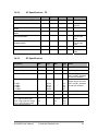
1. Document Control
Created By
Engineering Review
Marketing Review
Approved - Engineering
Approved - Marketing
Tom Marks
Revision
1.0.1
1.5.0
Author
TRM
TRM
Date
12/9/2003
3/12/2005
1.6
TRM
1/22/2007
12/15/04
Description
Document Created, Preliminary
Document modified to match initial release. Channel
tables changed substantially to match regulatory
requirements
Various document corrections and clarifications
- ii –
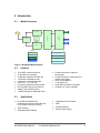
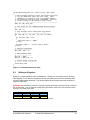
2. Introduction
Module Overview
TRANSMITTER
BASEBAND DSP
ANTENNA SWITCH
COMBINER
UART
CONTROL
ANTENNA
VCO
PROTOCOL
CONTROLLER
2.1.
ANALOG IN
DIGITAL I/O
DATA
RECEIVER
LEGEND
HARDWARE IN WISE
Wi.232 APPLICATION
SOFTWARE IN WISE
WiSE MAC
SERIAL INTERFACE
WiSE PACKET
I/O INTERFACE
HAL
Figure 1: Wi.232EUR Block Diagram
2.2.
•
•
•
•
•
•
•
•
•
•
True UART to antenna solution
16-bit CRC error checking
76.8kbit/sec maximum RF data rate
2 channels in Wideband mode
6 channels in Narrowband mode
Small size – .8” x .935” .08”
Low power standby and sleep modes
PHY and MAC layer protocol built in
CSMA medium access control
115dB link budget in Wideband mode
2.3.
•
Features
•
•
•
•
•
•
8 modes allow user to optimize
power/range
Command mode for volatile and nonvolatile configuration
48-bit unique address
5 volt tolerant I/O
Under $20 in production quantities
915MHz U.S. version available
Applications
Direct RS-232/422/485 wire
replacement (requires external RS-232
to 3V CMOS conversion circuitry)
•
Industrial/Home Automation
•
RFID
•
Asset Tracking
•
Wireless Sensors
•
Automated Meter Reading
•
Remote Data Logging
Wi.232EUR User’s Manual
© 2003-2007 Radiotronix Inc.
2
3. Table of Contents
1.
2.
Document Control ...............................................................................................................2
Introduction..........................................................................................................................2
2.1. Module Overview .............................................................................................................. 2
2.2. Features ............................................................................................................................ 2
2.3. Applications....................................................................................................................... 2
3.
Table of Contents ................................................................................................................3
4.
Table of Figures ...................................................................................................................4
5.
Index of Tables.....................................................................................................................4
6.
Theory of Operation ............................................................................................................5
6.1. General.............................................................................................................................. 5
6.2. Operating States ............................................................................................................... 8
6.3. Resetting Module to Factory Defaults............................................................................... 9
7.
Application Information ....................................................................................................10
7.1. Pin-out Diagram .............................................................................................................. 10
7.2. Pin Description ................................................................................................................ 10
7.3. Mechanical Drawings ...................................................................................................... 11
7.4. Example Circuit ............................................................................................................... 13
7.5. Power Supply .................................................................................................................. 13
7.6. UART Interface ............................................................................................................... 13
7.7. Antenna ........................................................................................................................... 14
7.8. Link budget, transmit power, and range performance .................................................... 14
8.
Module Configuration........................................................................................................15
8.1. Channel settings ............................................................................................................. 15
8.2. Power Mode .................................................................................................................... 16
8.2.1. Wideband Mode....................................................................................................... 16
8.2.2. Narrowband Mode ................................................................................................... 17
8.3. UART Data Rate ............................................................................................................. 17
8.4. Network Mode ................................................................................................................. 18
8.5. Transmit Wait Timeout .................................................................................................... 18
8.6. Network Group ................................................................................................................ 18
8.7. CRC Control.................................................................................................................... 18
8.8. UART minimum transmission unit................................................................................... 19
8.9. Verbose mode................................................................................................................. 19
8.10.
CSMA enable .............................................................................................................. 19
8.11.
Sleep control................................................................................................................ 19
8.12.
MAC Address .............................................................................................................. 20
8.13.
Register Summary....................................................................................................... 21
9.
Using Configuration Registers.........................................................................................21
9.1. CMD Pin .......................................................................................................................... 21
9.2. Command Formatting ..................................................................................................... 22
9.3. Writing To Registers........................................................................................................ 23
9.4. Reading From Registers ................................................................................................. 24
10.
Electrical Specifications ...................................................................................................25
10.1.
Absolute Maximum Ratings......................................................................................... 25
10.2.
Detailed Electrical Specifications ................................................................................ 25
10.2.1.
AC Specifications – RX ........................................................................................ 25
10.2.2.
AC Specifications – TX ........................................................................................ 26
10.2.3.
DC Specifications ................................................................................................. 26
10.3.
Flash Specifications (Non-Volatile Registers) ............................................................. 27
11.
Custom Applications.........................................................................................................28
12.
Ordering Information.........................................................................................................28
13.
Contact Us..........................................................................................................................28
13.1.
Technical Support........................................................................................................ 28
13.2.
Sales Support .............................................................................................................. 28
Wi.232EUR User’s Manual
© 2003-2007 Radiotronix Inc.
3
4. Table of Figures
Figure 1: Wi.232EUR Block Diagram .............................................................................................. 2
Figure 2: WiSE Block Diagram ........................................................................................................ 5
Figure 3: Wi.232EUR Networking Concept ..................................................................................... 6
Figure 4: RX State Machine ............................................................................................................ 8
Figure 5: TX State Machine............................................................................................................. 9
Figure 7: Pin-out diagram .............................................................................................................. 10
Figure 8: Module Mechanical Drawings ........................................................................................ 11
Figure 9: Wi.232EUR/Wi.232DTS Suggested Footprint ............................................................... 12
Figure 10: Evaluation Module Circuit............................................................................................. 13
Figure 11: Command and CMD Pin Timing .................................................................................. 22
Figure 12: Command Conversion Code........................................................................................ 23
5. Index of Tables
Table 1, Module Pin Descriptions.................................................................................................. 10
Table 2, Wi.232EUR UART Interface Lines .................................................................................. 14
Table 3, Channel Table ................................................................................................................. 16
Table 4, Power Mode Register Settings........................................................................................ 16
Table 5, Wideband Mode Parameters........................................................................................... 17
Table 6, narrowband Mode Parameters........................................................................................ 17
Table 7, Data Rate Register Settings............................................................................................ 17
Table 8, Register Summary........................................................................................................... 21
Table 9, Write Register Command, value to be written is less than 128 (0x80). .......................... 23
Table 10, Write Register Command, value to be written is greater than or equal to 128 (0x80). . 24
Table 11, Read Register Command .............................................................................................. 24
Table 12, Read Register Module Response For A Valid Register ................................................ 24
Table 13, Absolute Maximum Ratings........................................................................................... 25
Table 14, AC Specifications - Rx................................................................................................... 25
Table 15, AC Specifications - Tx ................................................................................................... 26
Table 16, DC Specifications .......................................................................................................... 26
Table 17, Flash Specifications (Non-Volatile Registers) ............................................................... 27
Wi.232EUR User’s Manual
© 2003-2007 Radiotronix Inc.
4
6. Theory of Operation
6.1.
General
The Wi.232 module is one of a family of WiSE™ (Wireless Serial Engine) modules. A WiSE™
module combines a state-of-the-art wideband/FSK data transceiver and a high-performance
protocol controller to create a complete embedded wireless communications link in a tiny IC-style
package.
Figure 2: WiSE Block Diagram
The Wi.232EUR module has a UART-type serial interface and contains special application
software to create a transparent UART-to-antenna wireless solution capable of direct wire
replacement in most embedded RS-232/422/485 applications.
NOTE: Although the module is capable of supporting the typical serial communications required
by RS-232, RS-422, and RS-485 networks, it is not compatible with the electrical interfaces for
these types of networks. The module has CMOS inputs and outputs and would require an
appropriate converter for the particular type of network it is connected to.
Wi.232EUR User’s Manual
© 2003-2007 Radiotronix Inc.
5
Figure 3: Wi.232EUR Networking Concept
The module is designed to interface directly to a host UART. Three signals are used to transfer
data between the module and the host UART: TXD, RXD, and CTS. TXD is the data output from
the module RXD is the data input to the module. CTS is an output that indicates the status of the
module’s data interface. If CTS is low, the module is ready to accept data. If CTS is high, the
module is busy and the host UART should not send any further data.
Internally, the module has a 192 byte buffer for incoming characters from the host UART. The
module can be programmed to automatically transmit when the buffer reaches a programmed
limit, set by regUARTMTU. The module can also be programmed to transmit based on
a delay between characters, set by regTXTO(set in 1mSec increments). These registers allow
the designer to optimize performance of the module for fixed length and variable length data. The
module will support streaming data, as well. To optimize the module for streaming data,
regUARTMTU should be set to 144, and regTXTO should be set to a value equal to 1 byte time
at the current UART data rate or 2, whichever is greater. If the buffer is full, or the timer set by
regTXTO expires, and the module is in the process of sending the previous packet over the RF
link, the module will assert CTS high, indicating that the host should not send any more data.
Data sent by the host while CTS is high will be lost.
When the MAC layer has a packet to send, it will use a carrier-sense-multiple-access (CSMA)
protocol to determine if another module is already transmitting. If another module is transmitting,
the module will receive that data before attempting to transmit its data again. If, during this
process, the UART receive buffer gets full, the CTS line will go high to prevent the host UART
from over-running the receive buffer. The CSMA mechanism introduces a variable delay to the
transmission channel. This delay is the sum of a random period and a weighted period that is
dependent on the number of times that the module has tried and failed to acquire the channel.
For applications that guarantee that only one module will be transmitting at any given time, the
CSMA mechanism can be turned off to avoid this delay.
The MAC layer prefixes the data with a packet header and postfixes the data with a 16-bit CRC.
The 16-bit CRC error checking can be disabled to allow the application to do its own error
checking. Data is encoded using a proprietary algorithm (DirectSPREAD™) to spread the RF
energy equally within the transmission bandwidth.
Wi.232EUR User’s Manual
© 2003-2007 Radiotronix Inc.
6
Modules can operate in groups. Each module can be assigned a 7-bit group ID, which is used to
logically link it to other modules on the same channel. All modules on a channel will interoperate,
regardless of their respective group Ids. In other words, the CSMA mechanism will prevent
collisions of modules on the same channel but belonging to different groups.
Modules can also operate in two network modes: Master/Slave and Peer-to-Peer. These modes
define a set of communication rules that identifies which modules can talk to any given module.
In Master/Slave mode, masters can talk to slaves and other masters, slaves can talk to masters,
but slaves cannot talk to other slaves. This mode is sometimes required for applications that are
replacing legacy RS-485 networks. In peer-to-peer mode, any module can hear any other
module. In both modes, group integrity is enforced.
When a module transmits a packet, all other modules on the same channel will receive the
packet, check the packet for errors, and determine whether the received group ID matches the
local group ID. If the packet is error free and the group Ids match, the module will decrypt the
data if necessary, and send the error free data to its host UART for processing. The modules
only implement the ISO reference network stack up to the MAC layer, so they are transparent to
link layer addressing schemes. Therefore, the modules can work with any link-layer and higher
protocols in existing today.
Certain features of the module are controlled through programmable registers. Registers are
access by bringing CMD low. When CMD is low, all data transfers from the host UART are
considered to be register access commands. When CMD is high, all data transfers from the host
UART are considered to be raw data that needs to be transparently transmitted across the
wireless link. The module maintains two copies of each register: one in flash and one in RAM.
On reset, the module loads the RAM registers from the values in the flash registers. The module
is operated out of the RAM registers. Applications that need to change parameters of the module
often would simply modify the RAM register. By putting default settings in the flash registers, the
module will always come up in a preconfigured state, which is useful for applications that do not
have external microcontrollers, such as RS-232 adapters.
The UART interface is capable of operating in full duplex at baud rates from 2.4 to 115.2 kbps.
The module has 10 power modes: 4 wideband modes, 4 narrowband modes, standby, and sleep.
In wideband mode, the module’s channel bandwidth is set to 600kHz. In this mode, the module
can operate on 2 channels and support a maximum RF data rate of 76.8kbit/second. The
receiver sensitivity at the max data rate is –102dBm typical, yielding a maximum link budget of
115dB. This mode is an excellent alternative to frequency hopping spread spectrum. It requires
no synchronization, allowing it to operate in a duty-cycle mode for extended battery life.
In narrowband mode, the module’s channel bandwidth is set to 200kHz. In this mode, the module
can operate on 6 channels and supports a maximum data rate of 9600 baud. The receiver
sensitivity at the maximum data rate is –104 typical, yielding a link budget of 117dB.
The module can be placed into sleep mode through the command mode. In sleep mode, the RF
section is completely shutdown, and the protocol processor is in an idle state. Once the module
has been placed in the sleep mode, it can be awakened by either cycling power, which will loose
all volatile settings, or by sending a power-up sequence through the serial port. The power up
sequence is 0x00, 0xFF, 0xFF, 0xFF sent back-to-back at the data rate for which the module is
configured.
Note: When in sleep mode, the module will not be able to receive data from other modules. Any
data sent to the module while it is in sleep mode will be lost.
Wi.232EUR User’s Manual
© 2003-2007 Radiotronix Inc.
7
If the current draw in sleep mode is too high for a particular application, the designer can switch
power to the module through a switching transistor to “turn-off” the module when it is not needed.
If this technique is used, the volatile registers will reset to the values in their non-volatile mirrors,
so any changes from the default will have to be reloaded.
The Wi.232EUR is a very flexible module because of all of the configurable parameters it
supports. However, modules that are not configured in the same way will not be able to
communicate reliably, causing poor performance or outright failure of the wireless link. All
modules in a network must have the same mode configuration to ensure interoperability.
Every Wi.232 module has read-only internal registers that contain factory programmed
information that includes calibration data and a 48-bit MAC address that can be used by the host
application for higher level, connection oriented protocols. This MAC address can be read
through the command interface.
6.2.
Operating States
The primary active state is the IDLE state. When the module is not actively transmitting or
receiving data, it is in this state. While in this state, the receiver is enabled and the module is
continuously listening for incoming data. If the module detects a pre-amble and valid start-code,
it will enter the RX_HEADER state.
IS R
RF
E O U T
R X T IM
R X H E A D E R
HE
R X D A T A
AD
ER
ID L E M O D E
OK
D A T A LE N <M T U
RX
DO
NE
CR
P
B
C-
K
AC
AD
ET
Q
UE
D
RFIS
R
C R C
U A R T T X
Figure 4: RX State Machine
If the module is in the IDLE state and a byte is received by the UART, it will enter the TX_WAIT
state.
Wi.232EUR User’s Manual
© 2003-2007 Radiotronix Inc.
8
RX HEADER
RF
TU
=M
EN
L
UT
R
TA O EO
DA
IM
T
TX
X
TR
UAR
IS
R
IDLE MODE
DATALEN<MTU
TX WAIT
TE
PLE
COM
TX
CSMA
Figure 5: TX State Machine
6.3.
Resetting Module to Factory Defaults
It may be necessary to reset the non-volatile registers to their factory defaults. To reset the
module to factory defaults, hold the command line low and cycle power to the module. The
command line must remain low for a minimum of 600ms after the resetting the module. Once the
command line is released, the module will be operating at factory defaults.
Wi.232EUR User’s Manual
© 2003-2007 Radiotronix Inc.
9
7. Application Information
7.1.
Pin-out Diagram
Figure 6: Pin-out diagram
7.2.
No.
1
2
3
4
5
6
7
8
9
10
11
12
13
14
15
16
17
18
19
Pin Description
Description
Ground
No connect – reserved
No connect – reserved
Command input – active low
UART receive input
UART transmit output
UART clear to send output – active
low
No connect – reserved
No connect – reserved
Reserved – ISP pin
Active-low Reset / Reserved – ISP pin
Ground
Antenna port – 50 ohm
Ground
Ground
Ground
Ground
Ground
VCC – 2.7 to 3.6 VDC
Table 1, Module Pin Descriptions
Legend
Signals that are used in this implementation
Signals not used in this implementation –do not connect
Signals used for in-system programming
Wi.232EUR User’s Manual
© 2003-2007 Radiotronix Inc.
10
7.3.
Mechanical Drawings
Figure 7: Module Mechanical Drawings
Wi.232EUR User’s Manual
© 2003-2007 Radiotronix Inc.
11
Figure 8: Wi.232EUR/Wi.232DTS Suggested Footprint
Wi.232EUR User’s Manual
© 2003-2007 Radiotronix Inc.
12
7.4.
Example Circuit
Figure 9: Evaluation Module Circuit
7.5.
Power Supply
Although the Wi.232EUR module is very easy to use, care must be given to the design of the
power supply circuit. It is important for the power supply to be free of digital noise generated by
other parts of the application circuit, such as the RS-232 converter.
Figure 4 shows the schematic for our evaluation module circuit for the Wi.232EUR module. It
includes an on-board power supply and antenna connector. This evaluation circuit was used to
measure the performance of the Wi.232EUR module.
If noise is a problem, it can usually be eliminated by adding bypass capacitance or inductive
choking to the power supply, using a dedicated LDO regulator for the module, and/or by
separating the grounds for the module and the other circuits.
7.6.
UART Interface
The UART interface is very simple; it is comprised of four CMOS compatible digital lines.
Wi.232EUR User’s Manual
© 2003-2007 Radiotronix Inc.
13
Line
Direction
Description
CTS
Out
Clear to send – this pin indicates to the host micro when it is ok to send data.
When CTS is high, the host micro should stop sending data to the module until
CTS returns to the low state.
CMD
In
Command – the host micro will bring this pin low to put the module in
command mode. Command mode is used to set and read the internal
registers that control the operation of the module. When CMD is high,
the module will transparently transfer data to and from other modules
on the same channel.
RXD
TXD
In
Out
NOTE: If this pin is low when the module comes out of reset, the registers will
be reset to their factory programmed defaults. It is important to ensure that
CMD is held high during power-up under normal conditions.
Receive data input.
Transmit data output
Table 2, Wi.232EUR UART Interface Lines
7.7.
Antenna
The module is designed to work with any 50-ohm antenna, including PCB trace antennas.
We are often asked: “What is the best antenna to use with your module?” Actually, the selection
of an antenna is based on a particular application, not the module used.
As a rule, either a ¼ wave whip or ½ wave dipole antenna paired with a good, solid ground plane
are good choices. However, many embedded applications cannot support an externally mounted
antenna. If this is the case, a PCB antenna must be used. The designer can either use an off-ofthe-shelf PCB antenna, or design a trace antenna.
Note: Antenna design is difficult and can be impossible without the proper test equipment. As
such, we strongly encourage all of our customers to use off-of-the-shelf antennas whenever
possible.
7.8.
Link budget, transmit power, and range performance
A link budget is the best figure of merit for comparing wireless solutions and determining how
they will perform in the field.
In general, the solution with the best link budget will deliver the best line-of-sight range
performance. Improving the link budget by increasing the receiver sensitivity will result in lower
power consumption while improving the link budget by increasing the transmit power will result in
more robust performance in the presence of an on-channel interferer or multi-path interference.
Wireless Fact: Frequency hopping spread spectrum does not effectively combat multipath
interference in the 868-870 MHz band. It does combat in-channel interference, but at the
expense of bandwidth, power consumption, and latency. Direct sequence spread spectrum, like
FHSS, does not combat multipath interference. It does do a better job than FHSS at combating
in-channel interference, but at the expensive of occupied bandwidth and power consumption.
These spread spectrum techniques are generally chosen because higher output powers are
allowed from a transmitter employing these techniques.
To calculate the link budget for a wireless link, simply add the transmit power, the antenna gains,
and the receiver sensitivity:
LB = Ptx + Gtxa − SENSrx + Grxa
Wi.232EUR User’s Manual
© 2003-2007 Radiotronix Inc.
14
For example, the link budget for a pair of Wi.232 modules in wideband mode at the maximum
data rate and using 2dBi dipole antennas would be:
+13dBm + 2dB – (-102dBm) + 2dB = 119dB
A link budget of 119dB should easily yield a range of ¼ mile or more outdoors. If the environment
is open and the antennas are 8 to 10 feet off of the ground, the range could be a mile. Indoors,
this link budget should yield a range of several hundred feet.
This is a well-balanced link budget. More than 10dB of the budget is achieved through transmit
power, which will allow good performance indoors in the presence of multi-path while keeping the
overall operating current low, making the module suitable for primary battery powered
applications such as RFID and automated meter reading.
8. Module Configuration
8.1.
Channel settings
regNVTXCHAN (0x00)
R/W
R/W
R/W
RES
D6
D5
7
6
5
R/W
D4
4
R/W
D3
3
R/W
D2
2
regTXCHAN (0x4B)
R/W
R/W
D1
D0
1
0
regNVRXCHAN (0x01)
R/W
R/W
R/W
RES
D6
D5
7
6
5
R/W
D4
4
R/W
D3
3
R/W
D2
2
regRXCHAN (0x4C)
R/W
R/W
D1
D0
1
0
The Wi.232EUR supports 2 channels (0 – 1) in wideband mode and 6 channels (0 – 5) in
narrowband mode.
Wi.232EUR User’s Manual
© 2003-2007 Radiotronix Inc.
15
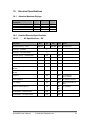
Wideband Channels
Frequency
868.300 MHz
868.95 MHz
Narrowband Channels
Frequency
868.225 MHz
868.375 MHz
868.850 MHz
869.050 MHz
869.525 MHz
869.850 MHz
Channel Number
0
1
Channel Number
0
1
2
3
4
5
Table 3, Channel Table
Transmit and receive channels are set in regTXCHAN (addr 0x4B) and regRXCHAN (addr
0x4C) respectively.
All modules in a network must be in the same mode (narrowband or wideband) and must have
the same transmit and receive channels programmed in order to communicate properly.
8.2.
Power Mode
The transmission and reception modes of the module are determined by the settings of the
regPWRMODE register. It is important to note that a module configured to operate in narrowband
mode cannot “hear” another module transmitting in wideband mode, or vice versa. However, a
module configured to operate in any of the four wideband modes can “hear” any other module
transmitting in any of the wideband modes (provided that they are within range of one another).
regNVPWRMODE (0x02)
R/W
R/W
R/W
NA
NA
NA
7
6
5
PM1
0
0
0
0
1
1
1
1
PM1
0
0
1
1
0
0
1
1
PM0
0
1
0
1
0
1
0
1
R/W
NA
4
R/W
NA
3
regPWRMODE (0x4D)
R/W
R/W
R/W
PM2
PM1
PM0
2
1
0
Mode
Narrowband Mode – -2dBm power setting (typical)
Wideband Mode – +2dBm power setting (typical)
Wideband Mode – +7dBm power setting (typical)
Wideband Mode – +13dBm power setting (typical)
Wideband Mode – -2dBm power setting (typical)
Narrowband Mode – +2dBm power setting (typical)
Narrowband Mode – +7dBm power setting (typical)
Narrowband Mode – +13dBm power setting (typical)
Table 4, Power Mode Register Settings
8.2.1. Wideband Mode
In wideband mode, the module is configured as follows:
Wi.232EUR User’s Manual
© 2003-2007 Radiotronix Inc.
16
wideband Mode Parameters
TX Power
-2, +2, +7, +13 dBm
Deviation
+/-80kHz
TX Current
26 to 65mA
RX Current
16 to 20mA
RX Bandwidth
600kHz
Table 5, Wideband Mode Parameters
8.2.2. Narrowband Mode
In low-power mode, the module is configured as follows:
narrowband Mode Parameters
TX Power
-2, +2, +7, +13 dBm
Deviation
+/-40kHz
TX Current
26 to 65mA
RX Current
16 to 24mA
RX Bandwidth
200kHz
Table 6, Narrowband Mode Parameters
8.3.
UART Data Rate
regNVDATARATE (0x03)
R/W
R/W
R/W
RES
RES
RES
7
6
5
R/W
RES
4
R/W
RES
3
regDATARATE (0x4E)
R/W
R/W
R/W
BR2
BR1
BR0
2
1
0
By default, the UART data rate is set to 2.4 kbit/second at the factory. This data rate can be
changed by setting the regDATARATE register. The data rate should be limited to 9600 bits/sec
when in narrowband mode. Exceeding this rate will result in poor link quality. Valid settings are:
Baud Rate
2400
9600
19200
38400
57600
115200
10400
31250
BR2
0
0
0
0
1
1
1
1
BR1
0
0
1
1
0
0
1
1
BR0
0
1
0
1
0
1
0
1
Table 7, Data Rate Register Settings
TROUBLESHOOTING HINT: Baud Rate Problems. If you lose track of the baud rate setting of
the module, it will be impossible to program the module. You can either try every possible baud
rate to discover the setting, or force a power-on reset with CMD held low to set the baud rate to
its default: 2.4kbit/second.
Wi.232EUR User’s Manual
© 2003-2007 Radiotronix Inc.
17
8.4.
Network Mode
regNVNETMODE (0x04)
R/W
R/W
R/W
D7
D6
D5
7
6
5
R/W
D4
4
R/W
D3
3
regNETMODE (0x4F)
R/W
R/W
R/W
D2
D1
D0
2
1
0
The module supports two networking modes: Normal and Slave.
In normal mode, the module can talk to any other module. In slave mode, the module can talk to
normal-mode modules, but cannot transmit to or receive from other slaves.
Slave mode is selected by writing 0x00 to this register. The default network mode is 0x01
(Normal Mode).
8.5.
R/W
D7
7
Transmit Wait Timeout
regNVTXTO (0x05)
R/W
R/W
D6
D5
6
5
R/W
D4
4
R/W
D3
3
R/W
D2
2
regTXTO (0x50)
R/W
R/W
D1
D0
1
0
When a byte is received by the UART, the module will start a timer that will countdown every
millisecond. The timer is restarted when each byte is received.
If the timer reaches zero before the next byte is received from the UART, the module begin
transmitting the data in the buffer. Normally, this timeout value should be greater than 0x01 and
greater than one byte time at the current UART data rate. If the timeout value is set to 0x00, the
transmit wait timeout will not operate, and a full buffer will be required for transmission. When
configured this way, the data will be sent only when a full MTU has been received through the
UART. The default setting for this register is 0x10 (~16ms delay).
8.6.
Network Group
regNVNETGRP (0x06)
R/W
R/W
R/W
N/A
B6
B5
7
6
5
R/W
B4
4
R/W
B3
3
R/W
B2
2
regNETGRP (0x51)
R/W
R/W
B1
B0
1
0
Modules can be grouped into networks. Although only modules with the group ID will be able to
talk to each other, modules in different groups but on the same channel will still coordinate
transmissions through the CSMA mechanism. Valid values for this register are 0 to 127. The
default group setting is 0.
8.7.
CRC Control
regNVUSECRC (0x08)
R/W
R/W
R/W
B7
B6
B5
7
6
5
Wi.232EUR User’s Manual
R/W
B4
4
R/W
B3
3
© 2003-2007 Radiotronix Inc.
R/W
B2
2
regUSECRC (0x53)
R/W
R/W
B1
B0
1
0
18
Set to 0x01 to enable CRC mode, or 0x00 to disable CRC mode. The default CRC mode setting
is enabled.
8.8.
UART minimum transmission unit
regNVUARTMTU (0x09)
R/W
R/W
R/W
B7
B6
B5
7
6
5
R/W
B4
4
R/W
B3
3
regUARTMTU (0x54)
R/W
R/W
R/W
B2
B1
B0
2
1
0
This register determines the UART buffer level that will trigger the transmission of a packet. The
minimum value is 1 and the maximum value is 144. The default value for this register is 64,
which provides a good mix of throughput and latency.
8.9.
Verbose mode
regNVSHOWVER (0x0A)
R/W
R/W
R/W
B7
B6
B5
7
6
5
R/W
B4
4
R/W
B3
3
R/W
B2
2
R/W
B1
1
R/W
B0
0
Setting this register to 0x00 will suppress the start-up message, including firmware version, that is
sent to the UART when the module is reset. A value of 0x01 will cause the message to be
displayed after reset. By default, the module start-up message will be displayed.
8.10. CSMA enable
regNVCSMAMODE (0x0B)
R/W
R/W
R/W
B7
B6
B5
7
6
5
R/W
B4
4
R/W
B3
3
regCSMAMODE (0x56)
R/W
R/W
R/W
B2
B1
B0
2
1
0
Carrier-sense multiple access (CSMA) is a best-effort delivery system that listens to the channel
before transmitting a message. If another Wi.232 module is already transmitting when a
message is queued, the module will wait before sending its payload. This helps to eliminate RF
message corruption at the expense of additional latency. Setting this register to 0x01 will enable
CSMA. Setting this register to 0x00 will disable CSMA. By default, CSMA is enabled.
8.11. Sleep control
regNVSLPMODE (0x0D)
R/W
R/W
R/W
B7
B6
B5
7
6
5
R/W
B4
4
R/W
B3
3
regSLPMODE (0x58)
R/W
R/W
R/W
B2
B1
B0
2
1
0
Setting this register to 0x01 will place the module into sleep mode; 0x02 will place the module in
standby mode. Sleep mode places the module in the lowest power inactive state (~35µA) and
requires approximately 7-8ms to resume transmission or reception once awakened. Standby
draws ~850µA and requires approximately 1-2ms to awaken. To wake up the module, send four
0xFF bytes to the UART in a row or perform a hard reset. If four 0xFF bytes are used to wake the
module, the fifth character sent to the UART will be transmitted over the RF link. Upon
Wi.232EUR User’s Manual
© 2003-2007 Radiotronix Inc.
19
awakening, the module will clear the volatile register to 0x00. The default value for this register is
0x00 (awake).
8.12. MAC Address
regOUI2 – regOUI0 (0x22 – 0x24)
R
R
R
D7
D6
D5
7
6
5
R
D4
4
R
D3
3
R
D2
2
N/A
R
D1
1
R
D0
0
regMAC2 – regMAC0 (0x25 – 0x27)
R/W
R/W
R/W
RES
D6
D5
7
6
5
R/W
D4
4
R/W
D3
3
R/W
D2
2
N/A
R/W
D1
1
R/W
D0
0
These registers make a unique 48-bit MAC address. These values are factory preset and cannot
be altered. These address bytes are not used by the module. They are provided for customer
applications as a unique address.
Wi.232EUR User’s Manual
© 2003-2007 Radiotronix Inc.
20
8.13. Register Summary
Name
regTXCHANNEL
regRXCHANNEL
regPWRMODE
regDATARATE
regNETMODE
regTXTO
regNETGRP
regUSECRC
regUARTMTU
Reserved
regCSMAMODE
regSLPMODE
Name
regMAC0
regMAC1
regMAC2
regOUI0
regOUI1
regOUI2
Name
regNVTXCHANNEL
regNVRXCHANNEL
regNVPWRMODE
regNVDATARATE
regNVNETMODE
regNVTXTO
regNVNETGRP
regNVUSECRC
regNVUARTMTU
regNVSHOWVER
regNVCSMAMODE
regNVSLPMODE
Volatile Read/Write Registers
Address
Description
0x4B
Transmit channel setting
0x4C
Receive channel setting
0x4D
Operating mode settings
0x4E
UART data rate
0x4F
Network mode (Normal or Slave)
0x50
Transmit wait timeout
0x51
Network group ID
0x53
Enable/Disable CRC
0x54
Minimum transmission unit.
0x55
0x56
Enable/disable CSMA
0x58
Power state of module
Non-volatile Read Only Registers
Address
Description
0x22
These registers form the unique 48-bit MAC address.
0x23
0x24
0x25
0x26
0x27
Non-volatile Registers
Address
Description
Default
0x00
Transmit channel setting
0
0x01
Receive channel setting
0
0x02
Operating mode settings
+13 dBm wideband
mode
0x03
UART data rate
2400bps
0x04
Network mode (Normal/Slave)
Normal
0x05
Transmit wait timeout
~16ms
0x06
Network group ID
0x00
0x08
Enable/Disable CRC
Enabled
0x09
Minimum transmission unit.
64 bytes
0x0A
Enable/Disable start-up message
Enabled
0x0B
Enable/Disable CSMA
Enabled
0x0D
Power state of module
Awake
Table 8, Register Summary
9. Using Configuration Registers
9.1.
CMD Pin
The CMD pin is used to inform the module where incoming UART information should be routed.
When the CMD pin is high or left floating, all incoming UART information is treated as payload
data and transferred over the wireless interface. If the CMD pin is low, the incoming UART data
is routed to the command parser for processing. Since the module’s processor looks at UART
data one byte at a time, the CMD line must be held low for the entire duration of the command
plus a 20µs margin for processing. Leaving the CMD pin low for additional time (for example,
until the ACK byte is received by your application) will not adversely affect the module. If RF
Wi.232EUR User’s Manual
© 2003-2007 Radiotronix Inc.
21
packets are received while the CMD line is active, they are still processed and presented to the
module’s UART for transmission.
Figure 10: Command and CMD Pin Timing
9.2.
Command Formatting
The Wi.232EUR module contains several volatile and non-volatile registers that control its
configuration and operation. The volatile registers all have a non-volatile mirror register that is
used to determine the default configuration when power is applied to the module. During normal
operation, the volatile registers are used to control the module.
Placing the module in the command mode allows these registers to be programmed. Byte values
in excess of 127 (0x80 or greater) must be changed into a two-byte escape sequence of the
format: 0xFE, [value - 128]. For example, the value 0x83 becomes 0xFE, 0x03. The following
function will prefix a 0xFF header and size specifier to a command sequence and create escape
sequences as needed. It is assumed that *src is populated with either the register number to
read (one byte, pass 1 into src_len) or the register number and value to write (two bytes, pass
2 into src_len). It is also assumed that the *dest buffer has enough space for the two header
characters plus, the encoded command, and the null terminator.
Wi.232EUR User’s Manual
© 2003-2007 Radiotronix Inc.
22
int EscapeString(char *src, char src_len, char *dest)
{
// The following function copies and encodes the first
// src_len characters from *src into *dest. This
// encoding is necessary for Wi.232 command formats.
// The resulting string is null terminated. The size
// of this string is the function return value.
// --------------------------------------------------char src_idx, dest_idx;
// Save space for the command header and size bytes
// -----------------------------------------------dest_idx = 2;
// Loop through source string and copy/encode
// -----------------------------------------for (src_idx = 0; src_idx < src_len; src_idx++)
{
if (src[src_idx] > 127)
{
dest[dest_idx++] = 0xFE;
}/*if*/
dest[dest_idx++] = (src[src_idx] & 0x7F);
}/*for*/
// Add null terminator
// ------------------dest[dest_idx] = 0;
// Add command header
// -----------------dest[0] = 0xFF;
dest[1] = dest_idx – 2;
// Return escape string size
// ------------------------return dest_idx;
}
Figure 11: Command Conversion Code
9.3.
Writing to Registers
Writing to a volatile register is nearly instantaneous. Writing to a non-volatile register, however,
takes typically 16 ms. Because the packet size can vary based on the need for encoding, there
are two possible packet structures. The following tables show the byte sequences for writing a
register in each case.
WARNING: Be sure that the module is properly powered and remains powered for the duration of
the register write. Loss of important configuration information could occur if the unit loses power
during a non-volatile write cycle.
Byte 0
Byte 1
Byte 2
Byte 3
Header
Size
Register
Value
7 6 5 4 3 2 1 0 7 6 5 4 3 2 1 0 7 6 5 4 3 2 1 0 7 6 5 4 3 2 1 0
0xFF
0x02
0 Register 0
Value
Table 9, Write Register Command, value to be written is less than 128 (0x80).
Wi.232EUR User’s Manual
© 2003-2007 Radiotronix Inc.
23
Byte 0
Byte 1
Byte 2
Byte 3
Byte 4
Header
Size
Register
Escape
Value
7 6 5 4 3 2 1 0 7 6 5 4 3 2 1 0 7 6 5 4 3 2 1 0 7 6 5 4 3 2 1 0 7 6 5 4 3 2 1 0
Lower 7 bits
of Value
Table 10, Write Register Command, value to be written is greater than or equal to 128 (0x80).
0xFF
0x03
0
Register
0xFE
0
The module will respond to this command with an ACK (0x06). If an ACK is not received, the
command should be resent. If a write is attempted to a read-only or invalid register, the module
will respond with a NAK (0x15).
9.4.
Reading from Registers
A register read command is constructed by placing an escape character before the register
number. The following table shows the byte sequence for reading a register.
Byte 0
Byte 1
Byte 2
Byte 3
Header
Size
Escape
Register
7 6 5 4 3 2 1 0 7 6 5 4 3 2 1 0 7 6 5 4 3 2 1 0 7 6 5 4 3 2 1 0
0xFF
0x02
Table 11, Read Register Command
0xFE
0
Register
The module will respond to this command by sending an ACK (0x06) followed by the register
number and register value. The register value is sent unmodified. For example, if the register
value is 0x83, 0x83 is returned after the ACK (0x06). See table below for the format of the
response. If the register number is invalid, it will respond with a NACK (0x15).
Byte 0
Byte 1
Byte 2
ACK
Register
Value
7 6 5 4 3 2 1 0 7 6 5 4 3 2 1 0 7 6 5 4 3 2 1 0
0x06
0 Register
Value
Table 12, Read Register Module Response for a Valid Register
Wi.232EUR User’s Manual
© 2003-2007 Radiotronix Inc.
24
10.
Electrical Specifications
10.1. Absolute Maximum Ratings
Parameter
VCC – Power Supply
Voltage on any digital I/O pin
Input RF Level
Storage Temperature
Min
Max
Units
2.7
-0.3
3.6
5
15
85
VDC
VDC
dBm
°C
-40
Table 13, Absolute Maximum Ratings
10.2. Detailed Electrical Specifications
10.2.1.
AC Specifications – RX
Parameter
Min
Receive frequency – EUR
Typ
868.225
Channels – wideband
2
Channels – narrowband Mode
6
Channel spacing – wideband Mode
Max
Units
Notes
869.885
MHz
At antenna pin
650
kHz
Channel spacing – narrowband Mode
Variable
kHz
Receiver sensitivity – wideband MODE
-102
dBm
115200 baud UART
Receiver sensitivity – wideband MODE
-106
dBm
2400 baud UART
Receiver sensitivity – narrowband
MODE
-104
dBm
9600 baud UART
Receiver sensitivity – narrowband
MODE
-107
dBm
2400 baud UART
Input IP3
-40
dBm
Flo+1MHz and
Flo+1.945MHz
Input Impedance
50
Ohms
No matching required
LO Leakage
-65
dBm
50-ohm termination at
ANT
Adjacent channel rejection
-48
dBc
Fc +/-650kHz
dBc
IF Bandwidth – wideband Mode
600
KHz
IF Bandwidth – narrowband Mode
200
KHz
Table 14, AC Specifications - Rx
Wi.232EUR User’s Manual
© 2003-2007 Radiotronix Inc.
25
10.2.2.
AC Specifications – TX
Parameter
Min
Typ
Transmit Frequency –EUR
868.225
Max
Units
869.885
MHz
3
ppm
Center frequency error
2
Frequency Deviation – wideband
Mode
Frequency Deviation – narrowband
Mode
Maximum Output Power –
narrowband Mode
+/-80
kHz
+/-40
kHz
13
15
dBm
Maximum Output Power –
wideband Mode
13
15
dBm
Output Impedance
50
Ohms
Harmonic Output
-50
dBc
Notes
869.05 MHz
@ 25°C
869.05 MHz
Into 50 ohm
load
869.05 MHz
Into 50 ohm
load
Into 50 ohm
load
Table 15, AC Specifications - Tx
10.2.3.
DC Specifications
Parameter
Min
Operating Temperature
-40
Supply voltage
2.7
Notes
+85
Unit
s
°C
3.6
VDC
Operating limits
16-24
mA
Continuous operation,
Vdd = 3.3VDC, depends
on data rate selected
-2 dBm
+2 dBm
+7 dBm
+13 dBm
Standby current consumption
24-32
28-36
35-43
50-58
850
mA
mA
mA
mA
µA
Sleep current consumption
35
µA
Receive current consumption
Typ.
3.0
Max
Transmit current consumption
Vih – Logic high level input
Vil – Logic low level input
Voh – Logic high level output
Vol – Logic low level output
0.7*Vcc
0
2.5
0
5
0.3*Vcc
Vcc
.4
Output into 50 ohm load,
Vdd = 3.3VDC, depends
on data rate selected
Vdd = 3.3VDC
Vdd = 3.3VDC
VDC
VDC
VDC
VDC
Table 16, DC Specifications
Wi.232EUR User’s Manual
© 2003-2007 Radiotronix Inc.
26
10.3. Flash Specifications (Non-Volatile Registers)
Parameter
Flash Write Duration
Min
Typ.
16
Flash Write Cycles
20k
100k
Max
21
Units
ms
Notes
Module stalled during
write operation
Cycles
Table 17, Flash Specifications (Non-Volatile Registers)
Wi.232EUR User’s Manual
© 2003-2007 Radiotronix Inc.
27
11.
Custom Applications
For cost-sensitive applications, such as wireless sensors and AMR, Radiotronix can embed the
application software directly into the microcontroller built into the module. For more information
on this service, please contact Radiotronix.
12.
Ordering Information
Wi.232EUR modules can be ordered on-line 24/7 from our distributors: Please visit the following web link to
obtain a list of representatives and distributors who service your region.
http://www.radiotronix.com/corpsales.asp
13.
Contact Us
13.1. Technical Support
Radiotronix has built a solid technical support infrastructure so that you can get answers to your
questions when you need them.
Our primary technical support tools are the support forum and knowledge base found on our
website. We are continuously updating these tools. To find the latest information about these
technical support tools, please visit http://www.radiotronix.com/support/.
TU
UT
Our technical support engineers are available Mon-Fri between 9:30 am and 4:30 pm central
standard time. The best way to reach a technical support engineer is to send an email by visiting
the Support page at http://www.radiotronix.com/support/ . E-mail support requests are given
priority because we can handle them more efficiently that phone support requests.
For customers that would prefer to talk directly to a support engineer, we do offer phone support
free of charge. All support requests are placed in a queue and returned in the order that they are
received.
13.2. Sales Support
Our sales department can be reached via e-mail at [email protected] or by phone at 405794-7730.
TU
UT
Our sales department is available Mon-Fri between 8:30 am and 5:00 pm. You may also contact
our distributors for pre-sales support. Please visit the following website for a list of distributors
and representatives in your area.
http://www.radiotronix.com/corpsales.asp
Wi.232EUR User’s Manual
© 2003-2007 Radiotronix Inc.
28
Mouser Electronics
Authorized Distributor
Click to View Pricing, Inventory, Delivery & Lifecycle Information:
Linx Technologies:
RK-WI.232EUR RK-WI.232EUR-R