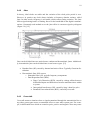
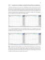
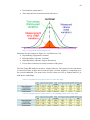
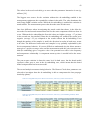
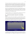
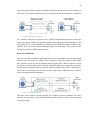
1
JOONAS PUSKALA HIGH-SPEED CAMERA SERIAL INTERFACE VERIFICATION Master of Science Thesis Examiners: Professor Jukka Vanhala Examiner and topic approved in the Electrical Engineering Department Council meeting on 5 November 2014 ii ABSTRACT TAMPERE UNIVERSITY OF TECHNOLOGY Master’s Degree Programme in Signal Processing and Communications Engineering PUSKALA, JOONAS: High-Speed Camera Serial Interface Verification Master of Science Thesis, 51 pages, 0 Appendix pages May 2015 Major: Electronics Product Design Examiner: Professor Jukka Vanhala Keywords: MIPI, D-PHY, multimedia, camera, signal integrity, de-embedding During the last decade, cameras have become a standard part of many personal devices such as mobile phones, personal computers, and tablets. General camera sensor development has been really fast. Picture quality has increased significantly and mobile imaging is getting closer to compact cameras. Technically many camera features such as the resolution, frame rates and application features are improved. This continuous change has an impact for the needed system bandwidth. This thesis focuses on the D-PHY interface verification defined by the international MIPI alliance. The interface is a commonly used standard in the mobile camera and display interface and most of the component suppliers directly support that standard. The current standard revision is the third approved version. When the first standard version supported 1 Gbps per lane, the current version supports lane-speed up to 2.5 Gbps. The increase in bandwidth has brought new needs for the signal integrity verification. During the past years, the camera signal integrity has not been a critical design parameter. Nowadays, the interface performance is often close to its electrophysical limits and many design parameters need to be considered during the system design phase. The purpose of this thesis is to create a reliable verification environment for the D-PHY camera interface verification. The target for quality is to build a reference level measurement environment. The system will replace manual measurements which take a lot of resources. The system will be used in verification, but as important as the verification is to understand better the current and incoming challenges and practical limits in system design. iii TIIVISTELMÄ TAMPEREEN TEKNILLINEN YLIOPISTO Signaalinkäsittely ja tietoliikennetekniikka PUSKALA, JOONAS: High-Speed Camera Serial Interface Verification Diplomityö, 51 sivua, 0 liitesivua Toukokuu 2015 Pääaine: Elektroniikan tuotesuunnittelu Tarkastaja: Professori Jukka Vanhala Avainsanat: MIPI, D-PHY, multimedia, camera, signal integrity, de-embedding Kamerat ovat reilussa kymmenessä vuodessa tulleet kiinteäksi osaksi monia henkilökohtaisia laitteita, kuten matkapuhelimia, tietokoneita ja tabletteja. Samalla kameroiden yleinen kehitys on ollut nopeaa ja tekniset ominaisuudet, kuten kuvanlaatu ovat parantuneet. Samanaikaisesti kuvan resoluutiot ja latenssivaatimukset ovat kasvaneet merkittävästi, mikä on johtanut väylänopeuksien kasvuun. Tässä työssä on keskitytty kansainvälisen MIPI Alliancen määrittelemän D-PHY rajapinnan verifiointiin. Sitä käytetään yleisenä standardina mobiililaitteiden kamera- ja näyttöväylissä. Standardi on kehittynyt viime vuosina merkittävästi ja väylän suurin mahdollinen siirtonopeus on kasvanut ensimmäisen hyväksytyn standardiversion 1 Gbps kaistanleveydestä nykyiseen 2.5 Gbps kaistanleveyteen. Siirtonopeuden kasvu on tuonut uudenlaisen tarpeen kameraväylän verifiointiin ja koko suunnitteluajatteluun. Aiemmin käytetyillä väylänopeuksilla signaalin laatu ei ole ollut kriittinen tekijä tuotesuunnittelussa, kun taas nykyisillä nopeuksilla lähestytään väylänopeuden sähköfysikaalisia rajoja. Tarvittava signaalin laatu voi siten yhtenä keskeisenä tekijänä ohjata jopa koko laitteen suunnittelua. Työn tarkoituksena on ollut luoda kamerasensoreiden D-PHY -rajapinnan verifiointiin luotettava ja helppokäyttöinen ympäristö. Laadullisena tavoitteena on referenssitason mittausjärjestelmä. Se tulee korvaamaan käsin tehtävät mittaukset, jotka vievät hyvin paljon resursseja. Järjestelmää tullaan hyödyntämään kameroiden verifioinnissa, mutta yhtä tärkeää on se, että järjestelmän avulla voidaan ymmärtää paremmin nykyisiä ja tulevaisuuden haasteita komponenttien tuotekehityksessä sekä tuoteintegroinnissa. iv PREFACE I would like to thank M.Sc. Manu Hakola, who was my supervisor at Microsoft. Additionally I want to thank M.Sc. Pentti Väänänen and B.Eng. Jouni Kauhanen, who both supported me in technical and other practical issues during this project. I would also want to thank Professor Jukka Vanhala, who was the examiner of my master’s thesis work. Finally, I want to thank Hanna for helping to proofread the thesis and especially for her endless support in my master’s degree project during the past few years. Tampere 13.5.2015 Joonas Puskala v TABLE OF CONTENTS ABSTRACT ......................................................................................................................ii TIIVISTELMÄ ................................................................................................................iii PREFACE ........................................................................................................................ iv LIST OF SYMBOLS AND ABBREVIATIONS ........................................................... vii 1 INTRODUCTION .................................................................................................... 1 2 MOBILE CAMERA SYSTEM DEVICES ............................................................... 2 2.1 Camera subsystem ............................................................................................. 3 2.2 Electrical camera interfaces .............................................................................. 4 2.3 Camera Serial Interface 2 .................................................................................. 5 2.3.1 D-PHY layer interface ......................................................................... 6 2.3.2 C-PHY layer interface ......................................................................... 8 3 THEORETICAL BACKGROUND ........................................................................ 10 3.1 Transmission line theory ................................................................................. 10 3.1.1 Telegraph equations ........................................................................... 11 3.1.2 Characteristic impedance ................................................................... 12 3.1.3 Signal reflections ............................................................................... 12 3.1.4 Propagation delay .............................................................................. 13 3.2 S-parameters .................................................................................................... 14 3.2.1 Two-port model ................................................................................. 15 3.2.2 Four-port mixed-mode model ............................................................ 15 3.2.3 One-port model .................................................................................. 16 3.3 Differential and single-ended signaling .......................................................... 16 3.4 High-speed signal integrity ............................................................................. 18 3.4.1 Attenuation......................................................................................... 18 3.4.2 Jitter ................................................................................................... 19 3.4.3 Cross-talk ........................................................................................... 19 3.4.4 SKEW ................................................................................................ 20 4 MEASUREMENT SYSTEM ................................................................................. 22 4.1 Verification environment ................................................................................ 22 4.1.1 Camera Add-on-Boards ..................................................................... 23 4.1.2 MIPI camera test board ...................................................................... 24 4.1.3 MIPI D-PHY Reference Termination Board ..................................... 25 4.1.4 Test control unit ................................................................................. 26 4.1.5 Coaxial cables .................................................................................... 27 4.2 Measurement devices ...................................................................................... 27 4.2.1 Required measurement device bandwidth ......................................... 27 4.2.2 Oscilloscope ....................................................................................... 29 4.2.3 Oscilloscope probes ........................................................................... 29 4.2.4 MIPI D-PHY compliance test application software .......................... 31 4.2.5 Test automation.................................................................................. 31 vi 5 CAMERA MODULE SIGNAL INTEGRITY VERIFICATION .......................... 33 5.1 Camera module signal integrity measurement ................................................ 33 5.2 De-embedding ................................................................................................. 34 5.3 Test fixture model creation ............................................................................. 35 5.3.1 Simulations ........................................................................................ 37 5.3.2 S-parameter modelling by using time vector network analyzer ........ 37 5.3.3 S-parameter modelling by using Auto Fixture Removal application 40 6 RESULT ANALYSIS ............................................................................................. 41 6.1 Gauge R&R analysis ....................................................................................... 41 6.2 Normal measurements compared to de-embedding results ............................ 44 6.3 Test fixture design ........................................................................................... 45 6.4 Test system results compared to product verification results ......................... 47 6.5 Alternative test system usage .......................................................................... 48 7 CONCLUSION ....................................................................................................... 50 REFERENCES................................................................................................................ 52 vii LIST OF SYMBOLS AND ABBREVIATIONS A/D AF APS BUJ CCI CCP CMOS CPU CSI DC DCD DDJ DDR DJ DSI DUT EMC FF FPGA Gbps GHz Hi-Res HS I2C IBIS IC IF ISI ISP Low-Res LP Mbps MHz MIPI Mpix PHY PLL RBG RF RJ Analog to Digital Converter Auto Focus Active-Pixel Sensor Bounded Uncorrelated Jitter Camera Control Interface Compact Camera Port Complementary Metal Oxide Semiconductor Central Processing Unit Camera Serial Interface Direct Current Data Cycle Distortion Data Dependent Jitter Double Data Rate Deterministic Jitter Display Serial Interface Device Under Test Electromagnetic Compatibility Fixed-Focus Field-Programmable Gate Array Gigabit Per Second Gigahertz Hi-Resolution High-Speed Inter-Integrated Circuit Input/Output Buffer Information Specification Integrated Circuit Interface Intersymbol Interference Image Signal Processor Low Resolution Low-Power Megabit Per Second Megahertz Mobile Industry Processor Interface Mega Pixel Physical Layer Phase Locked Loop Red Green Blue Radio Frequency Random Jitter viii SI SJ SMIA SoC TDR TLIS UIinst VGA VNA XTAL Signal Integrity Sinusoidal Jitter Standard Mobile Imaging Architecture System-on-Chip Time-Domain Reflectometer Transmission-Line-Interconnect-Structure Unit Interval time. Video Graphics Array Vector Network Analyzer Crystal λ Ω Δz C0 c C D+ / Dp D- / Dn εr f fBW I l L m ρL µr U vp Z0 ω Wave Length Impedance Unit (ohm) Length Unit Speed of Light in Vacuum Characteristic Capacitance per Length Unit Capacitance Positive Differential Line Negative Differential Line Permittivity Frequency Bandwidth Current Characteristic Inductance per Length Unit Inductance Meter Reflection Coefficient Permeability Voltage Phase Velocity Characteristic Impedance Angular Velocity 1 1 INTRODUCTION Nowadays, a high quality digital camera is a standard feature in all smart phones. The history began from the first widely commercial camera phone, which was the Nokia 7650. The phone contains a 0.3Mpix camera sensor with VGA (640x480) resolution. The quality of mobile imaging has taken giant steps during the last couple of years and outstrips traditional digital cameras in many technology areas, like the camera sensor resolution and advanced technologies like the Nokia Pureview. Today, the highest resolution is 41 Mpix, which sets quite different requirements for the data paths and digital imaging processing. Parallel with the resolutions, also frame rates and other feature requirements need more system bandwidth. During the last years, the bandwidth has mainly grown by adding more parallel data-lanes without significant frequency increase. The supported maximum data-lane amount in the specification is reached and a way to increase the bandwidth is to increase the frequency. Higher frequencies bring new challenges for the signal integrity and system design quality. So far, the frequencies used, have not been critical for the system design, but on the other hand, it is known that frequencies are close to their electrophysical limits. The DPHY interface specification states the same: the maximum frequencies and required timings are defined, but at the same time the specification states that the maximum achievable bit rate frequency is dependent on the performance of the transmitter, the interconnection and the receiver design quality. This thesis focuses on the camera serial interface test environment development and signal integrity verification. The used standard is the MIPI D-PHY CSI-2 (Mobile Industry Processor Interface D-Physical Layer Camera Serial Interface 2), which is a commonly used camera serial interface standard in mobile devices. The main objective is to build a high quality and reliable camera module verification environment. The target of the environment is to set the reference quality for the camera serial interface verification. The setup will help to understand better which interface signal integrity factors are critical for the future projects, and what are the practical limits for the interface. 2 2 MOBILE CAMERA SYSTEM DEVICES This chapter gives a short overview of the mobile phone camera sub-system architecture and the used interfaces. Most of the mobile device manufacturers and component suppliers have joined the Mobile Industry Processor Interface (MIPI) alliance. It is an international forum which specifies the general standards commonly used in mobile devices, ranging from smartphones to wireless-enabled devices and netbooks. The standards specified by the MIPI Alliance may impact both hardware and software. The main purpose is to create general standards which are freely available for all the alliance members. The common standards guarantee that the components and chipsets are compatible with each other and the same components can be used in different platforms. [1] Standard Mobile Imaging Architecture (SMIA) was originally Nokia Corporation’s, nowadays Microsoft Corporation’s, standard for mobile cameras. The standard generations are SMIA and SMIA++, which is an upgrade from the SMIA standard. The main features are backwards compatible, but the SMIA++ includes also some new features and technologies, such as the MIPI D-PHY CSI-2 interface support, which allows higher data bandwidth trough the transmission lines. [2] The SMIA++ standard can be divided into two parts: the electrical part which contains the supported electrical standards, and the functional part where all the software and performance related features are described. These functional features are, for example, operating modes, generic performance capabilities, output formats, control interface, and register mapping. [2] The main objective is to be able to connect any SMIA++ standard based camera to any SMIA++ compliant host system. This will ensure the camera module compatibility across a wide range of host chipset processors, camera modules as well as research and development tools [2]. The SMIA++ standard does not overlap with the MIPI alliance interface standards. It only specifies which general standards are to be used with the SMIA++ and in the mobile devices which follow the standard. 3 2.1 Camera subsystem A typical mobile smartphone contains two digital cameras; a high-resolution rear camera for high-quality photographing and a lower resolution front camera for video calls and selfies. The cameras together with a processor form a camera subsystem. Additionally, the camera subsystem may contain an integrated flash driver circuit and a flash module. The camera subsystem is an integrated part of the mobile device. A basic structure is represented in Figure 2.1. Figure 2.1. Camera sub-system structure [3] A digital camera sensor is an integrated electronic component, which converts visible light to a data format. Currently the commonly used camera sensors are based on the CMOS APS (Complementary Metal–Oxide Semiconductor – Active Pixel Sensor) technology. [4] Technically the camera sensor contains millions of small light sensitive sensors. Each of the sensors are sensitive to some of the three RGB-colors (Red, Green, Blue). The final pixel information contains color information from all of these color channels to present any visible color. A single sensor converts the light to an analog voltage. Depending on the amount of the received light, the sensor generates corresponding voltage level, which is converted in an A/D-converter to a digital format. [4,5] The camera sensor picture data is transferred from the camera module to the processor and further to the Imaging Signal Processor (ISP) over the Camera Serial Interface 2 (CSI2). The physical layer standard used is the D-PHY, which defines the electrical characteristics for the interface. [2,6] The Imaging Signal Processing unit is often a System-on-Chip (SoC) with a multiprocessor architecture. It is an optimized sub-processor to process the imaging data and algorithms. The purpose of the processing is to process the RAW-picture data from the 4 sensor to compressed format. A second important feature is to optimize the picture quality. As a final result, it converts the captured picture data to some commonly used and packed format, such as the JPG (Video Graphics Array), stores the image to the system memory or generates a preview stream via the graphics processor to the display. 2.2 Electrical camera interfaces The interface can be divided into different types of signals: a system clock, a control signal over CCI/I2C, generic I/O-control signals, a high-speed data interface and power sources. The electrical requirements for the different types of cameras are the same. [2] A basic camera connection diagram with one differential data pair to the host system with the typical interfaces is presented in Figure 2.2. Figure 2.2 Simplified SMIA++ camera subsystem diagram [2] The camera does not contain a system crystal (XTAL) to generate internal clocks. The camera sensor clocks are generated from an external clock generated by the system processor. All of the internal camera sensor clocks are generated from this clock in PLL’s (Phase Locked Loop). The common clock source synchronizes the system, which is important especially in order to keep the high-speed data bus transmitter and the receiver synchronized. The clock quality requirements, such as jitter and voltage levels, are specified in the SMIA++ specification. [2] The Camera Control Interface (CCI) is used as a control link between the system processor and the camera module. The standard is I2C compatible which is a 2-wire bidirectional interface including data and clock signals. The bus supports several devices, 5 one of the devices is a master (host unit) and others, like the cameras and the flash drives, are slaves [2,7]. Cameras use the Camera Serial Interface 2 (CSI-2) standard over the D-PHY physical layer. The interface is a high-speed data link designed for camera use by the MIPI Alliance. The interface allows the use of 1-4 differential data-lane pair(s), which makes the link bandwidth scalable to correspond to system and camera module requirements. Typically a low-end camera modules support only 1-2 data-lanes, when high-end modules support the full 4 data-lane configuration. [2,8] Additionally, the system needs power resources. The power supply regulators are integrated to the Power Management Integrated Circuit (PMIC), which is a shared resource with the other system and peripherals. It offers the needed power and different voltage levels for the whole system. The power supplies are typically software controllable. [2] 2.3 Camera Serial Interface 2 The camera Serial Interface 2 (CSI-2) is the standard to identify standard interface between the camera peripheral and the host processor for high-speed mobile applications. It defines the application-, protocol and PHY layers. [6] Figure 2.3 CSI-2 layer definitions [6] 6 2.3.1 PHY-layer: The PHY layer specifies the physical layer for the data transmission. Such as the electrical definitions for the input and output circuitry, timings and clocking requirements, package serializer / deserializer and package detections. [6] Protocol layer: The protocol layer consists of several layers which have independent tasks in the protocol stack. The main purpose of the protocol layer is to define how multiple data streams are tagged and interleaved to ensure that each data streams can be properly reconstructed. [6] Application layer: The higher-level encoding and interpretation of data contained in the data stream. The CSI-2 specification describes the mapping of the pixel values to bytes. [6] D-PHY layer interface The purpose of the D-PHY layer is to provide a flexible, low-cost, high-speed and lowpower solution for mobile applications. The same MIPI D-PHY layer is commonly used in both camera- (CSI) and display serial interface (DSI) applications. The prefix “D” means 500 in roman numerals, which was the maximum lane frequency in the first approved D-PHY layer specification. [6,8] Figure 2.4 D-PHY unidirectional configuration with 2 data pairs. [6] A basic D-PHY configuration includes one clock pair and the 1-4 data pairs depending on the application bandwidth requirements (Figure 2.4). The clock and data pairs use differential signaling. [6,8] The first approved D-PHY layer specification version (v1.0) specifies the data rates per lane in high-speed mode up to 1 Gbps (500 MHz) and the total bandwidth of 4 Gbps with 4 data-lanes. In the next version (v1.1), maximum data rate was increased to 1.5 Gbps and the total bandwidth up to 6 Gbps. The current specification version (v1.2) supports up to 2.5 Gbps lane-speed and a total of 10 Gbps bandwidth. The specifications are mainly backwards compatible with some differences in the timing requirements. The 7 biggest change in the latest version is the skew synchronization requirement in the beginning of each data transmission when the lane-speed used is over 1.5 Gbps. [9] The D-PHY layer can operate in two modes: high-speed (HS) and low-power (LP). Additionally the D-PHY layer supports bi-directional data link, where the link in lowpower mode is significantly slower than in the high-speed mode. The low-power mode link can be used mainly as a control link but it is not used with camera peripherals and not handled more deeply in this document. The basic low-power and high-speed mode signaling are demonstrated in Figure 2.5, where the clock is in the continuous clocking mode and the data-lane changes the state from the low-power mode (LP-11) to the highspeed mode (LP-00) and back to the low-power mode (LP-11), based on the differential data-lane Dp and Dn states. [8] Figure 2.5 Higs-Speed (HS) and Low-Power (LP) states [8] In the camera usage, the data is transmitted only in the high-speed mode. In the highspeed mode, the bus is terminated with 50 ohm differential impedance and the common mode voltage (DC-level) is generated by adding the grounding capacitor CCM (Figure 2.6). In this mode the transmitted signal amplitude is low and the nominal amplitude is only 200 mV, which makes it possible to use very high speeds compared to typical digital voltage levels. Especially the fast signal rise and fall times are critical. [8] Figure 2.6 Differential termination example [8] The D-PHY interface is originally designed for the mobile devices and the purpose of the low-power mode is to save energy. When there is no need to transmit data, the differential termination resistors are released and the lane is in high-impedance state, in 8 which case the current leakage from the transmitter to the receiver is zero. The state can be also used to disable the transmitter and receiver functional blocks in order to save energy. [8] 2.3.2 C-PHY layer interface The next generation of physical interfaces under the CSI-2 specification is the C-PHY. Instead of the differential pair configurations, the C-PHY uses differential trios. Electrically it is backwards compatible with D-PHY devices. This means that the same host processors and receiver can support the D-PHY and C-PHY layers. [10] One of the main differences compared to the D-PHY is the embedded clock. Because the trio states changes with every unit interval (UI), a separate clock pair or trio is not needed and the minimum configuration needs only three wires. The maximum system configuration is six trios or eighteen wires. [10] The most important advantage of the C-PHY is the increased bandwidth. Sixteen bit words can be encoded to 7 channel symbols, meaning approximately 2.3 bits per symbol. Compared to the D-PHY data wire, the C-PHY effectivity per data wire is about double depending slightly from the interface configuration size. The maximum defined bandwidth is 17.1 Gbps when the full configuration is used. [10] Figure 2.7 demonstrates the CSI2 D-PHY and C-PHY configurations and the total bandwidths. From the system point of view only the physical layer is changed and the other CSI2 layers are the same. A notable update for the picture is the channel rate increase in the D-PHY specification version 1.2. With the channel rate of 2.5 Gbps the total bandwidth is 10 Gbps. Figure 2.7 D-PHY (specification version 1.1) vs C-PHY bandwidth comparison [11] 9 The C-PHY layer supports six physical layer states. Figure 2.8 demonstrates the basic configuration structure and one of the possible trio states “100”. In the C-PHY trio output states are always a combination of the logical 0 and 1, which means that the trio states “000” and “111” are not possible, and the possible output combinations are limited to six. This is also one of the key parameters to define the symbol rate per clock. [10] Figure 2.8 C-PHY 3-phase configuration demonstrates one of the six possible states [10] When the D-PHY device (differential pair) needs to be connected to the differential trio receiver, only the Rx_AB and Rx_CA ends are used and the Rx_BC is left unconnected. The configuration ensures the backwards technology compatibility between the C-PHY and D-PHY interfaces. [10] 10 3 THEORETICAL BACKGROUND Signals can be transferred over a transmission line or a radio frequency link. Common for the both transmission types are the electromagnetic waves, which carry the signal. Even if the target is to send only digital bit values, high or low states in digital terms, in practice all of the digital signal transmission systems are based on analog technology. This thesis handles only the transmission over the transmission line. Usually a line is defined as a transmission line when the line is longer than the signal wave length. Deeper theory of the transmission line is based on telegraph equations. [12] High frequency and an analog signal make a system more complex to understand. Analog signals and non-linear system generate several harmonic frequency components, which may behave differently from the nominal frequency depending on the transmission line features. [12] In practical implementations, a non-ideal behavior of the signal is often handled under a term called signal integrity. It measures the quality of the transferred electrical signal. All analog signals always contain noise, loss or distortion. The typical signal integrity terms are described in this chapter. [13] Any electrical network can be modelled by using network parameters. In this thesis, the network models are handled by using S-parameters, which are particularly useful for high frequencies and matched loads. 3.1 Transmission line theory The dielectric transmission lines, such as the coaxial cables, the striplines and the microstrips, always have characteristic inductance and capacitance. These are related to the materials used, the permittivity and permeability of the dielectric medium and the transmission line’s physical structure and dimensions. These define many transmission line factors, such as the characteristic impedance (Z0), the propagation delay, the wave length, the attenuation and the reflections. [13,14] In order to understand the transmission line model, it needs to be first divided into infinite short slides (Δz). The characteristic capacitance (c) and the characteristic inductance (l) are presented per length unit H/m or F/m (Figure 3.1). [13,14] 11 Figure 3.1 Model of lossless transmission line per length unit [14] In practice, analog signals consist of several frequencies which behave differently in the transmission line. This is easy to understand when the capacitance C and the inductance L frequency relationship jω is added to the transmission line model (Figure 3.2). For example, due to the parallel capacitance, the signal loss for the high frequencies is higher than with the lower frequencies. [13,14] Figure 3.2 Impedances when input is sinusoidal at angular frequency of ω [14] 3.1.1 Telegraph equations Typically a length unit (Δz) (Figure 3.2) is to be considered as an infinite short slide. This is because the transmission line features may vary over the line length. However, in theory if the detailed structure and parameters of the transmission line are known, the voltage and current over the transmission line can be defined in any single point by using the following telegraph equations. [14] The voltage change over the inductor: 𝑈(𝑧 + 𝛥𝑧) = 𝑈(𝑧) − 𝑙𝛥𝑧 · 𝜕𝐼(𝑧) 𝜕𝑡 (1) The Equation (1) in simplified format: 𝜕𝑈 𝜕𝑧 𝜕𝐼 = 𝑈(𝑧) − 𝑙 𝜕𝑡 (2) 12 The current change over the capacitor: 𝐼(𝑧 + 𝛥𝑧) = 𝐼(𝑧) − 𝑐𝛥𝑧 · 𝜕𝑈(𝑧+𝛥𝑧) 𝜕𝑡 (3) The Equation 3 in a simplified format: 𝜕𝑈 𝜕𝑧 𝜕𝐼 = 𝑈(𝑧) − 𝑙 𝜕𝑡 (4) Telegraph equations for the lossless transmission line can be deduced by combining the Equations 2 and 4: 𝜕2 𝐼 𝜕𝑧 2 𝜕2 𝑈 𝜕𝑧 2 3.1.2 𝜕2 𝐼 = 𝑙𝑐 𝜕𝑡 2 𝜕2 𝑈 = 𝑙𝑐 𝜕𝑡 2 (5) (6) Characteristic impedance One of the critical design parameters in high-speed design is the characteristic impedance Z0. It is defined as a ratio of voltage and current along the transmission line and follows the Ohm’s law (Equation 7). The unit for characteristic impedance is Ω. [13,14] 𝑈 = 𝑍0 · 𝐼 (7) For the lossless transmission line, the characteristic impedance can be defined as 𝑙 𝑍0 = √𝑐 (8) where l is the inductance and c is the capacitance per unit length (Δz). Because the value is defined as per length unit, the characteristic impedance is not line length depended. By contrast, the parameters c and l depend on the structure and the materials used in the transmission line. [13,14] 3.1.3 Signal reflections Ideally the characteristic impedance over the transmission line is constant. However, in practical designs, the system includes many interfaces such as connectors. Very often the characteristic impedance is not exactly the same across these electrical discontinuity points. These signal mismatches cause reflections. [12] 13 The characteristic impedance and signal continuation are very important for the signal integrity. The signal reflections in a situation where the signal reflects back and forth between the two interfaces are causing attenuation, because finally the reflected signal energy is totally absorbed to the transmission line’s resistive part. Secondly, a signal in some specific point in the transmission line is always the sum of the signals in the line. For this reason, the reflected signals may gain and attenuate the original signal, which may cause interference to the systems. [12] Figure 3.3 Discontinuity of electromagnetic wave [12] The principle of reflection is presented in Figure 3.3. If the characteristic impedance Z01 is different from Z02, some or all signal energy is reflected from the interface. The rest of the signal energy penetrates the interface called a transmitted wave in the figure. The quantity of the reflected signal depends on the reflection coefficient ρL, which is defined as. [12] 𝑍 −𝑍 𝜌𝐿 = 𝑍02 +𝑍01 02 01 (9) The reflection coefficient can be used to calculate voltage amplitudes. 𝜌𝐿 = 𝑉𝑟𝑒𝑓𝑙𝑒𝑐𝑡𝑒𝑑 𝑤𝑎𝑣𝑒 𝑉𝑖𝑛𝑐𝑖𝑑𝑒𝑛𝑡 𝑤𝑎𝑣𝑒 (10) Similarly, the currents can be calculated by using the Ohm’s law (Equation 7), when the voltage amplitude and the characteristic impedance of the transmission line are known. [12,14] 3.1.4 Propagation delay The theoretical maximum speed of the electromagnetic wave is defined as the speed of light in a vacuum. For that reason, the propagated signal from the transmitter to receiver is always delayed. In the electrical transmission lines, the speed of the propagated signal is defined as phase velocity vp. [12,14] 14 𝑣𝑃 = 𝜆𝑓 = 1 √𝑙𝑐 = c0 √µ𝑟 𝜀𝑟 (11) where λ is the wavelength, f is the frequency, l is the characteristic inductance and c is the characteristic capacitance, c0 is the speed of light in vacuum, µr is the relative magnetic permeability of dielectric and εr is the relative permittivity of the dielectric. [12,14] As a conclusion from the equation (11), only the materials used affect the signal propagation speed vp. In other words, the transmission line structure or dimension does not affect the phase velocity. [12, 14] 3.2 S-parameters Scattering parameters, often called shortly the S-parameters, are used to express the properties of linear electrical networks. Other known network parameters are the Yparameters, the Z-parameters, the H-parameters, the T-parameters and the ABCDparameters. [12] The S-parameters are especially used in RF-frequencies. The main difference from other formats is that the S-parameters are defined against matched load, typically 50 Ω but any other reference impedance can be used as well. Other parameters are defined against open or short circuits. The matched reference load is important with high frequencies, where practically short or open circuits do not exist, due to the parasitic capacitance and inductance. For this reason, the S-parameters are to be used for modelling high-speed transmission lines. [12] When defining the S-parameters, any electrical network or transmission line can be regarded as a black box including passive RLC-components or an active circuit such as an amplifier. The parameters define the relationship of one or more black box ports, when the voltage is supplied to one port and measured from the another port. [12] The S-parameters are typically presented in a square matrix format. The simplest matrix format is 1 x 1 (one-port model) but the matrix size can be N x N and contain N2 elements. The matrix elements include a voltage gain value and a phase angle or similarly the matrix can be presented in a complex number format. [12] Because the RLC-network behavior always has a dependency to the used frequency, it is highly important to understand that a wideband system needs to be modelled in the whole frequency band. This means that the S-parameters must be sampled over that band. [12] 15 3.2.1 Two-port model The two-port model can be used to model any two port linear network, such as a cable or transmission line. Typically one port includes a signal path and a ground plane or a cable shield. The arrows and symbols in Figure 3.3 present the power directions inserted or removed from the network. [12] Figure 3.4 Two-port network model [12] The two.port S-parameter matrix consists of four elements: 𝑆=[ where 𝑆11 𝑆21 ] 𝑆12 𝑆22 (12) S11 reflection coefficient or reflection loss of input port 1 S21 Insertion loss or forward voltage gain from port 1 to port 2 S12 Isolation or reverse voltage gain from port 2 to port 1 S22 Reflection coefficient or reflection loss of output port 2 The relationship of the ports can be calculated by using the S-matrix: 𝑏 𝑆11 [ 1] = [ 𝑏2 𝑆12 𝑆21 𝑎1 ][ ] 𝑆22 𝑎2 (13) where ai is a stimulation to port i bj is a response from port j The model can be used to define the test fixture S-parameters. [12] 3.2.2 Four-port mixed-mode model Four port models contain sixteen S-parameter elements. Two different models can be used: standard four-port model for single ended signals or mixed-mode model for the differential signals. In Figure 3.5, the lines can be considered as positive and negative differential lines. 16 Figure 3.5 Four port differential DUT model In the balanced signal, such as the differential lanes, the mixed-mode S-parameter model is to be used. The differential-mode and the common-mode parameters need to be defined to each port. The matrix parameters present the differential-mode (di) and the common-mode signals’ (ci) relationships (Equation 14). 𝑆𝑑1 𝑑1 𝑆𝑑 𝑑 𝑆=[ 2 1 𝑆𝑐1 𝑑1 𝑆𝑐2 𝑑1 𝑆𝑑1 𝑑2 𝑆𝑑2 𝑑2 𝑆𝑐1 𝑑2 𝑆𝑐2 𝑑2 𝑆𝑑1 𝑐1 𝑆𝑑2 𝑐1 𝑆𝑐1 𝑐1 𝑆𝑐2 𝑐1 𝑆𝑑1 𝑐2 𝑆𝑑2 𝑐2 ] 𝑆𝑐1 𝑐2 𝑆𝑐2 𝑐2 (14) where [12] Sdd: Driver and receiver are differential. Scc: Driver and receiver are common mode. Sdc: Driver is common mode and receiver is differential. Scd: Driver is differential mode and receiver is common mode. The upper left corner (Sdidj) in the matrix describes the system performance with a differential stimulus and response. The others describe for example the cross-talk effect between the differential lines. Logically the mixed-mode parameters can be used as any other S-parameters. The first dx or cy parameter corresponds to the port response and the second one is the port stimulation source. For example the Sc1d2 presents the port1 common-mode response stimulated by the differential-mode port2. [12,15] 3.2.3 One-port model The one-port model is the simplest model. The model only defines the single port reflection coefficient or reflection loss called the S11 parameter. In practice it measures the termination quality against the ideal 50 Ω pure resistance. 𝑆 = [𝑆11] (15) The model can be used to define the reflections from a receiver or a transmitter. [12] 3.3 Differential and single-ended signaling Slow speed bus interconnections are typically implemented by using single-ended connections. The maximum reachable data rate per single-ended line is approximately 1 to 17 2 Gbps. With higher speeds, the signal integrity becomes challenging because the highspeed systems are often very noisy. [12] Figure 3.6 demonstrates the effects of a single-ended line noise. The signal received is clearly corrupted compared to the received ideal signal. The receiver needs to detect the received bit value, logical 0 or 1, based on the reference voltage value. If the received signal is very noisy, it may cause bit detection errors for the received data. [12] Figure 3.6 Principle of the single-ended transmission line [12] Differential signaling is used with higher data rates or when a more reliable data transmission method is needed. It is based on a technique where two transmission lines D+ and D- (Figure 3.7.) drive the same signal data 180° out of phase. The difference of the received voltage is used to recover data at the receiver end by a differential amplifier. [12] Figure 3.7 Principle of the differential transmission line [12] 18 The advantage of differential signaling is the ability to reject common-mode noise. The idea is based on data lines which are routed as pairs close to each other. For that reason, the noise on the D+ and the D- lines is approximately the same and the noise can be rejected. [12] Equation 16 and Figure 3.8 demonstrate the differential common-mode noise rejection theory and behavior. [12] 𝑉𝑑𝑖𝑓𝑓 = (𝑉𝐷+ 𝑉𝑛𝑜𝑖𝑠𝑒 ) − (𝑉𝐷− + 𝑉𝑛𝑜𝑖𝑠𝑒 ) = 𝑉𝐷+ − 𝑉𝐷− (16) Figure 3.8 Rejection of common mode noise with differential signaling [12] 3.4 High-speed signal integrity Signal integrity is a set of different measures to define the quality of the transmitted signal. Ideally, when an analog voltage signal is transmitted over a transmission line, it can be received without any distortion. In the real world, many things affect the signal which limits the bandwidth and the maximum transmission line distance. In theory, the ideal system in digital communications has a wide bandwidth without errors. A typically used quality parameter for system reliability is the bit error rate (BER), which can be considered as the amount of errors per total number of bits during a time period. To ensure a low or error free BER value, the signal integrity (SI) needs to be considered as a system design parameter. [12] 3.4.1 Attenuation When a signal is transmitted over the electric material, some signal energy will always be absorbed to the transmission line or radiated out from the system. This is also called a signal insertion loss. The two-port S-parameters Sij directly represents this behavior. The attenuation is not typically a major issue in short transmission lines, such as in mobile devices. However, the attenuation parameter is always a frequency dependent and it is not constant over the frequency range. That may cause some distortion to the received signal. [12] 19 3.4.2 Jitter In theory, ideal clocks are stable and the variation of the clock pulse period is zero. However, in practice any clock always includes a frequency domain variance, called jitter. In other words, frequency is not stable, which causes timing variation. The jitter affects signal timings and is a limiting factor for the bandwidth in the digital communications. Commonly used method to see the jitter effect is a measure signal eye-diagram (Figure 3.9). [12] Figure 3.9 Jitter in Eye-diagram [12] Jitter can be divided into two main classes; random and deterministic jitters. Additionally, deterministic jitter can be divided into several source types. [12] 3.4.3 Random Jitter (RJ), caused by thermal and noise effects. Typically Gaussian distribution. Deterministic Jitter (DJ) sources o Sinusoidal Jitter (SJ), periodic frequency components o Data Dependent Jitter (DDJ) Duty Cycle Distortion (DCD), caused by voltage offsets between differential inputs and differences between transition times within a system. Intersymbol Interference (ISI), caused by long / short bit cycles Bounded Uncorrelated Jitter (BUJ), caused by cross-talk Cross-talk Cross-talk means a situation where a signal transmitted through the transmission line or any other system part causes an unwanted effect to some other system part. For example, in differential lines which are routed as pairs, positive and negative lines may cause 20 interference to each other. The cross-talk can be generated inductively via magnetic fields or capacitively through electrical fields between two system parts. When the signal propagates in a dielectric transmission line, it always carries a current, which creates a magnetic field around the transmission line. If the two lines are close enough of each other, the magnetic fields cause unwanted interference to the another line. In other words, the magnetic field causes current to the another line. A second common cross-talk mechanism is the capacitance between system parts. In that case, the energy from one to another system part is transferred via electric field. [12] Figure 3.10 Differential Cross-talk [12] 3.4.4 SKEW Skew represents the signal clock and data lane timing offset. The reasons for skew are jitter, different signal propagation delay in dielectric material between the signal lines, different signal trace lengths, and transmitter-end clock and data timing variation. [12] Figure 3.11 Routing length difference (Δl) in differential data-pair [12] 21 In the double data rate (DDR) technology, such as used in the MIPI D-PHY, the data read speed is double compared to the system frequency. The data lane states are read every time when the differential clock lane changes the state and the data lane state changes are synchronized into the middle of the clock UI-period. For reliable system functionality, the signal needs to fill a timing budget. These timing parameters are called tsetup and thold times and the parameters have a direct relationship to the skew parameter, which is defined as the clock and data deviation from the ideal timing. The basic functionality and timing diagram is presented in Figure 3.11. [8] Figure 3.12 DDR signal skew definition [8] In the MIPI D-PHY specifications all values are specified the same way: 𝑡𝑆𝐾𝐸𝑊 = 𝑡𝑆𝐸𝑇𝑈𝑃 = 𝑡𝐻𝑂𝐿𝐷 = 0,2 · UI𝐼𝑁𝑆𝑇 where UIINST is the Unit Interval time. (17) 22 4 MEASUREMENT SYSTEM The measurement system precision works as the weakest link in the chain. For that reason, it is very important that all of the test fixtures are well designed and the measurement tools are suitable to handle the high speed signals without distorting the actual measured signal. The test fixtures must pass a differential high speed signal without significant insertion loss or impedance mismatches on the data path [8]. Otherwise, the measured signal could be distorted and the measured results are not valid. The test fixture is presented in Chapter 4.1. Valid measurement devices and tools are as important as the test system itself. In high speed signals, the sampling rate is one of the key features. Fast signals include several harmonics frequencies which are important for the final signal waveform. The fastest rise and fall times can be used in order to define the needed sampling rate. This ensures the required bandwidth. Third thing is to minimize the load which is caused from the probes to the device under testing. These factors are defined in Chapter 4.2. 4.1 Verification environment In order to measure high-speed signals, the verification system needs to be well specified, designed and built by using high-quality components. The MIPI D-PHY signal path is built by using two test fixtures, a termination board, cables and additionally a test control unit to control the camera and to supply the needed powers. A setup block diagram is presented in Figure 4.1. Figure 4.1: MIPI D-PHY test system block diagram 23 Camera Add-On-Boards (AOB) to connect camera to the system. MIPI camera adapter board to pass camera CSI signals to the RTB board. SMA-cables to connect the MIPI boards. MIPI D-PHY Reference Termination Board (RTB) for the CSI2 signal termination. PC and the SW application In a normal case, the control unit is directly connected to the camera add-on-board and terminates the CSI-signal. In the MIPI D-PHY verification setup, the MIPI adapter board is used to route the CSI-signals from the camera add-on-board to the SMAconnectors and to pass the signal to the reference termination board. 4.1.1 Camera Add-on-Boards Camera add-on-boards (AOB) connect the camera to the test system. Typical connection methods are sockets and flexes. The socket is a metallic camera holder for the module assembly. The contact to the camera bottom is implemented by using pogo pins. Most of the high-end cameras use flexes due to a flexible product design and camera module size. The board-to-board connectors are used to connect the camera to the test system or boards which give a better signal integrity performance than the pogo pins. The board-to-board connector interfaces in the test system are specified up to 8 GHz / 16 Gbps differential lane-speed. Figure 4.2: Typical four lane camera connector pinout On the camera add-on-board, the CSI-signals are routed as pairs without ground isolation between the positive and the negative differential lines (Figure 4.2). The pairs are isolated with ground planes from the other pairs or signals. All of the differential signal line lengths are matched to avoid propagation delay difference and skew timing issues. 24 Figure 4.3 Camera Add-On-Boards. Four and two layer designs Examples of the board designs are presented in Figure 4.3. Both, a stripline and microstrip signal routing can be used in the design and the same level of signal integrity quality can be achieved with both options. The left-hand side board layout uses a four layer design and the both design types are used. The advantage of the design is a ground plane on the top side. The target of the design is to use the same boards also in the camera module EMC verification. The right-hand side layout design uses only two layers and microstrips. Additionally, configuration options, power source PSSR filters and power regulators can be added to the camera add-on-boards when needed. 4.1.2 MIPI camera test board The MIPI test board is a test fixture to connect the camera add-on-boards to the MIPI DPHY reference termination board (RTB) and the test control unit. The purpose of the MIPI camera test board is to route the differential CSI lines to the SMA connectors. Figure 4.4 MIPI adapter board 25 The board is assembled between the test control unit and the camera add-on-board. The camera control I/O-signals and powers are routed through the board from the test control unit to the camera module. The differential signals are routed only from the camera connector to the SMA-connectors, not to the control unit end. This ensures the maximum signal integrity. In board layout design, the microstips are used for the CSI-trace routing. The lines are clearly visible on the board in Figure 4.3. All of the line lengths are matched to avoid propagation delay issues. Another design consideration is the signal isolation. The spacing between the lines is enough to avoid crosstalk between the lines. Additionally, the lines are matched to nominal 50 ohm differential impedance. These three are the main design rules which ensure the high quality signal integrity. 4.1.3 MIPI D-PHY Reference Termination Board The MIPI D-PHY Reference Termination Board (RTB) is a reference termination test fixture for the MIPI D-PHY signaling measurements. The board emulates the standard receiver end termination in the High-Speed (HS) and the Low-Power (LP) modes. The test fixture is designed for repeatable and consistent measurements in order to verify the MIPI D-PHY transmitter performance. The test fixture is commonly used and publicly available. [16] Figure 4.5: MIPI D-PHY Reference Termination Board (RTB) [16] The board offers an ideal resistive 100 Ω termination and in the worst case 80 Ω and 125 Ω terminations, which are the D-PHY specification limits. The clock input and two of the data lines are terminated with the ideal 100 Ω resistance and two others with the 26 limit values 80 Ω and 125 Ω. The termination is controlled by a FPGA according to the MIPI D-PHY LP-signaling protocol. [16] The signal is to be measured as close as possible to the termination resistors to avoid possible reflections in the measured signal. For the best performance, it is recommended to use solderable active probe heads. 4.1.4 Test control unit A test control system is a research and development tool, which is designed to control the camera sensor and capture picture data. The system parts include the physical device and the PC control software. Figure 4.6 Scooby2 platform unit for Image sensor analysis [14] The device works as a host control unit, such as the camera sub-system in mobile devices, including: a processor, I/O interfaces, power regulators and a CSI receiver. The unit is able to control the camera, supply the needed powers, receive sensor picture data and pass data to a PC. The camera add-on-boards and sensor can be directly connected to the Scooby2 unit or alternatively in the MIPI D-PHY interface verification use cases, it works only as a control unit, where the CSI data is routed to the termination board. The software application is used to control the test system and camera sensor. All of the camera parameters used can be set in that application. The application used is compatible with the SMIA standard control features. [17] 27 4.1.5 Coaxial cables Standard 50 Ω coaxial cables with SMA-connectors can be used. However, it is highly recommended to use high-quality shielded cables and connectors to avoid impedance discontinuation and reflections which may cause distortion for the signal integrity and results. The used cable length should not be longer than 0,25 m. The maximum total transmission line length 0,3 m is defined in the MIPI D-PHY specification. All coaxial cable lengths need to be phase matched. Differences in the cable lengths cause propagation delay difference and affect the signal timings [8]. 4.2 Measurement devices For accurate measurements, it is essential to understand the measurement device requirements. Measurement devices affect the results and optimal devices give the best results. For the laboratory engineers, this is not often well known or understood. One of the key parameters is the system bandwidth. The calculations are not as simple as Dr. Nyquist defines them. The optimal bandwidth requirement can be mathematically calculated based on the specification data. [18, 19] Another important feature is to understand the load caused by the measurement device to the signal under testing. All probes or tools are not suitable for accurate measurements. 4.2.1 Required measurement device bandwidth In theory, an ideal signal is a sine wave which consists of only one frequency component. In practice, the signal wave always includes several harmonic frequencies, which are mandatory to build and present the final signal wave. Nyquist’s sampling theory defines that the sampling rate needed for accurate measurement must be greater than twice the maximum signal frequency. However, for the digital signals, where the edges are very fast, harmonic frequency components play a big role. For that reason, a significantly higher sampling rate and bandwidth are needed than Nyquist has defined. [18,19] Oscilloscopes over 1 GHz bandwidth typically use a maximally-flat frequency response filter. Lower than 1 GHz oscilloscopes use a Gaussian type filter. The filter responses are presented in Figure 4.4. [20] 28 Figure 4.7: Oscilloscopes with Gaussian and maximally-flat frequency responses [20] The advantage of oscilloscopes with maximally-flat frequency response, is that the scope attenuation for frequencies near the bandwidth limit is better than in the Gaussian type filter, where the signal starts to attenuate earlier from the 3 dB point than with the maximally-flat response. For the analog signals a basic rule of thumb for the oscilloscope bandwidth, is that the measured signal contains frequency components up to the fifth harmonic. [20] 𝑓𝐵𝑊 = 5 ∙ 𝑓𝐶𝐿𝐾 (18) However, for the digital signals the more critical rule to define the needed bandwidth is the fastest edges such as the signal rise (tr) and fall (tf) times. The MIPI D-PHY specification v1.1 supports lane speed up to 1.5 Gbps (750 MHz). The minimum rise and fall time in the MIPI D-PHY specification is defined as 100 ps. [8,20] The fastest required edges can be used to calculate the knee frequency. It defines the highest practical frequency component which is needed to present signal without distortion. [20] 0.4 0.4 𝑓𝑘𝑛𝑒𝑒 = 𝑅𝑇(20%−80%) = 100 𝑝𝑠 = 4 𝐺𝐻𝑧 (19) where fknee is the needed test system bandwidth and RT is the definition of signal rise and fall times. The calculated knee frequency is 4 GHz. Furthermore, the knee frequency can be used to define the needed oscilloscope bandwidth and accuracy of the measurement. Based on the Equations (19), the needed oscilloscope bandwidth can be defined as a function of accuracy. The calculations are presented in Table 4.1. [20] 29 Table 4.1: Oscilloscope bandwidth requirement [16] Required Accuracy Maximally-flat response 20% 10% 3% fBW = 1,0 · fknee fBW = 1,2 · fknee fBW = 1,4 · fknee Required Bandwidth fknee = 4 GHz 4,0 GHz 4,8 GHz 5,6 GHz Based on the MIPI D-PHY specification v1.1, the needed minimum oscilloscope bandwidth in order to measure accurate results is 6 GHz. 4.2.2 Oscilloscope The selected oscilloscope can be any model which fulfils the requirements presented in Table 1. In this reference setup, the used oscilloscope model is Agilent Infiniium DSA90804A. Figure 4.8: Agilent DSA90804A [21] Agilent Infiniium DSA90804A key feature parameters are: [21] 8 GHz bandwidth 40 GSA/s on each of 4 analog channels 50 Mbps memory per channel Noise floor 2,22 mV at 100 mV/div Support for several test and debug applications such as the MIPI D-PHY compliance application 4.2.3 Oscilloscope probes When measuring high speed signals, active probes must be used. A traditional passive probe’s usable bandwidth is generally limited around 1 GHz and is not suitable in highspeed applications. The active probes can handle signals up to 30 GHz. [22] 30 Figure 4.9: Agilent Infiniimax active probe architecture [23] The dimensions of the connection circuit under testing define many key electrical parameters. The referred Agilent active probe architecture is presented in Figure 4.9. The probe heads are separated from the probe amplifier and the smaller probe head dimensions significantly reduce the load capacitance and inductance. The active probes do not cause significant load impedance to the circuit under testing. That makes the biggest difference versus the passive probes, where the load impedance and especially the capacitance can be very high compared to the device under testing. [23] The active probes support differential and single-ended measurements. In the differential mode, the probe heads are directly connected to the differential positive and negative signals. The measurement method is valid, if a common mode voltage level is not needed, for example in protocol encoding. [23] In the MIPI D-PHY measurement, the common mode voltage level is one of the key parameters. The signals need to be measured in the single-ended mode, where the positive probe head is connected to the signal and the negative probe head to the system ground. Figure 4.10: Solderable active probe head (Agilent E2677A 12 GHz) [22] 31 The active probe type used is the Agilent 1134A (7 GHz). The probe is connected to the test fixture by using a solderable probe head E2677A (12 GHz). The solderable probe heads are suitable for constant setups and offer the best and most reliable connection to the test fixture. [22] The key probe setup parameters for the D-PHY layer version 1.1 measurements: [22] Active probe bandwidth 7 GHz Probe head bandwidth 12 GHz Rise and fall time 60 ps Total load parameters in single ended mode o Resistance 25 kΩ o Capacitance 0,44 pf Slew rate 18 V/ns Noise referred to input 3 mVrms 4.2.4 MIPI D-PHY compliance test application software The used oscilloscope supports several automated compliance test applications. In this case the used application is the MIPI D-PHY compliance application. The test application is fully automated and tests all timing and voltage level parameters defined in the interface specification. [24] The advantage of the automated test applications is the reliability of the result. Compared to manual testing, the automated test applications can use much more data for the result capturing. Manual testing is often based on only one signal waveform, which creates uncertainty to the results. Secondly, the automated applications are faster and tests can be looped to see variation in the results. [24] As a final result, the application summarizes all of the measured parameters, shows the specification limits and the result margins of these limits. Additionally, the result summary includes screen captures from the signal waves, which helps the test engineers to detect possible root causes in fail cases. [24] 4.2.5 Test automation Optionally, the test setup can be fully automated in order to measure all four multi-lane channels. The current limitation is that only one channel can be measured without disconnecting the cables. In long term use, connector wearing may cause impedance mismatch to the transmission line and cause signal distortion and unreliability to the measurements. 32 With the switch matrix, there is no need to disconnect the cables. The switch matrix connects data-lane signals to the scope inputs. A clock is needed with all measurements and can be connected directly to the oscilloscope. [25] Figure 4.11 MIPI D-PHY fully automated 4-lane switch matrix option [25] The switch matrix is to be used with the Infiniisim software to de-embed the test fixture effect. The de-embedding feature is presented in the next chapter. 33 5 CAMERA MODULE SIGNAL INTEGRITY VERIFICATION Verification is an important part of the product creation chain and commercial products must fulfil several specifications in order to get approval to the market. The process is highly important especially for mass products, where customers expect high-quality devices without any functional issues. For the manufacturer, the quality corresponds more or less directly to warranty costs and causing harm to the company brand as well. Secondly, research and development costs for complex devices and components are very high and potential issues need to be found as an early phase as possible. The system or system parts need to be verified in order to ensure functional and quality targets. The device needs to fulfil several generic standards such as the RF-connectivity and wired interfaces. At the same time, the device needs to be robust for the EMC interference, or similarly cannot cause interference to other system parts or other devices within definition limits. Additionally, the device components need to fulfill their own technical specifications such as the D-PHY and I2C in the camera interface case. Typically, electrical engineers have two ways to ensure device functionality and signal integrity. These are simulations and measurements. Simulations are often used in early product design phase when the real hardware is not yet available, when changes to existing design are needed or any other cases when measurements are not possible. Measurements are used to verify a final product by measuring the actual signal behaviors. 5.1 Camera module signal integrity measurement The purpose of the signal integrity verification is to ensure reliable system functionality. In the MIPI D-PHY interface case, it consists of electrical and timing parameters for the transmitter, transmission line and receiver system. Figure 5.1 Transmission-Line-Interconnect-Structure [8] 34 In principle, the modules are already verified by component suppliers, but in the device manufacturer side some sensor register parameters are typically changed, which may affect the camera module signal output. A typical parameter is the frequency. Especially, many timing parameters are frequency dependent and do not behave linearly as a function of the frequency and all combinations cannot be tested by the component supplier. Electrically the transmitter drive strength is constant, which limits the maximum frequency by limiting the signal rise and fall times. Additionally, the interface specification includes parameters for the single ended and common mode voltage levels, the rise and fall time requirements and the receiver side requirements. As a summary, the target is to ensure system functionality in all target devices with the used settings. The test system software application is built in a way that it uses exactly the same register settings which are used in the target devices. This ensures that the test setup works as closely as possible to the device setup and the results are comparable. 5.2 De-embedding De-embedding is a combination of simulations and measurements. It is in practice a measurement, but the mathematical S-parameter models are used to create transfer functions to manipulate the measured signal. For example, the effect of the test fixture or cables can be removed from the measurement result. The de-embedding application is running in an oscilloscope and the corrected results are directly available without post processing. [24] In Figure 5.2, the TLIS (Transmission-Line-Interconnect-Structure) represents a test fixture which can be modelled by using the S-parameters and can be removed from the final results. It is also possible to model the D-PHY transmitter and the receiver Sparameters. Figure 5.2 De-embedded camera model 35 Especially, the de-embedding is needed with the type of system presented in Figure 4.11, where the automated verification setup is built through a switch matrix. Long cables and the switch itself cause distortion, propagation delay and attenuation to the measured signal. The de-embedding feature is able to compensate these by using gain and phase shift corrections over the selected bandwidth range. Figure 5.3 InfiniiSim transfer function setup interface window A generic transfer function model creation setup structure is presented in Figure 5.3. The model can be created by using blocks. Every block can contain a different type of model, which are: an ideal through, an open, a transmission line (lossless), a Sparameter file, a RLC-circuit or a combination of sub-circuits. [24] In the test fixture transfer function model case, there is only need to use the measured test fixture and the cable S-parameter models and additionally a one-port probe model to create a transfer function. 5.3 Test fixture model creation As described in Chapter 3.2, the S-parameters are frequency specific. Different frequencies have a different gain and phase. For that reason, the S-parameters need to be sampled over the frequency band. In the test device application (Keysight InfiniiSim), the minimum requirements for frequency sample spacing are defined in the scope application guide as >1/(4 * tdelay), where tdelay is the cable signal propagation delay [24]. The same spacing is to be used in the measured or simulated models. The S-parameter model is recommended to be measured instead of software simulations, whenever it is possible. Often the measured models are better than the simulated ones, because the whole test fixture transmission line frequency and delay response is 36 included in the created model, including the component variances. Secondly, accurate simulation models are not always available for all test fixture elements. Figure 5.4 Roche&Swarz Vector Network Analyzer [26] Differential S-parameters can be modelled by using the Vector Network Analyzer (VNA). The differential modelling needs a 4-port network analyzer with a frequency bandwidth which is wider than the oscilloscope bandwidth used. In that case, when using a 8 GHz oscilloscope and 7 GHz probes, the upper bandwidth is around 8 GHz. The lower bandwidth is limited by the VNA preferences. The VNA’s cannot measure DC or low frequency components. The lowest supported frequency in the VNA used, is 10 MHz, and the S-parameter models are created by using a frequency band between 10 MHz – 8.01 GHz and with a 10 MHz frequency spacing. [24,27] The MIPI D-PHY specification specifies the test conditions for the S-parameter measurements. The differential transmitter or receiver can be modelled by using a two-port model. The differential two-port model measurement is presented in Figure 5.5. [8] Figure 5.5 Differential transmitter or receiver characterization [8] 37 The balanced differential transmission line can be modelled by using the 4-port mixedmode model. A four port VNA is needed to characterize the S-parameter model. [8,15] Figure 5.6 Differential balanced transmission line characterization [8] In cases where the differential pairs are well isolated, it is also valid to use the simplified 2-port model instead of the 4-port mixed-mode model. In isolated fixtures, the line to line cross-talk is minimized and the effect for the S-parameter models is insignificant. 5.3.1 Simulations The common method to model electrical circuits is simulations. The advantage of simulations is that any electrical device system or signal behavior can be modelled in the design phase or in a case where measurements are not possible in the final product. The simulations are done by using computer applications, which typically are a part of hardware design tool package which contains hardware design tools such as schematics and layout tools. As an input parameter, the simulation application needs an accurate structure, dimensions and materials of the simulated board. Additionally, accurate models of the used components are needed as well. The parameters are very important especially in highspeed signal simulations, because these parameters define the transmission line features such as permeability and permittivity, which further define the nominal impedance and the phase velocity values for the transmission line. Typical problems in simulations are the inaccuracy of the input parameters as mentioned above, component variation and practical manufacturing process accuracy. These will cause variation for the final product behavior. For that reason, it is more accurate and recommended to measure the real transmission line response when possible. The simulation models of the used test system were not available and therefore the simulations are handled only theoretically. 5.3.2 S-parameter modelling by using time vector network analyzer The standard way to create S-parameter models is a two port measurement. A calibrated network vector analyzer is able to create very accurate S-parameter models. As a pre- 38 condition, the transmission line, such as cable or test fixture, is connected to the vector analyzer ports and parameters are measured at both directions through the transmission line. The problem in the camera test fixture case, is a board to board connector in the camera board end. The vector network analyzer can be connected reliably only to the reference termination board end. As a trial, the additional measurement fixture is soldered to the camera connector pads, but due to the connection structure characteristics, the impedance in this point is disturbed, which dominates the measurement and results. This can be observed when using the Time Domain Reflectometer (TDR) which shows the characteristic impedance as a function of time (Figure 5.7). The root cause is low capacitance, which results in high characteristic impedance. The analysis can be mathematically proofed by using an Equation 8. Figure 5.7 TDR measurement with extra measurement fixture The S-parameters from the same case are presented in Figure 5.8. The high S11 return loss < -5 dB dominates the measurement. The insertion loss S21 parameter is un-useful for the test fixture modelling. 39 Figure 5.8 Two port s-parameters from the camera Add-On-Board + MIPI-board combination The second method is to use a time domain gating, which is a vector network analyzer feature. The theory of the time domain gating is based on the mathematical transforms. The idea is to at first convert the frequency domain measurement to the time domain by using the inverse Fourier Transform function. In the time domain mode it is possible to detect discontinuity points, such as the connectors, as a function of transmission line propagation delay or length. This information can be used to set the gates. In the gating mode it is possible to take only the wanted or remove the unwanted part from the transmission line and the gating function works as a band-pass or a low-pass filter. After the gate(s) is set, the result can be converted back from the time domain to the frequency domain by using the Fourier Transform function. Finally, the signal response can be converted to the S-parameters. [27,28] With modelled test fixtures, the method does not give reliable results. The Vector Network Analyzer is able to create reflection models, but when creating even a simple two port model, such as cables, the gating function is not able to create reliable S21 or S12 parameter models. The achieved results are not used in this project. However, the method is successfully used in similar S-parameter modelling [28]. 40 5.3.3 S-parameter modelling by using Auto Fixture Removal application The latest technology for the S-parameter modelling is the Auto Fixture Removal (AFR) application. The biggest advantage compared to other measurement methods is that the S-parameters can be modelled against open or short end termination. The application is able to create a full two port S-parameter model by using a one port measurement. The method is patented and the functional theory is not publicly available. The AFR application is available for the Keysight VNA product family. Figure 5.9 Good example, input return loss AFR disabled (5.9a) and AFR enabled (5.9b) As a result, the compensation works excellently (Figure 5.9). Compared to the ideal compensation, the ripple is inside the 1dB margin, in the boards where the board design itself does not cause resonance drops. Figure 5.10 Bad example, input return loss AFR disabled (5.10a) and AFR enabled (5.10b) Other example presented in Figure 5.10 is from a board where there are several resonance points due to the board layout design. The board is identically connected to the test system as in the previous example. The modelling works quite well for that board as well, but the application cannot fully remove all design issues. The margin is now about at 5dB level which causes uncertainty to the models. 41 6 RESULT ANALYSIS As a final step of this project, the achieved results are analyzed. The primary target was to develop a reliable testing environment for the camera signal integrity verification. The reliable environment means that the test system itself does not cause significant distortion or variation for the results. All of the used test system components need to have a good enough quality in order to reach the system performance targets. Additionally, the usage and benefit of the de-embedding feature for the results is analyzed. During this project, the importance of the hardware design quality was also noted. Significant differences were found from the camera add on boards. The reasons for the variation are discussed as well. 6.1 Gauge R&R analysis The Gauge RR is a commonly used statistical method for defining variation sources from the results and measurement process. The term R&R comes from repeatability and reproducibility. Repeatability is a minimum variance condition for the measurement accuracy, when all of the external factors are constant and reproducibility is the maximum condition for the variance when all of the environment factors are varying. Typically in the Gauge R&R analysis, it is recommended to use at least ten parts, measure three times and by three operators. However, the excel sheet [29] used in this analysis uses only five parts, two measurements and two operators. This affects the analysis accuracy but when absolute accuracy is not needed, such as in this case where the target is only to detect main variance sources and to compare measurement, the accuracy of the lighter method analysis is good enough. [29,30] As an exception, in this analysis the “operator” is replaced with two identical test board setups to understand the variance and deviation caused from the boards. The both board setups are separately modelled and use their own transfer functions when the deembedding is enabled. Many external factors affect the measurement accuracy: [29] Operator (user) Equipment (measurement tools) Calibration (accuracy) 42 Environment (temperature) Time elapsed between measurements (all above) Figure 6.1 Gauge R&R variation definition [28] Definition for the variation in Figure 6.1 and Tables are [30]: Repeatability (Equipment variation) Reproducibility (Operator variation) Reproducibility (Operator-by-part interaction) Part-to-Part variation (true actual variation of the parts) The first Gauge RR analysis measures voltage behavior. The signal rise time parameter is selected, because it takes into account the gain of all the frequency components over the system bandwidth. The mean value for the results was 209 ps without and 183 ps with the de-embedding. Table 6.1 Gauge RR analysis for data rise time (tR), Mean value 209ps. Table 6.2 Gauge RR analysis for data rise time (tr) (de-embedding enabled). Mean Value 183ps. 43 The values in the used excel table go to zero when the parameter interaction is not significant. [29] The biggest error source for the variation without the de-embedding enabled is the measurement equipment, the repeatability column in the table. The value dominates the total Gauge R&R variation results. When the de-embedding is enabled the variation is much smaller. The measurement process has been the same in both cases. One clear difference when investigating the actual result data sheets, is the delta between the first and second measurement trial for the same component which are done in a row. Without the de-embedding the first trial values are higher (average +3.7 ps) than in the second one, but similarly when the de-embedding was enabled, the results were negative (average -2.5 ps) compared to the results without the de-embedding. Even though the number of the samples is small, the direction in results in both cases seems to be clear. The difference between the two samples is very probably explainable by the device temperature behavior. It is more difficult to understand why the direct measurement gives a positive average value and the measurement with the gain correction enabled (de-embedding) gives a negative value. One potential root cause is the frequency and temperature relationship. A component warm-up time is needed before the measurement. The part-to-part variation is about the same level in both cases, but the board model (operator) value goes to zero in the de-embedding case, which means that the board model compensation has been successful. The second analysis measures timing behavior. The Data-to-Clock skew parameter was selected to investigate how the de-embedding is able to compensate the lane propagation delay (phase). Table 6.3 Gauge RR analysis for Data-to-Clock skew (Tskew(Tx)). Mean value 50,5 UI. Table 6.4 Gauge RR analysis for Data-to-Clock skew (Tskew(Tx)) (de-embedding enabled). Mean value 50,3 UI. 44 The biggest advantage of the de-embedding in this environment is the ability to compensate gain and match line lengths by using the signal phase information from the modelled transfer function files. Based on the Gauge RR analysis, the Operator and Reproducibility values are zero, which means that the compensation of the boards has been successful and the test fixture boards do not have any significant effect for the results. The variation comes only from the components and the measurement devices. However, the total Gauge R&R variance and deviation are slightly higher when the deembedding is enabled. This is probably caused by resonance frequencies which cannot be fully compensated (Figure 5.9) or the model frequency accuracy is not accurate enough for these resonance points. This can be observed from the small noise increase in the signal when the de-embedding is enabled. Generally this analysis gives a lot of information on how to optimize the measurement setup and which of the sources have the biggest effect for the result accuracy. 6.2 Normal measurements compared to de-embedding results When the test fixtures and the cable S-parameters are reliably modelled, the transfer functions created can be used to remove the fixture effect from the results. In theory, the test fixture can be fully removed from the result and the test operator can only see a perfect signal output from the DUT terminated by the reference termination board. The final benefit of the de-embedding usage depends on the test fixture quality. Figure 6.2 Created transfer function frequency response A compensated test fixture frequency response by using the InfiniiSim application is demonstrated in Figure 6.2. The gain is corrected up to 8 GHz, which is over the used test system bandwidth 7 GHz. Additionally, the application shows the measured and 45 simulated signal frequency spectrum. The simulated signal in Figure 6.2, is a signal spectrum after the transfer function is applied to the measured signal. Because the ideal edges are the sum of odd harmonics, the corrected gain affects especially the signal rise and fall time behavior. The achieved voltage compensation effect is significant for the result (Table 6.5). Table 6.5 Effect of the voltage gain compensation De-embedding tR Enabled (ps) 209 Disabled (ps) 183 Often more important factor is the propagation delay (phase) compensation. This is especially true with high frequencies where timing marginal could be only a nanosecond level. The application is able to compensate the delay by using the S-parameter signal phase information in the transfer function. This makes it possible to remove the line to line propagation delay differences, which are typically caused by the layout design or cables, when the interface transmission line lengths are not fully matched. Table 6.6 Effect of the phase compensation De-embedding skew Enabled (UI) -50.5 Disabled (UI) -50.3 In this case, the difference is not significant, but on the other hand, the test system lane and cable lengths are already very well matched. For that reason, the analysis does not fully prove how the actual propagation delay compensation works. 6.3 Test fixture design As a finding of the analysis, it is also noticed resonance behaviors in many camera addon-boards. Theoretical root causes are the electrical LC-circuit resonance (energy from signal to ground) or the antenna structures (energy from signal to air). For further designs, it is important to take these factors into consideration in the design phase. Two types of design have been used, the stripline and the microstrip. In the stripline design, the signal trace is surrounded by substrate material and two ground planes. The structure isolates the signal very well from other electromagnetic fields. The same structure is generally used in product design against radio frequency interference. Other option is the microstrip. The difference compared to the stripline is that the signal trace is located on the board surface and the other side is open (air). For that reason, the signal is more sensitive to interference and on the other hand works easily as an interference source. 46 To clarify the resonance type, the radiated emission measurement is done by using the vector network analyzer. In the measurement, port one is set to measure the return loss S-parameter and sweeps the signal over the selected frequency band. The same frequency band was used in the board modelling. Parallel with the reflection measurement, the wideband antenna is connected to the second vector analyzer port and measures radiated emissions as an insertion loss S-parameter (Figure 6.3). Figure 6.3 Frequency sweep and radiated emissions. where S22 is the return loss of the AOB board and S12 is the insertion loss over the air from the camera add-on-board to the wideband antenna. The results of this measurement show that resonances cause radiated emission which matches with the reflection loss results. However, this does not mean that radiated emission is the only loss source. Typically in electrical LC-circuit resonances energy is moving rapidly between two points. This will cause a loss due to resistance and most probably some energy will be radiated out. As a summary, it is hard to prove which of the resonance types is the main loss source, or both. Secondly, accurate radiated emission measurement must be done in standardized laboratory conditions, such as in an EMCchamber. 47 6.4 Test system results compared to product verification results Component suppliers have verified their components against very similar environment as presented in this document. The model is closer to an ideal transmission line than the real products, which consist of more unideal factors than simple test fixtures. In the product designs, the transmission line typically contains many interfaces, mismatches in connectors, different electrical structures or materials such as printed wired boards or flexes and different impedances through the transmission line. For that reason, the test fixture results are almost without exception better compared to the product level verification results. The most typical parameters which are often out of specification are the rise and fall times. Figures 6.4 and 6.5 demonstrate the setup differences in eye diagrams. Both eye measurements are done using the same camera module version and settings. In camera verification setup, the rising and falling edges are much sharper. The product (mobile device) verification is done by using a breakout board. It is a measurement fixture assembled between a printed wire board and a processor chipset. The de-embedding is used to compensate the test fixture effect in that case as well. As a reference, the rise and fall time levels are around 250 ps in a camera verification setup and 390 ps in a product verification setup. The difference is significant and clearly visible in the eye diagrams. Additionally, the reflections affect the signal behavior in the product setup. Figure 6.4 EYE diagram in camera verification setup 48 Figure 6.5 EYE diagram in product verification Generally, most of the timing parameters have a direct relationship to the camera module, however there are some exceptions. The termination delay is always controlled by the receiver. Additionally the skew is dependent from the system design in a case where the trace lengths are not fully matched or compensated, for example by using the deembedding. These parameters are to be considered as special cases and are not directly comparable. As a summary, when the modules are tested by using the presented test system, the verification engineer must understand that a camera verification test system often generates better results especially with parameters which are related to the voltage behavior or voltage related timings. Secondly, all timing parameters are not directly comparable due to the receiver preferences. 6.5 Alternative test system usage When the test fixture can be modelled reliably, the fixture can be fully removed from the results and the system can be used for other purposes than the camera signal integrity verification. The test setup can be used to verify camera module simulation model or simulate camera behavior in any black box system. IBIS model verification For simulation purposes, the camera modules are electrically modelled in the Input / Output Buffer Information Specification (IBIS) simulation files. The IBIS model contains full S-parameters from a component’s electrical properties. The IBIS models are typically used to simulate the product’s signal integrity quality in the design phase. However, the camera component high-speed D-PHY interface is often very complex to 49 model properly and the product simulations and the measurements do not correspond to each other. This creates uncertainty for the measurement and the simulation’s reliability. Figure 6.6 IBIS model verification As a solution, when the test fixture can be reliably compensated and removed from the result, the camera modules can be theoretically measured against ideal termination. The same setup can be easily modelled by using the created IBIS files and the software simulations. Now the measured and simulated results are comparable. This creates an advantage for the future IBIS model accuracy. Black box simulations The system and the InfiniiSim application can be used to simulate camera module signal behavior over any black box system. The S-parameter files are needed from the black box system to create the corresponding transfer function files. When in typical case the test fixture is removed from the results, the InfiniiSim application supports inverse simulation mode to add any black box transfer function model to the results. The black box effect can be now measured in real time and the setup can be understood as a combination of measurement and simulation. Figure 6.7 InfiniiSim simulation The setup can be used for special purposes. For example, in order to simulate any sensor behavior in any product or any other transmission line parallel or series with the original test fixture setup. 50 7 CONCLUSION A reliable verification setup is highly important for camera module research and development purposes. The system bandwidth is currently specified up to 2.5 Gbps per lane and the requirements for the needed measurement accuracy are increasing significantly compared to the current situation. The system can be verified, and in problem cases debugged, only if the verification setup quality is high enough. One of the original targets was to create a reference quality for the interface verification and the environment built during this project fulfills this requirement. This project proves that the quality of the used test fixtures is high enough for the verification. Especially when comparing the results with real product devices, the difference is significant. The signal form behavior is very clean without any visible reflections and the edges are sharp, which proves that the system bandwidth is wide enough. The setup modelling was the hardest part in this project. Several methods were used and the Auto-Fixture-Removal gave the most promising results. For the model verification, it is recommended to compare the model and results to other model creation methods. The easiest way to create models is the use of simulations, which were not available during this project due to the design tools used. The de-embedding examined during the project, seems to be a very useful feature. It gives a big advantage if the reliable system models are available for the transfer function creation. However, it may disturb the results when the models are not reliable. For example in a case where the models show significant resonance points, the deembedding is not recommended. For these reasons, it is necessary to understand the quality of the created transfer function, when the models are used to compensate the test fixtures. Other important need of the simulations is the general board layout design. Many of the studied and modelled boards show significant resonance points. These need to be considered in the future designs. Parallel with simulations, it is possible to get S-parameter models from the designed boards. These models can be used for transfer function creation and de-embedding purposes. The system is currently in use and successfully used for the camera serial interface verification. With the high quality system, the results are reliable and also practical issues 51 have been found during the verification, which have led to changes in the camera interface hardware design or the setting parameters. The next step in the test system development will be the fully automated 4-lane CSItesting. In that case, compensation is mandatory due to long cables and switch (gain loss) and possible differences in cable lengths (phase). The examined de-embedding compensation method is mandatory with that setup. The same test system principles can be directly utilized in the C-PHY technology verification as well. The system setup will be very similar and the same practices used in this setup can be reused. Finally, one of the most important things during this project has been personal development in the high-speed signaling, the electrical modelling and generally in the whole camera interface technology area. This personal knowledge is very important for the whole organization, now and in the incoming projects. 52 REFERENCES [1] MIPI Alliance. Web pages. [WWW]. [accessed on 17.4.2014]. Available at http://www.mipi.org/ [2] Nokia Corporation. 2011. SMIA++ 1.0 Part 1: Functional specification. Internal document. [3] Arasan. 2013. Understanding MIPI® Alliance Solutions for Mobile Imaging. [WWW]. [accessed on 17.4.2014]. Available at: http://arasan.com/wp-content/media/CSI3WP2013.pdf?utm_source=SemiWiki&utm_medium=blog&utm_content=whitep aper&utm_campaign=Aug2013 [4] Theuwissen A. Digital Camera Systems, Training Material. 2010. CEI-Europe. 316p. [5] Nakamura, J. Image Sensors and Signal Processing for Digital Still Cameras. Boca Raton 2006, CRC Press. 336 p. [6] MIPI Alliance Specification for Camera Serial Interface 2 (CSI-2) version 1.01.00. 2010. MIPI Alliance. 170p. [7] UM10204 I2C-bus specification and user manual rev5. NXP B.V. 2012. [8] MIPI Alliance Specification for D-PHY Version 1.1. 2011. MIPI Alliance. 121p. [9] MIPI Alliance Specification for D-PHY Version 1.2. 2014. MIPI Alliance 121p. [10] MIPI Alliance Specification for C-PHY Version 1.0. 2014. MIPI Alliance 132p. [11] MIPI Alliance C-PHY CSI-2 App Notes version 0.30. 2013. MIPI Alliance 31p. [12] Hall, S. Heck, H. Advanced Signal Integrity for High-Speed Digital Designs. 2009. Wiley & Sons. 660 p. [13] Clayton R. Paul. Transmission Lines in Digital and Analog Electronic Systems: Signal Integrity and Crosstalk. 2010. IEEE Press. 298 p. [14] Lunden, O-P. Basics of RF-engineering I, lecture material. Tampere University of Technology. 2012. 54p. 53 [15] Fan, W., Lu, A., Wai L.L. & Lok, B.K. 2003. Mixed-mode S-parameter characterization of differential structures, Electronics Packaging Technology, 2003 5th Conference (EPTC 2003), IEEE Conference Publications. 821p. [16] The University of New Hampshire InterOperability Laboratory. MIPI D-PHY reference termination board (RTB) overview and datasheet. [WWW]. [accessed on 14.5.2014]. Available at: https://www.iol.unh.edu/sites/default/files/test-services/mipi/UNHIOL_MIPI_D-PHY_RTB_Datasheet_20090421.pdf [17] Atravision. Scooby2 Platform for Image Sensor Analysis. [WWW]. [accessed in 14.5.2014] Available at: http://www.atravision.com/scooby/scooby2.php [18] Pelgrom, M. Analog-to-Digital Conversion. Second edition. 2013. Springer New York. 582p. [19] Agilent Technologies. 2014. Evaluating Oscilloscope Sample Rates vs. Sampling Fidelity. [WWW]. [accessed on 11.5.2015]. Available at: http://cp.literature.agilent.com/litweb/pdf/5989-5732EN.pdf [20] Keysight Technologies. 2014. Evaluating Oscilloscope Bandwidths for Your Application. [WWW]. [accessed on 11.5.2015]. Available at: http://literature.cdn.keysight.com/litweb/pdf/5989-5733EN.pdf [21] Keysight Technologies. 2014. Keysight Infiniium High 90000 series Oscilloscopes Data Sheet. [WWW]. [accessed on 8.5.2015]. Available at: http://literature.cdn.keysight.com/litweb/pdf/5989-7819EN.pdf [22] Keysight Technologies. 2015. Infiniium Oscilloscope probes and Accessories Data Sheet. [WWW]. [accessed on 12.8.2014]. Available at: http://literature.cdn.keysight.com/litweb/pdf/5968-7141EN.pdf [23] Keysight Technologies. 2015. Oscilloscope Probing for High-speed Signals. [WWW]. [accessed on 11.5.2015]. Available at: http://literature.cdn.keysight.com/litweb/pdf/5989-9177EN.pdf [24] Agilent Technologies. 2013. Agilent N5465A Infiniisim Waveform Transformation Transformation Toolset Software User’s guide. [WWW]. [accessed on 14.8.2014]. Available at: http://www.keysight.com/upload/cmc_upload/All/InfiniiSim_User_Guide.pdf [25] Agilent Technologies. 2014. Online Training Material. 54 [26] Rohde & Schartz. R&S ZVB Vector Network Analyzers. [WWW]. [accessed on 3.10.2014]. Available at: http://www.rohde-schwarz.com/en/product/zvbproductstartpage_63493-7990.html [27] Rohde & Schartz. 2015. R&S ZVA / R&S ZVB / R&S ZVT Vector Network Analysers Operating Manual. [WWW]. [accessed on 30.5.2014]. Available at: http://cdn.rohdeschwarz.com/pws/dl_downloads/dl_common_library/dl_manuals/gb_1/z/zva_2/ ZVA_ZVB_ZVT_OperatingManual_en_26.pdf [28] Archambeault, B. Connor, S. & Diepenbrock, J.C. 2006. Time Domain Gating of Frequency Domain S-parameter Data To Remove Connector End Effects for PCB and Cable Applications. 2006 IEEE International Symposium on Electromagnetic Compatibility. IEEE Conference Publications. 856p. [29] Mualer, J. Gage Repeatability and Reproducibility (Gage R&R) in an Excel Spreadsheet. [WWW]. [accessed on 30.12.2014]. Available at: http://www.muelaner.com/quality-assurance/gage-r-and-r-excel/ [30] Nokia Corporation. 2005. Variable Gauge RR in Nokia-extract. Internal document.