1
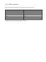
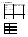
User’s Manual MSC Q7-A50M Qseven Module Rev. 0.6 June 27th, 2013 MSC Qseven-A50M User's Manual General Information Preface Copyright Notice Copyright © 2008 MSC Vertriebs GmbH. All rights reserved. Copying of this document, and giving it to others and the use or communication of the contents thereof, are forbidden without express authority. Offenders are liable to the payment of damages. All rights are reserved in the event of the grant of a patent or the registration of a utility model or design. Important Information This documentation is intended for qualified audience only. The product described herein is not an end user product. It was developed and manufactured for further processing by trained personnel. Disclaimer Although this document has been generated with the utmost care no warranty or liability for correctness or suitability for any particular purpose is implied. The information in this document is provided “as is” and is subject to change without notice. EMC Rules This unit has to be installed in a shielded housing. If not installed in a properly shielded enclosure, and used in accordance with the instruction manual, this product may cause radio interference in which case the user may be required to take adequate measures at his or her own expense. Trademarks All used product names, logos or trademarks are property of their respective owners. Certification MSC Vertriebs GmbH is certified according to DIN EN ISO 9001:2000 standards. Life-Cycle-Management MSC products are developed and manufactured according to high quality standards. Our life-cyclemanagement assures long term availability through permanent product maintenance. Technically necessary changes and improvements are introduced if applicable. A product- change-notification and end-of-life management process assures early information of our customers. Product Support MSC engineers and technicians are committed to provide support to our customers whenever needed. Before contacting Technical Support of MSC Vertriebs GmbH, please consult the respective pages on our web site at www.mscembedded.com for the latest documentation, drivers and software downloads. If the information provided there does not solve your problem, please contact our Technical Support: Phone: +49 - 8165 906 - 200 Fax: +49 - 8165 906 - 201 Email: [email protected] 2 MSC Qseven-A50M User's Manual General Information Content 1 General Information............................................................................................................................... 4 1.1 Revision History .......................................................................................................................... 4 1.2 Reference Documents ................................................................................................................ 4 1.3 Introduction.................................................................................................................................. 5 2 Technical Description ............................................................................................................................ 6 2.1 Key Features ............................................................................................................................... 6 2.2 Block Diagram ............................................................................................................................. 8 2.3 Power Supply .............................................................................................................................. 9 2.4 Power Dissipation ....................................................................................................................... 9 2.5 Mechanical Dimensions ............................................................................................................ 10 2.6 Thermal Specifications .............................................................................................................. 11 2.7 Signal description ...................................................................................................................... 12 2.7.1 High Definition Audio ............................................................................................................ 12 2.7.2 Ethernet ................................................................................................................................ 12 2.7.3 Serial ATA ............................................................................................................................. 13 2.7.4 PCI Express Lanes ............................................................................................................... 13 2.7.5 USB ....................................................................................................................................... 13 2.7.6 LVDS Flat Panel ................................................................................................................... 14 2.7.7 LPC Bus ............................................................................................................................... 15 2.7.8 HDMI ..................................................................................................................................... 15 2.7.9 DisplayPort ............................................................................................................................ 15 2.7.10 Express card support ............................................................................................................ 16 2.7.11 Miscellaneous ....................................................................................................................... 16 2.7.12 Power and System Management.......................................................................................... 17 2.7.13 Power and GND .................................................................................................................... 17 2.8 Connectors ................................................................................................................................ 19 2.8.1 Module connector ................................................................................................................. 19 2.8.2 USB Port assignment ........................................................................................................... 22 3 System Resources .............................................................................................................................. 23 3.1 SMB Address Map .................................................................................................................... 23 3.2 PCI Express Lanes ................................................................................................................... 23 3.3 USB ........................................................................................................................................... 23 3.4 PCI Interrupt Routing Table ...................................................................................................... 24 3.5 IRQ Lines in Legacy IRQ Mode ................................................................................................ 24 3.6 IRQ Lines in APIC Mode ........................................................................................................... 25 4 BIOS .................................................................................................................................................... 26 4.2.2 The Main Menu ..................................................................................................................... 29 4.2.3 The Advanced Menu ............................................................................................................. 30 4.3 Chipset ...................................................................................................................................... 40 4.3.2 Boot ....................................................................................................................................... 46 4.3.3 Security ................................................................................................................................. 47 4.3.4 The Save & Exit Menu .......................................................................................................... 48 4.4 BIOS and Firmware Update ...................................................................................................... 49 4.8 EAPI .......................................................................................................................................... 51 3 MSC Qseven-A50M User's Manual General Information 1 General Information 1.1 Revision History Rev. 0.1 Date th Dec 23 2012 th Description Initial version 0.2 April 11 , 2012 0.3 October 5 , 2012 Added Bios chapter according to Rev. X1.00c ALPHA; LVDS path 0.4 March 1 , 2013 0.5 0.6 Corrections and Enhancements th st th April 8 , 2013 th June 27 , 2013 Updated Bios chapter Updated Bios chapter Enhancements 1.2 Reference Documents [1] Qseven Specification Revision 1.11 th Last update: Nov. 26 2008 [2] PCI Local Bus Specification Rev. 2.1 PCI21.PDF st Last update: June 1 , 1995 http://www.pcisig.com [3] Serial ATA Specification Serial ATA 1.0 gold.pdf th Last update: August 29 , 2002 Rev.1.0 http://www.sata-io.org/ [4] IEEE Std. 802.3-2002 802.3-2002.pdf http://www.ieee.org [5] Universal Bus Specification usb_20.pdf th Last update: April 27 , 2000 http://www.usb.org 4 MSC Qseven-A50M User's Manual General Information 1.3 Introduction Qseven modules are compact, highly integrated Single Board Computers. Typically a Qseven module consists of CPU, chipset, memory, Ethernet controller, BIOS flash, SATA- and USB controller. Interface controllers (e.g. for PCMCIA) or connectors (e.g. RJ45) are implemented on a base board on to which the Qseven module can be mounted. In addition to the power supply PCIe, SATA, USB, LPC etc. interfaces are present on the connector. Thanks to the standardized mechanics and interfaces the system can be scaled arbitrarily. Despite the modular concept the system design is very flat and compact. Qseven modules require a base board to build a working system. For evaluation purposes MSC recommends the official Qseven Reference Platform MSC Q7-MB-RP. This documentation describes the Qseven module Revison 1. 5 MSC Qseven-A50M User's Manual Technical Description 2 Technical Description 2.1 Key Features Core: Processors: AMD G-SeriesT40E dual core (1.0 GHz) on MSC-Q7-A50M-002 and -004 AMD G-SeriesT40R single core (1.0 GHz) on MSC-Q7-A50M-001 AMD G-SeriesT16R single core (615 MHz) on MSC-Q7-A50M-003 Chipset: AMD A50M Memory: DDR3 533MHz, soldered down. 2GB PCI Express Interface: Four PCIe x1 channel Video: Built-in AMD Radeon™ HD 6250 18-24 Bit dual or single channel LVDS via ANX3110 DP-to-LVDS Converter 1x DVI / DisplayPort™ Ethernet: 10/100/1000 Base –T ( Intel 82574, Device ID 8086/10D3 ) Audio: High-Definition Audio USB: 8x USB Ports 2.0 I2C Bus SMBus LPC Bus SATA 2x SATA ports FLASHDrive Optional FerriSSD SATA FLASH 6 MSC Qseven-A50M User's Manual Technical Description BIOS: AMI BIOS with optional TPM support. Supports SPI ROM on base board EEPROM: An SMBus EEPROM is implemented for backup of the CMOS data including user BIOS setup. Realtime Clock: An RTC (integrated in A50M chipset) is available. Watchdog Watchdog with programmable time-out Watchdog enabled via BIOS or application programs System Monitoring: Monitored values: Temperatures (CPU and Board) CPU and system fan speed Fan support: Optional connector on module to run active cooling fan or system fan. Speed control via monitoring device TPM: Optional Infineon TPM 1.2 SuperIO support: The Bios supports the following Super IO chips: Winbond 82627 HF SMSC SCH3114-NU 7 MSC Qseven-A50M User's Manual Technical Description 2.2 Block Diagram Fig. 1: MSC Q7-A50M-001 (T40R) / MSC Q7-A50M-002 (T40E) / MSC Q7-A50M-003 (T16R) Block Diagram 8 MSC Qseven-A50M User's Manual Technical Description 2.3 Power Supply +5V primary power supply input +5V standby 3.3V RTC power supply BIOS SETUP data is stored in a non volatile backup memory device (EEPROM), therefore configuration data will be retained during RTC-Power loss (except for time and date information) Voltage Input range Current +5V +4.75V - 5.25V See next table +5V Standby +4.75V - 5.25 V +3V RTC power supply +2.0V - 3.3V ca. 4uA/ max 6uA 2.4 Power Dissipation CPU: T40E 1.0 GHz RAM: 2GByte Test software: Performance Test Idle Calculation Find prime Number Idle DOS Windows S0 S3 7.2 W 6.0 W 0.3 W Memory Block read 8.4 W 8.4 W Graphic Graphic 2D Graphic complex 3D Graphic test complex test 8.6 W 9.7 W CPU: T40R 1 GHz RAM: 2GByte Idle DOS Windows S0 S3 Idle 8.75 W 6.0 W 0.5 W Calculation Find prime number 9.0 W Memory Block read 10.0 W 9 Graphic Graphic 2D Graphic complex 3D Graphic test complex test 9.25 W 9.75 W MSC Qseven-A50M User's Manual Technical Description 2.5 Mechanical Dimensions The height is dependent on the MXM connector used on the baseboard. Fig. 2: MSC Q7-A50M Mechanical Dimensions 10 MSC Qseven-A50M User's Manual Technical Description 2.6 Thermal Specifications The cooling solution for a Qseven module is based on a heatspreader concept. A heatspreader is a metal plate (typically aluminium) mounted on top of the module. The connection between this plate and the module components is typically made using thermal interface materials such as phase change foils, gap pads and copper or aluminium blocks. A very good thermal conductivity is required in order to transfer the heat from the cpu and the chipset to the heatspreader plate. The heatspreader used by the MSC module is thermally attached using phase change materials and small aluminium blocks filling the gap between cpu and chipset dies and heatspreader plate. The heatspreader is not a heatsink! It is a defined thermal interface for the system designer with fixed mechanical dimensions, so it should be possible to use different module types without problem. The main goal for the thermal design of a system is that each device on the module is operated within its specified thermal limits. The max temperature of CPU and chipset are 90°C, so there may be system implementations where the heatspreader temperature could be higher. In any case it has to be validated that there are no thermal spec violations of any assembled part over the system temperature range even under worst case conditions. 11 MSC Qseven-A50M User's Manual Technical Description 2.7 Signal description In the following tables signals are marked with the power rail associated with the pin, and, for input and I/O pins, with the input voltage tolerance. The pin power rail and the pin input voltage tolerance may be different. An additional label, “Suspend”, indicates that the pin is active during suspend states (S3, S4, S5). If suspend modes are used, then care must be taken to avoid loading signals that are active during suspend to avoid excessive suspend mode current draw. 2.7.1 High Definition Audio Signal Signal Level CMOS CMOS CMOS CMOS Power Rail Core Core Core Core Power PU/PD Tolerance 3.3V 3.3V 3.3V 3.3V Description HDA_RST# HDA_SYNC HDA_CLK HDA_SDO Pin Type Output Output Output Output Reset output to CODEC, active low. 48kHz fixed-rate, sample-synchronization signal to the CODEC(s). 24.00 MHz serial data clock Serial TDM data output to the CODEC. Source / Target A50M A50M A50M A50M HDA_SDI Input CMOS Core 3.3V Serial TDM data inputs from up to 3 CODECs. A50M Signal Level Analog Power Rail 3.3V Sus. Power PU/PD Description Tolerance Gigabit Ethernet Controller 0: Media Dependent Interface Differential Pairs 0,1,2,3. The MDI can operate in 1000, 100 and 10 Mbit / sec modes. Source / Target 82574 2.7.2 Ethernet Signal GBE0_MDI[0:3]+ GBE0_MDI[0:3]- GBE0_ACT# Pin Type Input/ Output Open Drain GBE0_LINK100# Open Drain GBE0_LINK1000# Open Drain GBE0_CTREF REF CMOS CMOS CMOS 3.3V Sus. 3.3V Sus. 3.3V Sus. 3.3V MDI[0]+/B1_DA+/MDI[1]+/B1_DB+/MDI[2]+/B1_DC+/MDI[3]+/B1_DD+/Gigabit Ethernet Controller 0 activity indicator, active low. 82574 3.3V Gigabit Ethernet Controller 0 100 Mbit / sec link indicator, active low. 82574 3.3V Gigabit Ethernet Controller 0 1000 Mbit / sec link indicator, active low. 82574 GND min 3.3V max 82574 (1000MBit) : 1,9V LDO 12 MSC Qseven-A50M User's Manual 2.7.3 Technical Description Serial ATA Signal SATA0_TX+ SATA0_TXSATA0_RX+ SATA0_RXSATA1_TX+ SATA1_TXSATA1_RX+ SATA1_RXSATA_ACT# Pin Type O Signal Level SATA Power Rail 3.3V I SATA 3.3V O SATA 3.3V I SATA 3.3V O CMOS 3.3V 2.7.4 PCI Express Lanes Signal Pin Type O Signal Level PCIe Power Rail Core I PCIe Core I CMOS O CMOS 3.3V Sus. 3.3V Pin Type I/O Signal Level USB Power Rail 3.3V Sus. PCIE_TX[0:3]+ PCIE_TX[0:3]PCIE_RX[0:3]+ PCIE_RX[0:3]PCIE_WAKE# PCIE_RST# 2.7.5 Remark AC coupled on module AC coupled on module AC coupled on module AC coupled on module 3.3V PU/PD Description Serial ATA Channel 0 transmit differential pair. Source / Target A50M Serial ATA Channel 0 receive differential pair. A50M Serial ATA Channel 1 transmit differential pair. A50M Serial ATA Channel 1 receive differential pair. A50M SATA activity indicator, active low. A50M Remark / PU/PD Description Power Tol. AC coupled PCI Express Differential Transmit Pairs 0 to 3 on module AC coupled PCI Express Differential Receive Pairs 0 to 3 off module PCI Express wake event signal Source / Target APU APU Reset signal for external devices USB Signal USB[0:7]+ USB[0:7]- Remark / PU/PD Description Power Tol. 3.3V USB differential pairs, channels 0 through 7 13 Source / Target A50M MSC Qseven-A50M User's Manual Signal Technical Description USB_0_1_OC# Pin Type I Signal Level CMOS Power Rail 3.3V Sus. USB_2_3_OC# I CMOS 3.3V Sus. USB_4_5_OC# I CMOS 3.3V Sus. USB_6_7_OC# I CMOS 3.3V Sus. 2.7.6 Remark / PU/PD Description Power Tol. 3.3V 10k PU USB over-current sense, USB channels 0 and 1. A pull-up for this line is present on the module. An open drain driver from a USB current monitor on the Carrier Board may drive this line low. Do not pull this line high on the Carrier Board. 3.3V 10k PU USB over-current sense, USB channels 2 and 3. A pull-up for this line is present on the module. An open drain driver from a USB current monitor on the Carrier Board may drive this line low. Do not pull this line high on the Carrier Board. 3.3V 10k PU USB over-current sense, USB channels 4 and 5. A pull-up for this line is present on the module. An open drain driver from a USB current monitor on the Carrier Board may drive this line low. Do not pull this line high on the Carrier Board. 3.3V 10k PU USB over-current sense, USB channels 6 and 7. A pull-up for this line is present on the module. An open drain driver from a USB current monitor on the Carrier Board may drive this line low. Do not pull this line high on the Carrier Board. Source / Target A50M A50M A50M A50M LVDS Flat Panel Signal LVDS Channel A differential pairs Source / Target ANX3110 Core LVDS Channel A differential clock ANX3110 LVDS Core LVDS Channel B differential pairs ANX3110 O LVDS Core LVDS Channel B differential clock ANX3110 O CMOS Core 3.3V LVDS panel power enable ANX3110 O CMOS Core 3.3V LVDS panel backlight enable ANX3110 LVDS_BKLT_CTRL O LVDS_A[0:3]+ LVDS_A[0:3]LVDS_A_CK+ LVDS_A_CKLVDS_B[0:3]+ LVDS_B[0:3]LVDS_B_CK+ LVDS_B_CKLVDS_PPEN LVDS_BLEN Pin Type O Signal Level LVDS Power Rail Core O LVDS O Remark / PU/PD Power Tol. Description CMOS Core 3.3V LVDS panel backlight brightness control ANX3110 LVDS_DID_CLK I/O OD CMOS 3.3V 3.3V 10k PU I2C clock output for LVDS display use ANX3110 LVDS_DID_DAT I/O OD CMOS 3.3V 3.3V 10k PU I2C data line for LVDS display use ANX3110 14 MSC Qseven-A50M User's Manual 2.7.7 Technical Description LPC Bus Signal Signal Level CMOS Power Rail Core Remark / PU/PD Power Tol. 3.3V Description LPC_AD[0:3] Pin Type I/O LPC multiplexed address, command and data bus Source / Target A50M LPC_FRAME# O CMOS Core 3.3V LPC frame indicates the start of an LPC cycle A50M LPC_LDRQ# I CMOS Core 3.3V 10k PU LPC serial DMA request, not supported A50M SERIRQ I/O CMOS Core 3.3V 10k PU LPC serial interrupt A50M LPC_CLK O CMOS 3.3V 3.3V LPC clock output - 33MHz nominal A50M 2.7.8 HDMI Signal TMDS_LANE2+ TMDS_LANE2TMDS_LANE1+ TMDS_LANE1TMDS_LANE0+ TMDS_LANE0TMDS_CLK+ TMDS_CLKHDMI_CTRL_CLK HDMI_CTRL_DAT 2.7.9 Pin Type O Signal Level TMDS Power Rail O TMDS O TMDS O TMDS I/O CMOS Core I/O CMOS Core Pin Type O Signal Level PCIe Power Rail O PCIe Remark / PU/PD Description Power Tol. AC coupled Serial Digital Video output differential pair on module shared with signal SDVO_RED+ / SDVO_REDAC coupled Serial Digital Video output differential pair on module shared with signal SDVO_GREEN+ / SDVO_GREENAC coupled Serial Digital Video output differential pair on module shared with signal SDVO_BLUE+ / SDVO_BLUEAC coupled Serial Digital Video clock output differential pair. on module shared with signal SDVO_BCLK+ / SDVO_BCLK3.3V 4K7 HDMI I2C clock line - to set up HDMI peripherals. PU shared with signal SDVO_CTRL_CLK 3.3V 4K7 HDMI I2C data line - to set up HDMI peripherals. PU shared with signal SDVO_CTRL_DAT Source / Target APU Remark / PU/PD Description Power Tol. AC coupled DisplayPort output differential pair on module shared with signal SDVO_RED+ / SDVO_REDAC coupled DisplayPort output differential pair on module shared with signal SDVO_GREEN+ / SDVO_GREEN- Source / Target APU APU APU APU APU APU DisplayPort Signal DP_LANE0+ DP_LANE0DP_LANE1+ DP_LANE1- 15 APU MSC Qseven-A50M User's Manual Signal DP_LANE2+ DP_LANE2DP_LANE3+ DP_LANE3DP_AUX+ DP_AUXDP_HPD# Pin Type O Signal Level PCIe O PCIe I/O PCIe I CMOS Technical Description Power Rail Source / Target APU Core Remark / PU/PD Description Power Tol. AC coupled DisplayPort output differential pair on module shared with signal SDVO_BLUE+ / SDVO_BLUEAC coupled DisplayPort output differential pair. on module shared with signal SDVO_BCLK+ / SDVO_BCLKAC coupled Auxiliary channel differential pair off module shared with signal SDVO_FLDSTALL+ / SDVO_FLDSTALL3.3V Hot plug detection signal that serves as an interrupt request APU APU APU 2.7.10 Express card support Signal EXCD0_CPPE# EXCD0_PERST# Pin Type I O Signal Level 3.3V 3.3V Power Rail Core Core Remark / PU/PD Description Power Tol. 3.3V Express card slot 0 card request 3.3V Express card slot 0 reset Source / Target A50M A50M EXCD1_CPPE# EXCD1_PERST# I O 3.3V 3.3V Core Core 3.3V 3.3V A50M A50M Signal Level CMOS CMOS CMOS CMOS CMOS Power Rail 3.3V 3.3V 3.3V 3.3V 3.3V Remark / PU/PD Power Tol. 3.3V 3.3V 3.3V 3.3V 10k PU 3.3V Description I2C_CLK I2C_DAT SPKR BIOS_DISABLE# WDOUT Pin Type I/O I/O O I O General purpose I2C port clock output General purpose I2C port data I/O line Output for audio enunciator - the "speaker" in PC-AT systems Module BIOS disable input. Pull low to disable module BIOS. Output indicating that a watchdog time-out event has occurred. Microcontroller WDTRIG# I CMOS 3.3V 3.3V Watchdog trigger input. This signal restarts the watchdog timer Microcontroller FAN_TACHOIN FAN_PWMOUT I O CMOS CMOS 3.3V 3.3V Tachometer input Pulse width modulation output for fan speed control A50M A50M Express card slot 1 card request Express card slot 1 reset 2.7.11 Miscellaneous Signal 16 Source / Target MSC Qseven-A50M User's Manual Technical Description 2.7.12 Power and System Management Signal PWRBTN# RSTBTN# Pin Type I I Signal Level CMOS CMOS Power Rail 3.3V Sus. 3.3V Sus. Remark / PU/PD Power Tol. 3.3V 10k PU 3.3V 10k PU SUS_STAT# SUS_S3# SUS_S5# O O O CMOS CMOS CMOS 3.3V Sus. 3.3V 3.3V Sus. 3.3V 3.3V Sus. 3.3V WAKE# BATLOW# THRM# THERMTRIP# SMB_CLK SMB_DAT SMB_Alert SLP_BTN# I I I O I/O I/O I/O I CMOS CMOS CMOS CMOS CMOS CMOS CMOS CMOS 3.3V Sus. 3.3V Sus. 3.3V 3.3V LID_BTN# I BATLOW# PWGIN I I 3.3V 3.3V 3.3V 3.3V 3.3V 3.3V 3.3V 3.3V Sus 10k PU 10k PU 8k2 PU CMOS 3.3V Sus 10k PU CMOS Low<0.6V High>0.8V 3.3V Sus 5V 120k PD 10k PU 10k PU 10k PU Description Source / Target Power button to bring system into a power state. (Negative pulse) Reset button input. Active low input. System is held in hardware reset while this input is low, and comes out of reset upon release. (Negative pulse) Indicates low power suspend operation Indicates system is in Suspend to RAM state. Active low output. Indicates system is in Soft Off state. Also known as "PS_ON" and can be used to control an ATX power supply. External system wake up signal. Indicates that external battery is low. Input from off-module temp sensor indicating an over-temp situation. Active low output indicating that the CPU has entered thermal shutdown. System management clock line System management data line System management bus alert input Sleep button. Low active signal to bring the system in sleep state. (Negative pulse) LID button. Low active signal detect a LID switch to bring the system in sleep state or wake up again.(Low signal) Battery low input indicates a external battery low state Indicates that the external power supply is ready 2.7.13 Power and GND Signal VCC_5V Pin Type Power VCC_5V_SBY Power VCC_RTC Power Signal Level Power Rail 5V (±5%) 5V (±5%) Remark / PU/PD Description Power Tol. Primary power input: +5V (±5%) Standby power input: +5.0V (±5%) All available VCC_5V_SBY pins on the connector(s) shall be used. Used for microcontroller and standby and suspend functions. If no standby power is available connect to VCC_5V Real-time clock circuit-power input : +3.0V (+2.0V to +3.3V) 17 Source / Target Voltage Regulators VCC3.3V SUS regulator MSC Qseven-A50M User's Manual Signal GND Pin Type Power Signal Level Technical Description Power Rail Remark / PU/PD Description Power Tol. Ground - DC power and signal and AC signal return path. All available GND connector pins shall be used and tied to Carrier Board GND plane. 18 Source / Target 2.8 Connectors Qseven Edge Module Connector 2.8.1 Module connector Row A Row B 1 GND 2 GND 3 GBE_MDI3- 4 GBE_MDI2- 5 GBE_MDI3+ 6 GBE_MDI2+ 7 GBE_LINK100# 8 GBE_LINK1000# 9 GBE_MDI1- 10 GBE_MDI0- 11 GBE_MDI1+ 12 GBE_MDI0+ 13 NC 14 GBE_ACT# 15 GBE_CTREF 16 SUS_S5# 17 WAKE# 18 SUS_S3# 19 SUS_STAT# 20 PWRBTN# 21 SLP_BTN# 22 LID_BTN# 23 GND 24 GND KEY KEY 25 GND 26 PWGIN 27 BATLOW# 28 RSTBTN# 29 SATA0_TX+ 30 SATA1_TX+ 31 SATA0_TX- 32 SATA1_TX- 33 SATA_ACT# 34 GND 35 SATA0_RX+ 36 SATA1_RX+ 37 SATA0_RX- 38 SATA1_RX- 39 GND 40 GND 41 BIOS_DISABLE# 42 NC 43 NC 44 NC 45 NC 46 NC 47 NC 48 NC 49 NC 50 NC 51 NC 52 NC 53 NC 54 NC 55 NC 56 NC 57 GND 58 GND 59 HDA_SYNC 60 SMB_CLK 61 HDA_RST# 62 SMB_DAT 63 HDA_BITCLK 64 SMB_ALERT# 65 HDA_SDI 66 I2C_CLK 67 HDA_SDO 68 I2C_DAT 69 THRM# 70 WDTRIG# 71 THRMTRIP# 72 WDOUT 73 GND 74 GND 75 USB_P7- 76 USB_P6- 77 USB_P7+ 78 USB_P6+ 79 USB_6_7_OC# 80 USB_4_5_OC# 81 USB_P5- 82 USB_P4- 83 USB_P5+ 84 USB_P4+ 85 USB_2_3_OC# 86 USB_0_1_OC# 87 USB_P3- 88 USB_P2- 89 USB_P3+ 90 USB_P2+ 91 USB_CL_PRES 92 USB_HC_SEL 93 USB_P1- 94 USB_P0- 95 USB_P1+ 96 USB_P0+ 97 GND 98 GND 99 LVDS_A0+ 100 LVDS_B0+ 101 LVDS_A0- 102 LVDS_B0- 103 LVDS_A1+ 104 LVDS_B1+ 105 LVDS_A1- 106 LVDS_B1- 107 LVDS_A2+ 108 LVDS_B2+ 109 LVDS_A2- 110 LVDS_B2- 111 LVDS_PPEN 112 LVDS_BLEN 113 LVDS_A3+ 114 LVDS_B3+ 115 LVDS_A3- 116 LVDS_B3- 117 GND 118 GND 119 LVDS_A_CLK+ 120 LVDS_B_CLK+ 121 LVDS_A_CLK- 122 LVDS_B_CLK- 123 LVDS_BLT_CTRL 124 RSVD 125 LVDS_DID_DAT 126 LVDS_BLC_DAT 127 LVDS_DID_CLK 128 LVDS_BLC_CLK 129 RSVD 130 RSVD 131 TMDS_CLK+ 132 NC 133 TMDS_CLK- 134 NC 135 GND 136 GND 137 TMDS_LANE1+ 138 DP_AUX+ 139 TMDS_LANE1- 140 DP_AUX- 141 GND 142 GND 143 TMDS_LANE0+ 144 NC 145 TMDS_LANE0- 146 NC 147 GND 148 GND 149 TMDS_LANE2+ 150 HDMI_CTRL_DAT 151 TMDS_LANE2- 152 HDMI_CTRL_CLK 153 DP1_HPD 154 DP1_HPD 155 PCIE_CLK_REF+ 156 PCIE_WAKE# 157 PCIE_CLK_REF- 158 PCIE_RST# 159 GND 160 GND 161 PCIE3_TX+ 162 PCIE3_RX+ 163 PCIE3_TX- 164 PCIE3_RX- 165 GND 166 GND 167 PCIE2_TX+ 168 PCIE2_RX+ 169 PCIE2_TX- 170 PCIE2_RX- 171 EXCD0_PERST# 172 EXCD1_PERST# 173 PCIE1_TX+ 174 PCIE1_RX+ 175 PCIE1_TX- 176 PCIE1_RX- 177 EXCD0_CPPE# 178 EXCD1_CPPE# 179 PCIE0_TX+ 180 PCIE0_RX+ 181 PCIE0_TX- 182 PCIE0_RX- 183 GND 184 GND 185 LPC_AD0 186 LPC_AD1 187 LPC_AD2 188 LPC_AD3 189 LPC_CLK 190 LPC_FRAME# 191 SERIRQ 192 LPC_LDRQ# 193 VCC_RTC 194 SPKR 195 FAN_TACHOIN 196 FAN_PWMOUT 197 GND 198 GND 199 SPI_MOSI 200 SPI_CS0 201 SPI_MISO 202 RSVD 203 SPI_SCK 204 RSVD 205 VCC_5V_SB 206 VCC_5V_SB 207 NC 208 NC 209 NC 210 NC 211 VCC 212 VCC 213 VCC 214 VCC 215 VCC 216 VCC 217 VCC 218 VCC 219 VCC 220 VCC 221 VCC 222 VCC 223 VCC 224 VCC 225 VCC 226 VCC 227 VCC 228 VCC 229 VCC 230 VCC 2.8.2 USB Port assignment Note: The assignment of the USB Ports from Chipset to Q7 connector is as follows: Chipset Q7 Connector Port 0 Port 5 Port 1 Port 3 Port 2 Port 0 Port 3 Port 2 Port 4 Port 6 Port 5 Port 4 Port 6 Port 1 Port 7 Port 7 In Bios setup, all USB port numbers are related to the chipset 3 System Resources 3.1 SMB Address Map Device A6 A5 A4 A3 CMOS backup EEPROM 1 0 1 0 SPD EEPROM (SO-DIMM) 1 0 1 0 *) 8 bit address (with R/W) / 7 bit address (without R/W) A2 1 0 A1 0 0 3.2 PCI Express Lanes Signal /Slot Source PCIE_TX[0] PCIE_RX[0] PCIE_TX[1] PCIE_RX[1] PCIe-Channel 3 APU PCIE_TX[2] PCIE_RX[2] PCIe-Channel 1 APU PCIE_TX[3] PCIE_RX[3] PCIe-Channel 0 APU PCIe-Channel 2 APU 3.3 USB Signal Source / Target Remark USB[0]+ USB[0]USB[1]+ USB[1]USB[2]+ USB[2]USB[3]+ USB[3]USB[4]+ USB[4]USB[5]+ USB[5]USB[6]+ USB[6]USB[7]+ USB[7]- USB0 A50M USB1.1/2.0 USB2 A50M USB1.1/2.0 ) USB1 A50M USB1.1/2.0 USB3 A50M USB1.1/2.0 USB4 A50M USB1.1/2.0 USB5 A50M USB1.1/2.0 USB6 A50M USB1.1/2.0 USB7 A50M USB1.1/2.0 A0 0 0 R/W x x address *) A8h / 54h A0h / 50h PCI Interrupt Routing Table 3.5 HD Audio 14h/02 0 A PCI Express Root Port 0 15h/0 0 A USB OHCI Host Controller 12h/0 0 A USB OHCI Host Controller 13h/0 0 A USB EHCI Host Controller 12h/02 0 B USB EHCI Controller 13h/02 0 B SATA 11h/0 0 A PCI to PCI Host Bridge 0h/07 0 A HD Audio AMD 01h/01 0 B A Bus # IRQ Lines in Legacy IRQ Mode IRQ# Available Typical Interrupt Source 0 No Counter 0 1 No Keyboard 2 No Cascade Interrupt from Slave PIC 3 Yes 4 Yes 5 Yes 6 Yes 7 Yes 8 No RTC 9 Limited In ACPI mode used for SCI 10 Yes 11 Yes PIRQ 7 (INT H) 0 PIRQ 6 (INT G) 01h/01 PIRQ 3 (INT D) Internal Graphic Device PIRQ 2 (INT C) Dev / Func PIRQ 0 (INT A) Slot Number (or Onboard Device) PIRQ 5 (INT F) Interrupts of Controller (TCTC) PIRQ 4 (INT E) Qseven PIRQ 1 (INT B) 3.4 3.6 IRQ# Available 12 Yes 13 No 14 Yes 15 Yes Typical Interrupt Source Math coprocessor IRQ Lines in APIC Mode IRQ# 0 1 2 3 4 5 6 7 8 9 10 11 12 13 14 15 16 17 18 19 20 21 22 23 Available No No No Yes Yes Yes Yes Yes No Yes Yes Yes No No Yes Yes Yes Yes Yes Yes No No No No Typical Interrupt Source Counter 0 Keyboard Cascade Interrupt from Slave PIC Connected to Pin RTC shared SCI Math processor PIRQA PIRQB PIRQC PIRQD 4 BIOS 4.1 Introduction This guide describes the AMI Aptio Setup Startup screen and contains information on how to access Aptio setup to modify the settings which control AMI pre-OS (operating system) functions. 4.1.1 Startup Screen Overview The AMI Aptio Startup screen is a graphical user interface (GUI) that is included in AMI Aptio products. The default bios behavior is to show an informational text screen during bios POST phase, but the graphical boot screen can be enabled in the bios setup. The standard boot screen is a black screen without any logo. 4.1.2 Activity Detection Background While the startup screen is displayed, press the Setup Entry key (F2 or DEL). The system acknowledges the input, and at the end of POST, the screen clears and setup launches. 4.2 Aptio Setup Utility With the AMI Aptio Setup program, you can modify Aptio settings and control the special features of your computer. The setup program uses a number of menus for making changes and turning the special features on or off. This chapter provides an overview of the setup utility and describes at a high-level how to use it. 4.2.1 Configuring the System BIOS To start the AMI Aptio Setup utility, press [F2 or DEL] to launch Setup. The setup main menu appears. The BIOS Menu Structure The BIOS Menu is structured in the following way: Main MSC Board Info Hardware Monitoring Measurement Advanced PCI Subsystem Settings ACPI Settings Trusted Computing CPU Configuration SATA Configuration USB Configuration WB627 SIO Configuration AMI Graphic Output Protocol Policy Chipset North Bridge LVDS Config Select South Bridge Boot Security Save & Exit The Menu Bar The Menu Bar at the top of the window lists these selections: Menu Items Description Main Use this menu for basic system information. Advanced Use this menu to set the Advanced Features available on your system’s chipset. Chipset Use this menu to set Chipset Features. Security Use this menu to set User and Supervisor Passwords and the Backup and Virus-Check reminders. Boot Use this menu to set the boot order in which the BIOS attempts to boot to OS. Save & Exit Saves and Exits the Aptio setup utility. Use the left and right arrow keys on your keyboard to make a menu selection. The Legend Bar Use the keys listed in the legend bar on the right side of the screen to make your selections, or to exit the current menu. The following table describes the legend keys and their alternates: Key Function Esc Exit submenu / Exit Setup utility without saving.. Left and right arrow keys Select Screen. Up and down arrow keys Select Item. +/- Change Option. F1 General Help window. F2 Previous Values F3 Optimized Defaults F4 Save and Exit Select an item To select an item, use the arrow keys to move the cursor to the field you want. Then use the plus-and-minus value keys to select a value for that field. Alternatively the Enter key can be used to select a value from a Pop Up menu. The Save Values commands in the Exit Menu save the values currently displayed in all the menus. Display a submenu To display a submenu, use the arrow keys to move the cursor to the sub menu you want. Then press Enter. A pointer marks all submenus. 4.2.2 The Main Menu You can make the following selections on the Main Menu itself. Use the sub menus for other selections. Feature Options Description Bios Vendor Informative Shows the Bios Vendor Core Version Informative Shows the Aptio Core Version Compliancy Informative Shows the UEFI Compliance Version Project Version Informative Shows the Project Version Build Date Informative Shows the Build Date Total Memory Informative Shows the amount of RAM MSC Board Info Submenu Shows board specific information System Date Enter Date ( MM:DD:YYYY) Set the system date on the real time clock. System Time Enter Time (HH:MM:SS) Set the system time on the real time clock. Access Level Informative This feature shows what kind of user has entered the Aptio setup. It depends on the Security Tab if a Administrator and/or User password is set. 4.2.2.1 MSC Board Info Feature Options Description Manufacturer MSC Vertriebs GmbH Board Name Informative Shows the board name Board Revision Informative Shows the board revision Bios Version Informative Shows the bios version Serial Number Informative Shows the boards serial number Boot Counter Informative Shows the amount of boots EC Bootloader Version Informative Shows the Embedded Controller Bootloader version EC Firmwaer Version Informative Shows the Embedded Controller Firmware version Onboard Lan MAC adresse Informative Shows the onboard Lan MAC adresse UUID Informative Shows the UUID of the system 4.2.2.2 Hardware Monitoring Measurement Feature Options Description CPU Temperature Informative Shows CPU Temperature Chipset Temperature Informative Shows Chipset Temperature CPU Fan Speed Informative Shows the current fan speed 4.2.3 The Advanced Menu Feature Options Description PCI Subsystem Settings Submenu PCI, PCI-X and PCI Express settings ACPI Settings Submenu System ACPI Parameters Trusted Computing Submenu Trusted Computing ( TPM ) settings CPU Configuration Submenu CPU Configuration Parameters SATA Configuration Submenu AHCI SATA Configuration settings USB Configuration Submenu USB configuration parameters Feature Options Description WB627 SIO Configuration Submenu Submenu for Super-IO Winbond W82627 Embedded Controller Features Submenu Embedded Controller Features Serial Port Console Redirection Submenu Serial Port Console Redirection AMI Graphic Output Protocol Policy Submenu Graphic Output adjustment ( appears only if Video Oprom policy is set to UEFI ) 4.2.3.1 PCI Subsystem Settings Submenu Feature Options Description PCI Latency Timer 32, 64, 96, 128, 160, 192, 224, Value to be programmed into PCI 248 PCI Clocks latency timer register VGA Palette Snoop Enabled, Disabled PERR# Generation SERR# Generation PCI Express Settings 4.2.3.1.1 Enabled, Disabled Enabled, Disabled Submenu Enables or disables VGA Palette registers snooping Enables or disables PCI device to generate PERR# Enables or disables PCI device to generate SERR# Configure PCI Express PCI Express Settings Feature Relaxed Ordering Extended Tag No Snoop Options Enabled, Disabled Enabled, Disabled Enabled, Disabled Description Enables or disables PCI Express Device Relaxed Ordering.. If enabled allows device to use 8-bit Tag field as a requester Enables or disables PCI Express Device No Snoop option Maximum Payload Auto, 128, 256, 512, 1024, 2048. 4096 Bytes Set maximum payload of PCI Express Device or allow system Bios to select the value Maximum Read Request Auto, 128, 256, 512, 1024, 2048. 4096 Bytes Set read request size of PCI Express Device or allow system Bios to select the value Feature Options Description ASPM Support Disabled, Auto, Force L0s Set the ASPM level: Force L0s State: Auto: Bios configures ASPM Force L0s: L0s will be forced Disabled: No ASPM will be used Extended Synchronization Enabled, Disabled Enabled allows generation of extended synchronization patterns Link Training Retry Disabled, 2, 5, 10 Defines number of retry. Attempt software will take to retrain the link if previous training attempt was unsuccessful. Link Training Timeout 10us to 1000us Defines number of microseconds software will wait before polling “Link Training” bit in link status register. Value range from 10 to 1000us. Unpopulated Links Kepp Link ON, Disable Link In order to save power, software will disable unpopulated PCI Express links, if this option set to disabled. Restore PCIe Register Enabled, Disabled On non-PCI Express aware OS ‘s ( Pre Windows Vista) some devices may not be correctly reinitialized after S3. Enabling this restores PCIe device configurations on S3 resume. 4.2.3.2 ACPI Settings Feature Enable ACPI Auto Conf Enable Hibernation ACPI Sleep State Lock Legacy Resources LID Switch Support Options Enabled, Disabled Description Enables or disables BIOS ACPI Auto Configuration. Enabled, Disabled Enables or disables system ability to Hibernate (OS/S4 Sleep State). This option may not effective with some OS. Suspend Disabled, S1 (CPU Stop Clock), S3 (Suspend to RAM) Select the highest ACPI Sleep state the system will enter, when the Suspend button is pressed. Enabled, Disabled Enables or disables lock of Legacy parameters. Disabled, Active High, Active Define the behavior of the LID switch. Low Active High = Lid is open with high level Active low= Lid is open with low level 4.2.3.3 TPM Feature TPM Support Options Enabled, Disabled Description Enables or disables TPM support. OS will not show TPM. Reset of platform is required For more information see also technotes in chapter 4.9 TPM state Pending Operation Enabled, Disabled None, Enable take ownership Disable take ownership TPM clear Turn TPM Enable/Disable. NOTE: Your Computer will reboot during restart in order to change State of TPM. Schedule an operation for the Security Device. Note : Your computer will reboot during restart in order to change State of Security Device. 4.2.3.4 CPU Configuration Note: Dependent on used CPU, available setup options may vary Feature Options Description PSS Support Enabled, Disabled Enables or disables the generation of the _PPC, _PSS and _PCT objects. PState Adjustment PState 0, PState 1 Provide to adjust startup P_state level PPC Adjustment NX Mode PState 0, PState 1 Enabled, Disabled Provide to adjust _PPC object for ACPI OS. Enables or disables NO-execute page protection function. SVM Mode Enabled, Disabled Enable or disables CPU virtualization. C6 Mode Enabled, Disabled Enables or disables C6 CPB Mode Auto, Disabled Auto/disable CPB Node 0 Information Submenu View CPU and Cache Information related to Node 0 4.2.3.5 SATA Configuration Feature Options Description SATA Port 0 Informative Shows the SATA Device on Port 0 SATA Port 1 Informative Shows the SATA Device on Port 1 SATA Port 2 Informative Shows the SATA Device on Port 2 4.2.3.6 USB Configuration Feature Options Description Legacy USB Support Enabled, Disabled Enables Legacy USB support. AUTO option disables legacy support if no USB devices are connected. DISABLE option will keep USB devices available only for EFI applications. EHCI Hand-off Enabled, Disabled This is a workaround for OSes without EHCI hand-off support. The EHCI ownership change should be claimed by EHCI driver. Port 60/64 Emulation Enabled, Disabled Enables I/O port 60h/64h emulation support. This should be enabled for the complete USB keyboard legacy support for non-USB aware OSes. USB transfer time-out 1,5,10,20 sec The time-out value for Control, Bulk, and Interrupt transfers. Device reset time-out 10,20,30,40 sec USB mass storage device Start Unit command time-out. Device power-up delay Auto, Manual Maximum time the device will take before it properly reports itself to the Host Controller. 'Auto' uses default value: for a Root port it is 100 ms, for a Hub port the delay is taken from Hub descriptor. Device power-up delay Value 1-40 Delay range is 1…40 seconds, in one second increments. USB Mass Storage Auto, Floppy, Forced FDD, Select Mass storage device emulation Device ( e.g USB Stick) Hard Disk, CD-ROM type. Auto enumerates devices according to their media format. Optical drives are emulated as CDROM, drives with no media will be emulated according to a drive 4.2.3.7 Winbond WB627 / SMSC3114 SuperIO Configuration (if available on carrier board) Feature Options Description COM A: Enabled, Disabled Enable or disable COM A on Winbond SIO COM A Setting: Auto, Resource setting for COM A on Winbond SIO I/O 3F8h, IRQ 4 I/O 3F8h, IRQ 3, 4, 5, 6, 7 ,8 ,10, 11, 12 I/O 2F8h, IRQ 3, 4, 5, 6, 7 ,8 ,10, 11, 12 I/O 3E8h, IRQ 3, 4, 5, 6, 7 ,8 ,10, 11, 12 I/O 2E8h, IRQ 3, 4, 5, 6, 7 ,8 ,10, 11, 12 COM B: Enabled, Disabled Resource setting for COM A on Winbond SIO COM B Setting: Auto, Resource setting for COM A on Winbond SIO I/O 2F8h, IRQ 3 I/O 3F8h, IRQ 3, 4, 5, 6, 7 ,8 ,10, 11, 12 I/O 2F8h, IRQ 3, 4, 5, 6, 7 ,8 ,10, 11, 12 I/O 3E8h, IRQ 3, 4, 5, 6, 7 ,8 ,10, 11, 12 I/O 2E8h, IRQ 3, 4, 5, 6, 7 ,8 ,10, 11, 12 LPT: Disabled, Enabled Enable or disable LPT on Winbond SIO LPT Setting: Auto, Resource setting for LPT A on Winbond SIO I/O 378h, IRQ 5, 7 I/O 278, IRQ 5, 7 Feature LPT Mode: Options Description SPP, EPP 1.9, Mode setting for LPT on Winbond SIO ECP, ECP + EPP 1.9, Printer Mode, EPP 1.7, ECP+EPP 1.7 4.2.3.8 Embedded Controller Features Feature Options Description Watchdog Start on Boot No, Yes Start the watchdog after BIOS Post if enabled. Startup Delay Value 1s, 10s, 30s, 1min, 5min Select the initial delay value. This is an additional one-time delay before the standard timeout timer is started. Event Timeout Value 1s, 10s, 30s, 1min, 5min Select the timeout value after which the watchdog will be execiting its event action Reset Timeout Value 1s, 10s, 30s, 1min, 5min Select the timeout value after whicj the watchdog will be executing its reset action. This timeout will start to countdown after the event timeout expired. After Power Fail Stay Off, Power On, Last State Define the behaviou of the system after a power failure 4.2.3.9 Serial Port Console Redirection Feature Options Description Com 0 Console Redirection Enabled, Disabled Console Redirection Enable or Disable Console Redirection settings Com 0 Submenu The settings specify how the host computer and the remote computer (which the user is using) will exchange data. Both computers should have the same or compatible settings. Serial Port for Out-of Band Management/Windows Emergency Management Service (EMS) Enabled, Disabled Console Redirection Enable or Disable Console Redirection Feature Console Redirection Settings Options Submenu Description The settings specify how the host computer and the remote computer (which the user is using) will exchange data. Both computers should have the same or compatible settings. 4.2.3.9.1 Console Redirection Settings COM0 Submenu Feature Terminal Type Bits per second Options ANSI, VT100, VT100+, VTUTF8 9600, 19200, 38400, 57600, 115200 Description Emulation: ANSI: Extended ASCII char set. VT100: ASCII char set. VT100+: Extends VT100 to support color, function keys, etc. VT-UTF8: Uses UTF8 encoding to map Unicode chars onto 1 or more bytes. Selects serial port transmission speed. The speed must be matched on the other side. Long or noisy lines may require lower speeds. Data Bits 7, 8 Data Bits Parity None, Even, Odd, Mark, Space A parity bit can be sent with the data bits to detect some transmission errors. Even: parity bit is 0 if the num of 1's in the data bits is even. Odd: parity bit is 0 if num of 1's in the data bits is odd. Mark: parity bit is always 1. Space: Parity bit is always 0. Mark and Space Parity do not allow for error detection. They can be used as an additional data bit. Stop Bits 1,2 Stop bits indicate the end of a serial data packet. (A start bit indicates the beginning). The standard setting is 1 stop bit. Communication with slow devices may require more than 1 stop bit. Flow Control None, Hardware Flow control can prevent data loss from buffer RTS/CTS, overflow. When sending data, if the receiving buffers are full, a 'stop' signal can be sent to stop the data flow. Once the buffers are empty, a 'start' signal can be sent to re-start the flow. Hardware flow control uses two wires to send start/stop signals. VTUF8 Combo Key Support Enabled, Disabled, Enable VT-UF8 Combination Key Support for ANSI/VT100 terminals Recorder Mode Disabled, Enabled With this mode enabled only text will be sent. This is to capture Terminal data. Resolution 100x31 Disabled, Enabled Enables or disables extended terminal resolution Legacy OS Redirection 80x24, 80x25 On Legacy OS, the number of rows and Columns supported redirection Feature Options Description Putty KeyPad VT100, Linux, XTERMR6, SCO, ESCN, VT400 Select FunctionKey and KeyPad on Putty. Redirection after Bios Post Always Enable, Boot Loader The settings specify if Bootloader is selected than legacy console redirection is disabled before booting to legacy OS. 4.2.3.9.2 Console Redirection EMS Feature Options Description Out-of-Band Mgmt Port COM0, COM1 Microsoft Windows Emergency Management Services (EMS) allows for remote management of a Windows Server OS through a serial port. Terminal Type ANSI, VT100, VT100+, VTUTF8 Emulation: ANSI: Extended ASCII char set. VT100: ASCII char set. VT100+: Extends VT100 to support color, function keys, etc. VT-UTF8: Uses UTF8 encoding to map Unicode chars onto 1 or more bytes. Bits per second Flow Control 9600, 19200, 57600, 115200 None, Hardware RTS/CTS, Software Xon/Xoff Selects serial port transmission speed. The speed must be matched on the other side. Long or noisy lines may require lower speeds. Flow control can prevent data loss from buffer overflow. When sending data, if the receiving buffers are full, a 'stop' signal can be sent to stop the data flow. Once the buffers are empty, a 'start' signal can be sent to re-start the flow. Hardware flow control uses two wires to send start/stop signals. 4.2.3.10 AMI Graphic Output Protocol Policy Note: This setup item appears only if Video Oprom Policy under CSM settings is set to UEFI. Feature Output Select Options DFP1_DVI, LCD1_LVDS Description Select what first (on Boot) output interface should be used 4.3 Chipset Feature Options Description North Bridge Submenu North Bridge Parameters LVDS Config Select Submenu LVDS Settings South Bridge Submenu South Bridge Parameters 4.3.1 North Bridge Feature Options Description Primary Video Device IGD Video, NB Select Primary Video device that BIOS will use for PCIe slot device output Memory Clock Auto, 400 MHz, 533 MHz, 667 MHz This option allows user to select different memory clocks. SPD : 400 MHz: DDR 800 533 MHz: DDR 1066 667 MHz: DDR 1333 Memory Clear Not cleared, Cleared Memory clear functionality control Memory Information Informative Shows Information about size and clock of the memory GFX / PCIe Configuration Submenu GFX / PCIe configuration Socket 0 Information Informative View information related to socket 0 4.3.1.1 GFX / PCIe Configuration Feature Options Description NB GPP Core Config Disabled, NB GPP Core configuration GPP_Core_x4x 4; GPP_CORE_x4 x2x2; GPP_CORE_x4 x2x1x1; GPP_CORE_x4 x1x1x1x1 DP0 Output Mode DP, eDP, Single NB PCIE connect type ( Display device ) Link DVI-D, HDMI, Travis DP-to-LVDS, Single Link DVII, LVDS, Disabled DP, Single Link DVI-D, HDMI, Travis DP-toLVDS, Single Link DVI-I, Disabled NB PCIE connect type ( Display device ) Port 4-7 Control Enabled, Disabled Port 4/5/6/7 enabled/disabled ASPM Mode Control Disabled, L0s Entry, L1 Entry, L0s and L1 Entry NB root port ASPM mode control Hotplug Mode Control Disabled, Hotplug-Basic, Server, Enhanced, Inboard NB root port hotplug mode Link Speed Max Speed, Gen1, Gen2 NB root port Pcie link speed, the link speed may overwritten by Pspp settings PSPP Policy Disabled, Performance, Balanced-High, Balanced-Low, Power Saving PCIe speed power policy DP1 Output Mode 4.3.1.2 LVDS Config Select Feature Options Description LVDS Parameters Method EDID EEPROM, Select Method to get LVDS Timing LVDS Panel Type List LVDS Panel Type 640x480, 800x480, 800x600, 1024x768, 1280x720, 1280x800, 1280x1024, 1366x768, 1440x900, 1600x900, 1920x1080 LVDS Mapping 18 bit, 24 bit, Select LVDS mapping type 24bit FPDI LVDS Backlight Brightness Control Enabled, Disabled Enable / Disable Brightness Control LVDS Backlight Brightness Polarity Normal Inverted Set PWM Polarity for Brightness Control LVDS Backlight Brightness 0%-100% in 10% steps Select the initial backlight brightness for the LFP panel. Note: Graphics driver may change this brightness setting. Select LVDS Panel resolution 4.3.1.3 South Bridge Feature Options Description SB SATA Configuration Submenu Options for SATA Configuration SB USB Configuration Submenu Options for USB Configuration SB GPP Port Configuration Submenu Options for GPP Port Configuration SB HD Azalia Configuration Submenu Options for SB HD Azalia Configuration SB Debug Configuration Submenu Options for SB Debug Configuration SB Hardware Monitor Control Submenu SB Hardware Monitor Control SB Clock Spread Spectrum Disabled, Enabled Enable SB Clock spread spectrum 4.3.1.3.1 SB SATA Configuration Feature Options Description OnChip SATA Channel Enabled, Disabled Enable or Disabled SATA OnChip SATA Type AHCI, Legacy IDE, Native IDE Select the SATA controller operating mode Disabled, Enabled Enable or disable SATA ESP on Port 0 SATA ESP on Port 1 Disabled, Enabled Enable or disable SATA ESP on Port 1 SATA ESP on Port 2 Disabled, Enabled Enable or disable SATA ESP on Port 2 SATA Power on Port 0 Disabled, Enabled Enable or disable SATA Power on Port 0 SATA Power on Port 1 Disabled, Enabled Enable or disable SATA Power on Port 1 SATA Power on Port 2 Disabled, Enabled Enable or disable SATA Power on Port 2 SATA Port0 Mode Auto, Gen1, Gen2 Forces the SATA Port to run at Gen1 mode if this option is set. Setting to Auto will leave the Port to run at default mode. SATA Port1 Mode Auto, Gen1, Gen2 Forces the SATA Port to run at Gen1 mode if this option is set. Setting to Auto will leave the Port to run at default mode. SATA Port2 Mode Auto, Gen1, Gen2 Forces the SATA Port to run at Gen1 mode if this option is set. Setting to Auto will leave the Port to run at default mode. SATA Ports Auto Clock Disabled, Enabled SATA Ports Auto Clock Control SATA ESP on Port 0 4.3.1.3.2 SB USB Configuration Feature Options Description OHCI HC (Bus 0 Dev 18) Enabled This Port is always enabled OHCI HC (Bus 0 Dev 19) Enabled, Disabled Enable or disable OHCI HC (Bus 0 Dev 19) Feature Options Description USB Port 0 Enabled, Disabled Enable or disable Port 0 USB Port 1 Enabled Enable or disable Port 1 USB Port 2 Enabled, Disabled Enable or disable Port 2 USB Port 3 Enabled, Disabled Enable or disable Port 3 USB Port 4 Enabled, Disabled Enable or disable Port 4 USB Port 5 Enabled, Disabled Enable or disable Port 5 USB Port 6 Enabled, Disabled Enable or disable Port 6 USB Port 7 Enabled, Disabled Enable or disable Port 7 USB Device Wakeup from S3 or S4 Enabled, Disabled Enable or disable USB Device Wake up from S3 or S4. 4.3.1.3.3 SB GPP Port Configuration Feature Options Description SB GPP Function Enabled, Disabled Enable or disable SB GPP Function NB-SB PHY PLL Power Down Enabled, Disabled Enable or Disable NB-SB PHY PLL Power Down SB GPP PHY PLL Power Down Enabled, Disabled Enable or Disable SB PHY PLL Power Down SB GPP Port A ASPM Enabled, Disabled Enable or Disable SB GPP Port A ASPM 4.3.1.3.4 HD Audio Azalia Configuration Feature Options Description HD Audio Azalia Device Enabled, Disabled, Auto Enable or Disable HD Audio Azalia Device HD Onboard Pin Config Enabled, Disabled Enable or Disable HD Onboard Pin Config Azalia Snoop Enabled, Disabled Enable or Disable Azalia Snoop 4.3.1.3.5 Hardware Monitor Control Feature Options Description IMC Fan Control Enabled, Disabled IMC Fan Control ( if disabled, EC is also disabled ) Zone 0 Support Enabled, Disabled Zone 0 Support Help Zone 0 Config Submenu Zone 0 Config 4.3.1.3.6 Zone 0 Config Feature Options Description Zone 0 Fan Speed Mode Linear Mode, Step Mode Set fan speed to linear mode or step mode Fan Frequency From 11Hz up to 28,64Khz Fan PWM Frequency Zone 0 Temperature Average Enabled, Disabled Enable temperature averaging for the temperature sensor Zone 0 Hysteresis 0-16 Active cooling hysteresis temperature in degree Celsius Zone 0 PWM Step Rate 0-100 Fan PWM stepping rate in unit of PWM level percentage ( 0 to 100% ) CPU _AC0 0-100 AC0 is the 1 or highest temperature threshold in degrees of Celsius CPU _AC1 0-100 AC1 is the 2 Celsius CPU _AC2 0-100 AC3 is the 3th temperature threshold in degrees of Celsius st nd temperature threshold in degrees of Feature Options Description th CPU _AC3 0-100 AC4 is the 4 temperature threshold in degrees of Celsius CPU _CRT 0-100 CRT is the critical temperature threshold in degrees of Celsius CPU AL0 0-100 AL0 PWM level in percentage ( 0 to 100% ). This is to be applied when temperature threshold _AC0 is reached. The value is meaningful only if that threshold is defined. CPU AL1 0-100 AL1 PWM level in percentage ( 0 to 100% ). This is to be applied when temperature threshold _AC1 is reached. The value is meaningful only if that threshold is defined. CPU AL2 0-100 AL2 PWM level in percentage ( 0 to 100% ). This is to be applied when temperature threshold _AC2 is reached. The value is meaningful only if that threshold is defined. CPU AL3 0-100 AL3 PWM level in percentage ( 0 to 100% ). This is to be applied when temperature threshold _AC3 is reached. The value is meaningful only if that threshold is defined. 4.3.2 Boot Feature Options Description Setup Prompt Timeout 0-65535sec Number of seconds to wait for setup activation key. 65535(0xFFFF) means indefinite waiting. Bootup NumLock State On, Off Select the keyboard NumLock state Quiet Boot Enabled, Disabled Enables/Disables Quiet Boot option Fast Boot Enabled, Disabled Enables/Disables boot with initialization of a minimal set of devices required to launch active boot option. Has no effect for BBS boot options. For more information see also technotes in chapter 4.9 Boot Option# Bootdevice x Set the system boot order Note: The number of available Boot options is dependent on the devices which are connected. CSM16 Parameters Submenu CSM16 configuration: Enable/Disbale Option Rom execution settings, etc. CSM Parameters Submenu Oprom execution, boot options filter, etc. 4.3.2.1 CSM16 Parameters Feature Options Description GateA20 Active Upon Request, Always UPON Request – GA20 can be disabled using BIOS services. Always – do not allow disabling GA20; this option is useful when any RT code is executed above 1MB Option ROM Messages Force Bios, Keep current Set display mode for option ROM Interrupt 19 Capture Enabled, Disabled Enabled: Allows option ROMs to trap Int 19 4.3.2.2 CSM Parameters Feature Options Description Launch CSM Auto, Always, Never This option controls if CSM will be launched Boot option filter UEFI and Legacy, Legacy only, UEFI only This option controls what devices system can boot to. Launch PXE OPROM policies Do not launch, UEFI only, Legacy only Controls the execution of UEFI and Legacy PXE OPROM Launch Storage OPROM Do not launch, UEFI only, Legacy only Controls the execution of UEFI and Legacy Storage OPROM Launch Video OPROM Do not launch, UEFI only, Legacy only Controls the execution of UEFI and Legacy Video OPROM. Other PCI device ROM 4.3.3 IF set to UEFI, Graphic output can be adjusted in Menu “Advanced / AMI Graphic Output Protocol Policy” UEFI OpROM, For PCI devices other than Network, Mass storage Legacy OpROM or Video defines which OpROM to launch. Security Feature Options Description Administrator Password Set Password Set Setup Administrator Password User Password Set Password Set User Password 4.3.4 The Save & Exit Menu The following sections describe each of the options on this menu. Save Changes and Exit After making your selections in the setup menus, always select "Exit Saving Changes". This procedures stores the selections displayed in the menus in a flash. The next time you boot your computer, the BIOS configures your system according to the setup selections stored in flash. If you attempt to exit without saving, the program asks if you want to save before exiting. During boot-up, the Aptio BIOS attempts to load the values saved in flash. If those values cause the system boot to fail, reboot and press <ESC or DEL> to enter Setup. In Setup, you can get the Default Values (as described below) or try to change the selections that caused the boot to fail. Discard Changes and Exit Exit system setup without saving any changes. Save Changes and Reset When you have completed the system configuration changes, select this option to save the changes and reboot the system, so the new system configuration parameters can take effect. Discard Changes and Reset Select this option to quit Aptio™ TSE without making any modifications to the system configuration Save Changes Selecting “Save Options” saves all the selections without exiting Setup. You can return to the other menus if you want to review and change your selections. Discard Changes Discard changes done so far to any of the setup options Restore Defaults Restore/load default values for all the setup options Restore User Defaults Restore the User defaults to all the setup options. Save as User Defaults Save changes done so far as User defaults. Boot Override It will display all the available boot options from the Boot Option List. The user can select any of the options to select to the particular device and boot directly from it. Launch EFI Shell from filesystem device Attempts to Launch EFI Shell application (Shellx64.efi) from one of the available filesystem devices. 4.4 BIOS and Firmware Update If a System-BIOS update is required please follow these instructions: - Bios Update from DOS: Create a bootable DOS disk, USB Stick or hard disk and unpack the update tool AFUDOS.exe from AFUx64_301.msi Copy the files “afudos.exe”, “uefi.rom” and “update.bat” to this device. Boot the system from this device. Type “update” to update the System Bios. When the Bios update has finished, reboot the system. - Bios Update under Windows: Copy the afuwingui.exe, amifldrv32.sys and the bios image uefi.rom to a storage media (e.g USB stick). Boot Windows XP or Windows 7. Copy the 3 files from your storage media to your Harddisk Run afuwingui.exe. Make sure that no other application is running to avoid crashes during the update procedure. Select “Open” and choose the bios image file uefi.rom. After it has opened, a new Tab Window will be displayed where you can choose what block options should be updated. To make sure all relevant updates will be updated, select “Program all Blocks”. All Blocks should be marked now. Click the Button “Flash” and Bios update will start. After update is finished ( all blocks are green ), restart your system. Note: The Amiflash tool for windows can be downloaded from www.ami.com - Bios Update from EFI Shell Create a FAT32 formatted removable device and unpack the update tool AfuEfix64.efi from AFUx64_301.msi Copy an EFI Shell ( shellx64.efi) into the root directory of the device. Copy the files “Afuefix64.efi”, “uefi.rom” , “update.nsh” to this device. Enter System setup and under the menu bar “Save and Exit” choose Launch EFI Shell from filesystem device. After Shell is loaded, type: - fs0: - update.nsh When the Bios update has finished, reboot the system. Note: If an EFI Shell is needed for Bios updates, please contact MSC Technical support. Note: After the system has been updated, the setup settings will be changed to defaults and therefore it may be necessary to enter Setup to reconfigure the system settings. 4.5 Blind Restoration of Bios default settings (no display available) - Power up the System Repeatedly press DEL for several seconds Press F3 for default settings or F2 for previous values. Press Enter Press F4 Press Enter System will restart 4.6 Restore Bios settings from file It is possible to save configured Bios settings and copy these settings to other boards which have the same Bios version. - Configure the setup as required - Load DOS or EFI Shell with afudos.exe ( for DOS ) or afuefix64.efi ( for EFI Shell ). - Run afudos.exe/afuefix64.efi with following switch to save current Bios: Afudos.exe filename /o Afuefix64.efi filename /o - To copy these Bios settings onto another module run afudos.exe or afuefix64.efi with following switch: Afudos.exe filename /n /R Afuefix64.efi filename /n /R Only the Bios settings will be updated without flashing the complete Bios. If complete Bios update is also needed, additional switches are needed : Afudos.exe uefi.rom /gan Afuefix64.efi filename /p /b /n /x 4.7 Post Codes For Post Code information please contact MSC Technical Support Phone: +49 - 8165 906 - 200 Fax: +49 - 8165 906 - 201 Email: [email protected] 4.8 EAPI The "Embedded Application Programming Interface" (EAPI) used by this module provides a standardized interface for customer applications. This interface allows a user mode application access to hardware specific information as well as hardware resources. Following features are supported: - view board information - access to NVRAM - access to I2C - control backlight - set watchdog timer - view sensor values of hardware monitor MSC provides a software package which is downloadable here after registration http://www.mscembedded.com/de/support-center/qseven/msc-q7-a50m.html Note: I2C function is realized by using GPIO’s, so I2C Clock speed is dependent on CPU speed, system load and power scheme. Normally it is round about 90 KHz. 4.9 Tech Notes 1. Trusted Platform Module (TPM) A TPM is a cryptoprocessor that can store cryptographic keys that protect information. The Trusted Platform Module offers facilities for the secure generation of cryptographic keys, and limitation of their use, in addition to a hardware pseudo-random number generator. It also includes capabilities such as remote attestation and sealed storage. "Remote attestation" creates a nearly unforgeable hash-key summary of the hardware and software configuration. The program encrypting the data determines the extent of the summary of the software. This allows a third party to verify that the software has not been changed. "Binding" encrypts data using the TPM endorsement key, a unique RSA key burned into the chip during its production, or another trusted key descended from it. "Sealing" encrypts data in similar manner to binding, but in addition specifies a state in which the TPM must be in order for the data to be decrypted (unsealed). Software can use a Trusted Platform Module to authenticate hardware devices. Since each TPM chip has a unique and secret RSA key burned in as it is produced, it is capable of performing platform authentication. For example, it can be used to verify that a system seeking access is the expected system. 2. ASPM ( Active State Power Management ) Active State Power Management or ASPM is a power management protocol used to manage PCI Express-based serial link devices as links become less active over time. As serial-based PCIe bus devices, such as IEEE1394 (FireWire), become less active, it is possible for the computer's power management system to take the opportunity to reduce overall power consumption by placing the link PHY into a low-power mode and instructing other devices on the link to follow suit. List of references 5. ASPM http://en.wikipedia.org/wiki/Active_State_Power_Management 10. TPM http://en.wikipedia.org/wiki/Trusted_Platform_Module For additional help contact MSC Technical Support: Phone: +49 - 8165 906 - 200 Fax: +49 - 8165 906 - 201 Email: [email protected]