1
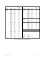
NEX-PCI32
PCI Bus Adapter Users Manual
Including these Software Support packages:
PCI32SW_68
PCI32SW_102
Copyright © 2008 Nexus Technology, Inc. All rights reserved.
Contents of this publication may not be reproduced in any form without the written permission
of Nexus Technology, Inc.
Brand and product names used throughout this manual are the trademarks of their respective
holders.
PCI32-MN-XXX
1
Doc. Rev. 1.10
Warranty Terms and License Agreement
For warranty terms, refer to the Terms and Conditions of Sale document that was included in the
product shipment. The Software License Agreement is displayed during installation. A hardcopy
of that agreement may be obtained from Nexus Technology.
All Nexus Technology products to which this manual refers are subject to the Terms and
Conditions of Sale document and the Software License Agreement, as appropriate.
Compliance with WEEE and RoHS Directives
This product is subject to European Union regulations on Waste Electrical and Electronics
Equipment. Return to Nexus Technology for recycle at end of life. Costs associated with the
return to Nexus Technology are the responsibility of the sender.
PCI32-MN-XXX
2
Doc. Rev. 1.10
TABLE OF CONTENTS
1.0 OVERVIEW ........................................................................................................................... 5
1.1 General Information............................................................................................................ 5
2.0 SOFTWARE INSTALLATION ............................................................................................. 6
2.1 TLA600/700........................................................................................................................ 6
2.2 DAS9200............................................................................................................................. 6
3.0 CONFIGURING the NEX-PCI32 BUS ADAPTER .............................................................. 7
3.1 General Information............................................................................................................ 7
3.2 Configuring for Slot Specific Signals................................................................................. 7
4.0 CONNECTING to the NEX-PCI32 ADAPTER .................................................................... 8
4.1 General................................................................................................................................ 8
4.2 TLA600/700........................................................................................................................ 8
4.3 92A96.................................................................................................................................. 8
5.0 CLOCK SELECTION .......................................................................................................... 10
5.1 General Information.......................................................................................................... 10
5.2 Clocking Options - Explanation ....................................................................................... 10
6.0 VIEWING DATA ................................................................................................................. 11
6.1 Viewing Timing Data on the TLA600/700....................................................................... 11
6.2 Viewing State Data on the DAS9200/TLA500 ................................................................. 12
6.3 Viewing Timing Data on the DAS9200/TLA500.............................................................. 12
7.0 USING the DISASSEMBLY SOFTWARE ......................................................................... 14
7.1 General.............................................................................................................................. 14
7.2 Disassembly Using the TLA600/700................................................................................ 14
7.3 Disassembly Using the DAS9200 / TLA500.................................................................... 17
APPENDIX A - Necessary Signals for Clocking ......................................................................... 18
APPENDIX B - Considerations.................................................................................................... 19
B.1 PCI Loading ..................................................................................................................... 19
B.2 "Patch" Areas ................................................................................................................... 19
B.3 Pattern Generation............................................................................................................ 19
APPENDIX C - Modifying the NEX-PCI32 Adapter .................................................................. 20
APPENDIX D - PCI Local Bus Pinout......................................................................................... 21
APPENDIX E - NEX-PCI32 Mechanical Outline........................................................................ 23
APPENDIX F - Support................................................................................................................ 24
APPENDIX G - References.......................................................................................................... 25
PCI32-MN-XXX
3
Doc. Rev. 1.10
TABLE OF FIGURES
Figure 1- PCI32 MagniVu Display on TLA600/700.................................................................... 11
Figure 2- PCI32 Disassembly ....................................................................................................... 15
Figure 3- PCI32 Disassembly with suppressed Memory and I/O Cycles..................................... 15
TABLE OF TABLES
Table 1- NEX-PCI32 92A96/TLA600/700 Wiring ........................................................................ 9
Table 2- NEX-PCI32 Control Symbol Table................................................................................ 13
PCI32-MN-XXX
4
Doc. Rev. 1.10
1.0 OVERVIEW
1.1 General Information
The NEX-PCI32 adapter has been designed to provide quick and easy connections to interface a
102- or 136-channel TLA600/700, a 92A96, or a 92C96 acquisition module to a 32-bit PCI
backplane. (The PCI designation refers to the Peripheral Component Interconnect Local Bus
specification.) In addition, the method of connection permits the use of other acquisition cards,
pattern generation cards or other measurement devices such as oscilloscopes.
The included NEX-PCI32SW permits the acquisition of all PCI bus cycles, ignoring all Wait and
Idle cycles (although it is possible to acquire these cycles if desired). The software also postprocesses the information to give the user complete disassembly of the bus transactions. Instead
of simply viewing the data in raw form, all cycles are evaluated and, in the case of any
Configuration transactions, complete information on the type of transaction is displayed in easyto-read form.
Please note that this manual uses some terms generically. For instance, references to a 92A96
acquisition card apply to a 92C96 acquisition card; references to the DAS9200 apply equally to
the TLA500; and references to the TLA600/700 apply to a TLA704, TLA711, TLA714,
TLA715, TLA720 or TLA721 chassis with one or more 7*3/4 acquisition cards.
Appendix E is a silk-screen print of the NEX-PCI32 Adapter board. Referring to this drawing
while reading the manual is suggested.
This manual assumes that the user is familiar with the PCI Local Bus specification and the
Tektronix TLA600/700, DAS9200, or TLA500 Logic Analyzer. Also, in the case of the
TLA600/700, it is expected that the user is familiar with M.S. Windows.
For information on using a Prism 32GPX/GPD module with this support, or if 5¼" DAS floppies
are needed, please contact Nexus Technology. See Appendix F for contact information.
PCI32-MN-XXX
5
Doc. Rev. 1.10
2.0 SOFTWARE INSTALLATION
One 3½” diskette has been included with the NEX-PCI32 Bus Adapter. It is for the TLA600/700
series. Diskettes for the DAS9200 or TLA500 are available upon request.
2.1 TLA600/700
The NEX-PCI32SW software is loaded in the same method as other Windows programs. Place
the NEX-PCI32SW Install disk in the floppy drive of the TLA600/700. Select Control Panel
and run Add/Remove Programs, choose Install, Next, then Finish. Add/Remove will then
run SETUP.EXE on the floppy and install the PCI32 support in its proper place on the hard disk.
To load PCI32 support into the TLA600/700, first select the desired Logic Analyzer card in the
Setup screen, select Load Support Package from the File pull-down, then choose PCI32 and click
on Okay. Note that the Logic Analyzer card must be at least 102-channels in width.
2.2 DAS9200
The diskette should be loaded onto the DAS9200 using the Install Application function. This
function is available from the Disk Services menu of the DAS. For more information, refer to the
Tektronix DAS9200 or TLA500 System User's Manual.
Load the desired support from within the 92A96 Config menu by choosing "PCI32 Support" and
pressing <RETURN>. The channel grouping, clocking and symbols will then be loaded.
PCI32-MN-XXX
6
Doc. Rev. 1.10
3.0 CONFIGURING the NEX-PCI32 BUS ADAPTER
3.1 General Information
Not all 32-bit PCI signals are monitored by either the DAS9200 or the TLA600/700. (Refer to
Table 1 for a list of acquired signals.) For information on physically modifying the NEX-PCI32
adapter to monitor signals not provided with the standard implementation, refer to Appendix C.
3.2 Configuring for Slot Specific Signals
A jumper block (JP1) has been provided to enable monitoring the slot specific signals REQ# and
GNT#. To acquire these signals, connect the included flying leads to the appropriate signal pin,
attach a grabber tip to the other end of the wire, then connect the grabber tip to a point on the
backplane or target circuitry to acquire these signals. It may be necessary to refer to schematics
of the target board to determine where the signals can be probed. For reference, the signals may
be acquired on the PCI Bus at the following pins:
GNT#
REQ#
PCI32-MN-XXX
A17
B18
7
Doc. Rev. 1.10
4.0 CONNECTING to the NEX-PCI32 ADAPTER
4.1 General
Although taller than a standard PCI module, the NEX-PCI32 adapter is designed to plug directly
into any PCI backplane slot. The board length and connector spacing conforms to PCI Revision
2.1 specifications.
4.2 TLA600/700
When using a TLA600/700 with a 7*3/4 acquisition module, the necessary acquisition data
sections are A0-A3 and C0-C3. These grouped channels (8 podlets to a group) should be
connected to the locations denoted for the A96. Follow the silk-screened information on the
board that shows the proper relationship between the signal and reference inputs. When properly
connected, the sides of the podlets that have writing on them should be visible.
Connect the four clock leads to their specified locations at J8 (the only connector with 4
locations). Again, follow the silk-screened information to properly connect the clock input and
its ground. Table 1 shows the wiring and Channel Grouping for the TLA600/700 when used with
the NEX-PCI32 adapter.
4.3 92A96
When using a 92A96 or 92C96, connect the grouped pods to their appropriate locations by
following the silk-screen information printed on the adapter board. The 92A/C96 pods are
labeled A0-A3 and C0-C3. Each pod has its proper location denoted on the silk-screen of the
adapter board. When attaching the pods, follow the silk-screen information on the board showing
the ground and signal pin locations. When properly connected, the colored sides of the podlets
should be visible.
Connect the four clock leads (one per A96 cable) to their specified locations at J8 (the only
connector with 4 locations). Again, follow the silk-screened information to properly connect the
clock input and its ground. Table 1 shows the wiring and Channel Grouping for the 92A96 when
used with the NEX-PCI32 adapter.
PCI32-MN-XXX
8
Doc. Rev. 1.10
Group
Signal
PCI
Name
Addr_Dat
(Hex)
Name
AD[31]
AD[30]
AD[29]
AD[28]
AD[27]
AD[26]
AD[25]
AD[24]
AD[23]
AD[22]
AD[21]
AD[20]
AD[19]
AD[18]
AD[17]
AD[16]
AD[15]
AD[14]
AD[13]
AD[12]
AD[11]
AD[10]
AD[9]
AD[8]
AD[7]
AD[6]
AD[5]
AD[4]
AD[3]
AD[2]
AD[1]
AD[0]
Pin #
B20
A20
B21
A22
B23
A23
B24
A25
B27
A28
B29
A29
B30
A31
B32
A32
A44
B45
A46
B47
A47
B48
A49
B52
B53
A54
B55
A55
B56
A57
B58
A58
TLA600/700 /
92A96
input
A3:7
A3:6
A3:5
A3:4
A3:3
A3:2
A3:1
A3:0
A2:7
A2:6
A2:5
A2:4
A2:3
A2:2
A2:1
A2:0
A1:7
A1:6
A1:5
A1:4
A1:3
A1:2
A1:1
A1:0
A0:7
A0:6
A0:5
A0:4
A0:3
A0:2
A0:1
A0:0
Group
Signal
PCI
Name
Control
(Sym)
Aux_0
Aux_1
Name
RST#
FRAME#
DEVSEL#
STOP#
IRDY#
TRDY#
C/BE#[3]
C/BE#[2]
C/BE#[1]
C/BE#[0]
INTD#
INTC#
INTB#
INTA#
REQ#
GNT#
LOCK#
IDSEL
PERR#
PAR
SERR#
CLK
Aux_0:[7-0]
Aux_1:[7-0]
Pin #
A15
A34
B37
A38
B35
A36
B26
B33
B44
A52
B08
A07
B07
A06
--------B39
A26
B40
A43
B42
B16
---------
Clock:0
Clock:1
Clock:2
Clock:3
CLK=
unused
DEVSEL#=
unused
B16
----B37
-----
Intrpt
(Off)
Misc
(Off)
TLA600/700 /
92A96
input
C3:5
C2:0
C3:0
C2:3
C2:1
C2:2
C2:7
C2:6
C2:5
C2:4
C0:3
C0:2
C0:1
C0:0
C0:5
C0:6
C3:4
C0:4
C3:3
C3:2
C3:1
C3:6
D2
D3
Table 1- NEX-PCI32 92A96/TLA600/700 Wiring
PCI32-MN-XXX
9
Doc. Rev. 1.10
5.0 CLOCK SELECTION
5.1 General Information
There are three clocking options available when using the NEX-PCI32SW support package.
Each is explained in detail below.
When using a TLA600/700, the clocking mode is selected by moving to the System window,
clicking on Setup for the appropriate LA card, then clicking on More (a button to the right of the
Clocking field). Choose the desired mode in the Clocking Select field.
When using a DAS9200 or TLA500, the clocking selection is made in the Clock menu. Open the
select field labeled Support Software, choose PCI32, then press <RETURN>.
5.2 Clocking Options - Explanation
Bus Cycle Acquisition - This is the default clocking selection. In this mode only one address
cycle is expected. All Wait and Idle states are ignored. In this clocking mode the High Address
cycle of a Dual Address cycle will not be acquired as it will be considered a Wait state. The Low
Address portion of the cycle will be properly acquired and displayed, as will all data associated
with the cycle. This clocking selection offers the best use of your acquisition memory by
ignoring all Wait and Idle states. Data is acquired on the rising edge of CLK, with DEVSEL#,
FRAME#, IRDY#, and TRDY# used as qualifiers to determine when valid information is
present. These signals must be present for bus cycle acquisitions to be made properly.
Dual Address Capable - In this mode, both the Low Address and High Address parts of a Dual
Address Cycle will be acquired. However, because of the clocking algorithm used, a Wait state
immediately following a valid Address cycle will be acquired as well. The disassembly software
will properly distinguish between a Wait cycle and the High Address portion of a Dual Address
cycle, and will label each appropriately. As with Bus Cycle Acquisition, data is acquired on the
rising edge of CLK, with DEVSEL#, FRAME#, IRDY#, and TRDY# used as qualifiers to
determine when valid information is present. These signals must be present for this mode to
properly acquire data.
Every CLK Rising Edge - In this mode, data will be acquired on every rising edge of the PCI
CLK signal. The disassembly will filter and display these cycles accordingly, incorrect decoding
may occur because of the numerous duplicated cycles. This clocking mode shows all bus cycles,
including Wait and Idle states. Since no clocking qualification is done only the CLK signal is
required.
PCI32-MN-XXX
10
Doc. Rev. 1.10
6.0 VIEWING DATA
6.1 Viewing Timing Data on the TLA600/700
By default, the TLA600/700 will display an acquisition in the Disassembly mode. However, the
same data can be displayed in Timing form by adding a Waveform Display window. This is done
by clicking on the Window pull-down, selecting New Data Window, clicking on Waveform
Window Type, then choosing the Data Source. Two choices are presented: PCI32 and PCI32MagniVu. The first will show the exact same data (same acquisition mode) as that shown in the
Disassembly window, except in Timing format. The second selection, PCI32-MagniVu, will
show all of the channels in 2GHz/8GHz MagniVu mode, so that edge relationships can be
examined at the module’s trigger point. With either selection, all channels can be viewed by
scrolling down the window. Refer to the TLA600/700 System User’s Manual for additional
information on formatting the Waveform display.
Figure 1- PCI32 MagniVu Display on TLA600/700
PCI32-MN-XXX
11
Doc. Rev. 1.10
6.2 Viewing State Data on the DAS9200/TLA500
After an acquisition is made the DAS9200 Logic Analyzer will display the data in State Display
mode (as a default only). Address / Data information is displayed in hexadecimal format; Control
data is displayed using symbols; Interrupt, Miscellaneous, and both Auxiliary data groups default
to OFF.
The use of Symbol Tables when displaying state data enables the user to quickly determine what
type of bus cycle was acquired. A symbol table (PCI32_Ctrl, Table 2) has been provided to show
the type of transaction that occurred on the PCI bus. This symbol table quickly shows whether
the acquisition was a memory or I/O operation, a read or a write, etc.
It is important to note that changing the group, channel, or wiring of the Control group can result
in incorrect symbol information being displayed.
6.3 Viewing Timing Data on the DAS9200/TLA500
It may be useful to display acquired information using the Timing Diagram display of the
DAS9200. (Note that, unlike some other logic analyzers, with the DAS9200 there is no need to
re-acquire PCI data when changing from one display mode to another. The same data can be
viewed in either format.) This method of data display can be particularly useful when an
asynchronous acquisition has been made (using the DAS9200 internal acquisition clock) to
determine the relationships between signal edges.
Refer to the appropriate Tektronix DAS 92A96 Module User's Manual for more detailed
information on formatting the display of the acquired data.
PCI32-MN-XXX
12
Doc. Rev. 1.10
Pattern
0xxxxxxxxx
1011110000
1011110001
1011110010
1011110011
101111010x
1011110110
1011110111
101111100x
1011111010
1011111011
1011111100
1011111101
1011111110
1011111111
1x0x001110
1x0x001101
1x0x001011
1x0x000111
1x0x001100
1x0x000011
1x0x000000
1x0x001111
11xxxxxxxx
10xxxxxxxx
TLA600/700 / 92A96 Symbols
RESET
INTERRUPT ACK
SPECIAL CYCLE
I/O READ ADDRESS
I/O WRITE ADDRESS
RESERVED
MEMORY READ ADDRESS
MEMORY WRITE ADDRESS
RESERVED
CONFIG READ ADDRESS
CONFIG WRITE ADDRESS
MEMORY READ MULTIPLE
DUAL ADDRESS
MEMORY READ LINE
MEMORY WRITE & INVALIDATE
DATA - BYTE 0
DATA - BYTE 1
DATA - BYTE 2
DATA - BYTE 3
DATA - BYTES 0 & 1
DATA - BYTES 2 & 3
DATA - BYTES 0-3
INVALID DATA
FRAME HI
FRAME LO
Meaning
Reset
Interrupt Acknowledge
Special Cycle
I/O Read
I/O Write
Reserved
Memory Read
Memory Write
Reserved
Configuration Read
Configuration Write
Memory Read Multiple
Dual Address Cycle
Memory Read Line
Memory Write & Invalidate
Byte 0 valid (D0-7)
Byte 1 valid (D8-15)
Byte 2 valid (D16-23)
Byte 3 valid (D24-31)
Bytes 0 & 1 valid (D0-15)
Bytes 2 & 3 valid (D16-31)
Bytes 0-3 valid (D0-31)
Invalid Data
Frame Hi
Frame Lo
Table 2- NEX-PCI32 Control Symbol Table
Signals, from left to right: RST#, FRAME#, STOP#, DEVSEL#, IRDY#, TRDY#,
C/BE#[3], C/BE#[2], C/BE#[1], C/BE#[0]
PCI32-MN-XXX
13
Doc. Rev. 1.10
7.0 USING the DISASSEMBLY SOFTWARE
7.1 General
The NEX-PCI32SW support software decodes bus transactions and displays information in
easily understood text form, just like a typical Tektronix microprocessor disassembler (see
Figure 2). All PCI Cycle types are identified and Config Cycles are decoded to reflect the
meaning of the registers. For instance, Command and Status registers are completely evaluated,
with each bit’s state being presented in easy-to-read text. Device information is translated
according to Class, sub-Class, and Type to inform the user as to what device (IDE Disk, Video
controller, network interface, etc.) is being accessed. The C/BE bus signals are also monitored to
determine which data bytes are valid for any given transaction. Invalid bytes are indicated by
dashes in the display, making it much easier for the designer to determine what data is actually
present on the bus at any given time.
It is also possible to filter the data display to show only those cycle types of interest (Figure 3).
The user can choose to display or suppress Memory, I/O, or Config cycles to permit easy and
quick analysis of only those cycles of interest.
Another feature of the NEX-PCI32SW software is its ability to intelligently acquire PCI data. By
taking advantage of the data clocking power built in to the Tektronix Logic Analyzers the PCI32
software is able to acquire only the PCI bus cycles and ignore Idle and Wait states. This means
that the user is able to make optimum use of the acquisition card’s memory and see more bus
transactions. For debug purposes. the user also has the ability to override this function and
acquire data on every PCI CLK rising edge to permit the user to see all of the bus traffic
including the Idle and Wait states. (See Section 5.3 Clocking Options for further information.)
Every stored cycle (bus or rising clock edge, depending upon clocking selection) has a
timestamp value stored with it. This time information, accurate to 125ps/500ps in the
TLA600/700 series, and to 10ns in the DAS9200 / TLA500, permits precise measurements of
bus throughput during burst read transactions, etc. Because of the design of Tektronix Logic
Analyzers there is no need to worry about trading off acquisition memory depth when making
these measurements, as the timestamp memory is separate from the acquisition memory.
7.2 Disassembly Using the TLA600/700
The TLA600/700, since it is a Windows program, has the same type of user interface as other
Windows-based applications. In the Disassembly Listing window, a tool bar at the top of the
window
PCI32-MN-XXX
14
Doc. Rev. 1.10
Figure 2- PCI32 Disassembly
Figure 3- PCI32 Disassembly with suppressed Memory and I/O Cycles
PCI32-MN-XXX
15
Doc. Rev. 1.10
contains buttons that allow the user to modify the display. These buttons, from left to right,
perform the following functions:
Add Column - Adds a column to the display
Add Mark - Adds a user mark to the display
Cut - (may be grayed out) - Cuts the selection to the Clipboard
Copy - (may be grayed out) - Copies the selection to the Clipboard
Paste - (may be grayed out) - Inserts the contents of the Clipboard
Go To - Moves the display to the item of interest
Properties - Edits the current Listing Display properties
Smaller Font - Decreases the displayed font size
Larger Font - Increases the displayed font size
Search Backward - Moves to a previous data match
Define Search - Define data to be matched
Search Forward - Moves to the next data match
Mark Opcode - Permits placing an opcode mark (disabled in PCI32SW)
The format (or display properties) of each displayed column can be changed by putting the
mouse cursor on the heading of the column, clicking the left mouse button to select that column,
clicking the right mouse button to bring up the editing dialog, then selecting Properties. The
column to be modified can also be selected by clicking on the Column tab, selecting the column
of interest in the Column field, then making any desired modifications to that display column.
The modification or selections possible will vary from column to column.
Two display columns of particular interest are the Timestamp and Mnemonics columns.
Timestamp shows a time value associated with the acquisition. By default, Timestamp shows the
time from System Trigger. Clicking on the From window in the Timestamp Reference field
shows all available selections: Absolute (from when the Logic Analyzer was started), Previous
(the time from the present sequence to the previous displayed one), and three selections that
permit time to be displayed from different reference points: System Trigger, Cursor 1 Current
Position, and Cursor 2 Current Position. Selecting the desired mode with the mouse, and then
clicking the left mouse button, will make the selection the present Timestamp display mode.
The other column of interest is the Mnemonics column, where the PCI32 disassembly
information is displayed. As mentioned previously, it is possible to choose which PCI cycles are
displayed. This is done via selections made in the Disassembly tab of the Properties window. By
default the display is in Hardware mode, and Memory, I/O, and Config cycles are set to
Highlight. By choosing something other than Hardware in the Show select field, any cycle type
set to Normal (instead of Highlight) will not be displayed. It is possible, for instance, to display
only Config Cycles by setting Memory and I/O Cycles to Normal, leaving Config Cycles set to
Highlight, and setting the Show select field to Software. All of the data still exists, some has just
been suppressed from view. To return all of the data to visibility, set all Cycle selections to
Highlight.
Note that when data is suppressed in this fashion that Timestamp information (in Previous form)
will be updated to show the time between displayed cycles.
PCI32-MN-XXX
16
Doc. Rev. 1.10
7.3 Disassembly Using the DAS9200 / TLA500
To view PCI32 data in Disassembly form, simply click on the DISASM button in the lower part
of the DAS/TLA display, or select Disasm in the Display column of the Main Menu. All PCI
transactions will be displayed and disassembled, and the Timestamp between each acquisition is
displayed (Relative mode). To change the Timestamp format, press (or click) F5 (Display
Format) and open the Timestamp select field. The options available are: Relative (time from the
previous sample), Delta (time from a user definable Delta mark), Absolute (time from when the
acquisition card was started), and Off. Making a choice, closing the field, then pressing (or
clicking) F8 to Exit and Save will modify the Disassembly display appropriately.
To filter the displayed data, again move to the Display Format screen (press or click F5). The
Hardware Display Mode (default) will display all PCI cycles by default.
By default the display is in Hardware mode, and Memory, I/O, and Config cycles are set to
Highlight. By choosing something other than Hardware in the Display Mode select field, any
cycle type set to Normal (instead of Highlight) will not be displayed. It is possible to display
only Config Cycles by setting Memory and I/O Cycles to Normal, leaving Config Cycles set to
Highlight, and setting the Display Mode select field to Software. All of the data still exists, some
has just been suppressed from view. To return all of the data to visibility, set all Cycle selections
to Highlight.
Note that when data is suppressed in this fashion that Timestamp information (in Relative form)
will be updated to show the time between displayed cycles.
PCI32-MN-XXX
17
Doc. Rev. 1.10
APPENDIX A - Necessary Signals for Clocking
To properly acquire PCI bus activity, the following signals must be provided: CLK, DEVSEL#,
FRAME#, IRDY#, and TRDY#. The rising edge of CLK is used as the only active clocking
edge; all other signals are used to properly qualify the acquisition of data.
PCI32-MN-XXX
18
Doc. Rev. 1.10
APPENDIX B - Considerations
B.1 PCI Loading
It must be noted that the NEX-PCI32 Bus Adapter does not provide any buffering of the PCI
backplane signals. This was a conscious design decision that was made by balancing the
tradeoffs of possible backplane loading versus signal acquisition accuracy. By not introducing
signal buffers it is possible, using the NEX-PCI32 adapter, to see the exact timing relationships
and signal waveforms from the backplane. It is also much easier to connect pattern generators to
the backplane since buffer direction is not a concern. It is believed that the signal loading of the
TLA600/700 or 92A96 acquisition cards is low enough so that PCI signal degradation will not
occur.
The NEX-PCI32 Adapter Board was designed so that the run lengths for critical signals (and
those with the highest activity levels, such as the address / data bus) are as short as possible. This
should help greatly in retaining signal integrity
B.2 "Patch" Areas
If signal loading or reflection does become a concern, the capability exists to add series resistors
to any PCI signal. Patch areas have been provided next to each TLA600/700/A96 connector,
consisting of two rows of plated through holes. These areas (outlined on the silk-screen and
labeled as Nxx) are suitable for individual resistors or resistor networks. To add a series resistor,
simply cut the trace of the desired signal on the component side of the board, and solder the
resistor between the two feed-throughs.
B.3 Pattern Generation
Because there is no buffer circuitry on the NEX-PCI32 Adapter, it is well suited for use with the
92S16 and 92S32 Pattern Generator modules available for the DAS9200. By connecting pattern
generator probes to the A96 signal connectors on the Adapter, desired bus activity can be
simulated. This can be particularly effective when trying to debug interrupt or DMA conflicts.
It should be noted that, because of the pin spacing of the A96 connectors, it is not recommended
that the Tektronix P6464 or P6465 pattern generator probes be used without providing adequate
cooling for their podlets. These probes use active podlets that can get very warm in use. A better
choice would be the P6463 pods which are passive and do not have such cooling requirements.
PCI32-MN-XXX
19
Doc. Rev. 1.10
APPENDIX C - Modifying the NEX-PCI32 Adapter
As previously mentioned, not all PCI signals are acquired by a 92A96 or TLA600/700.
Assumptions have been made as to what signals are of interest, but these assumptions may not be
appropriate for every instance. For these occasions, the NEX-PCI32 adapter may be easily
modified to monitor any desired signals.
To monitor additional signals, the method is fairly simple. All PCI signals have been brought out
to feed-throughs on the board, and there is one unused TLA/A96 connector (J16). This connector
has a patch area beneath it (towards the edge connector) to provide easy solder points. Use wire
wrap wire to connect the PCI signals to this connector.
PCI32-MN-XXX
20
Doc. Rev. 1.10
APPENDIX D - PCI Local Bus Pinout
Information given here is for the 32-bit Universal Board definitions:
Pin #
1
2
3
4
5
6
7
8
9
10
11
12
13
14
15
16
17
18
19
20
21
22
23
24
25
26
27
28
29
30
31
32
PCI32-MN-XXX
Side B - Component Side
-12V
TCK
Ground
TDO
+5V
+5V
INTB#
INTD#
PRSNT1#
Reserved
PRSNT2#
KEYWAY
KEYWAY
Reserved
Ground
CLK
Ground
REQ#
+V I/O
AD[31]
AD[29]
Ground
AD[27]
AD[25]
+3.3V
C/BE[3]#
AD[23]
Ground
AD[21]
AD[19]
+3.3V
AD[17]
Side A - Solder Side
TRST#
+12V
TMS
TDI
+5V
INTA#
INTC#
+5V
Reserved
+V I/O
Reserved
KEYWAY
KEYWAY
Reserved
RST#
+V I/O
GNT#
Ground
Reserved
AD[30]
+3.3V
AD[28]
AD[26]
Ground
AD[24]
IDSEL
+3.3V
AD[22]
AD[20]
Ground
AD[18]
AD[16]
21
Comments
32-bit start
3.3V key
3.3V key
Doc. Rev. 1.10
Pin #
33
34
35
36
37
38
39
40
41
42
43
44
45
46
47
48
49
50
51
52
53
54
55
56
57
58
59
60
61
62
PCI32-MN-XXX
Side B - Component Side
C/BE[2]#
Ground
IRDY#
+3.3V
DEVSEL#
Ground
LOCK#
PERR#
+3.3V
SERR#
+3.3V
C/BE[1]#
AD[14]
Ground
AD[12]
AD[10]
Ground
KEYWAY
KEYWAY
AD[8]
AD[7]
+3.3V
AD[5]
AD[3]
Ground
AD[1]
+V I/O
ACK64#
+5V
+5V
Side A - Solder Side
+3.3V
FRAME#
Ground
TRDY#
Ground
STOP#
+3.3V
SDONE
SBO#
Ground
PAR
AD[15]
+3.3V
AD[13]
AD[11]
Ground
AD[9]
KEYWAY
KEYWAY
C/BE[0]#
+3.3V
AD[6]
AD[4]
Ground
AD[2]
AD[0]
+V I/O
REQ64#
+5V
+5V
22
Comments
5V key
5V key
32-bit end
Doc. Rev. 1.10
APPENDIX E - NEX-PCI32 Mechanical Outline
PCI32-MN-XXX
23
Doc. Rev. 1.10
APPENDIX F - Support
About Nexus Technology, Inc.
Established in 1991, Nexus Technology, Inc. is dedicated to developing, marketing, and
supporting Bus Analysis applications for Tektronix Logic Analyzers.
We can be reached at:
Nexus Technology, Inc.
78 Northeastern Blvd. #2
Nashua, NH 03062
TEL: 877-595-8116
FAX: 877-595-8118
Web site: http://www.nexustechnology.com
Support Contact Information
Technical Support
General Information
Quote Requests
[email protected]
[email protected]
[email protected]
We will try to respond within one business day.
If Problems Are Found
Document the problem and e-mail the information to us. If at all possible please forward
a Saved System Setup (with acquired data) that shows the problem. Do not send a text
listing alone as that does not contain enough data for analysis. To prevent corruption
during the mailing process it is strongly suggested that the Setup be zipped before
transmission.
PCI32-MN-XXX
24
Doc. Rev. 1.10
APPENDIX G - References
Tektronix TLA600/700 System User’s Manual
Tektronix TLA600/700 Module User’s Manual
Tektronix DAS9200 / TLA500 System User’s Manual
Tektronix 92A96 / 92C96 Module User’s Manual
PCI Local Bus Specification
Production Version; Revision 2.1s - June 1, 1995
Published by:
PCI Special Interest Group
PO Box 14070
Portland OR 97214
800-433-5177 (U.S.)
503-797-4207 (International)
503-234-6762 (FAX)
PCI System Architecture
Third Edition
Mindshare, Inc. (Tom Shanley / Don Anderson)
Published by Addison Wesley
ISBN 0-201-40993-3
PCI32-MN-XXX
25
Doc. Rev. 1.10