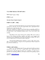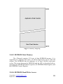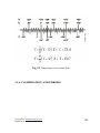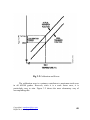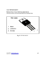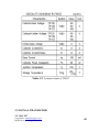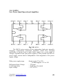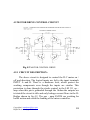
1
FIRE FIGHTING ROBOT A PROJECT REPORT Submitted by S.KANNAN R.KARTHIKEYAN S.SATHISH KUMAR in partial fulfillment for the award of the degree of BACHELOR OF ENGINEERING in ELECTRICAL AND ELECTRONICS ENGINEERING MAHENDRA ENGINEERING COLLEGE, NAMAKKAL. ANNA UNIVERSITY: CHENNAI 600025 MAY 2006 Copyright © [email protected] Duplicate is strictly prohibited 1 ANNA UNIVERSITY: CHENNAI 600025 BONAFIDE CERTIFICATE Certified that this project report “FIRE FIGHTING ROBOT” is the Bonafide work of “ KANNAN.S, KARTHIKEYAN.R, SATHISHKUMAR.S ” who carried out the project work under my Supervision. SIGNATURE SIGNATURE PROF K.K.SELVAM M.S., G.BALAJI B.E., HEAD OF DEPARTMENT SUPERVISOR Electrical and Electronics Engineering, LECT/EEE Mahendra Engineering College, Electrical and Electronics Engineering, Mahendra Engineering College, Mallasamudram (W), Mallasamudram (W), Namakkal (Dt), Namakkal (Dt), Tamil nadu. Tamil nadu Pin code – 637503. Pin code – 637503. Copyright © [email protected] Duplicate is strictly prohibited 2 ACKNOWLEDGEMENT We take this opportunity to express our gratitude to all those who have helped us in completing this project. We are greatly indebted to our magnificent chairman Shri M. G. BHARATHKUMAR, M.A., B Ed., M.I.S.T.E., whose progressive ideal added with the far-sighted counsels of our benevolent secretary Smt. VALLIYAMMAL., M.A., PH.D., DIPLOMA IN FRENCH has shouldered our endeavors and hauled us to meritorious heights. We would like to express our sincere thanks to Prof. K.SUKUMARAN, Principal, Mahendra engineering college, Mallasamudram, for his blessings, which as enabled this project to be a completed one. We express our deep sense of gratitude to Prof. K.K.SELVAM, B.E., MS., Head of the Department, Mahendra engineering college. We are extremely thankful to Ms. G.BALAJI, B.E., our internal guide for her valuable guidance and suggestions throughout the project. No words can adequately express our deep gratitude to Mr.B.N.PRAKASH, B.E., for having consented to guide us. Finally, we sincerely thank our teachers, family members, friends and well wishers for their moral support throughout this project. Copyright © [email protected] Duplicate is strictly prohibited 3 TABLE OF CONTENTS CHAPTER NO 1. TITLE PAGE NO. 1 ABSTRACT i 2 LIST OF FIGURES ii 3 LIST OF TABLES iii 4 LIST OF SYMBOLS iv INTRODUCTION 1 1.1 FIRE FIGHTING ROBOT (FFR)......…….……….. 1 1.2 EMBEDED SYSTEM…………..…………………. 1 1.3 COMPARING MICRO- PROCESSOR AND CONTROLLER…........................................... 2 2. MICRO CONTROLLER 2 2.1 GENERAL ICROCONTROLLER…………………. 3 2.2 FEATURES OF ATMEGA8 AVR CONTROLLER 4 2.2.1 GENERAL FEATURES …………… 4 2.2.2 PHERIPHERAL FEATURES……… 4 2.2.3 SPECIAL FEATURES……………... 5 2.2.4 I/O AND PACKAGE…..…………. Copyright © [email protected] Duplicate is strictly prohibited 5 4 2.3 OVERIEW……………………..…..……………….. 5 2.3.1ATMEGA8 BLOCK DIAGRAM…..... 7 2.3.2 INTRODUCTION…………………… 8 2.3.3 INST. EXECUTION TIMING …… 9 2.3.3 PIN CONFIGURATION………….. 10 2.3.4 INDIVIDUAL PIN DETAILS…….….11 2.4 ATMEGE 8 AVR ARCHITUCTURE. ……………...13 2.4.1 INTRODUCTION ………………………… 13 2.4.2ARCHITECTURALOVERVIEW……..……..13 2.4.3 ARITHMETIC LOGIC UNIT………..…….. 14 2.4.4 STATUS REGISTER. ………………………14 2.4.5 GENERAL PURPOSE REGISTER SCHEME………………………15 2.4.6 GENERAL PUPOSE WORKING REGISTERS…….………16 2.4.7 STACK POINTER……………………………17 2.4.8 MEMORIES IN ATMEGA8AVR……………17 2.4.8.1 REPROGRAMMABLE FLASH MEMORY…………………………….17 2.4.8.2 PROGRAM MEMORY MAPING……………………………...18 2.4.8.3 EEPROM DATA MEMORY………..18 2.4.8.4 EEPROM READ/WRITE ACCESS....19 Copyright © [email protected] Duplicate is strictly prohibited 5 2.5 TIMER / COUNTER OSCILLATOR…….…………...19 2.6 ANALOG TO DIGITAL CONVERTER………………19 2.7 ANALOG COMPARATOR…………………………20 2.8 SYSTEM CONTROL AND RESET…………………20 2.9 INTERFACING / EXTERNAL COMMUNICATION …………………………….22 2.9.1 SERIAL PHERIPHERAL INTERFACE ….22 2.10 USART …………………………………………….22 2.10.1 TWO WIRE SERIAL INTERFACE……………………………….23 2.10.2 ANALOG COMPARATOR 3. HARDWARE COMPONENTS ` 25 3.1 TEMPERATURE SENSOR………………………… 25 3.1.1 AD590PIN DETAILS AND PACKAGE….. 25 3.1.2 FEATURES…..…………………..…….…... 25 3.1.3 GENERAL DESCRIPTION…………..…… 26 3.1.4 PRODUCT HIGHLIGHT………………..… 26 3.1.5TEMPERATURE CONVERSION SCALE…….……… 27 3.1.6 CALIBERATION AND ERRORS…………….……….. 28 3.2 POWERTRANSISTORS………..………………...…29 3.2.1 TECHNICAL AND PIN DETAILS OF TIP 122…….. 31 3.2.2 TECHNICAL AND PIN DETAILS OFTIP 127…….. 32 Copyright © [email protected] Duplicate is strictly prohibited 6 3.3 GENERAL PURPOSE TRANSISTOR……………. 33 3.3.1 TECHNICALAND PIN DETAILS OF BC 547 …… 33 3.4 PHOTO DIODE……………………………………. 34 3.4.1 SCIENCE OF PHOTONS AND BIASINGCURRENT……………………….35 3.5 OP-AMPS……………………………… ……... 35 3.5.1 LM 324 (LOW POWER QUARD OP-AMP)……… 35 3.5.2 LM 311(VOLTAGE COMPARATOR)…… 36 4. CICUIT DIAGRAM AND DESCRIPTION 37 4.1 MICRO CONTROLLER SECTION……………….. 37 4.2 MOTOR DRIVE SECTION………………………… 38 4.3 FLAME SENSOR CIRCUIT……………………… 55 4.4 TEMPERATURE SENSOR CIRCUIT ……………...56 4.5 CICUIT DESCRIPTION ………………………….57 4.2.1 LOGIC TABLE FOR MOTOR DRIVE … 56 5. FUNCTIONAL DESCRIPTION 57 5.1 BLOCK DIAGRAM …………………………………58 5.2 FLOW CHART …………………………………….. 59 5.3 OPERATION ………………………………………. 60 6. SOFTWARE 61 6.1 ASSEMBLY LANGUAGE AND ASSEMBLER …. 62 6.2 ‗C‘ LANGUAGE AND EMBEDDED SYSTEM …. 63 6.3 SIMULATORS ………………………………… Copyright © [email protected] Duplicate is strictly prohibited 64 7 6.4 PROGRAM …………………………………………..65 ABSTRACT There are many possibilities to get fire in an Industry or any remote areas. For example, in cotton mills, garments, fuel storages, etc., electric leakage causes huge damage also it‘s a worst-case scenario, which cause heavy loss not only financially also surroundings got affected. Nowadays the Fire Extinguishers are implemented in industries, which is mostly manual one or sensible announciators. In our project we choose a desired application, which open the door for modern and future world. Robotics is the emerging solution to protect the human and their wealth and surroundings. The aim of our project is to design a FIRE FIGHTING ROBOT using embedded system. We have chosen the ATMEGA 8 AVR controller because, it is a high performance and low power 8-bit controller, which exactly having the required features. This project helps to improve the safety to us in our day-to-day life. i LIST OF FIGURES FIG NO Copyright © [email protected] Duplicate is strictly prohibited FIGURES PAGE NO 8 2.1 MICROCONTROLLER BLOCK DIAGRAM…………… 2.2 ATMEGA 8 AVR MICROCONTROLLER- 3 - BLOCK DIAGRAM………………………………………. 2.3 7 PARALLEL FETCHING AND EXECUTION TIMING DIAGRAM ……………………………………….. 9 2.4 SINGLE ALU OPERATION TIMING DIAGRAM………… 9 2.5 PIN DIAGRAM OF ATMEGA 8 CONTROLLER…………. 10 2.6 MICROCONTROLLER ARCHITECTURE………………... 13 2.7 STATUS REGISTER ………………………………………. 15 2.8 GENERAL PURPOSE REGISTER…………………………. 16 2.9 MEMORY MAPPING……………………………………….. 18 3.0 PACKAGE AND PIN DETAIL OF AD590……………….… 25 3.1 TEMPERATURE CONVERTION SCALE…………………. 27 3.2 CALIBERATION AND ERRORS IN AD590………………. 28 3.3 &3.4 PIN DETAILS AND EQUIVALENT CIRCUITOF TIP 122 ……………………………………….. 3.5 &3.6 30 PIN DETAILS AND EQUIVALENT CIRCUIT OF TIP127 ……………………………………….. 31 3.7 BC547 PIN DETAILS……………………………………….. 33 3.8 LM 324 PIN DETAILS.……………………………………... 35 3.9 LM 311 PIN DETAILS……………………………………… 36 4.1 CIRCUIT-MICROCONTROLLER SECTION……………… 37 4.2 CIRCUIT-MOTOR DRIVE SECTION……………………… 38 4.3 FUNCTIONAL BLOCK DIAGRAM ……………………….. 40 3.10 FUNCTIONAL FLOW CHART……………………………... 41 ii LIST OF TABLES T.NO TABLE PAGE.NO 3.1 TECHNICAL DETAILS OF TIP 122 31 3.2 TECHNICAL DETAILS OF TIP 127 32 Copyright © [email protected] Duplicate is strictly prohibited 9 3.3 TECHNICAL DETAILS OF BC 547 33 4.1 LOGIC TABLE FOR H-BRIDGE 39 iv INTRODUCTION 1.1 FIRE FIGHTING ROBOT (FFR): Embedded system, the exact definition is the system designed using microprocessor or micro controller may be both combined to perform the specified task. Here we are using the micro controller to perform the action that is continuously monitors the specified area whether there is any fire and automatically it goes near to the flame and extinguish the fire. We are using photo diode of the TIL series are sensitive to linear polarized light in the wavelength area of 400nm – 950nm. If there is any presence of flame the forward current increases and confirm the fire by checking the temperature sensors output and then it gives buzzer and extinguish the fire by moving towards it. 1.2 EMBEDDED SYSTEMS: Embedded system can be defined as the system with a true on chip computer. Embedded core computers installed in devices such as appliances, vehicles, medical devices, and so on. In an embedded system there is only one application software that is typically burned into the ROM. An PC contains or connected to various embedded products such as keyboard, printer, modem, disk controller, sound card, CD-Rom driver, mouse and so Copyright © [email protected] Duplicate is strictly prohibited 10 on. Each one of these peripherals has a micro controller inside it that performs only one task. For e.g., inside every mouse there is a micro controller to perform the task of finding position and sending to the PC. One of the most critical needs of embedded system is to decrease power consumption and space. Interfacing more functions into the CPU chip does this. They differ from computers in services and PCs because of limits on size, power consumption, form factor, and location (e.g. Mobility), resulting in limits on computational power, memory, and communication connectivity. Embedded systems are increasingly common; they control important devices in military, government, industrial, and increasingly consumer contexts. Some of the embedded products using micro controller are intercom, telephones, fax machines, musical instruments, televisions, VCR, remote controls, video games, micro wave, copier, printer, cellular phones etc., 1.3 COMPARING MICRO CONTROLLER AND MICROPROCESSOR: The contrast between the micro controller and microprocessor is best exemplified by the fact that most microprocessor has many op-codes for moving data from external memory to CPU; micro controller may have one or two. Microprocessor may have one or two types of bit handling instructions; micro controllers will have many. To summarize, the microprocessor is concerned with rapid movement of code and data from external address to the chip; the micro controller is concerned with rapid movements of bits with in the chip. The micro controller can function as a computer with the addition of no additional external parts; the microprocessor must have many additional parts to be operational. 2 MICROCONTROLLER Micro controllers are having the customized terminals and userfriendly interfacing and increased fan out of the individual I/O ports, which is accessed to our requirements. The reason for this tremendous Copyright © [email protected] Duplicate is strictly prohibited 11 advancement in embedded system and development is reliability and data hiding and protecting the technology from the pirating problem as like in the discrete IC‘s. 2.1 GENERAL MICROCONTROLLER BLOCK DIAGRAM: ROM/RAM MEMORY GENERAL SYSTEM I/O PORTS PHERIPHERALS Copyright © [email protected] Duplicate is strictly prohibited 12 Fig.2.1 BLOCK DIAGRAM OF MICRO CONTROLLER Normally micro controllers having RAM / ROM Peripheral devices and I/O Ports and multiplexed ports also like address bus cum data bus. The functional block diagram of a micro controller is as shown in fig. 2.1. The selection of controller is decided by the application and the controlled should fulfill the required features of the same with out any compromise. 2.2 FEATURES OF ATMEGA 8 AVR MICRO CONROLLER 2.2.1 General Features High-performance, Low-power AVR® 8 Bit Micro controller Advanced RISC Architecture 130 Powerful Instructions – Most Single-clock Cycle Execution 32 x 8 General Purpose Working Registers Fully Static Operation Up to 16 MIPS Throughput at 16 MHz On-chip 2-cycle Multiplier Nonvolatile Program and Data Memories 8K Bytes of In-System Self-Programmable Flash Endurance: 10,000 Write/Erase Cycles Optional Boot Code Section with Independent Lock Bits In-System Programming by On-chip Boot Program True Read-While-Write Operation 512 Bytes EEPROM Endurance: 100,000 Write/Erase Cycles 1 K Byte Internal SRAM Programming Lock for Software Security Copyright © [email protected] Duplicate is strictly prohibited 13 2.2.2 Peripheral Features Two 8-bit Timer/Counters with Separate Pre scalar, one Compare Mode One 16-bit Timer/Counter with Separate Pre scalar, Compare Mode, and Capture Mode Real Time Counter with Separate Oscillator Three PWM Channels 8-channel ADC in TQFP and MLF package Eight Channels 10-bit Accuracy 6-channel ADC in PDIP package Eight Channels 10-bit Accuracy Byte-oriented Two-wire Serial Interface Programmable Serial USART Master/Slave SPI Serial Interface Programmable Watchdog Timer with Separate On-chip Oscillator On-chip Analog Comparator 2.2.3 Special Features: Power-on Reset and Programmable Brown-out Detection Internal Calibrated RC Oscillator External and Internal Interrupt Sources Five Sleep Modes: Idle, ADC Noise Reduction, Power-save, Power-down, and Standby 2.2.4 I/O and Package: 23 Programmable I/O Lines 28-lead PDIP, 32-lead TQFP, and 32-pad MLF Operating Voltages 2.7 - 5.5V (ATmega8L)…used in our project. 4.5 - 5.5V (ATmega8) Speed Grades 0 - 8 MHz (ATmega8L) 0 - 16 MHz (ATmega8) Power Consumption at 4 Mhz, 3V, 25°C – Active: 3.6 mA – Idle Mode: 1.0 mA Copyright © [email protected] Duplicate is strictly prohibited 14 – Power-down Mode: 0.5 µA 2.3 OVERVIEW: The AVR core combines a rich instruction set with 32 general purpose working registers. All the 32 registers are directly connected to the Arithmetic Logic Unit (ALU), allowing two independent registers to be accessed in one single instruction executed in one clock cycle. The resulting architecture is more code efficient while achieving throughputs up to ten times faster than conventional CISC micro controllers. The ATmega8 is a low-power CMOS 8-bit micro controller based on the AVR RISC Architecture. By executing powerful instructions in a single clock cycle, the ATmega8 achieves throughputs approaching 1 MIPS per MHz, allowing the system designer to Optimize power consumption versus processing speed. The AVR core combines a rich instruction set with 32 Generalpurpose working registers. All the 32 registers are directly connected to the Arithmetic Logic Unit (ALU), allowing two independent registers to be accessed in one single instruction executed in one clock cycle. The resulting architecture is more code efficient while achieving throughputs up to ten times faster than conventional CISC micro controllers. The device is manufactured using Atmel‘s high-density non-volatile memory technology. The Flash Program memory can be reprogrammed InCopyright © [email protected] Duplicate is strictly prohibited 15 System through an SPI serial interface, by a conventional non-volatile memory programmer, or by an On-chip boot program running on the AVR core. The boot program can use any interface to download the application program in the Application Flash memory. Software in the Boot Flash Section will continue to run while the Application Flash Section is updated, providing true Read-While-Write operation. By combining an 8-bit RISC CPU with In-System Self- Programmable Flash on a monolithic chip, the Atmel ATmega8 is a powerful micro controller that provides a highly flexible and cost-effective solution to many embedded control applications. 2.3.1 ATMEGA8AVR MICROCONTROLLER BLOCK DIAGRAM Copyright © [email protected] Duplicate is strictly prohibited 16 Fig 2.2. BLOCK DIAGRAM OF ATMEGA 8 AVR Copyright © [email protected] Duplicate is strictly prohibited 17 2.3.1 INTRODUCTION: The ATmega8 provides the following features: 8K bytes of In-System Programmable Flash with Read-While-Write capabilities, 512 bytes of EEPROM, 1K byte of SRAM, 23 General purpose I/O lines, 32 general purpose working registers, three flexible Timer/Counters with compare modes, internal and external interrupts, a serial programmable USART, a byte oriented Two-wire Serial Interface, a 6channel ADC (eight channels in TQFP and MLF packages) with 10-bit accuracy, a programmable Watchdog Timer with Internal Oscillator, an SPI serial port, and five software selectable power saving modes. The Idle mode stops the CPU while allowing the SRAM, Timer/Counters, SPI port, and interrupt system to continue functioning. The Power-down mode saves the register contents but freezes the Oscillator, disabling all other chip functions until the next Interrupt or Hardware Reset. In Power-save mode, the asynchronous timer continues to run, allowing the user to maintain a timer base while the rest of the device is sleeping. The ADC Noise Reduction mode stops the CPU and all I/O modules except Asynchronous timer and ADC, to minimize switching noise during ADC conversions. In Standby mode, the crystal/resonator Oscillator is running while the rest of the device is Sleeping. This allows very fast start-up combined with low-power consumption. The device is manufactured using Atmel‘s highdensity non-volatile memory technology. The Flash Program memory can be reprogrammed In-System through an SPI serial Interface, by a conventional non-volatile memory programmer, or by an On-chip boot program running on the AVR core. The boot program can use any interface to download the application program in the Application Flash memory. Software in the Boot Flash Section will continue to run while the Application Flash Section is updated, providing true Read-While-Write operation. By combining an 8-bit RISC CPU with In-System SelfProgrammable Flash on a monolithic chip, the Atmel ATmega8 is a powerful micro controller that provides a highly flexible and cost-effective solution to many embedded control applications. Copyright © [email protected] Duplicate is strictly prohibited 18 The ATmega8 AVR is supported with a full suite of program and system development tools, including C compilers, macro assemblers, and program debugger/simulators, In-Circuit Emulators, and evaluation kits. 2.3.2 INSTRUCTION EXECUTION TIMIMG: This section describes the general access timing concepts for instruction execution. The CPU clock CPU, directly generated from the selected clock, drives the AVR CPU source for the chip. No internal clock division is used. Figure 2.2 shows the parallel instruction fetches and instruction executions enabled by the Harvard architecture and the fastaccess Register File concept. This is the basic pipelining concept to obtain up to 1 MIPS per MHz with the corresponding unique results for functions per cost, functions per clocks, and functions per power-unit. Fig 2.3 The Parallel Instruction Fetches and Instruction Executions Fig 2.4 The single ALU Operations Copyright © [email protected] Duplicate is strictly prohibited 19 2.3.3 PIN CONFIGURATION: (i) PDIP Fig 2.5 Pin diagram of ATmega8 Copyright © [email protected] Duplicate is strictly prohibited 20 2.3.4 INDIVIDUAL PIN DETAILS: VCC Digital supply voltage. GND Ground. XTAL1/XTAL2/TOSC1/TOSC2 PORT B (PB7….PB0) Port B is an 8-bit bi-directional I/O port with internal pull-up resistors (selected for each bit). The Port B output buffers have symmetrical drive characteristics with both high sink and source capability. As inputs, Port B pins that are externally pulled low will source current if the pull-up resistors are activated. The Port B pins are tri-stated when a reset condition becomes active, even if the clock is not running. Depending on the clock selection fuse settings, PB6 can be used as input to the inverting Oscillator amplifier and input to the internal clock operating circuit. Depending on the clock selection fuse settings, PB7 can be used as output from the inverting Oscillator amplifier. If the Internal Calibrated RC Oscillator is used as chip clock source, PB7..6 is used as TOSC2..1 input for the Asynchronous Timer/Counter2 if the AS2 bit in ASSR is set. PORT C (PC5..PC0) Port C is a 7-bit bi-directional I/O port with internal pull-up resistors (selected for each bit). The Port C output buffers have symmetrical drive characteristics with both high sink and source capability. As inputs, Port C pins that are externally pulled low will source current if the pull-up resistors Copyright © [email protected] Duplicate is strictly prohibited 21 are activated. The Port C pins are tri-stated when a reset condition becomes active, even if the clock is not running. PC6/RESET If the RSTDISBL Fuse is programmed, PC6 is used as an I/O pin. Note that the electrical characteristics of PC6 differ from those of the other pins of Port C. If the RSTDISBL Fuse is un programmed, PC6 is used as a Reset input. A low level on this pin for longer than the minimum pulse length will generate a Reset, even if the clock is not running. Port D (PD7..PD0) Port D is an 8-bit bi-directional I/O port with internal pull-up resistors (selected for each bit). The Port D output buffers have symmetrical drive characteristics with both high sink and source capability. As inputs, Port D pins that are externally pulled low will source current if the pull-up resistors are activated. The Port D pins are tri-stated when a reset condition becomes active, even if the clock is not running. RESET Reset input. A low level on this pin for longer than the minimum pulse length will generate a reset, even if the clock is not running. AVCC AVCC is the supply voltage pin for the A/D Converter, Port C (3..0), and ADC (7..6). It should be externally connected to VCC, even if the ADC is not used. If the ADC is used, it should be connected to VCC through a low-pass filter. Note that Port C (5..4) use digital supply voltage, VCC. AREF AREF is the analog reference pin for the A/D Converter. ADC7..6 (TQFP and MLF Package Only) In the TQFP and MLF package, ADC7..6 serve as analog inputs to the A/D converter. These pins are powered from the analog supply and serve as 10-bit ADC channels. Copyright © [email protected] Duplicate is strictly prohibited 22 2.4 AVR CPU CORE:(ARCHITECTURE) 2.4.1 Introduction: This section discusses the AVR core architecture in general. The main function of the CPU core is to ensure correct program execution. The CPU must therefore be able to access memories, perform calculations, control peripherals, and handle interrupts. 2.4.2 Architectural Overview: Fig.2.6 ARCHITECTURE OF AVR MICROCONTROLLER Copyright © [email protected] Duplicate is strictly prohibited 23 In order to maximize performance and parallelism, the AVR uses Harvard architecture with separate memories and buses for program and data. Instructions in the Program memory are executed with a single level pipelining. While one instruction is being executed, the next instruction is pre-fetched from the Program memory. This concept enables instructions to be executed in every clock cycle. The Program memory is In-System Reprogrammable Flash memory. The fast-access Register File contains 32 x 8-bit general purpose working registers with a single clock cycle access time. This allows singlecycle Arithmetic Logic Unit (ALU) Operation. In a typical ALU operation, two operands are output from the Register File, the operation is executed, and the result is stored back in the Register File – in one clock cycle. Program Flash memory space is divided in two sections, the Boot program section and the Application program section. Both sections have dedicated Lock Bits for write and read/write protection. The SPM instruction that writes into the Application Flash memory section must reside in the Boot program section. 2.4.3 Arithmetic Logic Unit –ALU: The high-performance AVR ALU operates in direct connection with all the 32 general-purpose working registers. Within a single clock cycle, arithmetic operations between general-purpose registers or between a register and an immediate are executed. The ALU operations are divided into three main categories – arithmetic, logical, and bit-functions. Some implementations of the architecture also provide a powerful multiplier supporting both signed/unsigned multiplication and fractional format. See the ―InstructionSet‖ section for a detailed description. 2.4.4 Status Register: The Status Register contains information about the result of the most recently executed arithmetic instruction. This information can be used for altering program flow in order to perform conditional operations. Note that Copyright © [email protected] Duplicate is strictly prohibited 24 the Status Register is updated after all ALU Operations, as specified in the Instruction Set Reference. This will in many cases remove the need for using the dedicated compare instructions, resulting in faster and more compact code. The Status Register is not automatically stored when entering an interrupt routine and restored when returning from an interrupt. This must be handled by software. The AVR Status Register – SREG – is defined as show in fig Fig 2.7 AVR-Status Register • Bit 7 – I: Global Interrupt Enable • Bit 6 – T: Bit Copy Storage • Bit 5 – H: Half Carry Flag • Bit 4 – S: Sign Bit, S = N. V • Bit 3 – V: Two‘s Complement Overflow Flag • Bit 2 – N: Negative Flag • Bit 1 – Z: Zero Flag • Bit 0 – C: Carry Flag 2.4.5 General Purpose Register Schemes: The Register File is optimized for the AVR Enhanced RISC instruction set. In order to achieve the required performance and flexibility, the Register File supports the following input/output schemes: Copyright © [email protected] Duplicate is strictly prohibited 25 • One 8-bit output operand and one 8-bit result input. • Two 8-bit output operands and one 8-bit result input. • Two 8-bit output operands and one 16-bit result input. • One 16-bit output operand and one 16-bit result input. 2.4.6 CPU General Purpose Working Registers: Copyright © [email protected] Duplicate is strictly prohibited 26 Fig 2.8 CPU General Purpose Working Registers Most of the instructions operating on the Register File have direct access to all registers, and most of them are single cycle instructions . As shown in Figure 2.7 each register is also assigned a Data memory address, mapping them directly into the first 32 locations of the user Data Space. Although not being physically implemented as SRAM locations, this Copyright © [email protected] Duplicate is strictly prohibited 27 memory organization provides great flexibility in access of the registers, as the X-, Y-, and Z-pointer Registers can be set to Index any register in the file. 2.4.7 Stack Pointer: The Stack is mainly used for storing temporary data, for storing local variables and for storing return addresses after interrupts and subroutine calls. The Stack Pointer Register always points to the top of the Stack. Note that the Stack is implemented as growing from higher memory locations to lower memory locations. This implies that a Stack PUSH command decreases the Stack Pointer. 2.4.8 AVR ATmega8 Memories: This section describes the different memories in TheATmega8. The AVR architecture has two main memory spaces, the Data memory and the Program Memory space. In addition, the ATmega8 features an EEPROM Memory for data storage. All three-memory spaces are linear and regular. 2.4.8.1 In-System Reprogrammable Flash Program memory: The ATmega8 contains 8K bytes On-chip In-System Reprogrammable Flash memory for program storage. Since all AVR instructions are 16- or 32-bits wide, the Flash is organized as 4K x 16 bits. For software security, the Flash Program memory space is divided into two sections, Boot Program section and Application Program section. The Flash memory has an endurance of at least 10,000 write/erase cycles. The ATmega8 Program Counter (PC) is 12 bits wide, thus addressing the 4K Program memory locations 2.4.8.2 Program Memory Map: Copyright © [email protected] Duplicate is strictly prohibited 28 Fig.2.9 Memory mapping. 2.4.8.3 EEPROM Data Memory: The ATmega8 contains 512 bytes of data EEPROM memory. It is organized as a separate data space, in which single bytes can be read and written. The EEPROM has an endurance of at least 100,000 write/erase cycles. The access between the EEPROM and the CPU is described bellow, specifying the EEPROM Address registers, the EEPROM Data Register, and the EEPROM Control Register. 2.5.8.4 EEPROM Read/Write Access: Copyright © [email protected] Duplicate is strictly prohibited 29 A self-timing function, however, lets the user software detect when the next byte can be written. If the user code contains instructions that write the EEPROM, some precautions must be taken. In heavily filtered power supplies, VCC is likely to rise or fall slowly on Power up/down. This causes the device for some period of time to run at a voltage lower than specified as minimum for the clock frequency used. In order to prevent unintentional EEPROM writes, a specific write procedure must be followed. When the EEPROM is read, the CPU is halted for four clock cycles before the next instruction is executed. When the EEPROM is written, the CPU is halted for two clock cycles before the next instruction is executed. 2.5 Timer/Counter Oscillator: For AVR microcontrollers with Timer/Counter Oscillator pins (TOSC1 and TOSC2), the crystal are connected directly between the pins. By programming the CKOPT Fuse, the user can enable internal capacitors on XTAL1 and XTAL2, thereby removing the need for external capacitors. The Oscillator is optimized for use with a 32.768 kHz watch crystal. Applying an external clock source to TOSC1 is not recommended. 2.6 Analog-to-Digital Converter (ADC): If enabled, the ADC will be enabled in all sleep modes. To save power, the ADC should be disabled before entering any sleep mode. When the ADC is turned off and on again, the next conversion will be an extended conversion Copyright © [email protected] Duplicate is strictly prohibited 30 2.7Analog Comparator: When entering idle mode, the Analog Comparator should be disabled if not used. When entering ADC Noise Reduction mode, the Analog Comparator should be disabled. In the other sleep modes, the Analog Comparator is automatically disabled. However, if the Analog Comparator is set up to use the Internal Voltage Reference as input, the Analog Comparator should be disabled in all sleep modes. Otherwise, the Internal Voltage Reference will be enabled, independent of sleep mode. 2.8 System Control and Reset: Resetting the AVR During Reset, all I/O Registers are set to their initial values, and the program starts execution from the Reset Vector. If the program never enables an interrupt Source, the Interrupt Vectors are not used, and regular program code can be placed at these locations. This is also the case if the Reset Vector is in the Application section while the Interrupt Vectors are in the boot section or vice versa. The I/O ports of the AVR are immediately reset to their initial state when a reset source goes active. This does not require any clock source to be running. After all reset sources have gone inactive, a delay counter is invoked, stretching the internal reset. This allows the power to reach a stable level before normal operation starts. The user through the CKSEL Fuses defines the time-out period of the delay counter. Reset Sources: Copyright © [email protected] Duplicate is strictly prohibited 31 The ATmega8 has four sources of Reset: • Power-on Reset: The MCU is reset when the supply Voltage is below the Power-on Reset threshold (VPOT). • External Reset: The MCU is reset when a low level is present on the RESET pin for longer than the minimum pulse length. • Watchdog Reset: The MCU is reset when the Watchdog Timer period expires and the Watchdog is enabled. • Brown-out Reset: The MCU is reset when the supply voltage VCC is below the Brownout Reset threshold (VBOT) and the Brown-out Detector is enabled. • Watchdog Timer: The Watchdog Timer is clocked from a separate On-chip Oscillator, which runs at 1 MHz. This is the typical value at VCC = 5V. See characterization data for typical values at other VCC levels. By controlling the Watchdog Timer prescaler, the Watchdog Reset interval can be adjusted. The WDR – Watchdog Reset – instruction resets the Watchdog Timer. The Watchdog Timer is also reset when it is disabled and when a Chip Reset occurs. Eight different clock cycle periods can be selected to determine the reset period. If the reset period expires without another Watchdog Reset, the ATmega8 resets and executes from the Reset Vector. For timing details on the Watchdog Reset, refer to page 39. To prevent unintentional disabling of the Watchdog, a special turn-off sequence must be followed when the Watchdog is disabled. Copyright © [email protected] Duplicate is strictly prohibited 32 2.9 INTERFACING / EXTERNAL COMMUNICATION 2.9.1 Serial Peripheral Interface – SPI The Serial Peripheral Interface (SPI) allows high-speed synchronous data transfer between the ATmega8 and peripheral devices or between several AVR devices. The ATmega8 SPI includes the following features: • Full-duplex, Three-wire Synchronous Data Transfer • Master or Slave Operation • LSB First or MSB First Data Transfer • Seven Programmable Bit Rates • End of Transmission Interrupt Flag • Write Collision Flag Protection • Wake-up from Idle Mode • Double Speed (CK/2) Master SPI Mode 2.10 USART: The Universal Synchronous and Asynchronous serial Receiver and Transmitter (USART) are a highly flexible serial communication device. The main features are: • Full Duplex Operation (Independent Serial Receive and Transmit Registers) • Asynchronous or Synchronous Operation • Master or Slave Clocked Synchronous Operation • High Resolution Baud Rate Generator • Supports Serial Frames with 5, 6, 7, 8, or 9 Data bits and 1 or 2 Stop Bits Copyright © [email protected] Duplicate is strictly prohibited 33 • Odd or Even Parity Generation and Parity Check Supported by Hardware • Data Overrun Detection • Framing Error Detection • Noise Filtering Includes False Start Bit Detection and Digital Low Pass Filter • Three Separate Interrupts on TX Complete, TX Data Register Empty and RX Complete • Multi-processor Communication Mode • Double Speed Asynchronous Communication Mode 2.10.1 Two-wire Serial Interface Features • Simple Yet Powerful and Flexible Communication Interface, only two Bus Lines Needed • Both Master and Slave Operation Supported • Device can Operate as Transmitter or Receiver • 7-bit Address Space Allows up to 128 Different Slave Addresses • Multi-master Arbitration Support • Up to 400 kHz Data Transfer Speed • Slew-rate Limited Output Drivers • Noise Suppression Circuitry Rejects Spikes on Bus Lines • Fully Programmable Slave Address with General Call Support • Address Recognition Causes Wake-up When AVR is in Sleep Mode. 2.10.2 Analog Comparator: The Analog Comparator compares the input values on the positive pin AIN0 and negative pin AIN1. When the voltage on the positive pin AIN0 is higher than the voltage on the negative pin AIN1, the Analog Comparator Output, ACO, is set. The comparator‘s output can be set to trigger the Timer/Counter1 Input Capture function. In addition, the comparator can trigger a separate interrupt, exclusive to the Analog Comparator. The user can select Interrupt triggering on comparator output rise, fall or toggle. Copyright © [email protected] Duplicate is strictly prohibited 34 2.10.3 Analog-to-Digital Converter Features • 10-bit Resolution • 0.5 LSB Integral Non-linearity • ± 2 LSB Absolute Accuracy • 13 - 260 µs Conversion Time • Up to 15 kSPS at Maximum Resolution • 6 Multiplexed Single Ended Input Channels • 2 Additional Multiplexed Single Ended Input Channels (TQFP and MLF Package only) • Optional Left Adjustment for ADC Result Readout • 0 - VCC ADC Input Voltage Range • Selectable 2.56V ADC Reference Voltage • Free Running or Single Conversion Mode • Interrupt on ADC Conversion Complete • Sleep Mode Noise Cancellers The ATmega8 features a 10-bit successive approximation ADC. The ADC is connected to an 8-channel Analog Multiplexer, which allows eight single-ended voltage inputs constructed from the pins of Port C. The singleended voltage inputs refer to 0V (GND). The ADC contains a Sample and Hold circuit, which ensures that the input voltage to the ADC is held at a constant level during conversion. The ADC has a separate analog supply voltage pin, AVCC. AVCC must not differ more than ± 0.3V from VCC. See the paragraph ―ADC Noise Canceller‖ on page 198 on how to Connect this pin. Internal reference voltages of nominally 2.56V or AVCC are provided On-chip. The voltage reference may be externally decoupled at the AREF pin by a capacitor for better noise performance. Copyright © [email protected] Duplicate is strictly prohibited 35 3 HARDWARE COMPONENTS: 3.1 TEMPERATURE TRANSDUCER: 3.1.1 PIN DETAILS AND PACKAGE: Fig 3.0 (TO-52 used In Our project) 3.1.2 FEATURES o Linear current output: 1 µA/K o Wide temperature range: -55°C to +150°C o Probe compatible ceramic sensor package Copyright © [email protected] Duplicate is strictly prohibited 36 o o o o o o 2-terminal device: voltage in/current out Laser trimmed to ±0.5°C calibration accuracy (AD590M) Excellent linearity: ±0.3°C over full range (AD590M) Wide power supply range: 4 V to 30 V Sensor isolation from case Low cost 3.1.3 GENERAL DESCRIPTION: The AD590 is a 2-terminal integrated circuit temperature transducer that produces an output current proportional to Absolute temperature. For supply voltages between 4 V and 30 V the device acts as a high-impedance, constant current regulator passing 1 µA/K. Laser trimming of the chip‘s thin-film resistors is used to calibrate the device to 298.2 µA output at 298.2 K (25°C). The AD590 should be used in any temperature sensing application below 150°C in which conventional electrical temperature sensors are currently employed. The inherent low cost of a monolithic integrated circuit combined with the elimination of support circuitry makes the AD590 an attractive alternative for many temperature measurement situations. Linearization circuitry, precision voltage amplifiers, resistance measuring circuitry, and cold junction compensation are not needed in applying the AD590. 3.1.4PRODUCT HIGHLIGHTS: 1. The AD590 is a calibrated, 2-terminal temperature sensor requiring only a dc voltage supply (4 V to 30 V). Costly transmitters, filters, lead wire compensation, and Linearization circuits are all unnecessary in applying the device. Copyright © [email protected] Duplicate is strictly prohibited 37 2. State-of-the-art laser trimming at the wafer level in conjunction with extensive final testing ensures that AD590 units are easily interchangeable. 3. Superior interface rejection occurs, because the output is a current rather than a voltage. In addition, power requirements are low (1.5 mWs @ 5 V @ 25°C). These features make the AD590 easy to apply as a remote sensor. 4. The high output impedance (>10 M.) provides excellent Rejections of supply voltage drift and ripple. For instance, changing the power supply from 5 V to 10 V results in only a 1 µA maximum current change, or 1°C equivalent error. 5. The AD590 is electrically durable: it withstands a forward Voltage of up to 44 V and a reverse voltage of 20V.Therefore, supply irregularities or pin reversal do not damage the device. 3.1.5 TEMPERATURE CONVERSION SCALE: Copyright © [email protected] Duplicate is strictly prohibited 38 Fig 3.1 Temperature Conversion Scale 3.1.6 CALIBERATION AND ERRORS: Copyright © [email protected] Duplicate is strictly prohibited 39 Fig 3.2 Calibration and Errors The calibration error is a primary contributor to maximum total error in all AD590 grades. However, since it is a scale factor error, it is particularly easy to trim. Figure 3.2 shows the most elementary way of accomplishing this. Copyright © [email protected] Duplicate is strictly prohibited 40 To trim this circuit, the temperature of the AD590 is measured by a reference temperature sensor and R is trimmed so that VT = 1 mV/K at that temperature. Note that when this error is trimmed out at one temperature, its effect is zero over the entire temperature range. In most applications there is a current-to-voltage conversion resistor (or, as with a current input ADC, a reference) that can be trimmed for scale factor adjustment. The AD590 uses a fundamental property of the silicon transistors from which it is made to realize its temperature proportional characteristic: if two identical transistors are operated at a constant ratio of collector current densities, r, then the difference in their base-emitter voltage will be (kT/q) (In r). Since both k (Boltzman‘s constant) and q (the charge of an Electron) are constant, the resulting voltage is directly proportional to absolute temperature (PTAT). 3.2 POWER TRANSISTORS 3.2.1 TIP120/121/122 NPN EPITAXIAL SILICON DARLINGTON TRANSISTOR Medium Power Linear Switching Applications Fig 3.3 TIP120/121/122 Copyright © [email protected] Duplicate is strictly prohibited 41 Fig 3.4 Equivalent Circuit of TIP120/121/122 Table 3.1 Technical details of TIP 122 Copyright © [email protected] Duplicate is strictly prohibited 42 3.2.2 TIP125/126/127 Medium Power Linear Switching Applications PNP EPITAXIAL SILICON DARLINGTON TRANSISTOR Fig 3.5 TIP125/126/127 Copyright © [email protected] Duplicate is strictly prohibited 43 Fig 3.6 Equivalent circuit of TIP125/126/127 Copyright © [email protected] Duplicate is strictly prohibited 44 Table.3.2 Technical details of TIP127 3.3 SIGNAL TRANSISTOR 3.3.1 BC 547 Copyright © [email protected] Duplicate is strictly prohibited 45 NPN GENERAL PURPOSE TRANSISTOR 1 1 COLLECTOR 2 BASE 3 EMITTER Fig 3.7 BC 547 Table 3.3 Technical details of BC 547 3.4 PHOTO DIODE (TIL 81): Copyright © [email protected] Duplicate is strictly prohibited 46 By generating charge carriers in response to photons, semiconductor structures yield robust, highly linear solid-state photo detectors for a variety of applications. The purpose of any photo detector is to convert electromagnetic radiation into an electronic signal—ideally one that is proportional to incident light intensity. Because they are compact, versatile, and can be produced economically in high volume, p-i-n photodiodes have become the detector of choice in applications from biomedical instrumentation to telecommunications. Semiconductor materials absorb light over a characteristic wavelength range, for example: 250 nm to 1100 nm for silicon, and 800 nm to 2.0 µm for GaAs. When a photon of light is absorbed, it excites an electron and produces a single pair of charge carriers—an electron and a hole, where a hole is simply the absence of an electron in the semiconductor lattice. Current passes through a semiconductor when the charge carriers separate and move in opposite directions. The trick in a photodiode is to collect the photon-induced charge carriers as current or voltage at the electrodes, before they have a chance to recombine. This is achieved using a pn or p-i-n diode junction structure—hence the term p-i-n photodiode. An n-type semiconductor material is doped to produce an excess of electrons, whereas a p-type material has an excess of holes, or an electron deficiency. At the pn junction, this disparity creates a concentration gradient that causes electrons to diffuse into the p-layer and holes to diffuse into the n-layer. This diffusion results in an opposing electrical potential, often referred to as an internal bias (see figure 1). In a region spanning both sides of the junction, this electrical force causes any charge carriers to be rapidly swept to the appropriate layer. Because charge carriers cannot reside in this region, it is termed the depletion region. 3.5 OP-AMPS Copyright © [email protected] Duplicate is strictly prohibited 47 3.5.1 LM324 Low Power Quad Operational Amplifiers Fig 3.8 LM324 The LM124 series consists of four independent, high gain, internally frequency compensated operational amplifiers which were designed specifically to operate from a single Power supply over a wide range of voltages. Operation from split power supplies is also possible and the low power supply current drain is independent of the magnitude of the power supply voltage. Wide power supply range Differential Input Voltage Lead Temperature Input Voltage Copyright © [email protected] Duplicate is strictly prohibited : Single supply 3V to 32V Or dual supplies 1.5V to 16V : 32V(max) : Soldering, 10 seconds : 0.3V to 32V 48 3.5.2 LM 311 VOLTAGE COMPARATOR: Fig 3.9 LM 311 Voltage Comparator General Description: It can operate over a wider range of supply voltages: from standard 15V op amp supplies down to the single 5V supply used for IC logic. Their output is compatible with RTL, DTL and TTL as well as MOS circuits. Further, they can drive lamps or relays, switching voltages up to 50V at currents as high as 50 mA. Both the inputs and the outputs of the LM111, LM211 or the LM311 can be isolated from system ground, and the output can drive loads referred to ground, the positive supply or the negative supply. Offset balancing and strobe capability are provided and outputs can be wire OR'ed. Total Supply Voltage 36V (all spec max) Output to Negative Supply Voltage 50V Ground to Negative Supply Voltage 30V Differential Input Voltage 30V Input Voltage (Note 1) Output Short Circuit Duration 15V 10 sec Copyright © [email protected] Duplicate is strictly prohibited 49 4.0 CIRCUIT DIAGRAMS: 4.1 MICROCONTROLLER SECTION: Fig 4.1 CIRCUIT DIAGRAM CONTROLLER SECTION Copyright © [email protected] Duplicate is strictly prohibited 50 4.2 MOTOR DRIVE CONTROL CIRCUIT Fig 4.2 MOTOR CONTROL DRIVE 4.2.1 CIRCUIT DESCRIPTION: The above circuit is designed to control the D.C motor on / off and direction. The logical inputs are fed to the input terminals INPUT A and B. There is a hardware lock, which protect the working components even though the inputs are similar. This protection is done through the strobe control in the LM 311 op – amp when this pin is grounded through the 1kohm the outputs are tri stated the circuit is idle and only leakage current flows in the HBridge shown in fig 4.2. The ops – amp LM324 are working for buffer action and avoid the loading of the micro controller. Copyright © [email protected] Duplicate is strictly prohibited 51 4.2.2 LOGIC TABLE FOR H-BRIDGE CIRCUIT: Input A 0 1 0 1 Input B 1 0 0 1 Motor Action Forward Reverse Idle Idle Table 4.1 Logic Table for H-Bridge Circuit Two set of H-Bridge is used for the motion of robot and one is used for sensing the fire i.e. rotates the sensor and fixes the direction of the fire. We are using D.C motor of type permanent magnet one the reversal is done only through change in direction of current flow through the armature. The speed control is achieved by the technique pulse width modulation (PWM). The duty cycle is varied in hardware and also through the micro controller programming. Here we are handling software technique. Ex-or logic gate is used to check the input data if it is same one it produces logical one output and transistor drive the Strobe pin of LM311 and for dissimilar input the strobe pin is active high and perform normal operation. For switching Darlington transistors NPN and PNP Similar characteristic transistors are used. (TIP 122 and TIP 127). Copyright © [email protected] Duplicate is strictly prohibited 52 1 SENSOR CIRCUITS: 4.3 Temperature Sensor Circuit: VCC AD 590 PORTC.0 1K Ohms 10K Ohms GND Fig.4.3 Temperature sensor Circuit The above fig.4.3 shows the temperature sensing part consists of AD 590 which is a metal package transducer (also available in SOIC and flat pack) and a voltage-dropping resister. The voltage drop across the resister gives the proportional voltage in terms of temperature increase or decrease. The output current from the ad 590 is independent of the resister connected in series, because it is constant current drive unit proportional to the temperature raise. The output is directly connected to the ADC channel present in the micro controller through a series protection resister of 10 ohms. The sensor output adjusted to sense the flame by varying the series resister and change of voltage is achieved to meet the required variation which we can distinguish the fire and normal light rays. Copyright © [email protected] Duplicate is strictly prohibited 53 4.4 IR Sensor circuit: VCC 220K ohms PORTC. 1 TIL81 GND Fig.4.4 IR Sensor Circuit The above fig.1.2 shows the flame detector schematic, which consists of TIL81 two lead photodiode connected in series with a resister across the VCC and GND. At normal condition the diode is reverse biased, no current flow in the circuit when the diode receives the photons from the fire the biasing current increases due the cumulative action of the electrons and holes collision. The IR receives the fire signal because it is tuned to that wavelength which is emitted from the fire. Copyright © [email protected] Duplicate is strictly prohibited 54 4.5 Mechanical switch: S1 Middle PORT B.1 S2 Left PORT D.0 GND S3 Right PORT D.1 Fig.4.5 Mechanical switch connections. The above Fig.1.3 shows the sensor rotational position and limit sensor switches. One end is all the switches are connected to logical low and remaining pin is connected directly to the controller ports. So the rotation of the sensor is guided through these switches. There is already internal pullups so no need of external one when the switches open (normally) the pin is logically high and the sensor reach the end the switch close the logical high change to low that taken into account and reversal of motor or sequential program changes. Copyright © [email protected] Duplicate is strictly prohibited 55 5 FUNCTIONAL DESCRIPTIONS: 5.1 BLOCK DIAGRAM: FIRE EXTINGUISHER ALARM CIRCUIT TEMPERATURE SENSOR MICRO CONTROLLER IR FLAME DETECTOR MOTOR DRIVE MOTOR DRIVE WHEEL MOTORS SENSOR MOTOR Fig.5.1 FUNCTIONAL BLOCK DIAGRAM OF FFR The above Fig.5.1 shows the block diagram of FFR the functional blocks are indicated and the action or command direction are indicated clearly. The individual blocks and circuit of each one is explained in the following sections. The following flow chart gives the full functional idea of the whole project. Copyright © [email protected] Duplicate is strictly prohibited 56 5.2 FUNCTIONAL FLOW CHART START SENSOR MONITORING SEQUENCE NO IF FLAME DETECTED CALL DELAY YES ROTATE ROBOT TOWARTS THE DIRECTION OF FLAME FIND THE EXACT DIRECTION IF DIRECTION IS CORRECT ADJUST THE DIRECTION NO YES CHECK THE TEMPERATURE SENSOR YES IF TEMP. REACHED SIGNAL TO EXTINGUISHER & ALARM NO MOVE FORWARD FOR ‗T‘ SECONDS Copyright © [email protected] Duplicate is strictly prohibited 57 Fig 5.2 Functional Flow Chart 5.3 OPERATION: The explanation are given with reference to the block diagram and flow chart fig.5.1 and fig 5.2 First the robot stands on its own idle condition and keeps monitor every‗t‘ sec, if the sensor recognizes any fire. The sensor is fixed at the top of the robot on a mechanism, which rotates all around 180 degrees. If there no such signal, the sequence of checking the fire in all directions is carried out periodically. Once the sensors detect the fire, the robot automatically turns its direction towards the fire. This is done with the help of the built in 10bit resolution ADC present in the controller, getting the proportional output from the sensors. The successive approximation technique used to convert the analog signal to digital one internally with minimized errors, the sensor detects the maximum value direction and the robot align for the direction of fire by comparing the previous maximum value detected while sensing. We are using two ADC out of eight in the controller which is selected by software giving multiplexed signal to the multiplexer. Then it starts moving towards the fire at every frequent distance the robot stop and verifies the direction, by once Copyright © [email protected] 58 Duplicate is strictly prohibited again detecting the direction of fire and moves towards the aim. Once it goes nearer the temperature sensor gives the output that is greater than the set value immediately robot stops and extinguish the fire. After extinguish the fire the alarm continues till the reset provided to the controller. The robot is equipped with Nickel cadmium re chargeable battery; through the terminal it can be charged using a 7.5V/500mA battery charger. Copyright © [email protected] Duplicate is strictly prohibited 59 6.0 SOFTWARE 6.1 THE ASSEMBLY LANGUAGE AND ASSEMLER: (LOW LEVEL LANGUAGE) An assembler is a translator machine. Computer programs, written using a definite set of rules (the syntax), are put into the assembler and hex code pops out and the source program is stored with the extension. Asm normally and machine code with .hex and .bin. The physical structure of the program is too large and not easy to understand, but the memory occupied by the system is comparatively compact with others. The programming is done with the mnemonics provided product information. 6.2 THE ‘C’ LANGUAGE AND EMBEDDED SYSTEM: The ‗C‘ language has become the standard high level language for micro controller based applications. Just as the PC is the standard for personal computing, the AVR are the advanced one for 8- bit micro controller and the concept of a ‗C‘ Compiler for a controller executing on a PC is now familiar. Due to numerous improvements the Raisonance RC compiler version 3student version (generally it is called as Ride RC) is one of the most efficient compilers based on usual benchmarks results. These improvements concern: · Code factorization (common sub-expressions) has been made more efficient. · Registers usage has been highly optimized. · All libraries have been re-examined and optimized. . We are using on board programming, to flash the micro Controller. A 6-pin connector is provided for this purpose in the printed circuit board (PCB). Copyright © [email protected] Duplicate is strictly prohibited 60 6.3 SIMULATOR: The outstanding feature of the simulator is the ability of the user to construct the screens that shows various parts of the micro controller. Each screen is made up of separate a window that displays internal CPU registers and code and Data memory areas. The screen set can be saved as a disk file and used for one type of problem; another screen can be configured for a different type of problem and loaded when needed. Copyright © [email protected] Duplicate is strictly prohibited 61 REFERENCES: The 8051 Micro controller Architecture, Programming &Applications - Kenneth J.Ayala The 8051 Micro controller And Embedded system - Muhammad Ali Mazidi Electronics for you - Magazine Elector Electronics - Magazine Ride AVR Compiler manual - User manual Universal Programmer - Flash Programming kit Data sheets - From companies‘ website (OnSemi.com, intersil.com, Atmel.com, etc,) Copyright © [email protected] Duplicate is strictly prohibited 62 FURTHER DEVELOPMENTS: Here we produced the concept of detecting the fire and extinguish the fire in a remote area. The application oriented developments also be incorporated such as o Fire announciators can be interfaced with the robot; Area under control can be increased. The signal is taken as references the robot can be move the specified address, detect and extinguish the fire. o Trip circuits can be connected to the robot which trips the electrical circuit under worst case. o In remote areas the intimation is done through communication from the robot, which is easily established in our robot. Copyright © [email protected] Duplicate is strictly prohibited 63 Conclusion Rapidly evolving associate system technologies are changing the concepts for planning and executing operations for autonomous robotic vehicles in fire fighting operations. To be effective, the robotic vehicle must be capable of accurately assessing the environment and reacting to it‘s ever changing demands. Associate systems technology can provide these capabilities through top-level functions of Assessment, Planning and Acting and lower level functions including: • System Status • Situation Assessment • Dynamic Planning • Information Management • User Interface • System Interface Associate system technologies are now mature and ready for implementation in the command and control architectures for autonomous fire fighting operations. Thus we complete our project satisfactorily with all the components available in commercial. We have finished our project with the time available and all welcome your suggestions and comments to do improvements in this project. We will take your kind suggestions and comments in the right way to improve our project. Copyright © [email protected] Duplicate is strictly prohibited 64