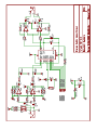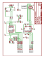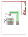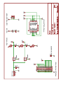
1
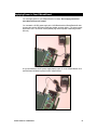
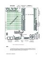
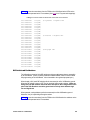
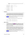
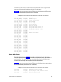
XStend Board V2.1 Manual
How to install and use
your new XStend Board
RELEASE DATE: 12/29/2002
Copyright ©1998-2003 by X Engineering Software Systems Corporation.
All XS-prefix product designations are trademarks of XESS Corp.
All XC-prefix product designations are trademarks of Xilinx.
All rights reserved. No part of this publication may be reproduced, stored in a retrieval
system, or transmitted, in any form or by any means, electronic, mechanical,
photocopying, recording, or otherwise, without the prior written permission of the publisher.
Printed in the United States of America.
XSTEND BOARD V2.1 USER MANUAL
1
Table of Contents
Table of Contents .............................................................................................2
Preliminaries .....................................................................................................4
Getting Help!.................................................................................................4
Take notice!! .................................................................................................4
Packing List ..................................................................................................4
Installation .........................................................................................................5
Inserting the XSA Board into an XStend Board..........................................5
Applying Power to Your XStend Board.......................................................6
Making Connections to Your XSA and XStend Boards............................7
Setting the Jumpers on Your XStend Board ..............................................8
Programmer's Models ......................................................................................9
XStend Board Capabilities...........................................................................9
XStend Board Components.......................................................................10
LEDs ...........................................................................................................11
DIP Switch and Pushbuttons.....................................................................12
RS-232 Port................................................................................................13
USB 1.1 Interface .......................................................................................13
SRAM..........................................................................................................14
IDE Interface...............................................................................................14
Stereo Audio Codec...................................................................................15
XSA Board Mounting Sockets...................................................................16
Daughterboard Connector .........................................................................16
Prototyping Area.........................................................................................16
Interactions Between the XSA Board and XStend Board Components .16
XSA Pushbutton Interactions.....................................................................17
XSTEND BOARD V2.1 USER MANUAL
2
XSA VGA Port Interactions........................................................................17
XSA DIP Switches......................................................................................17
XSA Flash RAM .........................................................................................17
XSA Seven-Segment LED ........................................................................17
XSA SDRAM ..............................................................................................17
XStend Codec ............................................................................................18
RS-232 Port................................................................................................18
USB Interface .............................................................................................18
XStend DIP Switch.....................................................................................18
XStend LEDs..............................................................................................19
XStend IDE Interface .................................................................................19
XStend SRAM ............................................................................................20
XStend + XSA Pin Connections.....................................................................21
XStend Schematics ........................................................................................22
XSTEND BOARD V2.1 USER MANUAL
3
1
Preliminaries
Getting Help!
Here are some places to get help if you encounter problems:
If you can't get the XStend Board hardware to work, submit a problem report at
http://www.xess.com/help.html. Our web site also has
answers to frequently-asked-questions,
example designs for the XS Boards,
application notes,
a place to sign-up for our email forum where you can post questions to other XS
Board users.
Take notice!!
The XStend Board V2.1 is not compatible with the XS95, XS40 or XSTE5 Boards! Do
not plug XS95, XS40 or XSTE5 Boards into the XStend Board V2.1!
If you are connecting a 9VDC power supply to your XStend Board, please make sure
the center terminal of the plug is positive and the outer sleeve is negative!
Packing List
Here is what you should have received in your package:
an XStend Board;
an XSTOOLs CDROM with software utilities and documentation for using the XStend
Board.
XSTEND BOARD V2.1 USER MANUAL
4
2
Installation
Inserting the XSA Board into an XStend Board
The XSA Board is inserted into the XStend Board as shown below. The XSA Board is
inserted into the inner-most columns of the socket strips. Orient the parallel port, VGA
port and PS/2 port connectors on the XSA Board as indicated on the XStend
Board!!
XSTEND BOARD V2.1 USER MANUAL
5
Applying Power to Your XStend Board
You can supply power to your XStend Board in four ways. Do not apply power from
more than one source at a time!!
You can attach a 9V DC power supply to the XSA Board and the XStend Board will draw
its power through the XSA Board prototyping header as shown below. (The power supply
should have a 2.1 mm female, center-positive plug and be capable of delivering at least
500 mA.)
Or you can attach the 9V DC power supply directly to jack J7 on the XStend Board. Now
the XSA Board will draw its power from the XStend Board.
XSTEND BOARD V2.1 USER MANUAL
6
You can also attach a standard ATX PC power supply to the XStend Board through
connector J6.
Finally, you can power the XStend Board from a dual 5V / 3.3V power supply directly to
binding posts on the XStend Board. (The binding posts are not provided.)
Making Connections to Your XSA and XStend Boards
You can make the same connections to your XSA Board whether it is inserted into the
XStend Board or used stand-alone. A 6' DB25 male-to-male cable attaches from the
parallel port on the PC to the female DB-25 connector (J8) at the top on the XSA Board.
You can connect a VGA monitor to the 15-pin connector (J3) at the bottom of your XSA
Board. And you can accept inputs from a keyboard or mouse by connecting it to the PS/2
connector (J4) at the bottom of your XSA Board.
XSTEND BOARD V2.1 USER MANUAL
7
The XStend Board offers some additional connection opportunities. You can connect the
peripheral end of a USB 1.1 cable to the USB port (J5) on the XStend Board while the
host end attaches to a PC USB port. You can perform serial communications by attaching
a 9-pin RS-232 null-modem cable between the DB9 connector (J9) on the XStend Board
and a serial port on a PC. You can capture audio output from a CD player or a
microphone by attaching them to the 3.5mm stereo input jack (J1) on the XStend Board,
while audio can be sent to a pair of headphones through the stereo output jack (J2).
Setting the Jumpers on Your XStend Board
The default jumper settings shown in Table 1 configure your XStend Board for use in a
logic design environment. You will need to change the jumper settings only if you are:
manually reseting the audio codec circuit,
accepting audio signals from a low-amplitude source (e.g., a passive microphone),
not using the USB interface.
• Table 1: Jumper settings for XSA Boards.
Jumper
Setting
Purpose
JP1
Off
(default)
Removing this shunt allows the audio codec to process stereo audio signals.
On
JP2
Off
(default)
On
JP3
JP4
Off
(default)
Removing this shunt sets the gain on the left stereo input channel to 48.
Off
Off
Off
On
(default)
JP12
Removing this shunt interrupts power to a passive microphone attached to the right stereo input
channel.
Off
On
(default)
JP11
Placing a shunt on this jumper provides power to a passive microphone attached to the left stereo
input channel.
Placing a shunt on this jumper provides power to a passive microphone attached to the right stereo
input channel.
On
(default)
JP10
Removing this shunt interrupts power to a passive microphone attached to the left stereo input
channel.
On
On
(default)
JP5
Placing a shunt on this jumper resets the audio codec and halts any input or output of stereo audio
signals.
Off
On
(default)
Placing a shunt on this jumper sets the gain on the left stereo input channel. to 1.
Removing this shunt sets the gain on the right stereo input channel to 48.
Placing a shunt on this jumper sets the gain on the right stereo input channel. to 1.
2
Removing this shunt disconnects the XSA Board from the I C data signal of the USB interface.
2
Placing a shunt on this jumper connects the XSA Board to the I C data signal of the USB interface.
2
Removing this shunt disconnects the XSA Board from the I C clock signal of the USB interface.
2
Placing a shunt on this jumper connects the XSA Board to the I C clock signal of the USB interface.
Removing this shunt disconnects the XSA Board from the clock output of the USB interface.
Placing a shunt on this jumper connects the XSA Board to the clock output of the USB interface.
XSTEND BOARD V2.1 USER MANUAL
8
3
Programmer's
Models
This section describes the various sections of the XStend Board and shows how the
prototyping header pins of the XSA Board are connected to the XStend Board circuitry.
Please refer to the complete schematics and pin list at the end of this document if you
need more details.
XStend Board Capabilities
The XSA Boards offer a flexible, low-cost method of prototyping FPGA designs. However,
their small physical size limits the amount of support circuitry they can hold. The XStend
Board removes this limitation by providing additional support circuitry that the XSA Boards
can access through their prototyping header interfaces.
The XStend Board contains resources that extend the range of applications of the XSA
Boards into these new areas:
The pushbuttons, DIP switches, LEDs, and prototyping area are useful for basic lab
experiments.
The static RAM can be used when the larger SDRAM on the XSA Board is overkill for
a particular application.
The stereo codec and dual-channel analog input/output circuitry are useful for
processing of audio signals in combination with DSP circuits synthesized for the
FPGA.
The USB 1.1 interface lets the XSA Board appear as a low-speed or full-speed USB
peripheral to a PC.
The RS-232 interface is useful when the XSA Board needs to send information over a
low-speed serial communication link.
The IDE interface provides the XSA Board with access to a hard disk for data storage
and retrieval.
XSTEND BOARD V2.1 USER MANUAL
9
XStend Board Components
The XStend Board extends the capabilities of the XSA Boards by providing:
additional bargraph LED and LED digits;
DIP switches and pushbuttons;
an RS-232 port;
a USB 1.1 peripheral interface;
an additional 128 Kbytes of static RAM;
an IDE interface to hard disks;
a stereo audio codec with left/right input and output channels;
mounting sockets for an XSA Board;
a 42×2 header connector for add-on daughterboards (optional);
a 2.75"×3.5" prototyping area with access to both the 3.3V or 5V supply.
These resources are shown in the simplified view of the XStend Board. Each of these
resources will be described in the following sections.
XSTEND BOARD V2.1 USER MANUAL
10
XSA Board
9V DC
Daughterboard
Mounting Sockets
Power Jack Connector
Pr
ot
IDE Hard Disk
Connector
ot
y
pi
n
g
A
re
a
ATX Power Supply
Connector
Power Supply
Binding Posts
10-Segment
LED Bargraph
Pushbuttons
Power Indicator
In
Out
Stereo Audio
Connectors
RS-232 Port
USB 1.1
Port
DIP Switch
7-Segment
LED Displays
• Figure 1: Simplified layout of the XStend Board.
LEDs
The XStend Board provides an XSA Board with a ten-segment bargraph LED and two
more LED seven-segment displays. All of these LEDs are active-high meaning that an
LED segment will glow when a high logic level is applied to it.
XSTEND BOARD V2.1 USER MANUAL
11
Listing 1 shows the connections from the FPGA on the XSA Board to the LEDs on the
XStend Board expressed as UCF constraints (click here for UCF syntax and usage tips).
• Listing 1: Connections between the XStend LEDs and the FPGA on the XSA Board.
net
net
net
net
net
net
net
net
net
net
net
net
net
net
net
net
net
net
net
net
net
net
net
net
net
net
ledtwo<0>
ledtwo<1>
ledtwo<2>
ledtwo<3>
ledtwo<4>
ledtwo<5>
ledtwo<6>
ledtwo<7>
ledone<0>
ledone<1>
ledone<2>
ledone<3>
ledone<4>
ledone<5>
ledone<6>
ledone<7>
barled<1>
barled<2>
barled<3>
barled<4>
barled<5>
barled<6>
barled<7>
barled<8>
barled<9>
barled<10>
loc=p47;
loc=p40;
loc=p28;
loc=p29;
loc=p27;
loc=p42;
loc=p48;
loc=p38;
loc=p64;
loc=p65;
loc=p76;
loc=p50;
loc=p51;
loc=p54;
loc=p56;
loc=p63;
loc=p68;
loc=p44;
loc=p46;
loc=p49;
loc=p57;
loc=p62;
loc=p60;
loc=p67;
loc=p39;
loc=p59;
# rightmost 7-segment LED
# leftmost 7-segment LED
# bargraph LED
DIP Switch and Pushbuttons
The XStend has a bank of eight DIP switches and three pushbuttons that are accessible
by an XSA Board. (There is a fourth pushbutton labeled PROG, which is used to initiate
the programming of the XSA Board. It is not intended to be a general-purpose input.)
When closed or ON, each DIP switch pulls the connected pin of the XS Board to ground.
When the DIP switch is open or OFF, the pin is pulled high through a resistor. When not
being used, the DIP switches should be left in the open or OFF configuration so the
pins of the XSA Board are not tied to ground and can freely move between logic
low and high levels.
When pressed, each pushbutton pulls the connected pin of the XS Board to ground.
Otherwise, the pin is pulled high through a resistor.
Listing 2 shows the connections from the FPGA on the XSA Board to the switches on the
XStend Board expressed as UCF constraints.
XSTEND BOARD V2.1 USER MANUAL
12
• Listing 2: Connections between the XStend DIP/pushbutton switches and the FPGA on the XSA
Board.
net
net
net
net
net
net
net
net
net
net
net
pushsw<3>
pushsw<4>
pushsw<5>
dipsw<1>
dipsw<2>
dipsw<3>
dipsw<4>
dipsw<5>
dipsw<6>
dipsw<7>
dipsw<8>
loc=p78;
loc=p26;
loc=p23;
loc=p30;
loc=p58;
loc=p74;
loc=p75;
loc=p66;
loc=p77;
loc=p80;
loc=p79;
# pushbuttons
# DIP switches
RS-232 Port
The XStend Board has a 9-pin RS-232 port that provides the XSA Board with the transmit
and receive serial data streams (TD and RD, respectively) as well as the flow control
signals (RTS and CTS, respectively). The pin functions on the XStend Board RS-232 port
are identical to those found on a PC serial port, so a null modem cable that swaps the
TD/RD and CTS/RTS lines is needed if the XStend Board and PC are to communicate.
Listing 3 shows the connections from the FPGA on the XSA Board to the RS-232 port
pisn on the XStend Board expressed as UCF constraints.
• Listing 3: Connections between the XStend RS-232 port and the FPGA on the XSA Board.
net
net
net
net
td
rd
rts
cts
loc=p83;
loc=p60;
loc=p80;
loc=p62;
#
#
#
#
RS232
RS232
RS232
RS232
TD port pin 3
RD port pin 2
RTS port pin 7
CTS port pin 8
USB 1.1 Interface
The XStend Board uses a Philips PDIUSBD11 USB-to-I2C interface chip to provide the
XSA Board with a USB communication link. The FPGA accesses registers on the chip
via the serial clock and data lines of the I2C link. By reading and writing these registers,
the FPGA can act as a USB peripheral with the USB interface chip handling the low-level
data transactions for the USB bus.
The USB interface chip also provides an interrupt signal to alert the FPGA when USB
tranactions need to be processed. In addition, a SUSPEND signal is also output from the
chip to alert the FPGA when the USB bus loses power or otherwise ceases operations.
Finally, a clock output from the chip is made available to the XSA Board on its external
clock input of the programmable oscillator. The frequency of this clock is 48 MHz / (N+1)
where N is a value loaded into a register on the chip through the I2C interface.
Listing 4 shows the connections from the FPGA on the XSA Board to the USB interface
chip on the XStend Board expressed as UCF constraints.
XSTEND BOARD V2.1 USER MANUAL
13
• Listing 4: Connections between the XStend USB interface chip and the FPGA on the XSA Board.
net
net
net
net
sda
scl
susp
intr
loc=p85;
loc=p84;
loc=p29;
loc=p28;
#
#
#
#
I2C data signal
I2C clock signal
SUSPEND signal
INTERRUPT signal
SRAM
The XStend Board gives the XSA Board access to a Cypress CY7C109 128 KByte
SRAM.
Listing 5 shows the connections from the XSA Board to the SRAM on the XStend Board
(expressed as UCF constraints):
• Listing 5: Connections between the XStend SRAM and the FPGA on the XSA Board.
net
net
net
net
net
net
net
net
net
net
net
net
net
net
net
net
net
net
net
net
net
net
net
net
net
net
net
net
ceb loc=p79;
oeb loc=p43;
web loc=p58;
a<0> loc=p27;
a<1> loc=p38;
a<2> loc=p66;
a<3> loc=p65;
a<4> loc=p64;
a<5> loc=p63;
a<6> loc=p56;
a<7> loc=p54;
a<8> loc=p42;
a<9> loc=p40;
a<10> loc=p28;
a<11> loc=p29;
a<12> loc=p51;
a<13> loc=p47;
a<14> loc=p50;
a<15> loc=p48;
a<16> loc=p39;
d<0> loc=p60;
d<1> loc=p62;
d<2> loc=p67;
d<3> loc=p57;
d<4> loc=p49;
d<5> loc=p46;
d<6> loc=p44;
d<7> loc=p68;
#
#
#
#
chip-enable (active-low)
output-enable (active-low)
write-enable (active-low)
address lines
# data lines
IDE Interface
The XStend Board provides the XSA Board with access to a hard disk through the IDE
interface connector. The FPGA stores and retrieves data from the disk by reading and
writing registers on the disk through the IDE interface. These registers are accessed
using the read and write strobes in combination with the register bank select lines, the
three-bit register address bus and the sixteen-bit IDE data bus.
XSTEND BOARD V2.1 USER MANUAL
14
In addition to polled access, the IDE interface also allows DMA access using the DMA
request and acknowledge signals along with the I/O ready signal.
Listing 6 shows the connections from the FPGA on the XSA Board to the IDE interface
chip on the XStend Board expressed as UCF constraints.
• Listing 6: Connections between the XStend IDE interface and the FPGA on the XSA Board.
net
net
net
net
net
net
net
net
net
net
net
net
net
net
net
net
net
net
net
net
net
net
net
net
net
net
net
net
ide_resetb
ide_dmarq
ide_dmackb
ide_intrq
ide_iordy
ide_diorb
ide_diowb
ide_cs0b
ide_cs1b
ide_da<0>
ide_da<1>
ide_da<2>
ide_d<0>
ide_d<1>
ide_d<2>
ide_d<3>
ide_d<4>
ide_d<5>
ide_d<6>
ide_d<7>
ide_d<8>
ide_d<9>
ide_d<10>
ide_d<11>
ide_d<12>
ide_d<13>
ide_d<14>
ide_d<15>
loc=p31;
loc=p27;
loc=p38;
loc=p40;
loc=p39;
loc=p86;
loc=p87;
loc=p54;
loc=p56;
loc=p64;
loc=p66;
loc=p63;
loc=p68;
loc=p44;
loc=p46;
loc=p49;
loc=p57;
loc=p62;
loc=p60;
loc=p67;
loc=p42;
loc=p43;
loc=p47;
loc=p48;
loc=p50;
loc=p51;
loc=p58;
loc=p65;
#
#
#
#
#
#
#
#
#
#
reset
DMA request
DMA acknowledge
interrupt
I/O ready
read strobe
write strobe
register bank select 0
register bank select 1
register address lines
# data I/O lines
Stereo Audio Codec
The XStend Board has an AK4551 stereo audio codec that accepts two analog input
channels, digitizes the analog values, and sends the digital values to the XSA Board as a
serial bit stream. The codec also accepts a serial bit stream from the XSA Board and
converts it into two analog output signals that exit the XStend Board.
Listing 7 shows the connections from the FPGA on the XSA Board to the codec interface
on the XStend Board (expressed as UCF constraints):
• Listing 7: Connections between the XStend stereo codec and the FPGA on the XSA Board.
net mclk
net lrck
net sclk
XSTEND BOARD V2.1 USER MANUAL
loc=p77;
loc=p59;
loc=p75;
# master clock to codec
# left/right codec chaneel select
# serial data clock
15
net sdin
net sdout
loc=p74;
loc=p76;
# serial data stream to codec
# serail data stream from codec
The analog stereo input and output signals enter and exit the XStend Board through the
3.5mm jacks J1 and J2, respectively. The output of an audio CD player can be input
through J1 and a set of small stereo headphones can be connected to J2 for listening to
the processed output. In addition, a passive microphone can be connected to J1 by
placing shunts on jumpers JP2 and JP3 and removing shunts from JP4 and JP5.
XSA Board Mounting Sockets
The XSA Board is mounted using the inner rows of the double-row sockets on the XStend
Board. These sockets connect the prototyping header of the XSA Board to the
components of the XStend Board.
In addition, the outer rows of each socket provide access points for probing the signals
that go through the sockets. Each hole in the outer rows is electrically connected to the
horizontally adjacent hole on the inner rows. Small wires (22-gauge or less) can be
inserted in the holes on the outer rows and logic or oscilloscope probes can be attached to
monitor the signals going through the mounting socket.
Daughterboard Connector
Daughterboards with specialized circuitry can be connected to the XStend board through
connector J4. This 42×2 connector brings all the I/O and VCC/GND from the XSA Board
to the daughterboard.
Prototyping Area
The XStend Board has a prototyping area consisting of component through-holes on an
0.1"×0.1" grid. Components in this area can access to the +5V, +3.3V and signal ground
by making connections to the appropriate pins on the JP9 header.
Connections from the XSA Board to the prototyping area are made through the
daughterboard header. Each pin on J4 is explicitly labeled with the corresponding number
of the FPGA pin it connects to on the XSA Board. For example, the pin at the bottom-left
of J4 on the XStend Board is connected to pin 111 of the FPGA on the XSA Board.
Interactions Between the XSA Board and XStend Board Components
Many of the FPGA pins on the XSA Board are connected to two or more components on
the XSA and/or XStend Board. This causes interactions that may make it difficult or
impossible to use these components in the same application. This section will provide an
overview of some of the possible interactions between the components. These
discussions are overly pessimistic in terms of what components cannot be used together
in a single application, so advanced users are encouraged to check the list of pin
assignments in Appendix A for more details.
XSTEND BOARD V2.1 USER MANUAL
16
XSA Pushbutton Interactions
The pushbutton on the XSA Board connects to the same FPGA pin as the data pin of the
XSA Board’s PS/2 port. These components cannot be used simultaneously.
XSA VGA Port Interactions
The horizontal and vertical sync signals of the XSA Board use the same FPGA pins as
two of the pushbuttons on the XStend Board (SW3 and SW4). These components cannot
be used simultaneously.
XSA DIP Switches
The DIP switch on the XSA Board shares FPGA pins with the XSA Board Flash RAM and
the XStend Board SRAM chip, seven-segment LED (LED1) and the IDE interface.
Therefore, the XSA Board DIP switches should be left in the OFF (OPEN) position if these
other components are being used.
XSA Flash RAM
The Flash RAM on the XSA Board shares FPGA pins with the XSA Board DIP switch,
seven-segment LED and CPLD parallel port interface, and with the XStend Board SRAM,
both seven-segment LEDs, bargraph LED, stereo audio codec, DIP switch, USB port and
IDE interface.
The Flash RAM and SRAM can be deselected using their respective chip-select signals,
so these components can be used simultaneously in an application. The IDE interface
can also be used at the same time as these other two components by activating its read or
write control signal only when the Flash RAM and SRAM are not selected.
The codec, DIP switches (on both the XSA and XStend Boards), LEDs (on both the XSA
and XStend Boards) and USB port do not have chip-selects. Therefore, these
components cannot be used in applications where the Flash RAM is needed.
The default parallel port interface programmed into the XSA Board CPLD will disable
outputs that interfere with the operations of the Flash RAM. Therefore, it can be used
without modification in applications that employ the Flash RAM.
XSA Seven-Segment LED
The seven-segment LED on the XSA Board shares FPGA pins with the XSA Board Flash
RAM and the XStend Board SRAM, bargraph LED, RS-232 port and IDE interface.
Therefore, these components cannot be used in applications where the seven-segment
LED on the XSA Board is needed.
XSA SDRAM
The synchronous DRAM chip on the XSA Board does not share any FPGA pins with any
other components. Therefore, any application can use the SDRAM regardless of the
other components that are to be used.
XSTEND BOARD V2.1 USER MANUAL
17
XStend Codec
The stereo audio codec on the XStend Board shares FPGA pins with the XSA Board
Flash RAM and the XStend Board bargraph LED, seven-segment LED (LED1), and DIP
switch. Therefore, these components cannot be used in applications where the codec is
needed.
RS-232 Port
The RS-232 port on the XStend Board shares FPGA pins with the XSA Board Flash RAM
and seven-segment LED, and with the XStend Board SRAM, DIP switch, bargraph LED
and IDE interface.
The Flash RAM, SRAM, and IDE interface can be deselected using their respective chipselect or read/write signals, so these components can be used simultaneously in an
application with the RS-232 port. The RS-232 port has resistors on its outputs that drive
the FPGA pins so these signals will be overridden by the Flash RAM, SRAM or IDE
signals when they are active.
The DIP switch and LEDs (on both the XSA and XStend Boards) do not have chip-selects.
Therefore, these components cannot be used in applications where the RS-232 port is
needed.
USB Interface
The USB interface on the XStend Board shares FPGA pins with the XSA Board Flash
RAM and the XStend Board SRAM and one seven-segment LED (LED2).
The Flash RAM and SRAM can be deselected using their respective chip-select signals,
so these components can be used simultaneously in an application with the USB
interface. The USB interface signals have resistors on the outputs that drive the FPGA
pins so these signals will be overridden by the Flash RAM or SRAM signals when they are
active.
The LED does not have a chip-select. Therefore, it cannot be used in applications where
the USB interface port is needed.
XStend DIP Switch
The DIP switch on the XStend Board shares FPGA pins with the XSA Board Flash RAM,
CPLD parallel port interface, and the /WRITE pin that controls configuration of the FPGA,
and with the XStend Board SRAM, stereo audio codec and IDE interface. Therefore, the
XStend Board DIP switches should be left in the OFF (OPEN) position if these other
components are being used.
If the XStend Board DIP switch is used, then the Flash RAM and SRAM should not be
enabled, and registers in the IDE interface should not be read or written. Position 1 of the
DIP switch should be in the OFF (OPEN) position so the /WRITE signal of the FPGA can
be controlled when the FPGA is being configured. There are resistors in the outputs of the
codec that drive the FPGA so these signals can be overridden if the DIP switch is used.
The CPLD on the XSA Board must also be programmed with the alternate parallel port
XSTEND BOARD V2.1 USER MANUAL
18
interface found in the XSA\dwnldpa2.svf file so it will not drive the pins of the FPGA that
are already being pulled low by the DIP switch.
XStend LEDs
The seven-segment LED1 on the XStend Board shares FPGA pins with the XSA Board
Flash RAM, CPLD parallel port interface and DIP switch, and with the XStend Board
SRAM, stereo audio codec and IDE interface. Therefore, these components cannot be
used in applications where the seven-segment LED1 on the XStend Board is needed.
The alternate parallel port interface found in the XSA\dwnldpa2.svf file must also be
programmed into the CPLD on the XSA Board so it does not drive the segments of LED1
when the FPGA tries to do so.
The seven-segment LED2 on the XStend Board shares FPGA pins with the XSA Board
Flash RAM, CPLD parallel port interface and DIP switch, and with the XStend Board
SRAM, USB interface and IDE interface. Therefore, these components cannot be used in
applications where the seven-segment LED2 on the XStend Board is needed. The
alternate parallel port interface found in the XSA\dwnldpa2.svf file must also be
programmed into the CPLD on the XSA Board so it does not drive the segments of LED2
when the FPGA tries to do so.
The bargraph LED on the XStend Board shares FPGA pins with the XSA Board Flash
RAM and seven-segment LED, and with the XStend Board SRAM, stereo audio codec,
RS-232 port, and IDE interface. Therefore, these components cannot be used in
applications where the bargraph LED on the XStend Board is needed.
XStend IDE Interface
The IDE interface on the XStend Board shares FPGA pins with the XSA Board Flash
RAM, seven-segment LED, CPLD parallel port interface and DIP switch, and with the
XStend Board SRAM, RS-232 port, bargraph and seven-segment LEDs, and DIP switch.
The Flash RAM and SRAM can be deselected using their respective chip-select signals,
so these components can be used simultaneously in an application with the IDE interface.
The IDE interface can also be used at the same time as these other two components by
activating its read or write control signal only when the Flash RAM and SRAM are
deselected.
The DIP switches and LEDs (on both the XSA and XStend Boards) do not have chipselects. Therefore, these components cannot be used in applications where the IDE
interface is needed.
The RS-232 port has resistors on its outputs that drive the FPGA pins so these signals will
be overridden by the IDE signals when they are active. So the RS-232 port and IDE
interface can both be used in the same application.
The alternate parallel port interface found in the XSA\dwnldpa2.svf file must also be
programmed into the CPLD on the XSA Board so it does not drive the pins of the FPGA
that are already being driven through the IDE interface.
XSTEND BOARD V2.1 USER MANUAL
19
XStend SRAM
The SRAM on the XStend Board shares FPGA pins with the XSA Board Flash RAM,
seven-segment LED, CPLD parallel port interface and DIP switch, and with the XStend
Board RS-232 port, bargraph and seven-segment LEDs, DIP switch, USB interface and
IDE interface.
The Flash RAM and IDE interface can be deselected using their respective chip-select or
read/write signals, so these components can be used simultaneously in an application with
the SRAM.
The DIP switches and LEDs (on both the XSA and XStend Boards) do not have chipselects. Therefore, these components cannot be used in applications where the SRAM is
needed.
The RS-232 port and USB interface both have resistors on their outputs that drive the
FPGA pins so these signals will be overridden by the SRAM signals when they are active.
So the RS-232 port, USB interface and IDE interface can all be used in the same
application.
The alternate parallel port interface found in the XSA\dwnldpa2.svf file must also be
programmed into the CPLD on the XSA Board so it does not drive the pins of the FPGA
that are already being driven on the SRAM.
XSTEND BOARD V2.1 USER MANUAL
20
A
XStend + XSA Pin
Connections
The following table lists the connections between the XStend Board components and the
components of the XSA Board. The columns of the table are arranged as follows:
Column 1 lists the Spartan-II FPGA pin. It is left blank if there is no connection to the
FPGA for this function. Pins marked with * are useable as general-purpose I/O
through the prototyping header; pins denoted with ** can be used as general-purpose
I/O only if the CPLD interface is reprogrammed with the alternate parallel port
interface stored in the dwnldpa2.svf file; pins with no marking cannot be used as
general-purpose I/O at all.
Column 2 lists the XC9572XL CPLD pin. It is left blank if there is no connection to the
CPLD for this function.
Column 3 lists the pins of other devices on the XSA Board that are connected to the
associated FPGA and/or CPLD pin.
Column 4 lists the pin of the XSA prototyping header that is connected to the associated
FPGA and/or CPLD pin.
Columns 5–7 list the pins of devices on the Xstend Board that will connect to the FPGA
and/or CPLD when the XSA Board is inserted into an Xstend Board.
XSTEND BOARD V2.1 USER MANUAL
21
FPGA
1
2
3
4
5
6
7
8
9
10
11
12*
13*
15*
18*
19*
20*
21*
22*
23*
26*
27*
28*
29*
30*
31*
32
34
37
38*
39*
40*
41*
42**
43**
44*
46*
47**
48**
49*
50**
51**
54*
56*
57*
58**
59*
60*
62*
63*
64*
65**
66*
67*
68*
69
72
74*
75*
76*
77*
78*
79*
80*
PARPORT-S6
CPLD XSA Function
+3.3V
13
SPARTAN-TCK
SDRAM-A7
SDRAM-A1
SDRAM-A6
SDRAM-A2
SDRAM-A5
GND
+2.5V
SDRAM-A3
SDRAM-A4
VGA-RED0
VGA-RED1
SPARTAN-GCK3
SPARTAN-GCK2
VGA-GREEN0
VGA-GREEN1
VGA-BLUE0
VGA-BLUE1
VGA-/HSYNC
VGA-/VSYNC
62
FLASH-A3
63
FLASH-A2, *PARPORT-S5
64
FLASH-A1, *PARPORT-S4
19
SPARTAN-/WRITE
15
SPARTAN-CS
15*
SPARTAN-TDI
19*
SPARTAN-TDO
16
SPARTAN-CCLK
18
SPARTAN-DOUT/BSY
2
FLASH-D0,DIN/D0,LED-S1
1
FLASH-A0, *PARPORT-S3
11
FLASH-/CE
57
FLASH-A10, *PARPORT-D2
12
FLASH-/OE, *PARPORT-D7
4
FLASH-D1,LED-DP
5
FLASH-D2,LED-S4
43
FLASH-A11, *PARPORT-D3
44
FLASH-A9, *PARPORT-D1
6
FLASH-D3,LED-S6
45
FLASH-A8, *PARPORT-D0
46
FLASH-A13, *PARPORT-D5
47
FLASH-A14,DIPSW1A
48
FLASH-A17,DIPSW1D
7
FLASH-D4,LED-S5
49
FLASH-/WE, *PARPORT-D6
50
FLASH-/RESET
8
FLASH-D5,LED-S3
9
FLASH-D6,LED-S2
51
FLASH-A16,DIPSW1C
52
FLASH-A15,DIPSW1B
56
FLASH-A12, *PARPORT-D4
58
FLASH-A7
10
FLASH-D7,LED-S0
38
SPARTAN-/INIT
39
SPARTAN-/PROGRAM
40
SPARTAN-DONE
61
FLASH-A4
60
FLASH-A5
59
FLASH-A6
27
28
31
1
29
32
33
34
36
37
50
51
56
69
68
15
30
73
45
71
57
65
58
61
40
39
59
60
38
78
79
82
83
35
62
66
80
81
84
3
4
5
10
41
55
53
70
77
6
9
67
7
8
52
22
Proto. Pin
54
16
/RAM_CE
AUDIO_SDTI
AUDIO_SCLK
AUDIO_SDTO
AUDIO_MCLK
LED2-F
RAM-A8
/RAM-OE
RAM-D6
RAM-D5
RAM-A13
RAM-A15
RAM-D4
RAM-A14
RAM-A12
RAM-A7
RAM-A6
RAM-D3
/RAM-WE
AUDIO_LRCK
RAM-D0
RAM-D1
RAM-A5
RAM-A4
RAM-A3
RAM-A2
RAM-D2
RAM-D7
DIPSW3
DIPSW4
LED1-E
DIPSW6
PUSHB2
DIPSW8
DIPSW7
BARLED-2
BARLED-3
LED2-D
LED2-A
BARLED-4
LED1-G
LED1-B
LED1-F
LED1-A
BARLED-5
DIPSW2
BARLED-10
BARLED-7
BARLED-6
LED1-DP
LED1-D
LED1-C
DIPSW5
BARLED-8
BARLED-1
PUSHB1
LED2-DP
BARLED-9
LED2-C
PUSHB4
PUSHB3
LED2-B
LED2-E
LED2-G
DIPSW1
RS232_RTS
IDE_D6,RS232_RD
IDE_D5, RS232_CTS
IDE_DA2
IDE_DA0
IDE_D15
IDE_DA1
IDE_D7
IDE_D0
IDE_D8
IDE_D9
IDE_D1
IDE_D2
IDE_D10
IDE_D11
IDE_D3
IDE_D12
IDE_D13
/IDE_CS0
/IDE_CS1
IDE_D4
IDE_D14
/IDE_DMACK
IDE_IORDY
IDE_INTRQ
/IDE_RESET
IDE_DMARQ
/USB_INT
USB_SUSPEND
XST-2.x Functions
RAM-A1
RAM-A16
RAM-A9
RAM-A0
RAM-A10
RAM-A11
GND
+3.3V
FPGA
83*
84*
85*
86*
87*
88
91
93*
94*
95
96
99
100
101
102
103
106
109
111
112
113
114
115
116
117
118
120
121
122
123
124
126
129
130
131
132
133
134
136
137
138
139
140
141
142
18*
30
29
28
33
32
31
27
25
24
23
22
34
20
35
53
17
36
42
MASTER_CLK
SDRAM-CLK
PS2-DATA,PUSHBUTTON
PS2-CLK
SDRAM-Q0
SDRAM-Q15
SDRAM-Q1
SDRAM-Q14
SDRAM-Q2
SDRAM-Q13
SDRAM-Q3
SPARTAN-M2
SPARTAN-M0
SPARTAN-M1
SDRAM-Q12
SDRAM-Q4
SDRAM-Q11
SDRAM-Q5
SDRAM-Q10
SDRAM-Q6
SDRAM-Q9
SDRAM-Q7
SDRAM-Q8
SDRAM-QML
SDRAM-/WE
SDRAM-QMH
SDRAM-/CAS
SDRAM-CLK
SDRAM-/RAS
SDRAM-CKE
SDRAM-/CS
SDRAM-A12
SDRAM-BA0
SDRAM-A11
SDRAM-BA1
SDRAM-A9
SDRAM-A10
SDRAM-A8
SDRAM-A0
SPARTAN-TMS
PARPORT-C1,CPLD-TCK
PARPORT-C2,CPLD-TMS
PARPORT-C3,CPLD-TDI
PARPORT-D0
PARPORT-D1
PARPORT-D2
PARPORT-D3
PARPORT-D4
PARPORT-D5
PARPORT-D6
PARPORT-D7
PARPORT-S3
PARPORT-S4
PARPORT-S5
PARPORT-S7,CPLD-TDO
PROG-OSC
CPLD XSA Function
64
17
12
14
21
25
26
Proto. Pin
18
19
20
23
24
13
Osc-In
MASTER_CLK
USB_CLKOUT
XST-2.x Functions
RS232_TD
USB_SCL
USB_SDA
/IDE_DIOR
/IDE_DIOW
B
XStend Schematics
The following pages show the detailed schematics for the XStend Board.
XSTEND BOARD V2.1 USER MANUAL
22