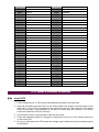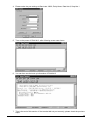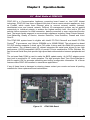
1
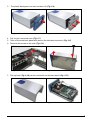
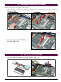
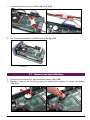
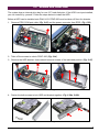
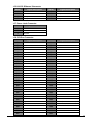
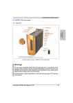
PNA-2413
Communications Appliance
User′s Manual
Revision: 010
Por twell Inc.
3F, No. 92, Sec. 1, Nei-Hu Rd., Taipei 114, Taiwan, R.O.C.
Headquarter: +886-2-2799-2020 FAX: +886-2-2799-1010
http://www.portwell.com.tw
Email: [email protected]
Item NO: B8980670
Table of Contents
Chapter 1
Chapter 2
Introduction ......................................................................................................... 2
1.1
About This Manual ......................................................................................... 2
1.2
Manual Organization ...................................................................................... 2
1.3
Technical Support Information........................................................................ 2
Getting Started .................................................................................................... 3
2.1
Included Hardware ......................................................................................... 3
2.2
Before You Begin ........................................................................................... 3
2.3
The Chassis ................................................................................................... 4
2.4
Opening the Chassis ...................................................................................... 4
2.5
Installing or Removing a SODIMM.................................................................. 6
2.6
Remove and Install DOM ............................................................................... 6
2.7
Remove and Install Battery............................................................................. 7
2.8
Remove and Install HDD ................................................................................ 8
2.9
Remove and Install PCI card........................................................................ 10
2.10 Product Specifications.................................................................................. 12
2.11 Hardware Configuration Setting.................................................................... 13
2.12 Install a Different Processor.......................................................................... 18
2.13 Use a Client Computer ................................................................................. 19
Chapter 3
Operation Guide................................................................................................ 21
3.1
Brief Guide of PPAP-200.............................................................................. 21
3.2
System Architecture ..................................................................................... 22
PNC-2413 User’s Manual
1
Chapter 1
Introduction
1.1 About This Manual
This manual describes all required information for setting up and using the PNA-2413.
PNA-2413 provides the essential components for delivering optimal performance and
functionality in the value communications appliance market segment. This manual should
familiarize you with PNA-2413 operations and functions. PNA-2413 has three on-board LAN
ports to serve communication appliances, such as Firewall, which needs three LAN ports to
connect external network (internet), demilitarized zone and internal network.
Feature of PNA-2413 includes:
u
Versatile networking and I/O capabilities: 3 Ethernet ports
u
Two USB ports
u
One COM port
u
Up to 256 Mbyte of SODIMM memory
u
One on-board DMA/33/66/100 IDE channel to support up to four IDE devices
u
One PCI right-angle connector for ease of connectivity to the PCI bus
1.2 Manual Organization
The manual describes how to configure your PNA-2413system to meet various operating
requirements. It is divided into three chapters, with each chapter addressing a basic concept
and operation of this whole system.
Chapter 1:
Introduction. This section briefly talks about how this document is organized. It includes
some guidelines for users who do not want to read through everything, but still helps
you find what you need.
Chapter 2:
Hardware Configuration Setting and Installation. This chapter shows how the hardware
is put together, including detailed information. It shows the definitions and locations of
Jumpers and Connectors that you can easily configure your system. Descriptions on
how to properly mount the CPU and main memory are also included to help you get a
safe installation. Reading this chapter will teach you how to set up PNA-2413.
Chapter 3:
Operation Information. This section gives you illustrations and more information on the
system architecture and how its performance can be maximized.
Any updates to this manual, technical clarification and answers to frequently asked questions
would be posted on the web site: http://isc.portwell.com.tw
1.3 Technical Support Information
Users may find helpful tips or related information on Portwell's web site: http://www.portwell.com.tw.
A direct contact to Portwell's technical person is also available. For further support, users may
also contact Portwell’s headquarter in Taipei or your local distributors.
Taipei Office Phone Number: +886-2-27992020
PNC-2413 User’s Manual
2
Chapter 2
Getting Started
This section describes how the hardware installation and system settings should be done.
2.1 Included Hardware
The following hardware is included in your kit:
u
PPAP-200 Communication Appliance System Board
u
AC to 15V DC adapter
u
One null serial port cable
2.2 Before You Begin
To prevent damage to any system board, it is important to handle it with care. The following
measures are generally sufficient to protect your equipment from static electricity discharge:
When handling the board, use a grounded wrist strap designed for static discharge elimination
and touch a grounded metal object before removing the board from the antistatic bag. Handle
the board by its edges only; do not touch its components, peripheral chips, memory modules or
gold contacts.
When handling processor chips or memory modules, avoid touching their pins or gold edge
fingers. Put the value communications appliance system board and peripherals back into the
antistatic bag when they are not in use or not installed in the chassis.
Some circuitry on the system board can continue operating even though the power is switched
off. Under no circumstances should the Lithium coin cell used to power the real-time clock be
allowed to be shorted. The coin cell can heat under these conditions and present a burn hazard.
Warning:
1.
"CAUTION: DANGER OF EXPLOSION IF BATTERY IS INCORRECTLY
REPLACED. REPLACE ONLY WITH SAME OR EQUIVALENT TYPE
RECOMMENDED BY THE MANUFACTURER. DISCARD USED BATTERIES
ACCORDING TO THE MANUFACTURER’S INSTRUCTIONS"
2.
This guide is for technically qualified personnel who have experience installing
and configuring system boards Disconnect the system board power supply
from its power source before you connect/disconnect cables or install/remove
any system board components. Failure to do this can result in personnel injury
or equipment damage.
3.
Avoid short-circuiting the lithium battery; this can cause it to superheat and
cause burns if touched.
4.
Do not operate the processor without a thermal solution. Damage to the
processor can occur in seconds.
5.
Do not block air vents. Minimum 1/2-inch clearance required.
PNC-2413 User’s Manual
3
2.3 The Chassis
The system is integrated in a customized 2U chassis (Fig. 2-1, Fig. 2-2). On the front panel you
will find an 4-push-button LCD module (EZIO). The back panel has three LAN ports, two USB
ports and a COM port.
Fig. 2-1 Front View of the Chassis
Fig. 2-2 Rear View of the Chassis
2.4 Opening the Chassis
1. Remove both bolts from the serial port (Fig. 2-3) and then take off the screws to loose back
panel (Fig. 2-4).
Fig. 2-3 Remove bolts from COM port
Fig. 2-4 Take off the screws on back panel
2. Turn PNA-2413 over. Press both metal
clips hard to loose the plastic back cover
(Fig. 2-5).
Fig. 2-5 Press the metal clips on the bottom
PNC-2413 User’s Manual
4
3.
The plastic back panel can then be taken off (Fig. 2-6).
Fig. 2-6 Take off the plastic back panel
Fig. 2-7 Pull out the inner steel case
4. Pull out the inner steel case (Fig. 2-7).
5. Take off the steel back panel and remove the indicated connector ( Fig. 2-8).
6. Remove the screws on the side (Fig. 2-9).
Fig. 2-8 Take off the steel back panel
Fig. 2-9 Remove the screws on the side
7. The top lead (Fig. 2-10) can be removed from the base stand (Fig. 2-11).
Fig. 2-10 The top lead
PNC-2413 User’s Manual
Fig. 2-11 The base stand
5
2.5 Installing or Removing a SODIMM
Follow these steps to upgrade RAM module:
1. Install the system memory by pulling the socket’s arm and pressing it into the slot gently.
(Fig. 2-12, 2-13)
Fig. 2-12 The memory slot
Fig. 2-13 Install SODIMM
2. By pulling the arms, the SODIMM can
eject itself (Fig. 2-14).
Fig. 2-14 Eject a SODIMM module
2.6 Remove and Install DOM
1. Insert the DOM (Fig. 2-16) into the IDE interface (Fig. 2-17).
Fig. 2-15 DiskOnModule
PNC-2413 User’s Manual
Fig. 2-16 Insert DOM into IDE interface
6
1. Connect the power source to DOM (Fig. 2-17, 2-18).
Fig. 2-17 Connect power to DOM
Fig. 2-18 DOM power connection
2. The completed installation of DOM is shown as Fig. 2-19.
Fig. 2-19 Completion of DOM power
connection
2.7 Remove and Install Battery
1. Press the metal clip back to eject the button battery (Fig. 2-20).
2. Replace it with a new one by pressing the battery with fingertip to restore the battery
(Fig. 2-21).
Fig. 2-20 Eject the battery
PNC-2413 User’s Manual
Fig. 2-21 Restore the battery
7
2.8 Remove and Install HDD
The system has an internal drive bay for one 3.5" hard disk drive. If the HDD is not pre-installed,
you can install it by yourself. Follow the steps below to install the HDD:
Before a HDD can be installed onto PNA-2413. PPAP-200 must be taken off from the chassis.
1. Remove EZIO COM port cable (Fig. 2-22) and the power connector from EZIO (Fig. 2-23).
Fig. 2-22 Remove the COM port cable
Fig. 2-23 Remove power connector from EZIO
2. Take off the screws to unlock PPAP-200 (Fig. 2-24).
3. Remove the HDD bracket. Users should remove screws of the indicated position (Fig. 2-25).
Fig. 2-24 Unscrew to loose PPAP-200
Fig. 2-25 Remove HDD bracket
4. Fasten the both screws to lock HDD and bracket together ( Fig. 2-26a, 2-26b).
Fig. 2-26a A 3.5” HDD and the HDD bracket
PNC-2413 User’s Manual
Fig. 2-26b Fix HDD to the bracket
8
5. Connect the IDE cable and power connector to HDD (Fig. 2-27).
6. Fasten both screws back to lock HDD onto chassis (Fig. 2-28).
Fig. 2-27 Connect power and IDE cable to
HDD
Fig. 2-28 Install into chassis
7. Fold the IDE cable under the hard disk in 45
interface connector (Fig. 2-29).
8. Put the PPAP-200 back to the chassis (Fig. 2-30).
Fig. 2-29 Fold the IDE cable
Fig. 2-30 Drive all four screws back
9. Connect the EZIO COM port cable and the IDE cable (Fig. 2-31).
Fig. 2-31 Recover cable connection
PNC-2413 User’s Manual
9
2.9 Remove and Install PCI card
One PCI slot is available to PNA-2413. Follow the steps below for installation:
1. The PCI slot is located on the back of the board ( Fig. 2-32).
2. The back of the PCI card should be against the back of PPAP-200 (Fig. 2-33, 2-34).
Fig. 2-32 PCI slot on the back of PPAP-200
Fig. 2-33 Push the PCI add-on card into the slot
3. Fix the board back in position with four screws (Fig. 2-35).
Fig. 2-34 The PCI card
Fig. 2-35 Reinstall after adding a PCI card
4. The metal tip of the PCI card’s bracket should be placed outside of the chassis corner (Fig. 2-36).
5. Plug the EZIO-COM port cable to both ends (Fig. 2-37).
Fig. 2-36 The PCI card’s bracket tip is placed
outside of the chassis corner
PNC-2413 User’s Manual
Fig. 2-37 Plug the EZIO COM port connector
to COM port
10
6. If there is an add-on PCI card, the original metal bracket needs to be removed ( Fig. 2-38).
7. Apply downward force (Fig. 2-39 ¬) and then slide toward the front panel (Fig. 2-39 Á). After
the cover is well tightly fit, put all four screws back to lock the top lead in position
(Fig. 2-39 Â).
¬
Á
Â
Fig. 2-38 Remove the original metal bracket
Fig. 2-39 Place the top cover back to the unit
8. Put the steel back panel back to the system and lock the PCI card in position by a screw.
(Fig. 2-40)
9. Push the back panel till it clips (Fig. 2-41 ¬). Then place both COM port bolts back (Fig. 2-41 Á).
¬
Á
Fig. 2-40 Fix the PCI card to the back panel
Fig. 2-41 Place the back panel in position
10. To finish up installation, drive two screws to lock up the back panel to chassis (Fig. 2-42).
Fig. 2-42 Lock the back panel
PNC-2413 User’s Manual
Fig. 2-43 Jumper Position
11
2.10 Product Specifications
Model:
PNA-2413
Main Processor:
•
Intel® socket 370 FC-PGA Celeron® /Pentium® III processors
(66, 100 or 133MHz system bus)
BIOS:
•
Award system BIOS with 512KB flash ROM to support DMI,
PnP, APM function
Main Memory:
•
One 144-pin SODIMM socket supports up to 512MB of 3.3V
SODIMM
L2 Cache Memory:
•
128KB/256KB PBSRAM built in (Celeron/Pentium III) CPU
module
Chipset:
•
Intel® 815E
PCI IDE Interface:
•
One 3.5” hard disk bay for DMA/33/66/100 IDE hard disk
Serial Ports:
•
•
Support two high-speed 16C550 compatible UARTs with 16-byte
T/R FIFOs
(Optional) Support LCD/Key pad module (Portwell proprietary)
USB Interface:
•
Support two USB ports for high speed I/O peripheral devices
Auxiliary I/O Interfaces:
•
System reset switch, power okay LED, Ethernet activity LED,
Ethernet speed LED, general purpose LED, alert LED and HDD
LED interface
Power Input:
•
Support one DC input jack (power requirement: DC 15V, 4.6A)
PCI Slot:
•
One PCI slot for add-on PCI card
On-board Ethernet:
•
Two Intel® 82559ER 10/100 Base-T fast Ethernet controller with
RJ-45 interface
One Intel® 82801BA (Internal MAC) + 82562ET (PHY) 10/100
Base-T fast Ethernet controller with RJ-45 interface
•
Main Memory:
•
Hardware Monitor:
Support on-board hardware monitor for
• CPU fan x 1
• Chassis fan x 2
• System voltages: Vcore, 3.3V, 1.8V, +5V and +12V
Power Good:
•
On-board power good interval: 140ms ~ 300ms; typical 200ms
Environmental
Requirements:
•
•
Operating Temperature: 5°C ~ 45°C
Storage Temperature: 5°C ~ 70°C
Relative Humidity: 5% ~ 95%, non-condensing
•
5.12"(L) x 8.5"(W)
Dimension:
PNC-2413 User’s Manual
•
One 144-pin SODIMM socket supports up to 512MB of 3.3V
SODIMM
12
2.11 Hardware Configuration Setting
This section gives the definitions and shows the positions of jumpers, headers and connectors.
All of the configuration jumpers on PPAP-200 are in the proper position. The default settings set
by factory are marked with a star ( ★ ).
Jumpers
In general, jumpers on PPAP-200 system board are used to select options for certain
features. Some of the jumpers are configurable for system enhancement. The others are
for testing purpose only and should not be altered. To select any option, cover the jumper
cap over (Short) or remove (NC) it from the jumper pins according to the following
instructions. Here NC stands for “Not Connected”. (Please refer to Fig. 2-43 for detailed
jumper positions.)
Jumper Setting Table (JP1/JP2/JP3)
JP1
Clear CMOS RAM
★
1-2
Normal
2-3
Clear CMOS RAM
JP2
CPU Frequency Strapping Default Setting
Short
N/C
N/C
Default Setting
Force CPU Frequency to safe mode
Use CPU Frequency strapping in ICH2 Register
JP3
Short
Default Setting
FWH Top Block Lock
Top Block Unlock
★
Default Setting
★
Top Block Lock
PNC-2413 User’s Manual
13
Connectors
Devices are connected through these connectors which includes IDE, COM Port etc…
Connector
Function
Remark
J1
Serial ports connector
J2
Reset push button
J3
FDC connector
J4
Secondary IDE connector
J5
Primary IDE connector
J6
Parallel port connector
J7
Chassis fan connector
J8
Chassis fan connector
J9
Serial ports connector
D-SUB 9
J10
Power output connector
Supply power to
IDE/FDC Interface
J11
Dual USB port connector
J12
VGA board connector
J13
Ethernet connector
J14
Ethernet connector
J15
Ethernet connector
J16
CPU fan
J17
Power jack
J18
Right angle PCI bus connector
Shrouded pin header
Need a CRT module
for VGA display
Pin Assignments of Connectors
J1/J9: Serial Port Connector
PIN No.
Signal Description
J2: Reset Push Button (Momentary)
PIN No.
Signal Description
1
DCD
1
Reset signal
2
RXD
2
Ground
3
TXD
4
DTR
5
SGND
6
DSR
7
RTS
8
CTS
9
RI
10
N/C (J1 only)
PNC-2413 User’s Manual
14
J3: FDC Connector
PIN No.
Signal Description
1
3
Ground
PIN No.
Signal Description
Density0#
Ground
2
4
5
Ground
6
Density1#
7
Ground
8
INDEX#
9
Ground
10
MOA#
11
Ground
12
DSB#
13
Ground
14
DSA#
15
Ground
16
MOB#
17
Ground
18
DIR#
19
Ground
20
STEP#
21
Ground
22
WD#
23
25
27
29
31
33
Ground
24
26
28
30
32
34
WE#
Ground
Ground
N/C
Ground
N/C
N/C
TRACK0#
WP#
RDATA#
HEAD#
DSKCHG#
J4/J5: IDE Connector
PIN No.
Signal Description
1
3
RESET#
PIN No.
Signal Description
Ground
Data 7
2
4
5
Data 6
6
Data 9
7
Data 5
8
Data 10
9
Data 4
10
Data 11
11
Data 3
12
Data 12
13
Data 2
14
Data 13
15
Data 1
16
Data 14
17
Data 0
18
Data 15
19
Ground
20
+5V
21
DMAREQ
22
Ground
23
25
27
29
31
33
35
37
39
IOW#
24
26
28
30
32
34
36
38
40
Ground
IOR#
IOCHRDY
DMAACK#
IRQ15/14
SA1
SA0
HDCCSO#
HDDACTIVE#
PNC-2413 User’s Manual
Data 8
Ground
Ground
Ground
N/C
PDIAG#1CSEL
SA2
HDCCS1#
Ground
15
J6: Parallel Connector
PIN No.
Signal Description
1
2
Strobe#
PIN No.
Signal Description
AFD#
Data 0
14
15
3
Data 1
16
INIT#
4
Data 2
17
SLIN#
5
Data 3
18
Ground
6
Data 4
19
Ground
7
Data 5
20
Ground
8
Data 6
21
Ground
9
Data 7
22
Ground
10
ACK#
23
Ground
11
BUSY
24
Ground
12
13
PE
25
26
Ground
SLCT
J7/J8/J16: Fan Connector
PIN No.
ERR#
N/C
J10 : Power Output Connector (To
provide IDE, FDC Interface power)
PIN No.
Signal Description
Signal Description
1
Ground
1
+12V
2
+12V
2
Ground
3
TachoMeter Signal
3
Ground
4
+5V
J11: Dual USB Port Connector
PIN No.
Signal Description
1
2
+5V
PIN No.
Signal Description
+5V
USBD0-
5
6
3
USBD0+
7
USBD0+
4
Ground
8
Ground
USBD0-
J12: VGA Connector
PIN No.
1
3
5
7
9
11
Signal Description
VID_RED
VID_GREEN
VID_BLUE
Ground
3VDDCCL
CRT_VSYNC
PNC-2413 User’s Manual
PIN No.
2
4
6
8
10
12
Signal Description
Ground
+1.8V
Ground
3VDDCDA
CRT_HSYNC
+5V
16
J13/J14/J15: Ethernet Connector
PIN No.
1
3
5
7
Signal Description
TX+
RX+
Termplane
Termplane
PIN No.
2
4
6
8
Signal Description
TXTermplane
RXTermplane
J17: Power Jack Connector
PIN No.
1
2
3
Signal Description
+15V
Ground
Ground
J18: PCI Bus Connector
PIN No.
B1
B2
B3
B4
B5
B6
B7
B8
B9
B10
B11
B12
B13
B14
B15
B16
B17
B18
B19
B20
B21
B22
B23
B24
B25
B26
B27
B28
B29
B30
B31
Signal Description
N/C
PTCK
Ground
N/C
+5V
+5V
PIRQ#C
PIRQ#A
N/C
N/C
N/C
Ground
Ground
N/C
Ground
PCICLK
Ground
PREQ#0
+5V
AD31
AD29
Ground
AD27
AD25
N/C
C_BE#3
AD23
Ground
AD21
AD19
N/C
PNC-2413 User’s Manual
PIN No.
A1
A2
A3
A4
A5
A6
A7
A8
A9
A10
A11
A12
A13
A14
A15
A16
A17
A18
A19
A20
A21
A22
A23
A24
A25
A26
A27
A28
A29
A30
A31
Signal Description
PTRST#
+12V
PTMS
PTDI
+5V
PIRQ#B
PIRQ#D
+5V
N/C
+5V
N/C
Ground
Ground
N/C
PCIRST#
+5V
PGNT#0
Ground
N/C
AD30
N/C
AD28
AD26
Ground
AD24
IDSEL (Connected to AD31)
N/C
AD22
AD20
Ground
AD18
17
B32
B33
B34
B35
B36
B37
B38
B39
B40
B41
B42
B43
B44
B45
B46
B47
B48
B49
B52
B53
B54
B55
B56
B57
B58
B59
B60
B61
B62
AD17
C_BE#2
Ground
IRDY#
N/C
DEVSEL#
Ground
PLOCK#
PERR#
N/C
SERR#
N/C
C_BE#1
AD14
Ground
AD12
AD10
Ground
A32
A33
A34
A35
A36
A37
A38
A39
A40
A41
A42
A43
A44
A45
A46
A47
A48
A49
AD16
N/C
FRAME#
Ground
TRDY#
Ground
STOP#
N/C
SDONE
SBO#
Ground
PAR
AD15
N/C
AD13
AD11
Ground
AD9
KEY
KEY
KEY
KEY
AD8
AD7
N/C
AD5
AD3
Ground
AD1
+5V
ACK64#
+5V
+5V
A52
A53
A54
A55
A56
A57
A58
A59
A60
A61
A62
C_BE#0
N/C
AD6
AD4
Ground
AD2
AD0
+5V
REQ64#
+5V
+5V
2.12 Install a Different Processor
Install CPU
1. Lift the handling lever of CPU socket outwards and upwards to the other end.
2. Align the processor pins with holes on the socket. Make sure that the notched corner or dot
mark (pin 1) of the CPU corresponds to the socket's bevel end. Then press the CPU gently
until it fits into place. If this operation is not easy or smooth, don't do it forcibly. You need to
check and rebuild the CPU pin uniformly.
3. Push down the lever to lock processor chip into the socket.
4. Follow the installation guide of cooling fan or heat sink to mount it on CPU surface and lock it
on the socket 370.
5. Be sure to follow particular CPU speed and voltage type to adjust the jumper settings properly
for all boards.
PNC-2413 User’s Manual
18
Remove CPU
1. Unlock the cooling fan first.
2. Lift the lever of CPU socket outwards and upwards to the other end.
3. Carefully lift up the existing CPU to remove it from the socket.
4. Follow the steps of CPU installation to change to another one or place handling bar to close
the opened socket.
Configure Processor Speed
The system was designed to self-detect its CPU speed. So it does not require any system
adjustment.
2.13 Use a Client Computer
Connection Using Hyper Terminal
If users use a headless PNA-2413, which has no mouse/keyboard and VGA output
connected to it, the console may be used to communicate with PNA-2413.
To access PNA-2413 via the console, Hyper Terminal is one of the choices. Follow the
steps below for the setup:
1. Execute HyperTerminal under C:\Program Files\Accessories\HyperTerminal
2. Enter a name to create new dial
3. For the connection settings, make it Direct to Com1.
PNC-2413 User’s Manual
19
4. Please make the port settings to Baud rate 19200, Parity None, Data bits 8, Stop bits 1
5. Turn on the power of PNA-2413, after following screen was shown
6. You can then see the boot up information of PNA-2413
7. This is the end of this section. If the terminal did not port correctly, please check the previous
steps.
PNC-2413 User’s Manual
20
Chapter 3
Operation Guide
3.1 Brief Guide of PPAP-200
PPAP-200 is a Communication Appliance computing board based on Intel 815E chipset
technology. PPAP-200 has three on-board LAN ports to serve communication appliances, such
as Firewall, which needs three Ethernet ports to connect external network (internet),
demilitarized zone and internal network. Different I/O management policies can be applied
respectively to individual network to achieve the highest security level. One built-in PCI slot
permits further expansion for WAN connection, backup connection or even customized function
card. The target market segment is communication appliance including Virtual Private Network,
Load Balancing, Quality of Service, Intrusion Detection, Virus Detection, Firewall and Voice
Over IP.
This PPAP-200 system board is eligible with Intel® FC-PGA Celeron® and Intel® FC-PGA
Pentium® III processors, and 144-pin SODIMM up to 256MB DRAM. The enhanced on-board
PCI IDE interface supports 2 drives up to PIO mode 4 timing and Ultra DMA/100 synchronous
mode feature. The on-board super I/O chipset integrates two serial ports driven by two high
performance 16C550-compatible UARTs to provide 16-byte send/receive FIFOs. Besides, the
two Universal Serial Bus ports provide high-speed data communication between peripherals and
PC.
The on-board flash ROM is used to make the BIOS update easier. An AC/DC adaptor power
input jack is provided for AT mode operation. The high precision Real Time Clock/Calendar is
built to support Y2K for accurate scheduling and storing configuration information. All of these
features make PPAP-200 excellent in stand-alone applications.
If any of these items is damaged or missing, please contact your vendor and save all packing
materials for future replacement and maintenance.
Figure 3-1
PNC-2413 User’s Manual
PPAP-200 Board
21
3.2 System Architecture
The following illustration of block diagram will show you how PPAP-200 gives you a highly
integrated system solution. The most up-to-date system architecture of PPAP-200 includes two
main VLSI chips. It contains 82815GMCH and 82801BA ICH2 to support FC-PGA
Celeron/Pentium III processor, SODIMM, PCI bus interface, USB port, SMBus communication,
and Ultra DMA/100 IDE Master. The on-board super I/O chip Winbond W83627HF supports two
UARTs, FDC, parallel port and hardware monitoring.
PPAP-200 has built-in Socket 370 to support Intel FC-PGA Celeron/Pentium III processor (66,
100 or 133MHz system bus) for cost-effective and high performance application. However, the
FC-PGA Coppermine-256 (Pentium III) processor provides twice the Celeron L2 Cache.
The 82815 GMCH provides a completely integrated solution for the system controller and data
path components in a Celeron/Pentium III processor system. It provides optimized 64-bit DRAM
interface with one 144 pin 3.3V DIMM.
The 82801BA ICH2 provides a highly integrated multifunction for the best industry applications.
It supports 2-channel dedicated Ultra ATA/33/66/100 IDE master interface, Universal Serial Bus
(USB) controllers and one 32-bit PCI bus interface.
All detailed operating relations are shown in Fig. 3-2 (PPAP-200 System Block Diagram).
Celeron? or
Pentium?III
Processor
USB
RS-232
SMBus
LEDs
FWH
ICH2
(82815)
(82801BA)
ATA-100
SDRAM
GMCH
PCI
PCI
Connector
10/100
Ethernet
10/100
Ethernet
10/100
Ethernet
(82559ER)
(82559ER)
(82562ET)
Figure 3-2
PNC-2413 User’s Manual
PPAP-200 815E Block Diagram
22