1
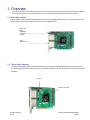
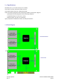
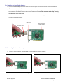
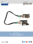
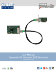
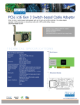
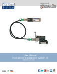
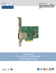
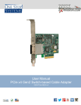
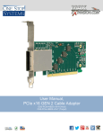
User Manual, PCIe x8 Gen3 Dual and Quad Cable Adapters OSS-PCIe-HIB38-x8-DUAL OSS-PCIe-HIB38-x8-QUAD Table of Contents 1. Overview 1.a. Host cable adapter ................................................................................................................................ 3 1.b. Target cable adapter ............................................................................................................................. 3 1.c. Specifications ........................................................................................................................................ 4 1.d. block diagram ........................................................................................................................................ 4 2. Switch Settings 2.a. Switch Settings ...................................................................................................................................... 5 3. Initial set-up 3.a. Unpacking instructions .......................................................................................................................... 5 3.b. Installation and Removal ....................................................................................................................... 5 3.c. Installing the host cable adapter ............................................................................................................ 6 3.d. Removing the host cable adapter .......................................................................................................... 6 3.e. When using with any third party I/O device ........................................................................................... 7 4. Ordering information 4.a. Ordering Information ............................................................................................................................. 7 5. Appendix 5.a. Appendix... ............................................................................................................................................ 7-12 One Stop Systems Rev. A OSS-PCIe-HIB38-x8-DUAL/QUAD Page 2 1. Overview This manual describes two boards, the base board which provides the dual port adapter and the mezzanine when added to the base board provides the quad port adapter. There are no software drivers required to operate these boards. 1.a. Host cable adapter The host adapters (Part # OSS-PCIe-HIB38x8-DUAL and OSS-PCIe-HIB38X8-QUAD) install in the host computer’s PCIe x16 I/O slot, allowing communication between the processor and multiple I/O points. Slot Cover (Also available in low profile height) PCIe x8Connector 1.b. Target cable adapters The target cable adapters (Part# OSS-PCIe-HIB38-x8-DUAL and OSS-PCIe-HIB38X8-QUAD) install into the target slot of any OSS target backplane and extend the PCIe bus to a single or multiple add-in boards installed in the I/O slots of the target backplane. Switch Mezzanine connector One Stop Systems Rev. A OSS-PCIe-HIB38-x8-DUAL/QUAD Page 3 1.c. Specifications Dimensions (H x L): 4.0 x 5.85 inches (10.16 x 14.85Cm) Front Panel Connectors: Dual PCIe x8 cable connector Front Panel Indicators: Power On / Cable Present LEDs Power Consumption (designed to meet the following conditions) 3.75W typical, [email protected] Operating Environment (designed to meet the following conditions) Temperature Range: 0° to 50°C (32° to 122°F) Relative Humidity: 10 to 90% non-condensing Agency Compliance: UL60950.FCC Class B, CE safety and emissions 1.d. Block Diagram Quad Mezzanine Dual Board One Stop Systems Rev. A OSS-PCIe-HIB38-x8-DUAL/QUAD Page 4 2. Switch Settings 3. Initial Set-Up 3.a. Unpacking Instructions 1) If the carton is damaged when you receive it, request that the carrier’s agent be present when you unpack and inspect the equipment. 2) After unpacking, verify that all items listed in the packing list are present. 3) Inspect the equipment for shipping damage. 4) Save all packing material for storage or return shipment of the equipment. 3.b. Installation and Removal 1) Power down the host system. 2) Open the chassis according to your system documentation. 3) Remove the host cable adapter from the protective bag, observing proper ESD safety procedures. One Stop Systems Rev. A OSS-PCIe-HIB38-x8-DUAL/QUAD Page 5 3.c. Installing the Host Cable Adapter: 1) Insert the host cable adapter into a PCIe Gen3 x16 in the host system slot. Make sure that the card is well seated and tighten the screw on the face plate. 2) Attach the cable by first pulling back on the retractor ring. With the keyed slot aligned with the connector key ridge on the slot cover, insert the cable connector into the connector shell on the board until the connector teeth snap securely into the holes in the cable shell. 3) The connectors on either end of the PCIe x8 cable are identical. Each connector is equipped with a retractor to allow the connector to be locked into place. Holes in the Cable Shell Output swing control dip switch (Table 2) Connector Teeth 3.d. Removing the host cable adapter 1) To remove cable pull back on green thumb tab to release metal pins and gently separate. 2) Loosen and remove the screw before removing the Host Cable Adapter from the card slot. One Stop Systems Rev. A OSS-PCIe-HIB38-x8-DUAL/QUAD Page 6 3.e. When using with any third party I/O device: 1) Install the downstream board into the appropriate PCIe slot. 2) Connect the external power source (separate from the host system power supply) to the downstream device if necessary. 3) Connect the PCIe cable to both the upstream host adapter and the downstream device. 4. Ordering Information OSS-PCIe-HIB38-x8-DUAL – PCIe x8 Gen3 host cable adapter installs in a x4, x8 or x16 expansion slot of a host system to extend the host bus to an expansion system or PCIe device. OSS-PCIe-HIB38-x8-QUAD - PCIe x8 mezzanine board is attached to the dual board adding 2 additional slots Order online at www.maxexpansion.com or call toll free 877-438-2724 Appendix Pin Assignments Connectors PCIe x8 Card Edge Connector The pins are numbered as shown with side A on the top of the centerline on the solder side of the board and side B on the bottom of the centerline on the component side of the board. The PCIe interface pins PETpx, PETnx, PERpx, and PERnx are named with the following convention: “PE” stands for PCIe high speed, “T” for Transmitter, “R” for Receiver, “p” for positive (+), and “n” for negative (-). Note that adjacent differential pairs are separated by two ground pins to manage the connector crosstalk. Customer target mode signals for use with OSS products One Stop Systems Rev. A OSS-PCIe-HIB38-x8-DUAL/QUAD Page 7 Side B Side A Pin # Name Description Name Description 1 +12V 12V Power PRSNT1# Hot-Plug presence detect 2 +12V 12V Power +12V 12V Power 3 +12V 12V Power +12V 12V Power 4 GND Ground GND Ground 5 SMCLK SMBus clock JTAG2 TCK 6 SMDAT SMBus data JTAG3 TSTCLK+ 7 GND Ground JTAG4 TSTCLK- 8 +3.3V 3.3 V power JTAG5 TMS 9 JTAG1 PWR_ON# +3.3V 3.3 V power 10 3.3Vaux 3.3 V auxiliary power +3.3V 3.3 V power 11 WAKE# Signal for link reactivation PERST# Fundamental reset Mechanical key 12 RSVD Reserved GND 13 GND Ground REFCLK+ 14 PETp0 15 PETn0 16 GND Ground PERp0 17 PRSNT2# Hot-Plug presence detect PERn0 18 GND Ground GND Ground 19 PETp1 RSVD Reserved 20 PETn1 GND Ground 21 GND Ground PERp1 22 GND Ground PERn1 23 PETp2 24 PETn2 25 GND Ground PERp2 26 GND Ground PERn2 27 PETp3 28 PETn3 29 GND Ground PERp3 30 RSVD Reserved PERn3 31 PRSNT2# Hot-Plug presence detect GND Ground 32 GND Ground RSVD Reserved 33 PETp4 RSVD Reserved 34 PETn4 GND Ground 35 GND Ground PERp4 36 GND Ground PERn4 37 PETp5 38 PETn5 39 GND Ground PERp5 40 GND Ground PERn5 One Stop Systems Rev. A Transmitter differential pair, Lane 0 Transmitter differential pair, Lane 1 Transmitter differential pair, Lane 2 Transmitter differential pair, Lane 3 Transmitter differential pair, Lane 4 Transmitter differential pair, Lane 5 REFCLK GND Ground Reference clock (differential pair) Ground Receiver differential pair, Lane 0 Receiver differential pair, Lane 1 GND Ground GND Ground Receiver differential pair, Lane 2 GND Ground GND Ground Receiver differential pair, Lane 3 Receiver differential pair, Lane 4 GND Ground GND Ground Receiver differential pair, Lane 5 OSS-PCIe-HIB38-x8-DUAL/QUAD Page 8 41 PETp6 42 PETn6 43 GND Ground PERp6 44 GND Ground PERn6 45 PETp7 46 PETn7 47 GND Ground PERp7 48 PRSNT2# Hot-Plug presence detect PERn7 49 GND Ground GND Transmitter differential pair, Lane 6 Transmitter differential pair, Lane 7 GND Ground GND Ground Receiver differential pair, Lane 6 GND Ground GND Ground Receiver differential pair, Lane 7 Ground Table 1: Pin-out for the PCIe Gen3 x8 Card Edge Connector on the Host Cable Adapter Notes: 1 Optional signals that are not implemented are to be left as no connects on the board side connector. 2 Reserved signals must be left as no connects on the board side connector. 3 Although support of CWAKE# is optional from the board side connector perspective, an allocated wire is mandated for the cable assembly. 4 Board side pin-out on both sides of the Link is identical. The cable assembly incorporates a null modem for the PCIe transmit and receive pairs. PCI Express x8 Connector Pin Assignment Row B, Pin 19 Row A, Pin 1 Row A Row B Row A Row B Pin # Signal Name Signal Name 1 GND 2 3 Row A Row B Pin # Signal Name Signal Name Pin # Signal Name Signal Name GND 13 GND GND 24 PETn4 PERp4 PETp0 PERp0 14 CREFCLK+ PWR (3.3V) 25 GND GND PETn0 PERn0 15 CREFCLK- PWR (3.3V) 26 PETp5 PERp5 4 GND GND 16 GND PWR (3.3V) 27 PETn5 PERn5 5 PETp1 PERp1 17 RSVD PWR RTN 28 GND GND 6 PETn1 PERn1 18 RSVD PWR RTN 29 PETp6 PERp6 7 GND GND 19 SB_RTN PWR RTN 30 PETn6 PERn6 8 PETp2 PERp2 20 CPSRNT$# CWAKE# 31 GND GND 9 PETn2 PERn2 21 CPWRON CPERST# 32 PETp7 PERp7 10 GND GND 22 GND GND 33 PETn7 PERn7 11 PETp3 PERp3 23 PETp4 PETp4 34 GND GND 12 PETn3 PERn3 24 PETn4 PERp4 PIN- out for the PCIe x8 Cable One Stop Systems Rev. A OSS-PCIe-HIB38-x8-DUAL/QUAD Page 9 Signal Descriptions PETp(x) PCI Express Transmit Positive signal of (x) pair. PETn(x) PCI Express Transmit Negative signal of (x) pair. PERp(x) PCI Express Receive Positive signal of (x) pair. PERn(x) PCI Express Receive Negative signal of (x) pair. Cable REFerence CLocK: Provides a reference clock from the host system to the remote system. Side Band ReTurN: return path for single ended signals from remote systems. CREFCLK+/SB_RTN CPRSNT# PWR_RTN Cable PReSeNT: Indicates the presence of a device beyond the cable. PoWeR: Provides local power for in-cable redriver circuits. Only needed on long cables. Power does not go across the cable.) PoWeR ReTurN: Provides local power return path for PWR pins. CWAKE# Cable WAKE CPERST# Cable PCI Express Reset PWR One Stop Systems Rev. A OSS-PCIe-HIB38-x8-DUAL/QUAD Page 10 Mezzanine Connector Pin Out Side B Side A Pin # Pin # Name Description Name Description 1 +12V 12V Power 2 +3.3V +3.3V Power 3 +12V 12V Power 4 +3.3V +3.3V Power 5 N/C Not Connected 6 +3.3Vaux +3.3V auxiliary Voltage 7 N/C Not Connected 8 +3.3V +3.3V auxiliary Voltage 9 PRESENT# Mezzanine Present 10 N/C Not Connected 11 RESET# Reset 12 WAKE# Wake 13 PWrR_GOOD Power Good 14 SMDAT SM Bus Data 15 PWR_ON Power On 16 SMCLK SM Bus Data 17 N/C Not Connected 18 REFCLK- Reference clock (differential pair) 19 N/C Not Connected 20 REFCLK+ Reference clock (differential pair) 21 PERn15 Receiver differential pair, Lane 15 22 PETn0 Receiver differential pair, Lane 0 23 PERp15 Receiver differential pair, Lane 15 24 PETp0 Receiver differential pair, Lane 0 25 PERn14 Receiver differential pair, Lane 14 26 PETn1 Receiver differential pair, Lane 1 27 PERp14 Receiver differential pair, Lane 14 28 PETp1 Receiver differential pair, Lane 1 29 PERn13 Receiver differential pair, Lane 13 30 PETn2 Receiver differential pair, Lane 2 31 PERp13 Receiver differential pair, Lane 13 32 PETp2 Receiver differential pair, Lane 2 33 PERn12 Receiver differential pair, Lane 12 34 PETn3 Receiver differential pair, Lane 3 35 PERp12 Receiver differential pair, Lane 12 36 PETp3 Receiver differential pair, Lane 3 37 PERn11 Receiver differential pair, Lane 11 38 PETn4 Receiver differential pair, Lane 4 39 PERp11 Receiver differential pair, Lane 11 40 PETp4 Receiver differential pair, Lane 4 41 PERn10 Receiver differential pair, Lane 10 42 PETn5 Receiver differential pair, Lane 5 43 PERp10 Receiver differential pair, Lane 10 44 PETp5 Receiver differential pair, Lane 5 45 PERn9 Receiver differential pair, Lane 9 46 PETn6 Receiver differential pair, Lane 6 47 PERp9 Receiver differential pair, Lane 9 48 PETp6 Receiver differential pair, Lane 6 49 PERn8 Receiver differential pair, Lane 8 50 PETn7 Receiver differential pair, Lane 7 51 PERp8 Receiver differential pair, Lane 8 52 PETp7 Receiver differential pair, Lane 7 53 PERn7 Receiver differential pair, Lane 7 54 PETn8 Receiver differential pair, Lane 8 55 PERp7 Receiver differential pair, Lane 7 56 PETp8 Receiver differential pair, Lane 8 57 PERn6 Receiver differential pair, Lane 6 58 PETn9 Receiver differential pair, Lane 9 59 PERp6 Receiver differential pair, Lane 6 60 PETp9 Receiver differential pair, Lane 9 61 PERn5 Receiver differential pair, Lane 5 62 PETn10 Receiver differential pair, Lane 10 63 PERp5 Receiver differential pair, Lane 5 64 PETp10 Receiver differential pair, Lane 10 65 PERn4 Receiver differential pair, Lane 4 66 PETn11 Receiver differential pair, Lane 11 67 PERp4 Receiver differential pair, Lane 4 68 PETp11 Receiver differential pair, Lane 11 69 PERn3 Receiver differential pair, Lane 3 70 PETn12 Receiver differential pair, Lane 12 71 PERp3 Receiver differential pair, Lane 3 72 PETp12 Receiver differential pair, Lane 12 73 PERn2 Receiver differential pair, Lane 2 74 PETn13 Receiver differential pair, Lane 13 75 PERp2 Receiver differential pair, Lane 2 76 PETp13 Receiver differential pair, Lane 13 77 PERn1 Receiver differential pair, Lane 1 78 PETn14 Receiver differential pair, Lane 14 79 PERp1 Receiver differential pair, Lane 1 80 PETp14 Receiver differential pair, Lane 14 81 83 PERn0 PERp0 One Stop Systems Rev. A Receiver differential pair, Lane 0 82 PETn15 Receiver differential pair, Lane 15 Receiver differential pair, Lane 0 84 PETp15 Receiver differential pair, Lane 15 OSS-PCIe-HIB38-x8-DUAL/QUAD Page 12