1
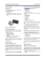
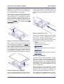
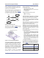
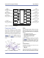
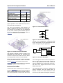
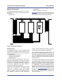
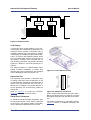
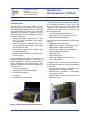
Trenz Electronic GmbH
Brendel 20
32257 Bünde, Germany
www.trenz-electronic.de
Spartan-IIe
Development Platform
2003-January-9
User’s Manual
Introduction
The TE-XC2Se board, the basis of the SpartanIIe Development Platform, comes in the well
known 160x100mm Euro form factor with VG96
connector. The mechanical dimensions and
connectors have been chosen to meet the following requirements:
• convenient for desktop applications
• easy integration into rack-mount systems
• simple and reliable expansion
The Spartan-IIe Development Platform is designed to provide a complete and consistent
FPGA development platform which is especially
well suited to develop FPGA-centric processing
applications. The platform provides all components required to create embedded processor
systems consisting of:
• High-density FPGA, implementing a softCPU, e.g. Xilinx’ MicroBlaze, and application-specific logic
• Memory sub-system combining flash memory and SRAM to store firmware, non-volatile
data and dynamic data
• Peripherals for simple user interaction and
in-system debugging
• Expansion ports to interface with applicationspecific circuitry
In typical desktop applications, the Spartan-IIe
Development Platform does not require any additional hardware or software components besides a standard PC with USB connector. This
makes the Spartan-IIe Development Platform an
ideal solution for:
• Training and education
• Development of intellectual property
• Firmware development
• Prototyping
• Industrial control applications
The TE-XC2Se board provides the following key
features:
• 300K-gate Spartan-IIE FPGA
• 8Mbit (1M x 8 / 512K x 16) of flash memory
• 4Mbit (256K x 16-Bit) of Static RAM
• LCD with 2x16 characters and backlight
• Universal Serial Bus interface
• RS232 interface
• VGA monitor output
• LEDs, DIP switches and push buttons
• Up to 100 user I/Os
In addition to the TE-XC2Se board, the SpartanIIe Development Platform contains the following
components:
• complete FPGA design environment including design entry and HDL synthesis
• Ready-to-Use IP-Modules encapsulating
standard functionality
• Documentation, tutorials and comprehensive
application notes
Figure 1: Spartan-IIe Development Platform
Trenz Electronic GmbH
1
Spartan-IIe Development Platform
User's Guide
Packing List
Your Spartan-IIe Development Platform ships
with the following items:
• TE-XC2Se board
• USB cable
• CD-ROM with FPGA design software, software utilities, documentation, and application
notes
User’s Manual
to a more recent version, visit the Xilinx web site
at www.xilinx.com and download the WebPACK
software with the following options:
• Design Entry
• Spartan Fitter
• Virtex Fitter
• FPGA Programming
Optionally, you may also download the following
modules:
• MXE Simulator
• Verilog FPGA
• VHDL FPGA
• StateCAD
• HDL Bencher
• XPower
• FPGA Schematic Libraries
The complete software package is also available as a single file download with the following
size:
• WebPACK 4.2 FPGA installer: 106MByte
• MXE Simulator installer: 39MByte
Figure 2: Package Contents
System Requirements
The Development Platform and its accompanying software tools have the following minimum
system requirements:
• IBM PC or compatible
• 128MBytes of RAM
• 500MBytes of disk space
• USB port
• Windows 98SE, or Windows Millennium
Windows 2000, or Windows XP
Please note, that the due to the missing USB
support, the TE-XC2Se board is not compatible
with Windows NT.
Software Setup
Install the Design Software
The TE-XC2Se board may be programmed using Xilinx’ free WebPACK ISE package. We recommend using version 4.2 or later. The WebPACK ISE package is an integrated FPGA
development software including design entry,
Verilog and VHDL synthesis, and behavioral
simulation.
In case you did not receive the software with
your TE-XC2Se board, or you need to upgrade
Trenz Electronic GmbH
When installing the software, make sure the install path does not contain blanks. It is recommended to keep the default path suggested by
the installer.
Install the Development Platform Tools
In addition to the design software, the companion CD-ROM contains the following tools:
• download utility to program your designs into
the FPGA
• example designs
• documentation
Copy the contents of the CD-ROM to a directory
of your choice. You should make sure, that the
directory path does not contain blanks.
For convenience, you should create a shortcut
to the TEprog.exe download utility on your desktop.
Hardware Setup
USB-powered Desktop System
The TE-XC2Se board may be powered from the
USB, yielding an extremely convenient desktop
development system, as no additional circuitry,
power-supply or cabling is required. Perform the
following steps to use this setup:
• switch S1 to USB before connecting any
cables
2
Spartan-IIe Development Platform
•
User’s Manual
connect the TE-XC2Se board with the USB
port of your host-PC
In this setup, the switch S1 may also be used as
a power switch, avoiding the need to disconnect
the TE-XC2Se board from the USB. Refer to
Figure 3 to locate the switch S1.
+5V
GND
Figure 4: Externally Powered
Desktop System
Figure 3: USB-powered Desktop System
USB ports are specified to deliver a maximum
current of 500mA. Therefore, you should either
connect your TE-XC2Se board directly to the
host PC, or use a self-powered USB hub (with
its own power-supply).
In rare occasions, you may receive a warning
message from your host PC, stating that the
maximum USB power consumption is exceeded. In these cases, the power LED of the TEXC2Se does not light up. If you encounter problems powering your board from the USB, consider using the externally-powered desktop setup.
Externally-powered Desktop System
In case your system consumes more power,
than the USB ports deliver, you may source your
TE-XC2Se board from an external regulated 5V
power supply. We recommend using an industry-standard computer supply. Perform the following steps to do so:
•
switch S1 to EXT POWER before connecting
any other cables
•
Connect the TE-XC2Se board with the USB
port of your host-PC
•
connect the TE-XC2Se board with your
power supply
See Figure 4 to locate the switch S1.
Trenz Electronic GmbH
Using an external power-supply is recommended in the following scenarios:
• you are working with a laptop and do not
want to draw too much power from it
• you are creating a complex and high-speed
design
• you are planning to attach complex peripherals to the board
• you are working with a bus-powered USB
hub, which only provides 100mA of current
per port
Caution: Using a power supply with the wrong
voltage or polarity may cause permanent damage to the hardware. Double check your setup!
Rack-mount System
The TE-XC2Se board perfectly integrates with
industry-standard 19” rack-mount systems featuring VG96 backplane connectors. To do so,
perform the following steps:
• download your design to the user configuration space, using the USB-powered desktop
setup
• switch S1 to EXT POWER
• mount the TE-XC2Se board into the rack
Caution: Using a power supply with the wrong
voltage or polarity may cause permanent damage to the hardware. Double check, that power
is applied to the correct pins of the VG96 connector!
Expanding the System
The TE-XC2Se board is designed as an expandable system. While the TE-XC2Se board
already provides a set of commonly used pe-
3
Spartan-IIe Development Platform
ripherals, your application may require other,
specialized circuitry, which may be attached to
the TE-XC2Se board in various ways.
The expansion bus is an 8-bit bus, which is suitable to attach standard microprocessor peripherals, like timers, or I/O controllers. The size of
the circuit boards is relatively small, but the expansion unit may provide I/O connectors to the
front panel. Figure 5 details this. Refer to the Expansion Bus section for a complete description
of the available signals.
User’s Manual
to the VG96 connector. All circuitry is easily accessible when doing so, and the boards may be
assembled or de-assembled in a matter of seconds.
Figure 7: Expanding “in line”
Finally, the TE-XC2Se, together with the expansion circuitry, may be installed in an industrystandard 19” rack with a VG96 backplane.
Figure 5: Connecting to the Expansion Port
More complex circuitry may be attached to the
TE-XC2Se board as piggyback, as Figure 6 details. The advantage of doing so is, that all signals routed to the VG96 connector are accessible, the PCB may be up to full Euro format, and
the resulting system is very compact. However,
when attaching a piggyback board, access to
the push buttons and the LCD display is difficult.
Among others, suitable rack-mount systems are
provided from the following manufacturers:
• Schroff
Propac line of cases or
Europack Pro line of subracks
www.schroff.de
• Apw
Diplomat line of 19” cases and case frames
www.apw.com
• Bopla
Combicard II line of card enclosure systems
www.bopla.de
FPGA Programming
The FPGA on the TE-XC2Se board is configured from on-board non-volatile flash memory.
The flash memory in turn is programmed via
Universal Serial Bus. The concept involves two
configurations, both of them being stored in the
flash memory: The user configuration, and the
factory configuration.
Figure 6: Expanding as Piggyback
After power-up, the user configuration is automatically loaded into the FPGA. The user configuration holds the latest user-defined bitstream, which was downloaded to the board.
In case a compact design is not too crucial, it is
highly recommended to attach circuitry “in line”
After pressing the PROGRAM button, the factory configuration is loaded into the FPGA. The
Trenz Electronic GmbH
4
Spartan-IIe Development Platform
factory configuration implements a USB circuitry, which is used to re-program the Flash memory with a new user configuration.
Once the Flash memory is re-programmed, the
user may press RUN to load the updated user
configuration into the FPGA. Refer to Figure 8
for a simple flowchart of this procedure.
power-on
reset
load user
configuration
user
functionality
light D6
press
RUN
press
PROGRAM
USB
download
load factory
configuration
light D7
Figure 8: Programming Flow
The status of the board is indicated by two
LEDs, D6 and D7. Refer to Figure 9 to locate
the programming buttons and the LEDs.
User’s Manual
stream to the board. The following steps need to
be performed to do so:
• connect the board to the USB
• load the factory configuration by pressing the
PROGRAM button
• run TEprog.exe
TEprog.exe uses the following syntax:
TEprog bitfile
TEprog /a rawfile
TEprog /f bitfile
When used without a parameter, the bitstream
contained in bitfile is loaded to the user configuration space of the flash memory (0x40000).
When used with the /a parameter, the rawfile is
loades to the application space of the flash
memory (0x80000).
When used with the /f parameter, the bitstream
contained in bitfile is loaded to the factory configuration space of the flash memory.
Caution: Do not re-program the factory configuration space, unless you know exactly what you
are doing! Once you re-programmed the factory
configuration, downloading bitstreams via USB
may no longer work!
For your daily work, we recommend using one
of the following setups:
• Add a shortcut to TEprog.exe to your desktop. You may program a bitstream to the user
configuration space, by just dragging a bitfile
onto this shortcut.
• Create a batch file calling TEprog.exe with
the appropriate parameters. Add this batch
file to your WebPACK ISE project. A simple
double click on this file will program the bitstream to the board- without leaving the Xilinx Project Navigator.
Figure 9: Locate Programming Buttons
The bitstreams loaded into the flash memory do
not need be formatted by the Xilinx PROM File
Formatter. Instead, the bitstreams are downloaded to the board exactly as being created by
Xilinx bitgen. The FPGA is configured in Slave
Parallel Mode. To do so, the Start-Up Clock
must be set to CCLK. Refer to the WebPACK
ISE documentation for further details.
Once a bitstream is created, the TE-XC2Se
download utility is used to download the bit-
Trenz Electronic GmbH
The duration of the download to the Flash memory depends on the type of the USB host controller- and not on the speed of your host PC.
Refer to Table 1 for typical download durations.
USB host controller
duration
[seconds]
UHCI (Intel or VIA chipsets)
38
OHCI (OPTi chipsets)
14
EHCI (USB 2.0 chipsets)
12
Table 1: Download Durations
5
store
config & firmware
store
processing data
simple
user input
Universal
Serial Bus
FPGA
300,000 gates
Flash memory
512K x 16-Bit
static RAM
256K x 16-Bit
memory bus
download
designs
User’s Manual
expansion bus
Spartan-IIe Development Platform
LCD
2 x 16 characters
expansion
port
RS232
serial port
CPLD
VGA monitor
output
switches, buttons,
LEDs
VG96
connector
display
attach
add-ons
debug
firmware
visualize
expand the
system
clocks, reset, power supply
Figure 10: TE-XC2Se Block Diagram
Programmer's Models
This section describes the various building
blocks of your TE-XC2Se board, and how they
interact with the FPGA, from a programmer's
perspective. To better serve this purpose, simplified schematics and block diagrams are used.
Figure 10 shows a block diagram of the TEXC2Se board. Figure 11 helps to locate the
most important components on the TE-XC2Se
board.
FPGA
The XC2S300E-6FT256C FPGA from Xilinx'
Spartan-IIE family of devices is the main repository of programmable logic on your TE-XC2Se
board. The device provides the following key
features:
• Up to 300,000 system gates
• Up to 200MHz of system performance
• Up to 98kBits of distributed RAM
• 64kBits of dedicated block RAM
• 182 User I/Os
To help measuring the capacity of the FPGA,
the Table 2 summarizes the resource usage of
some common building blocks. Please note,
that these are only rough approximations, which
are highly dependent upon the actual application.
Clocks & Reset
To provide clock signals to the FPGA, two clock
oscillators are provided:
• USB clock
• User clock
Figure 11: Locate Basic Components
Trenz Electronic GmbH
The USB clock provides a clock frequency of
48MHz, as required to implement the USB interface. This clock cannot be altered, to ensure
6
Spartan-IIe Development Platform
User’s Manual
Function
Resource Usage
Xilinx MicroBlaze
32-bit RISC CPU
950 LUTs
15%
USB Function Controller
380 LUTs
6%
8051 microcontroller
including peripherals
2500 LUTs
40%
8-bit RISC CPU
250 LUTs
4%
Table 2: XC2S300E Resource Usage
proper operation of the USB download mechanism under all circumstances.
The user clock provides a clock frequency of
25MHz, suitable as dot clock for the VGA output. However, the oscillator may be substituted
by any other canned crystal oscillator, depending on your application's requirements. Refer to
Figure 12 to locate the clock oscillator.
Figure 13: Locate Reset Button
P15 (INIT#)
S9/RESET
T9 (GCK0)
USB clock
B8 (GCK2)
user clock
FPGA
Figure 14: Clock & Reset Circuitry
running a user configuration, customized USB
device functionality may be implemented in the
FPGA, if required by your application.
D+
D-
Figure 12: Locate User Clock Oscillator
The Spartan-IIe FPGA provides a total of four
dedicated clock input pins, the remaining two
clocks are routed to the VG96 connector. Refer
to the appropriate section for further details.
Button S9, labelled RESET, is used to provide
an asynchronous active-low reset to the FPGA.
Refer to Figure 13 to locate the reset button.
Figure 14 illustrates the circuitry as simplified
schematic diagram for quick reference.
Universal Serial Bus
A USB transceiver is attached to the FPGA, as
shown in Figure 15. With the FPGA running the
board's factory configuration, the flash memory
may be programmed via USB. With the FPGA
Trenz Electronic GmbH
USB
transceiver
USB
J22
CON
A8
VP
VM
RCV
D9
C9
B9
VPO
FSE0
OE#
E11
D12
E10
FPGA
Figure 15: Universal Serial Bus
The CON signal is used to switch the pull-up resistor in the D+ line. By driving the CON pin to
Vcc or high-impedance, the USB connection
may be established or closed under FPGA control. This in turn, triggers the host PC to re-run
USB enumeration.
The USB transceiver is wired for 12Mbps (full
speed) operation, with the output driver in
Mode 0. Consult the USB transceiver’s data
sheet for pin descriptions and signal waveforms.
7
Spartan-IIe Development Platform
User’s Manual
Memory Subsystem
•
•
The memory subsystem consist of a 16-bit bus,
the memory bus, with the following devices attached to it:
• flash memory
Static RAM
Buttons, switches, and LEDs
Figure 16 illustrates the memory subsystem. As
all devices share the same set of bus signals,
the access to the bus is mutually exclusive.
A[21:1]
D[7:0]
A[2:1]
D[15:0]
CPLD
D15
D14
D13
D12
D11
D10
D9
D8
D7
D6
D5
D4
D3
D2
D1
D0
J13
J16
J15
K13
K12
L12
K16
K15
P16
L16
L13
J14
G15
F14
E15
B16
CS#
R/ W#
static RAM
256K x 16-bit
CS#
OE#
BLE#
BHE#
WE#
A[18:1]
D[15:0]
flash memory
512K x 16-bit
CE#
OE#
BYTE#
RY/ By#
WE#
A21
A20
A19
A18
A17
A16
A15
A14
A13
A12
A11
A10
A9
A8
A7
A6
A5
A4
A3
A2
A1
A[19:1]
D[15:0]
P9
N9
R14
T14
P10
R10
T11
R11
P12
T12
R12
P11
T13
R13
M11
P13
N12
N11
N10
M10
T10
N16
N14
M14
N15
M13
L14
L15
K14
M16
M15
R9
FPGA
FPGA
Figure 16: Memory Subsystem
Flash memory
An AMD flash memory of type AM29LV800B
with 8Mbits of storage (1Mx8/ 512Kx16) is attached to the memory bus, to store the following
non-volatile data:
• FPGA factory configuration
• FPGA user configuration
• application data
The FPGA factory configuration is used, to program the flash memory via USB. The factory
configuration is loaded into the FPGA, whenever button S7, labelled PROGRAM, is pressed.
The factory configuration occupies 256kB of
memory and should not be altered.
The FPGA user configuration stores your FPGA
design and is loaded into the FPGA, during
power-up, or whenever button S8, labelled
RUN, is pressed. The user configuration occupies 256kB of memory, and the associated
Trenz Electronic GmbH
memory space should not be used for other purposes than storing an FPGA configuration.
The application data space may be used to
store various application-dependent data, e.g.
firmware or data received from a measurement
unit. The application space provides 512kB of
memory and may be read and written under application control.
It is highly recommended, using the download
utility supplied with the Spartan-IIe Development
Platform to program the flash memory. Special
care should be taken, not to overwrite the factory configuration, as this will inhibit future programming of the flash memory via USB. Further
details on the download mechanism may be
found in the FPGA Programming section of this
document. Consult the flash memory’s data
sheet for timing diagrams and a description of
the command set.
8
Spartan-IIe Development Platform
User’s Manual
Usage
Location
Function
Location
Direction
factory configuration
0x00000-0x3FFFF
0x40000-0x7FFFF
application space
0x80000-0xFFFFF
0x00001
Bit 0
Bit 1
Bit 2
Bit 3
Bit 4
Bit 5
Bit 6
Bit 7
read-only
user configuration
DIP switch
S2-1
S2-2
S2-3
S2-4
S2-5
S2-6
S2-7
S2-8
push buttons
PB1
PB2
PB3
PB4
0x00000
Bit 0
Bit 1
Bit 2
Bit 3
read-only
LEDs
L1
L2
L3
L4
0x00002
Bit 0
Bit 1
Bit 2
Bit 3
write-only
LED
L5
FPGA
Pin C15
-
Table 3: Flash Memory Map
SRAM
An IDT asynchronous Static RAM of type
IDT71V416S is attached to the memory bus, to
store volatile data, e.g. a processor system's
stack and heap data.
The RAM is fast enough to serve as zero-waitstate main memory for typical processing applications. Consult the RAM’s data sheet for timing
diagrams.
Switches, Buttons, and LEDs
The board provides a set of eight DIP switches,
four push buttons, and four LEDs. Refer to
Figure 17 to locate the components.
Table 4: CPLD Memory Map
The CPLD read and write waveforms are similar
to those of asynchronous RAMs. Refer to
Figure 18 and Figure 19 for details.
A[2:1]
CS#
R/W#
Figure 18: CPLD Read Waveforms
A[2:1]
CS#
R/W#
Figure 17: Locate Switches, Buttons, LEDs
The switches, buttons and LEDs are attached to
the CPLD, which is in turn attached to the memory bus. Table 4 shows the peripheral's memory
map.
Note, that the registers are uni-directional, i.e.
the LED register may not be read and the switch
or button registers may not be written.
Trenz Electronic GmbH
Figure 19: CPLD Write Waveforms
Expansion Bus
The TE-XC2Se board offers an 8-bit expansion
bus, which can be used to expand the board
with small form factor peripherals. The expansion bus is shared with the liquid crystal display,
access to LCD or expansion bus is mutually exclusive. Refer to Figure 20 for a simplified schematic.
9
Spartan-IIe Development Platform
User’s Manual
A[2:0]
G13
G14
G16 (L30P)
H16 (L30N)
E16 (L26P)
F15 (L26N)
A9 (L9N)
H14
D16
D[7:0]
A[2:0]
RW
E
E#
LCD
2 x 16 characters
D7
D6
D5
D4
D3
D2
D1
D0
expansion
port
GPIO-1P
GPIO-1N
GPIO-2P
GPIO-2N
GPIO-3
CS#
RW
A0
D[7:0]
D[7:0]
H15 A2
F16 A1
H13 A0
FPGA
G12
F13
F12
E14
E13
D15
D14
C16
FPGA
Figure 20: Expansion Bus
LCD Display
A Polytronix liquid crystal display of type PC160203 with 2x16 characters is attached to the
expansion bus to provide a convenient way of
visualizing textural data. The display is capable
of displaying the complete range of ASCII characters, as well as user-defined symbols. Refer
to the according data sheet for a description of
the display’s character and command set, as
well as timing information. Signal E# is direction
signal for a busdriver, and must be always negated E.
The display features an LED backlight, which
greatly increases readability. In setups with
stringent low-power requirements, the backlight
may be disabled by removing jumper J19.
Expansion Port
The expansion port provides a convenient way
of adding small form factor expansions to the
TE-XC2Se board. Virtually any peripheral with a
generic 8-bit microcontroller bus may be attached here. In addition, five general purpose I/
Os are provided, four of them being usable as
LVDS pairs.
Refer to Figure 21 to locate the connector,
Figure 22 details the connector pinout.
Serial Port Connector
To interface standard RS232 peripherals with
the TE-XC2Se board, a level shifter is attached
to the FPGA. The required UART functionality
may be efficiently implemented in the FPGA.
Trenz Electronic GmbH
Figure 21: Locate Expansion Port
+5V
GPIO1-P
GPIO2-P
GPIO3
D1
D3
D5
D7
CS#
A1
48MHz
reserved
reserved
1
3
5
7
9
11
13
15
17
19
21
23
25
2
4
6
8
10
12
14
16
18
20
22
24
26
+3.3V
GPIO1-N
GPIO2-N
D0
D2
D4
D6
RW
A0
A2
RESET#
reserved
GND
Figure 22: Expansion Port Pinout
When working with soft-CPUs like Xilinx' MicroBlaze, the serial port may be used for in-system
debugging using gdb from the GNU tools collection.
The RS232 implements no handshake signals.
Figure 23 shows a simplified schematic dia-
10
Spartan-IIe Development Platform
User’s Manual
1
2
3
4
5
RED
GREEN
BLUE
N.C.
GND
gram, refer to Figure 24 for the connector pinout.
TxD
RxD
B13
C12
RS232
J20
N.C.
N.C.
/HSYNC
/VSYNC
N.C.
11
12
13
14
15
TxD
RxD
FPGA
Figure 26: VGA Connector Pinout
Figure 23: RS232 Circuitry
1
2
3
4
5
DCD
RxD
TxD
DTR
GND
JTAG
DSR
RTS
CTS
N.C.
6
7
8
9
To allow full flexibility in programming/ configuring the FPGA and CPLD, the JTAG chain is accessible on a separate jumper. Figure 27 illustrates the JTAG chain.
Figure 24: RS232 Connector Pinout
TMS
TCK
VGA Monitor Interface
TDI
The TE-XC2Se board provides circuitry to interface with industry-standard VGA monitors. To
do so, RGB tuples along with horizontal and vertical sync pulses need to be generated inside
the FPGA. A simple passive DAC creates the
required analog signals. Refer to Figure 25 for a
simplified schematic.
C10
D10
B11
A11
D11
C11
B10
A10
R0
R1
G0
G1
B0
B1
R
CPLD
TDO
TDI
FPGA
TDI
TDO
JTAG
J23
Figure 27: JTAG Chain
The pinout of J23 is compatible to the flying
leads of Xilinx’ Parallel Cable III. Refer to
Figure 28 for the connector pinout.
G
B
1
2
3
4
5
6
7
8
9
/HSYNC
/VSYNC
FPGA
VGA
J21
Figure 25: VGA Output Circuitry
Due to the simple design, the maximum dot
clock of the VGA output is limited. As a rule of
thumb a dot clock of 25MHz for 640x480 resolution at 60Hz vertical frequency is a good value.
Figure 26 details the pinout of the VGA connector.
+3.3V
GND
N.C.
TCK
N.C.
TDO
TDI
N.C.
TMS
Figure 28: JTAG Connector Pinout
Before using JTAG to configure the FPGA, the
configuration mode should be set accordingly.
This is accomplished with J18, refer to Table 5
for the proper settings.
Function
J18 setting
slave parallel mode
open
boundary scan mode
closed
Table 5: J18 Settings
Trenz Electronic GmbH
11
Spartan-IIe Development Platform
User’s Manual
Please note, that access to the flash memory
via JTAG is not supported. However, this may
be accomplished by using additional software.
It is highly recommended not to re-program the
CPLD unless you know exactly what you are doing. Reprogramming the CPLD may break the
mechanism which is configuring the FPGA from
flash memory.
Refer to Figure 29 to locate the JTAG components.
Figure 30: Locate Vcco Jumpers
The complete I/O banks 5, 6, 7, and 0 of the
FPGA are routed to the VG96 connector,
Table 6 lists the available signals. The piggyback connectors J2, J3, and J4 are wired in parallel with rows A, B, and C of the VG96 connector. Refer to Figure 31 to locate the piggyback
connector.
Figure 29: Locate JTAG Connector
VG96 Connector
A VG96 connector is used, to attach customized
peripherals to the board. The connector is designed to provide full access to the FPGA's various I/O standards, including its LVDS pairs, and
access to the Vcco and Vref pins.
The Vref voltages are applied to a number of
dual-purpose pins on the VG96 connector. See
the Spartan-IIE data sheet for further details.
The Vcco voltages are set to either 1.8V, 2.5V,
or 3.3V using 4 banks of jumpers. Refer to
Trenz Electronic GmbH
Figure 31: Locate Piggyback Connector
12
Spartan-IIe Development Platform
Pin
User’s Manual
A / J2
B / J3
C / J4
Pin
Function
Bank
Pin
Function
Bank
Pin
Function
Bank
1
-
+5V ext
-
-
+5V ext
-
-
+5V ext
-
2
R8
I/O (DLL)
5
M6
L55N
5
T8
GCK1
5
3
R7
L54N
5
P8
I/O
5
T7
L54P
5
4
R6
L56N (Vref)
5
P7
I/O
5
T6
L56P
5
5
R5
L58N (Vref)
5
T4
L60P
5
T5
L58P
5
6
M7
L53N (Vref)
5
N7
L55P
5
N8
L53P
5
7
N6
L57N
5
R4
L61P
5
P6
L57P
5
8
N5
L59N
5
T3
L60N (Vref)
5
P5
L59P
5
9
K5
L68N
6
P4
L61N
5
K4
L68P
6
10
P2
L62N
6
M4
L64N
6
P1
L62P
6
11
N1
L66N
6
M3
L64P
6
M1
L66P
6
12
N3
L63N (Vref)
6
M2
L67N (Vref)
6
N2
L63P
6
13
L2
L69N
6
L3
L67P
6
L1
L69P
6
14
K3
L70N
6
K1
L71N (Vref)
6
K2
L70P
6
15
L5
L65N (Vref)
6
J1
L71P
6
L4
L65P
6
16
J3
L72N
6
J4
I/O
6
J2
L72P
6
17
H1
L73N
7
G1
L75N
7
H2
L73P
7
18
H3
L74N
7
G2
L75P (Vref)
7
H4
L74P
7
19
G4
L76N
7
F1
L78N
7
G3
L76P
7
20
F3
L79N
7
F2
L78P
7
F4
L79P (Vref)
7
21
E1
L80N
7
E3
L81P (Vref)
7
E2
L80P
7
22
D1
L82N
7
E4
L81N
7
D2
L82P
7
23
C1
L83N (Vref)
7
D3
I/O
7
C2
L83P
7
24
G5
L77N
7
B3
I/O
0
F5
L77P
7
25
E6
L3N
0
B4
L1P
0
D6
L3P
0
26
A3
L0N (Vref)
0
C4
L1N
0
A4
L0P
0
27
B5
L4N (Vref)
0
A6
I/O
0
A5
L4P
0
28
C5
L2N (Vref)
0
A7
I/O
0
D5
L2P
0
29
C6
L5N
0
C7
L6P
0
B6
L5P
0
30
-
+3.3V out
-
B7
L6N
0
E7
L7P
0
31
D8
I/O (DLL)
0
D7
L7N (Vref)
0
C8
GCK3
0
32
-
GND
-
-
GND
-
-
GND
-
Table 6: VG96 Connector Pinout
Trenz Electronic GmbH
13
Spartan-IIe Development Platform
Appendix
References
•
•
•
•
•
Spartan-IIE 1.8V FPGA Family
Xilinx, November 9, 2001
FastFLASH XC9500XL
High-Performance CPLD Family
Xilinx, June 7, 1999
Am29LV800B
8 Megabit (1M x 8-Bit/ 512 K x 16-Bit)
CMOS 3.0 Volt-only
Boot Sector Flash Memory
AMD, August 14, 2000
IDT71V416S
IDT71V461L
3.3V CMOS Static RAM
4 Meg (256K x 16-Bit)
IDT, August 2000
Character Type LCD Module
PC-160203
Product Specification
Polytronix Inc, June, 2001
Trenz Electronic GmbH
User’s Manual
•
•
•
•
HD44780U (LCD-II)
(Dot Matrix Liquid Crystal Display Controller)
Hitachi, September, 1999
PDIUSBP11A
Universal Serial Bus Transceiver
Data Sheet
Philips Semiconductors, June 4, 1999
ISE 4 User Guide
Xilinx, July 2001
Development System Reference Guide
ISE 4
Xilinx, July 2001
Revision History
Version
Date
Who
Description
0.99
2002apr04
FB
Created
1.00
2002jul18
TT
Revised
1.01
2002aug16
TT
Minor changes
Table 7: Revisions History
14