1
WIZ820io User Manual
(Version 1.0)
© 2011 WIZnet Co., Ltd. All Rights Reserved.
☞ For more information, visit our website at http://www.wiznet.co.kr
WIZ820io User Manual (WIZnet Co., Ltd.)
1
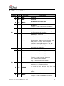
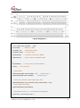
Document Revision History
Date
Revision
2011-09-15
V1.0
Changes
Official Release
WIZ820io User Manual (WIZnet Co., Ltd.)
2
1. Introduction
WIZ820io is the internet offload network module that includes W5200 (TCP/IP
hardwired chip, include PHY), MAG-JACK (RJ45 with X’FMR) with other glue logics.
It can be used as a component and no effort is required to interface W5200 and
Transformer.
The WIZ820io is an ideal option for users who want to develop their Internet
enabling systems rapidly.
For the detailed information on implementation of Hardware TCP/IP, refer
to the W5200 Datasheet.
WIZ820io consists of W5200 and MAG-JACK.
TCP/IP, Ethernet MAC : W5200
Ethernet PHY : Included in W5200
Connector : MAG-JACK(RJ45 with Transformer)
1.1 Feature
Supports 10/100 Base TX
Supports half/full duplex operation
Supports auto-negotiation and auto cross-over detection
IEEE 802.3/802.3u Compliance
Supports high speed SPI Interface (SPI mode 0, 3)
Operates 3.3V with 5V I/O signal tolerance
Supports network status indicator LEDs
Includes Hardware Internet protocols: TCP, IPv4, UDP, ICMP, ARP, PPPoE,
IGMP
Includes Hardware Ethernet protocols: DLC, MAC
Supports 8 independent connections simultaneously
Supports Power down mode
Supports Wake On LAN
Supports Socket API for easy application programming
Interfaces with two 2.54mm pitch 1 x 6 header pin
Very small form factor: 23mm x 25mm (PCB size)
WIZ820io User Manual (WIZnet Co., Ltd.)
3
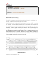
2. Pin assignment & description
2.1 Pin assignment
< TOP side view >
< Pin assignment >
WIZ820io User Manual (WIZnet Co., Ltd.)
4
2.2 Pin description
Pin No.
I/O
Pin Name
Description
1
P
GND
Ground
2
P
GND
Ground
3
I
MOSI
4
I
SCLK
SPI Master Out Slave In
This pin is used to SPI MOSI signal pin.
SPI Clock
This pin is used to SPI Clock Signal pin.
SPI Slave Select : Active Low
5
I
nSS
J1
This pin is used to SPI Slave Select signal
Pin when using SPI interface.
Interrupt : Active low
This pin indicates that W5200 requires MCU
attention after socket connecting,
6
O
nINT
disconnecting, data receiving timeout, and
WOL (Wake on LAN). The interrupt is
cleared by writing IR Register or Sn_IR
(Socket n-th Interrupt Register). All
interrupts are maskable.
1
P
GND
Ground
2
P
3V3D
Power : 3.3 V power supply
3
P
3V3D
Power : 3.3 V power supply
Power Down : Active High
4
I
PWDN
This pin is used to power down pin.
Low : Normal Mode Enable
High : Power Down Mode Enable
J2
Reset : This pin is active low input to
initialize or re-initialize W5200.
5
I
nRESET
It should be held at least 2us after low
assert, and wait for at least 150ms after
high de-assert in order for PLL logic to be
stable.
6
O
MISO
WIZ820io User Manual (WIZnet Co., Ltd.)
SPI Master In Slave Out
This pin is used to SPI MISO signal pin.
5
3. Device SPI operations
WIZ820io is controlled by a set of instruction that is sent from a external host ,
commonly referred to as the SPI Master. The SPI Master communicates with
W5200 via the SPI bus, which is composed of four signal lines: Slave Chip Select
(nSS), Serial Clock (SCLK), MOSI (Master Out Slave In) and MISO (Master In
Slave Out).
The SPI protocol defines four modes for its operation (Mode 0-3). Each mode
differs according to the SCLK polarity and phase - how the polarity and phase
control the flow of data on the SPI bus. The W5200 operates as SPI Slave device
and supports the most common modes - SPI Mode 0 and 3.
The only difference between SPI Mode 0 and 3 is the polarity of the SCLK signal
at the inactive state. With SPI Mode 0 and 3, data is always latched in on the
rising edge of SCLK and always output on the falling edge of SCLK.
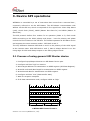
3.1 Process of using general SPI Master device
1. Configure Input/Output direction on SPI Master Device pins.
2. Configure nSCS as ‘High’ on inactive
3. Write target address for transmission on SPDR register (SPI Data Register).
4. Write OP code and data length for transmission on SPDR register.
5. Write desired data for transmission on SPDR register.
6. Configure nSCS as ‘Low’ (data transfer start)
7. Wait for reception complete
8. If all data transmission ends, configure nSCS as ‘High’
0
1
2
Address
OP Code (1bit) + data length n (16bit)
data1
n data
...
data n-1
Bit
0 1
2 3 4
5
Byte
6
7
Byte
< W5200 SPI Frame Format >
WIZ820io User Manual (WIZnet Co., Ltd.)
6
< Address and OP/DATA Length Sequence Diagram >
3.2 Read processing
The READ processing is entered by driving nSS low, followed by the Address, the
OP code, the Data Length and the Data byte on MOSI. The OP code (OP) is
defined type of the READ OP and WIRTE OP. On OP = 0, the read operation is
selected. Otherwise, On OP = 1, the write operation is selected.
In W5200 SPI mode, the Byte READ processing and the burst READ processing
are provided. The Byte READ processing takes 4 instructions which is consist of
the 16-bit Address, the 1-bit OP code(0x0), the 15-bit Data length and 8-bit Data.
Otherwise, The Burst READ processing only takes the Data instruction after the
setting of the burst read processing. To distinguish between the Byte READ and
the burst READ processing, the Data length is used. If the Data length is ‘1,’ the
Byte READ processing is operated. Otherwise, the Burst READ Processing is
operated when the Data length is more than two. The MISO pin should be
selected by driving MISO low after the falling edge of the nSS.
WIZ820io User Manual (WIZnet Co., Ltd.)
7
< Read Sequence >
/* Pseudo Code for Read data of 8bit per packet */
#define data_read_command
uint16 addr;
0x00
// Address : 16bits
int16 data_len;
// Data length :15bits
uint8 data_buf[];
// Array for data
SpiSendData();
// Send data from MCU to W5200
SpiRecvData();
// Receive data from W5200 to MCU
{
ISR_DISABLE();
CSoff();
// Interrupt Service Routine disable
// CS=0, SPI start
// SpiSendData
SpiSendData(((addr+idx) & 0xFF00) >> 8);
SpiSendData((addr+idx) & 0x00FF);
// Address byte 1
// Address byte 2
// Data write command + Data length upper 7bits
SpiSendData((data_read_command| ((data_len& 0x7F00) >> 8)));
// Data length bottom 8bits
SpiSendData((data_len& 0x00FF));
// Read data:On data_len> 1, Burst Read Processing Mode.
for(int idx = 0; idx<data_len; idx++)
{
WIZ820io User Manual (WIZnet Co., Ltd.)
8
SpiSendData(0);
// Dummy data
data_buf[idx] = SpiRecvData(idx);
// Read data
}
CSon();
// CS=1, SPI end
ISR_ENABLE();
// Interrupt Service Routine disable
}
3.3 Write processing
The WRITE processing is entered by driving nSS low, followed by the Address, the
OP code, the Data Length, and the Data byte on MISO.
In W5200 SPI mode, the Byte WRITE processing and the Burst WRITE processing
are provided. The Byte WRITE processing takes 4 instructions which is consist of
the 16-bit Address, the 1-bit OP code(0x1), the 15-bit Data length and 8-bit Data.
Otherwise, The Burst WRITE processing only takes the Data instruction after the
setting of the Burst WRITE processing. To distinguish between the Byte WRITE and
the Burst WRITE processing, the Data length is used. If the Data length is ‘1,’ the
Byte WRITE processing is operated. Otherwise, the Burst WRITE Processing is
operated when the Data length is more than two. The MOSI pin should be selected
by driving MOSI low after the falling edge of the nSS.
< Write Sequence >
WIZ820io User Manual (WIZnet Co., Ltd.)
9
/* Pseudo Code for Write data of 8bit per packet */
#define data_write_command
uint16 addr;
0x80
// Address : 16bits
int16 data_len;
// Data length :15bits
uint8 data_buf[];
// Array for data
{
SpiSendData();
//Send data from MCU to W5200
ISR_DISABLE();// Interrupt Service Routine disable
CSoff();// CS=0, SPI start
SpiSendData(((addr+idx) & 0xFF00) >> 8);
SpiSendData((addr+idx) & 0x00FF);
// Address byte 1
// Address byte 2
// Data write command + Data length upper 7bits
SpiSendData((data_write_command | ((data_len& 0x7F00) >> 8)));
// Data length bottom 8bits
SpiSendData((data_len& 0x00FF));
// Write data: On data_len> 1, Burst Write Processing Mode.
for(int idx = 0; idx<data_len; idx++)
SpiSendData(data_buf[idx]);
CSon();
// CS=1, SPI end
IINCHIP_ISR_ENABLE();
// Interrupt Service Routine disable
}
WIZ820io User Manual (WIZnet Co., Ltd.)
10
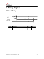
4. Timing diagram
4.1 Reset Timing
TRC
nRST
TPL
PLOCK
(Internal)
Symbol
Description
Min
Max
TRC
Reset Cycle Time
2 us
-
TPL
nRST internal PLOCK
-
150 ms
WIZ820io User Manual (WIZnet Co., Ltd.)
11
4.2 SPI Timing
TCS
nSCS
VIH
VIL
TCSS
SCLK
TCSH
VIH
TWH
VIL
TDS
MOSI
TWL
TDH
VIH
VIL
TOV
MISO
VOH
VOL
Symbol
TCHZ
TDH
HI-Z
HI-Z
Description
Min
Max
Units
80
MHz
FSCK
SCK Clock Frequency
TWH
SCK High Time
6
ns
TWL
SCK Low Time
6
ns
TCS
nSCS High Time
5
ns
TCSS
nSCS Hold Time
5
TCSH
nSCS Hold Time
5
ns
TDS
Data In Setup Time
3
ns
TDH
Data In Hold Time
3
ns
TOV
Output Valid Time
TOH
Output Hold Time
TCHZ
nSCS High to Output Hi-Z
WIZ820io User Manual (WIZnet Co., Ltd.)
-
5
0
ns
ns
ns
5
ns
12
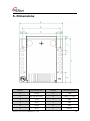
5. Dimensions
Symbol
Dimension(mm)
Symbol
Dimension(mm)
A
23.00
G
1.34
B
20.32 (2.54 x 8)
H
2.50 (+/- 0.50)
C
1.34
I
6.40
D
2.11
J
2.54
E
16.10
K
5.80
F
2.11
L
25.00
WIZ820io User Manual (WIZnet Co., Ltd.)
13
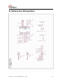
6. Reference Schematics
WIZ820io User Manual (WIZnet Co., Ltd.)
14
7. Warranty
WIZnet Co., Ltd. offers the following limited warranties applicable only to the
original purchaser. This offer is non-transferable.
WIZnet warrants our products and its parts against defects in materials and
workmanship under normal use for period of standard ONE(1) YEAR for the
WIZ820io module and labor warranty after the date of original retail purchase.
During this period, WIZnet will repair or replace a defective products or part free of
charge.
Warranty Conditions:
1. The warranty applies only to products distributed by WIZnet or our official
distributors.
2. The warranty applies only to defects in material or workmanship as
mentioned above in 3.Warranty. The warranty applies only to defects which
occur during normal use and does not extend to damage to products or
parts which results from alternation, repair, modification, faulty installation
or service by anyone other than someone authorized by WIZnet ; damage
to products
maintenance,
or
parts
caused
mishandling,
by
accident, abuse,
misapplication,
or
used
or
in
misuse,
poor
violation
of
instructions furnished by us ; damage occurring in shipment or any damage
caused by an act of God, such as lightening or line surge.
Procedure for Obtaining Warranty Service
1. Contact an authorized distributors or dealer of WIZnet for obtaining an RMA
(Return Merchandise Authorization) request form within the applicable
warranty period.
2. Send the products to the distributors or dealers together with the completed
RMA request form. All products returned for warranty must be carefully
repackaged in the original packing materials.
3. Any service issue, please contact to [email protected]
WIZ820io User Manual (WIZnet Co., Ltd.)
15
Mouser Electronics
Authorized Distributor
Click to View Pricing, Inventory, Delivery & Lifecycle Information:
WIZnet:
WIZ820io