1
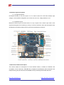
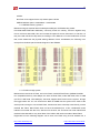
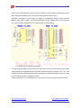
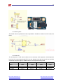
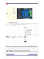
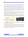
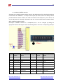
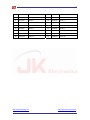
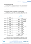
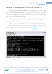
1
1. Introduction
1.1. About this Manual
This manual is intended to provide the user with an overview of the board and benefits,
complete features specifications, and set up procedures. It contains important safety information
as well.
1.2. Feedback and Update to this Manual
To help our customers make the most of our products, we are continually making additional and
updated
resources
available
on
the
JK
Electronics
technical
support
website
(http://cafe.naver.com/avrstudio).
These include manuals, application notes, programming examples, and updated software and
hardware. Check in periodically to see what’s new!
When we are prioritizing work on these updated resources, feedback from customers is the
number one influence, If you have questions, comments, or concerns about your product or
project, please no hesitate to contact us at mailto:[email protected].
1.3. Limited Warranty
JK Electronics warrants this product to be free of defects in material and workmanship for a
period of six month from date of buy. During this warranty period JK Electronics will repair or
replace the defective unit in accordance with the following process:
This limited warranty does not cover damages resulting from lighting or other power surges,
misuse, abuse, abnormal conditions of operation, or attempts to alter or modify the function of
the product.
This warranty is limited to the repair or replacement of the defective unit .In no event shall JK
Electronics be liable or responsible for any loss or damages, including but not limited to any lost
profits, incidental or consequential damages, loss of business, or anticipatory profits arising
from the use or inability to use this products.
Repairs make after the expiration of the warranty period are subject to a repair charge and the
cost of return shipping. Please contact JK Electronics to arrange for any repair service and to
obtain repair charge information.
4. License of this manual
이 매뉴얼의 JK전자에 의해서 번역, 수정, 작성 되었고 소유권 또한 JK전자의 것입니다.
소유권자의 허가를 받지 않고 무단으로 수정, 삭제하거나 배포 할 수 없습니다.
2010 Copyright by JK Electronics.
http://www.deviceshop.net
http://cafe.naver.com/avrstudio
2
1. Mini2440 Development Board Introduction .......................................................................... 3
1.1 Mini2440 Development Board Introduction................................................................. 3
1.1.1 Mini2440 development board appearance ........................................................ 5
1.1.2 Mini2440 development board hardware features ............................................. 5
1.1.3 Linux system characteristics ............................................................................. 7
1.1.4 WindowsCE 5.0 System Features ...................................................................... 8
1.1.5 WindowsCE 6.0 System Features .................................................................... 10
1.1.6 Information CD-ROM resources Help .............................................................. 11
1.2 Interface layout and jumper ........................................................................................ 14
1.2.1 Jumper Description ........................................................................................... 14
1.2.2 Interface Layout ................................................................................................. 14
1.3 Resource Interface Description.................................................................................. 14
1.3.1 address space allocation and the definition of chip select signals ............. 15
1.3.2 SDRAM memory systems ................................................................................. 16
1.3.3 FLASH storage system ..................................................................................... 16
1.3.4 Power Supply System and Interface................................................................ 17
1.3.5 Reset system...................................................................................................... 19
1.3.6 User LED............................................................................................................. 19
1.3.7 User key .............................................................................................................. 20
1.3.8 A/D input test...................................................................................................... 20
1.3.9 PWM control buzzer........................................................................................... 21
1.3.10 Serial ................................................................................................................. 21
1.3.11 USB Interface.................................................................................................... 22
1.3.12 LCD Interface.................................................................................................... 23
1.3.13 EEPROM ........................................................................................................... 24
1.3.14 Network Interface............................................................................................. 24
1.3.15 Audio Interface................................................................................................. 25
1.3.16 JTAG Interface.................................................................................................. 26
1.3.17 GPIO .................................................................................................................. 27
1.3.18 CMOS CAMERA Interface ............................................................................... 29
1.3.19 System bus interface....................................................................................... 30
http://www.deviceshop.net
http://cafe.naver.com/avrstudio
3
1. Mini2440 Development Board Introduction
1.1 Mini2440 Development Board Introduction
Mini2440 is a really cheap and practical ARM9 development board, is currently the most costeffective a learning board; It uses Samsung S3C2440 microprocessor and uses expertise stable
CPU core power supply chips and reset chip to ensure the stability of the system is running.
mini2440 the PCB with Immersion Gold process of four-layer board design, professional and
other long-wiring,
The key signal lines to ensure signal integrity, chip production using machines, mass
production; factory are subject to stringent quality control system, with this very detailed manual
that can quickly help you master the embedded Linux and WinCE development process, as
long as there are generally based on C language can be started 2 weeks.
We believe that the embedded development board can be seen not only a "light up the LED
lights or LCD" board, as long as you give it a rich soul - embedded software, all can become
more exciting, or even rebirth, we a straight in the constantly updating and enhancing the
development of embedded software, embedded system we sincerely love the cause, and this
protection holding passion and striving for perfection, we now offer Linux and Windows CE6
systems, technology and function has been achieved 2440 development board in the highest
national level, their respective bootloader and BSP are all 100% open, any person you can free
download on our website.
Users can go to our website and download the latest update to inform the latest manuals and
systems Web site: http://www.arm9.net
Mini2440 many advanced features, can be summarized as:
(1) The first paragraph is broad community support for the domestic Linux 2440 development
board (since Linux-2.6.31 start, Mini2440 was officially join the official Linux kernel)
(2) The first Linux to support the camera's 2440 Universal USB development board (similar
product is still in use in recent almost disappeared, and the shooting pretty poor Vimicro
camera, and there is no graphical interface application)
(3) First applied uniformly to support the EABI standard cross-compiler development board (still
using the same piece of the product versions of the compiler, resulting in low development
efficiency, and does not help beginners master entry)
(4) Provide the first complete BSP (based on Linux-2.6.29 (currently the Linux-2.6.32.2) and
WindowsCE 6.0) development board, and fully equipped with a graphical interface utility
applications (similar products and hardware is only part of the decoration, and is still
http://www.deviceshop.net
http://cafe.naver.com/avrstudio
4
stealing a friendly arm of the command-line test early code)
(5) The first support. NET 3.5 and Tencent QQ's 2440 development board (Oct. 2009,
WindowsCE 6.0 up Release 3)
(6) The first allows users without programming, you can simply customize Windows CE free
boot screen development board, And can start within 10 seconds top speed of the system
(similar products Windows CE boot time normally within 30 seconds even 70 seconds)
(7) The first perfect support for USB programmer update Linux (support yaffs2) and Windows
CE 5.0/6.0 development board, and supports the entire film Nand Flash back to the PC,
really suitable for mass production (no backup of similar products)
(8) First realized WinCE/Linux graphical interface using the CMOS camera can preview and
take pictures of the development board (there is no similar product in this function)
(9) The first open all the BSP source code (including Linux and Windows CE) development
board (complete BSP for beginners can learn more about the bottom, so that really only
concerns those who do develop the upper application)
(10) The first core (including WinCE and Linux) supports large pages and small pages Nand
Flash development board, so old and new users can enjoy the latest software, and use the
same way (this feature is no similar product)
(11) First in Windows CE and Linux, a simple intuitive graphical interface, you can set up
procedures to open development of automatic running board (there is no similar product in
this function)
(12) Mini2440 is currently the largest domestic retail sales in 2440 development board, by word
of mouth and friends with each other mediated, mini2440 has been praised and recognized
by many users.
http://www.deviceshop.net
http://cafe.naver.com/avrstudio
5
1.1.1 Mini2440 development board appearance
1.1.2 Mini2440 development board hardware features
(1) CPU Processor
- Samsung S3C2440A, clocked at 400MHz, the highest 533Mhz
(2) SDRAM memory
- On-board 64M SDRAM
- 32bit data bus
- SDRAM clock frequency up to 100MHz
(3) FLASH memory
- In the board 256M/1GB Nand Flash, Power-down non-volatile (user customizable
64M/128M/256M/512M/1G)
- In the board 2M Nor Flash, power-down non-volatile, has been installed BIOS.
(4) LCD display
- On-board integrated 4-wire resistive touch screen interface for direct connection of four
wire resistive touch screen.
- Support for black and white, 4-level grayscale, 16-level grayscale, 256-color, 4096 color
http://www.deviceshop.net
http://cafe.naver.com/avrstudio
6
STN LCD screen size from 3.5 inches to 12.1 inches, the screen resolution can be to
achieve 1024x768 pixels;
- Support for black and white, 4-level grayscale, 16-level grayscale, 256-color, 64K colors,
true color TFT LCD screen sizes from 3.5 inch to 12.1-inch screen resolution up to
1024x768 pixels;
- Standard configuration for the system Po 3.5 "TFT LCD, respectively, the rate 240x320,
with touch screen;
(5) Interfaces and resources
- 1 100M Ethernet RJ-45 interface (used DM9000 network chip)
- 3 serial ports
- 1 USB Host
- 1 USB Slave B-type interfaces
- 1 SD card storage interface
- 1 stereo audio output port, one microphone interface;
- 1 x 2.0mm pitch 10-pin JTAG Interface
- 4 USER Leds
- 6 USER buttons (with leads Block)
- 1 PWM control buzzer
- 1 adjustable resistance, test for AD ADC
- 1 AT24C08 chip I2C bus for I2C-bus test
- 1 x 2.0 mm pitch 20pin camera interface
- On-board real time clock battery
- Power Interface (5V), with power switch and indicator light
(6) System clock source
- 12M Passive Crystal
(7) Real-Time Clock
- Internal real time clock (with back-up lithium battery)
(8) Extension Interface
- A 34 pin 2.0mmGPIO Interface
- A 40 pin 2.0mm system bus interface
(9) Size
- 100 x 100 (mm)
(10) Operating System Support
- Linux2.6.32.2 + Qtopia-2.2.0
- Windows CE 5.0
- Windows CE 6.0 (R3)
http://www.deviceshop.net
http://cafe.naver.com/avrstudio
7
1.1.3 Linux system characteristics
(1) Version
- Linux 2.6.32.2 (BSP may be adaptive 64M/128M/256M/512M/1GB Nand Flash)
(2) Supported file system
- Yaffs2 (read-write file system recommended)
- Cramfs (compressed read-only file system, not online update data recommended)
- Ext2
- Fat32
- NFS (network file system, driver development and application ease of use)
(3) Basic driver (the driver source code are provided)
- 3 serial standard drive
- DM9000 driver
- Audio driver (UDA1341)
- RTC driver (which can save the power-down time)
- User LED lamp driver
- USB Host Driver
- True Color LCD driver (including 1024x768VGA drive)
- Touch Screen Driver
- Free universal USB drive camera driver
- USB mouse, USB keyboard driver, USB, HDD
- SD card driver that can support high-speed SD card, the maximum capacity of up to 32G
- I2C-EEPROM
- PWM control buzzer
- LCD backlight driver
- A/D converter driver
- Watchdog drivers (watchdog reset is equivalent to cold reset)
(4) Linux applications and service programs
- Busybox1.13 (Linux tool set, including the common Linux commands, etc.)
- Telnet, Ftp, inetd (Internet remote access tools and services)
- Boa (web server)
- Madplay (console-based mp3 players)
- Snapshot (screenshot console-based software)
- Ifconfig, ping, route, etc. (commonly used network tool command)
(5) Embedded graphics platform (source code provided)
http://www.deviceshop.net
http://cafe.naver.com/avrstudio
8
- Qt / Embedded 2.2
(6) Divided into two versions of x86 and arm
- Practical test procedures Qtopia
Note: The following procedures are a friendly arm of independent development, does not
provide the source code
- A / D converter test
- LED control
- Buttons button test
- I2C-EEPROM read and write test
- LCD test
- Ping Test
- Universal USB camera-free drive dynamic preview and take pictures
- Recorder
- Web browser
- Watchdog Test
- Network settings (save parameters)
- Backlight Control
- Language setting: can be set in English
- Readily write: mainly for testing the accuracy of the touch pen
- MMC/SD card and USB auto-mount and umount
1.1.4 WindowsCE 5.0 System Features
(1) Version
- Windows CE 5.0 (BSP may be adaptive 64M/128M/256M/512M/1G Nand Flash)
(2) Feature
- Support for. NET 2.0
- Support for SQL Mobile
- Support Registry Save
- Support for fast boot (10 seconds)
- Provides the most comprehensive current Windows CE 5.0 BSP (including bootloader),
And 100% open source, including
Include
- PWM control buzzer
- CMOS camera
- ADC
http://www.deviceshop.net
http://cafe.naver.com/avrstudio
9
- Watchdog
- User key (6)
- User LED (4 unit)
- Backlight control and management (to set the backlight turn off time, and through the
buttons, touch screen, keyboard, mouse wake-up)
- RTC
- DM9000 network card
- High-speed large-capacity SD cards up to 32G
- USB, USB keyboard, USB mouse, etc.
- Audio playback and recording
- Touch Screen
- LCD driver (support N35/T35, A70, L80, VGA1024x768, corresponding to resolution:
240x320, 800x480, 640x480, 1024x768)
- Defined by a simple header file can be modified to support multiple models of LCD (and
WinCE5 to maintain consistency)
- LCD rotation set
- Perfect three serial driver (defined by a simple modification can specify the header file as
DEBUG output UART0 or the common serial port, maintain and WinCE5 line)
- By modifying the Nboot header file can be easily customized progress bar's color,
position, length and width, and the boot map, film location, background
- An increase of production tools to facilitate the Logo StartLogoMaker (green software that
can run on XP or Vista,Win7)
- USB can be programmed through the normal boot screen as a bmp file new perfect
match with the above BSP, an increase of the following Windows CE utility applets,
basic
Remain the same or similar interface:
- LCD-Test: LCD test
- PWM-Buzzer: PWM control buzzer
- CMOS Camera: CMOS camera dynamic preview and take pictures
- I2C-EEPROM: I2C Bus EEPROM read and write tests based on
- Watchdog: Watchdog Test
- AD-Convert: ADC Conversion Test
- Buttons: button test
- Rotate: rotate the screen settings (save rotation results)
- Autorun-Setting: set the program to start automatically
- Recorder: recording test (the original, the interface slightly adjusted), to provide test
http://www.deviceshop.net
http://cafe.naver.com/avrstudio
10
source code
- Serial Assistant: Provides test source code
- LED test: test source code available
1.1.5 WindowsCE 6.0 System Features
(1) Version
- Windows CE Embedded 6.0 (BSP may be adaptive 64M/128M/256M/512M/1G Nand
Flash)
(2) Feature
- Based on the latest patch Release3 (2009.10 release, the user can add Mobile QQ
components, relatively large)
- Support for. NET 3.5
- Support for a comprehensive directory to read and write, you can install additional thirdparty software, such as PenPower handwriting input method.
- Support for fast boot (10 seconds)
- Provides the most comprehensive current WindowsCE 6.0 BSP (including bootloader), and
100% open source, including
Include:
- PWM control buzzer
- CMOS camera
- I2C-EEPROM read and write
- ADC ADC
- Watchdog
- User key (6)
- User LED (4 unit)
- Backlight control and management (to set the backlight turn off time, and through the
buttons, touch screen, keyboard, mouse wake-up)
- RTC
- DM9000 network card
- High-speed large-capacity SD cards up to 32G
- USB, USB keyboard, USB mouse, etc.
- Audio playback and recording
- Touch Screen
- LCD driver (support N35/T35, A70, L80, VGA1024x768, corresponding to resolution:
240x320, 800x480, 640x480, 1024x768)
- Defined by a simple header file can be modified to support multiple models of LCD (and
WinCE5 to maintain consistency)
http://www.deviceshop.net
http://cafe.naver.com/avrstudio
11
- LCD rotation set
- Perfect three serial driver (defined by a simple modification can specify the header file as
DEBUG output UART0 or the common serial port, maintain and WinCE5 line)
- By modifying the Nboot header file can be easily customized progress bar's color, position,
length and width, and the boot map, film location, background
- An increase of production tools to facilitate the Logo StartLogoMaker (green software that
can run on XP or Vista,Win7)
- USB can be programmed through the normal boot screen as a bmp file
new perfect match with the above BSP, an increase of the following Windows CE utility
applets, basic and Qtopia Apps
Remain the same or similar interface:
- LCD-Test: LCD test
- PWM-Buzzer: PWM control buzzer
- CMOS Camera: CMOS camera dynamic preview and take pictures
- I2C-EEPROM: I2C Bus EEPROM read and write tests based on
- Watchdog: Watchdog Test
- AD-Convert: ADC Conversion Test
- Buttons: button test
- Rotate: rotate the screen settings (save rotation results)
- Autorun-Setting: set the program to start automatically
- Recorder: recording test (the original, the interface slightly adjusted), to provide test source
code
- Serial Assistant: Provides test source code
- LED test: test source code available
1.1.6 Information CD-ROM resources Help
The development board provides a DVD data disc, mainly the following:
(1) Linux development related to the various source code and tools
Include:
- A unified cross-compiler arm-linux-gcc-4.3.2 with EABI
- The latest Linux kernel source code package Linux-2.6.32.2, contains a very full sound
BSP
- Embedded GUI Qte / Qtopia source code package: x86-qtopia and arm-qtopia, PC version
and the corresponding ARM version, containing compiled script.
- Busybox source code package and the default configuration file
http://www.deviceshop.net
http://cafe.naver.com/avrstudio
12
- Bootloader source code (vboot): using arm-linux-gcc cross-compiler
- Linux Programming Example: with the serial port, PWM, AD, EEPROM, multi-threading,
etc.
(2) Windows CE5/6 related to the development of various source code and software
Include:
- WindowsCE 5.0/6.0 of the BSP, is the 2440 development board in the most perfect BSP,
100% open source
- Bootloader source code (nboot): use of ADS can be compiled, Windows CE 5.0/6.0 share
the same bootloader, can achieve quick start, fast display boot Logo, support 2M within
the 24-bit true color bmp photo (16-bit to 1024x768 the bmp picture size 1.5M)
- Produced on WindowsCE 5.0/6.0 SDK, which is two different versions of the SDK
- Mini2440.pbxml: core sample project, bringing together the most commonly used
components, users can be increased on this basis delete the kernel works for their needs
- StartLogoMaker: the arm-friendly and easy to use self-developed production starts Logo
(3) uCos2 source code
uCos2 is provided by a User transplantation, its functionality and performance are very limited,
in this study and reference use only user
(4) 2440test source code
This is the original of 2440test Samsung improved on a bare metal test program, compiled using
the ADS, only users in this study learning reference.
Test items include: interrupt key test, RTC Real Time Clock test, ADC DAC testing, IIS audio
playback wav test, IIS audio recording test, touch screen test, I2C bus to read and write
AT24C08 test, Samsung 3.5 "LCD, 640x480 True color LCD test, LCD2VGA output test
(5) Windows platform software utility
To facilitate the use of domestic users easier development board kit, we have produced and
collected some commonly used Windows platform software tool, and be unified on the CD
"windows platform tools" directory, including:
- H-JTAG: To support the programming of various NOR Flash
- Dnw: used to implement USB Download
- ActiveSync: Microsoft, PC Sync Software
- Usb Download Driver: development board BIOS mode required for PC-side driver
(6) Various data sheets and schematic
Includes the development board schematic (pdf format and is divided into protel99se format)
http://www.deviceshop.net
http://cafe.naver.com/avrstudio
13
and the package database, development board each chip data hand books, development board
supporting the LCD data sheet, and the LCD driver board schematics, etc.
(7) Other References
In order to facilitate user learning to use the development board, we also from time to time and
learning in the online collection of some of the information related to the development board,
also some are provided by the users and impartial.
(8) User Manual
Development board user manual, users can download the latest version of our site the user
manual.
http://www.deviceshop.net
http://cafe.naver.com/avrstudio
14
1.2 Interface layout and jumper
1.2.1 Jumper Description
Development board is only one jumper J2, it is used to select the LCD driver board's input
voltage, in the standard configuration, the access 3.5-inch LCD, voltage selection is 5V.
1.2.2 Interface Layout
Mini2440 interface layout as shown below, it is very compact 100 x 100mm open area on the
exquisite arrangements for made by a variety of common interfaces used, and also leads for the
development and testing needs of the IO ports and redundant bus interface:
1.3 Resource Interface Description
This section details the development of each interface board or module pin definition and
occupation of CPU resources, CD-ROM also complete the development board schematic and
footprint library (into pdf format and Protel99SE format) for development board reference.
http://www.deviceshop.net
http://cafe.naver.com/avrstudio
15
1.3.1 address space allocation and the definition of chip select signals
S3C2440 supports two boot modes: one is start from the Nand Flash (MINI2440 that is such); a
Nor Flash from the start. In two starts this mode, each chip select for memory space allocation is
different, as shown below:
Above,
The left is nGCS0 the Nor Flash chip select start mode, the storage allocation map;
The right is the Nand Flash memory boot mode distribution map;
Description: SFR Area Control for the special register address
Here is the device address space allocation and definition of its chip select before carrying out
the device address shows, there is one thing to note, nGCS0 chip select space in a different
startup mode.
The mapping device is not the same. From the above chart to know:
(1) NAND Flash boot mode, the internal 4K Bytes BootSram is mapped to nGCS0 films selected
Space;
(2) Nor Flash boot mode (non-Nand Flash boot mode), and connected to the external memory
http://www.deviceshop.net
http://cafe.naver.com/avrstudio
16
nGCS0.
Nor Flash to be mapped to the chip select space nGCS0
SDRAM address space: 0x30000000 ~ 0x34000000
1.3.2 SDRAM memory systems
Mini2440 using two external total of 64M bytes 32M bytes of SDRAM chip (model:
HY57V561620FTP/MT48LC16M16A2), commonly known as memory, and then together they
form a 32-bit bus data width, this can increase the speed of access; because it is, and then, so
they are used nGCS6 as chip select, according to CPU Manual 5-2 in the introduction to know
that, which determines the physical starting address of their 0x30000000, the following is an
excerpt from mini2440 part schematic diagram of the SDRAM.
1.3.3 FLASH storage system
Mini2440 have two kinds of Flash, one is Nor Flash, model SST39VF1601 (AMD29LV160DB
Pin compatible with this), size 2Mbyte; the other is Nand Flash, model K9F1G08, size of 128M
(old This is K9F1208, size 64Mbyte). S3C2440 supports both Flash boot the system, through
the toggle switch S2. You can choose from NOR or NAND boot the system from. Most of the
actual product enough to use a Nand Flash, because we learn to develop user-friendly, so also
retained Nor Flash. Nand Flash does not have the address line, it has a dedicated control
interface connected with the CPU, data bus for the 8-bit, but This does not mean Nand Flash
read and write data will be very slow. Most of the USB or SD cards are made of Nand Flash
Equipment from the following diagram can be seen, Nor Flash using A1-A22 address bus, a
http://www.deviceshop.net
http://cafe.naver.com/avrstudio
17
total of 22 and 16 data bus and CPU connection, please note that address is started from the A1,
which means that read and write it every time the smallest unit is the 2-byte,
Therefore, according to the schematic, the design is compatible to support a total maximum
8Mbyte of Nor Flash, actually our development board only the address lines A1-A20, because
A21, A22 connected SST39V1601 the corresponding pin is left floating.
1.3.4 Power Supply System and Interface
The development board's power system is simple, direct use of an external 5V power supply
chips produced by the Department Buck System needs three kinds of voltage: 3.3V, 1.8V, 1.25V.
Please note that this development board is not designed for handheld mobile devices, so it does
not have the best power management circuits.
Power off the system is controlled by the S1 DIP switches, it can not switch machine software.
http://www.deviceshop.net
http://cafe.naver.com/avrstudio
18
To facilitate the user external power supply, we also designed a power interface CON8, it is a
white 2.0mm pitch, single row socket in the middle are the "ground", both sides are 5V. Note
that both 5V is not connected, One of the external power supply connected to 5V, the other is
connected through the slide switch S1 after the 5V.
Their relationship and the corresponding physical link shown below nominal:
http://www.deviceshop.net
http://cafe.naver.com/avrstudio
19
1.3.5 Reset system
This board uses the professional reset chip MAX811 needed to achieve low CPU reset, see
below:
1.3.6 User LED
The development of LED status indicators most commonly used equipment, the development
board has four user-programmable LED, they are straight connected with the CPU of the GPIO
connected, active-low (light), a detailed resource consumption following table:
LED1
LED2
LED3
LED4
GPB5
GPB6
GPB7
GPB8
Alternate
nXBACK
nXREQ
nXDACK1
nDREQ1
Pin Name
nLED_1
nLED_2
nLED_3
nLED_4
GPIO
http://www.deviceshop.net
http://cafe.naver.com/avrstudio
20
1.3.7 User key
The development board a total of 6 users test button, they are the direct extraction from the
CPU interrupt pin, a low-power level trigger, these pins can be multiplexed and special features
for the GPIO port, leads them to customers for other purposes,
This 6-pin also leads through CON12, and CON12 6 button defined as follows:
K1
K2
K4
K4
K5
K6
Interrupt
EINT8
EINT11
EINT13
EINT14
EINT15
EINT19
Reuse GPIO
GPG0
GPG3
GPG5
GPG6
GPG7
GPG11
No
nSS1
SPIMISO1
SPIMOSI1
SPICLK1
TCLK1
CON12.1
CON12.2
CON12.3
CON12.4
CON12.5
CON12.6
Special
Function
CON12 Pin
Description: CON12.7 for the power supply (3.3V), CON12.8 the ground (GND)
1.3.8 A/D input test
The development board can lead to a total of 4-way A / D (analog-digital conversion) conversion
channels, which in the board CON4-GPIO Interface (see GPIO Interface Description), to
facilitate testing, AIN0 connected to the development board of the adjustable resistor W1,
principle figure shown below.
http://www.deviceshop.net
http://cafe.naver.com/avrstudio
21
1.3.9 PWM control buzzer
Development board buzzer SPEAKER by PWM control, the schematic diagram shown below,
which can pass GPB0 through the software set to PWM output.
1.3.10 Serial
S3C2440 own a total of three serial ports UART0, 1,2, which UART0, 1 can be combined into a
fully functional serial port, in most applications, we only use three simple serial port functions
(the development board to provide the Linux and WinCE this drive is also set), known as the
send (TXD) and receive (RXD), which correspond to the board of CON1,
CON2, CON3, these three interfaces are the direct leads from the CPU, and is TTL level. To
http://www.deviceshop.net
http://cafe.naver.com/avrstudio
22
facilitate users, their made in the UART0 RS232 level translation, which corresponds to COM0,
can be directly attached to each other through connection and PC, Information.
CON1, CON2, CON3 in the development of board and schematic location of the connection
defined in the corresponding figure below.
1.3.11 USB Interface
The development board has two USB interfaces, one USB Host, it and the ordinary PC's USB
interface is the same, Can connect USB camera, USB keyboard, USB mouse, USB, etc.
common USB peripherals, the other is USB Slave, We generally use it to download to the target
board, when the development board loaded with WinCE system, it can ActiveSync
Synchronization software, and Windows systems, when the development board loaded Linux
systems, there is not the appropriate driver and application.
To facilitate the users to program control USB Slave and PC-off, we set USB_EN signal, as
shown, it use of CPU resources GPC5.
We will provide more extensive peripheral USB Host application, please always pay attention to
our website updates.
http://www.deviceshop.net
http://cafe.naver.com/avrstudio
23
1.3.12 LCD Interface
The development board's LCD interface is a 41Pin 0.5mm pitch, white seat, which contains
commonly used in LCD most of the control signals (line scan field, the clock and enable, etc.),
and complete RGB data signals (RGB 8:8:8 output, The maximum support 16 million colors
LCD); for users to easily test, also raises PWM output (GPB1 can send registers is configured to
PWM), and reset signal (nRESET), which is a backlight control signal LCD_PWR.
In addition, 37,38,39,40 for the four-wire touch screen interface, they can connect directly using
the touch screen. Figure of J2 for the LCD driver board power supply select signal, we now use
the drive board 5V supply.
http://www.deviceshop.net
http://cafe.naver.com/avrstudio
24
1.3.13 EEPROM
The development board has a direct connection to CPU signal pins of I2C EEPROM chip
AT24C08, It a capacity of 256 byte, in this mainly for I2C bus for user testing and use, it does
not store specific parameters.
1.3.14 Network Interface
The board uses the DM9000 card chip, it can be adaptive 10/100M network, RJ45 connector
internal already contains a coupling coil, so no other access network transformer, you can use
an ordinary cable to connect the development board to your routers or switches.
http://www.deviceshop.net
http://cafe.naver.com/avrstudio
25
Note: Each development board's network MAC address is the same, it can be set by software,
for Linux users, relevant sections of the manual introduces 2.4; for WinCE users, you can refer
to the BSP which the DM9000 driver code and registry files (platform.reg).
1.3.15 Audio Interface
S3C2440 built-in I2S bus interface, direct external 8 / 16 bit stereo CODEC, the development
board used I2S bus-based audio decoding system UDA1341 chip, the chip initializes internal
registers and settings are taken bus connection with the L3-bus control to achieve, where we
followed the design of Samsung's public board were using the CPU's GPB2, GPB3, GPB4 port
analog realization of L3-Bus specification L3MODE, L3DATA, L3CLOCK, they are initialized
after completion UDA1341 no longer useful, so the three control lines can also be used to
achieve common SCM simulation.
The output audio system used for the development of 3.5mm diameter jack board, enter in two,
all the way for the wheat board grams of the wind, another road leads through the CON10 white
2.0mm socket. Two audio input channels drive is a bit different, MIC corresponds to the current
on-board recording channel is used, pay attention: The development board is not a professional
recording equipment, audio output into the processing circuit Hen simple recording source close
http://www.deviceshop.net
http://cafe.naver.com/avrstudio
26
to the microphone as far as possible.
1.3.16 JTAG Interface
When the development board from the patch works offline, which is no process, then we
generally through the JTAG interface to the programming.
The first program is Supervivi, you can use the USB port with Supervivi download a more
complex system procedures, This in later chapters you can see.
In addition, JTAG interface, the development of the most common use is the single-step
debugging, either on the market common H-JTAG, and other simulation debugger, JTAG
interface, eventually connect through. Standard JTAG Interface
Is a 4-wire: TMS, TCK, TDI, TDO, respectively, mode selection, clock, data input and data
output lines, coupled with power and ground, generally a total of six lines is enough; for the
convenience of debugging, most of the simulator also provides a reset signal.
Therefore, the standard JTAG interface, is whether the JTAG signal lines mentioned above, is
not 20Pin or 10Pin formal definition of these and other performance. This is like a USB interface,
can be a side can also be flat, can also be other forms, as long as these interfaces include a
complete JTAG signal lines can be called a standard JTAG interfaces.
The development board provides a JTAG standard signal contains the complete 10 Pin JTAG
interface, the definition of the pin shown in Figure.
http://www.deviceshop.net
http://cafe.naver.com/avrstudio
27
Description: Linux or WinCE for the plan is committed to the development of beginner, JTAG
interface, there is no fundamental meaning and purpose, because most development board had
already provided the perfect BSP, which includes the most common serial and network
contact, and USB communication port, when the system loaded with Linux or WinCE can run
the system, users can fully. These advanced operating system itself has various debugging
functions, then do not need JTAG interface; even if you can to be tracked, but in view of the
operating system itself complex, interface range, single-step debug like needle in a haystack,
meaningless. Think you do use the PC machine will know, perhaps you have never seen or
even heard of who in the PC motherboard.
Insert an emulator to debug PCI interface Windows XP or Linux this driver. This is why you
through common to speak or hear so many people drive in the "transplant", because most
people refer to the realization of the older generation do drive.
JTAG only for those who do not intend to use the operating system, or the use of simple
operating system (such as uCos2, etc.) users helpful. Provided most of the development board
or BIOS Bootloader is already a basic system intact, and therefore do not need to step through.
1.3.17 GPIO
GPIO is general purpose input output short, the development board with a 34 Pin 2.0mm pitch
GPIO interface nominal for the CON4, Figure.
In fact, CON4 not only contains a lot of surplus of GPIO pins, also contains a number of other
CPU pins, If AD0-AIN3, CLKOUT so. What you see in the figure SPI interfaces, I2C interfaces,
GPB0 and GPB1 so, It they actually GPIO, but in special function interface to the nominal
definition, these are available through the corresponding CPU storage to set the change of their
use, details of the interface resource table below.
http://www.deviceshop.net
http://cafe.naver.com/avrstudio
28
CON4
1
Pin Name
VDD5V
Description
5V power supply
CON4
2
Pin Name
VDD33V
(input or output)
Description
3.3V power supply
(output)
3
GND
GND
4
nRESET
Reset signal (output)
5
AIN0
AD input channel 0
6
AIN1
AD input channel 1
7
AIN2
AD input channel 2
8
AIN3
AD input channel 3
9
EINT0
EINT0/GPF0
10
EINT11
EINT1/GPF1
11
EINT2
EINT2/GPF2
12
EINT13
EINT3/GPF3
13
EINT4
EINT4/GPF4
14
EINT15
EINT5/GPF5
15
EINT6
EINT6/GPF6
16
EINT18
EINT8/GPG0
17
EINT9
EINT9/GPG1
18
EINT11
EINT11/GPG3/nSS1
19
EINT13
EINT13/GPG5/SPIMISO1
20
EINT14
EINT14/GPG6/SPIMOSI1
21
EINT15
EINT15/GPG7/SPICLK1
22
EINT17
EINT17/GPG9/nRST1
23
EINT18
EINT18/GPG10/nCTS1
24
EINT19
EINT19/GPG11
25
SPIMISO
SPIMISO /GPE11
26
SPIMOSI
SPIMOSI /EINT14/GPG6
27
SPICLK
SPICLK /GPE13
28
nSS_SPI
nSS_SPI /EINT10/GPG2
29
I2CSCL
I2CSCL/GPE14
30
I2CSDA
I2CSDA/GPE15
31
GPB0
TOUT0/ GPB0
32
GPB1
TOUT1/ GPB1
33
CLKOUT0
CLKOUT0/GPH9
34
CLKOUT1
CLKOUT1/GPH10
http://www.deviceshop.net
http://cafe.naver.com/avrstudio
29
1.3.18 CMOS CAMERA Interface
S3C2440 with a CMOS camera interface board in the development of the interface through the
nominal leads to CAMERA. It Is a 20-pin 2.0mm pitch pin holder, users can directly use the
provided CAM130 camera module; fact CAM130 camera module without any circuit above, it is
only a relay board, it is directly connected to the use of the model ZT130G2 camera module,
which is defined as shown below.
Description: CAMERA interface is a multiplexed port, it can be changed by setting the
appropriate GPIO enable register used, the following table is a list of its corresponding GPIO pin.
CON4
Pin Name
Description
CON4
Pin Name
Description
1
I2CSDA
GPE15
2
I2CSCL
GPE14
3
EINT20
GPG12
4
CAMRST
GPJ12
5
CAMCLK
GPJ11
6
CAM_HREF
GPJ10
7
CAM_VSYNC
GPJ9
8
CAM_PCLK
GPJ8
9
CAMDATA7
GPJ7
10
CAMDATA6
GPJ6
11
CAMDATA5
GPJ5
12
CAMDATA4
GPJ4
13
CAMDATA3
GPJ3
14
CAMDATA2
GPJ2
15
CAMDATA1
GPJ1
16
CAMDATA0
GPJ0
17
VDD33V
3.3V Power
18
VDD_CAM
VDD_CAM
19
VDD18V
1.8V Power
20
GND
GND
http://www.deviceshop.net
http://cafe.naver.com/avrstudio
30
1.3.19 System bus interface
The development board system bus interface CON5, it contains a total of 16 data lines (D0D15), 8 address lines (A0-A6, A24), and some control signal lines (chip select, read and write,
reset, etc.), CON5 can provide 5V voltage input field out; in fact, very few users peripheral bus
extension. The following is a detailed CON5 pin definition description.
CON5
Pin Name
Description
1
VDD5V
5V Power(In/Out)
3
EINT17
5
7
CON5
Pin Name
Description
2
GND
GND
Interrupt 17(In)
4
EINT18
Interrupt 18(In)
EINT3
Interrupt 3(In)
6
EINT9
Interrupt 9(In)
nGCS1
Chip Select 1
8
nGCS2
Chip Select 2
Phy Address:0x08000000
9
nGCS3
Chip Select 3
Phy Address:0x10000000
10
nGCS5
Chip Select 5
Phy Address:0x18000000
11
LnOE
13
nWAIT
15
nXDACK0
17
Read Enable
Phy Address:0x28000000
12
LnWE
14
nRESET
nXDACK0
16
nXDREQ0
nXDREQ0
LADDR0
ADDR 0
18
LADDR1
ADDR 1
19
LADDR2
ADDR 2
20
LADDR3
ADDR 3
21
LADDR4
ADDR 4
22
LADDR5
ADDR 5
http://www.deviceshop.net
Write Enable
http://cafe.naver.com/avrstudio
31
23
LADDR6
ADDR 6
24
LADDR24
ADDR 24
25
LDATA0
DATA 0
26
LDATA1
DATA 1
27
LDATA2
DATA 2
28
LDATA3
DATA 3
29
LDATA4
DATA 4
30
LDATA5
DATA 5
31
LDATA6
DATA 6
32
LDATA7
DATA 7
33
LDATA8
DATA 8
34
LDATA9
DATA 8
35
LDATA10
DATA 10
36
LDATA11
DATA 11
37
LDATA12
DATA 12
38
LDATA13
DATA 13
39
LDATA14
DATA 14
40
LDATA15
DATA 15
http://www.deviceshop.net
http://cafe.naver.com/avrstudio